WO2012111639A1 - モジュール間通信装置 - Google Patents
モジュール間通信装置 Download PDFInfo
- Publication number
- WO2012111639A1 WO2012111639A1 PCT/JP2012/053318 JP2012053318W WO2012111639A1 WO 2012111639 A1 WO2012111639 A1 WO 2012111639A1 JP 2012053318 W JP2012053318 W JP 2012053318W WO 2012111639 A1 WO2012111639 A1 WO 2012111639A1
- Authority
- WO
- WIPO (PCT)
- Prior art keywords
- signal line
- line
- inter
- lead
- module
- Prior art date
- Legal status (The legal status is an assumption and is not a legal conclusion. Google has not performed a legal analysis and makes no representation as to the accuracy of the status listed.)
- Ceased
Links
Images














Classifications
-
- H—ELECTRICITY
- H04—ELECTRIC COMMUNICATION TECHNIQUE
- H04B—TRANSMISSION
- H04B5/00—Near-field transmission systems, e.g. inductive or capacitive transmission systems
- H04B5/40—Near-field transmission systems, e.g. inductive or capacitive transmission systems characterised by components specially adapted for near-field transmission
- H04B5/48—Transceivers
-
- H—ELECTRICITY
- H04—ELECTRIC COMMUNICATION TECHNIQUE
- H04B—TRANSMISSION
- H04B5/00—Near-field transmission systems, e.g. inductive or capacitive transmission systems
- H04B5/20—Near-field transmission systems, e.g. inductive or capacitive transmission systems characterised by the transmission technique; characterised by the transmission medium
- H04B5/28—Near-field transmission systems, e.g. inductive or capacitive transmission systems characterised by the transmission technique; characterised by the transmission medium using the near field of leaky cables, e.g. of leaky coaxial cables
-
- H—ELECTRICITY
- H04—ELECTRIC COMMUNICATION TECHNIQUE
- H04B—TRANSMISSION
- H04B5/00—Near-field transmission systems, e.g. inductive or capacitive transmission systems
- H04B5/20—Near-field transmission systems, e.g. inductive or capacitive transmission systems characterised by the transmission technique; characterised by the transmission medium
- H04B5/22—Capacitive coupling
-
- H—ELECTRICITY
- H04—ELECTRIC COMMUNICATION TECHNIQUE
- H04B—TRANSMISSION
- H04B5/00—Near-field transmission systems, e.g. inductive or capacitive transmission systems
- H04B5/20—Near-field transmission systems, e.g. inductive or capacitive transmission systems characterised by the transmission technique; characterised by the transmission medium
- H04B5/24—Inductive coupling
-
- H—ELECTRICITY
- H04—ELECTRIC COMMUNICATION TECHNIQUE
- H04B—TRANSMISSION
- H04B2203/00—Indexing scheme relating to line transmission systems
- H04B2203/54—Aspects of powerline communications not already covered by H04B3/54 and its subgroups
- H04B2203/5462—Systems for power line communications
- H04B2203/5483—Systems for power line communications using coupling circuits
-
- H—ELECTRICITY
- H10—SEMICONDUCTOR DEVICES; ELECTRIC SOLID-STATE DEVICES NOT OTHERWISE PROVIDED FOR
- H10W—GENERIC PACKAGES, INTERCONNECTIONS, CONNECTORS OR OTHER CONSTRUCTIONAL DETAILS OF DEVICES COVERED BY CLASS H10
- H10W72/00—Interconnections or connectors in packages
- H10W72/90—Bond pads, in general
- H10W72/931—Shapes of bond pads
- H10W72/932—Plan-view shape, i.e. in top view
Definitions
- the present invention relates to an inter-module communication device, and, for example, to a configuration for performing high-speed wireless data communication between close modules.
- an inter-module communication device which can perform high-speed wireless data communication when a plurality of modules such as performing data communication without contact between a memory card and a PC are in proximity.
- an inter-module communication device it is also expected to wirelessly communicate between semiconductor integrated circuit chips over packages in a PoP (package on package) in which a plurality of packages in which semiconductor integrated circuit chips are sealed are stacked. .
- PoP package on package
- the present inventor uses the inductive coupling of coils formed by printed circuit boards (Printed Circuit Boards; PCBs) and interconnections of semiconductor integrated circuit chips, that is, magnetic field coupling, to perform data communication between mounting boards and between semiconductor integrated circuit chips.
- PCBs printed Circuit Boards
- PCBs printed Circuit Boards
- semiconductor integrated circuit chips that is, magnetic field coupling
- Non-Patent Document 1 a coil formed by wiring of a semiconductor integrated circuit chip sealed in a package and an inductive coupling by a coil of a flexible printed circuit (FPC) mounted on the surface of the package are used.
- the data in the semiconductor integrated circuit chip sealed in the package can be detected from the outside of the package and used for evaluation or debugging of a system configured with the semiconductor integrated circuit chip or the semiconductor integrated circuit chip.
- inductive coupling is performed by a coil pair in which a processor semiconductor integrated circuit chip and a memory semiconductor integrated circuit chip stacked and mounted in one package are formed by the interconnections of the respective semiconductor integrated circuit chips. It can be used to communicate at high speed between the two. If this technology is applied, the processor reads and writes data in the memory by wireless data communication using inductive coupling of coils formed in the package in a state where the package mounting the processor and the package mounting the memory are stacked and mounted. can do.
- the memory card and the PC can perform data communication in a noncontact manner by using inductive coupling by a coil pair on a printed circuit board.
- Patent Document 1 it is possible to wirelessly communicate between two modules by arranging differential transmission lines consisting of two transmission lines arranged in parallel in parallel in the same direction.
- a bidirectional transmission system can be constructed by electromagnetically or capacitively coupling a movable driver stage with two symmetrically arranged conductors via a coupling element.
- differential signals are input to two microstrip lines using two microstrip lines disposed via a dielectric film on a ground plane as directional couplers. Wireless communication can be made between the two modules.
- JP 2008-278290 A Japanese Patent Publication No. 2003-533130 JP, 2007-049422, A Japanese Patent Application Publication No. 07-141079 JP 2001-027918 A JP 2002-123345 A JP 2004-318451 A
- a coil used for wireless data communication between modules or between semiconductor integrated circuit chips has a capacitance C parasitic in addition to the inductance L as in a normal coil, so a certain frequency, ie, LC resonance occurs at the self resonance frequency.
- a certain frequency ie, LC resonance occurs at the self resonance frequency.
- the upper limit of the communication speed that can be achieved by inductive coupling of the coil is about 1/3 to 1/2 of the self-resonant frequency of the coil.
- the self resonant frequency of the coil is inversely proportional to the square root of the LC product of the coil. As the communication distance increases, a larger coil is required, so C increases and the self-resonance frequency decreases.
- the diameter of the coil is about 100 ⁇ m, which is twice that diameter.
- the bandwidth of the channel is 10 GHz or more, and the communication speed is determined by the circuit of the transceiver.
- communication distance between modules becomes long.
- the communication distance is 1 mm
- a coil with a diameter of about 1 mm is required, and the self-resonant frequency of the coil on the PCB is about 3 GHz, so the communication speed is determined by the communication channel, 1 Gb / s (1 G / s)
- the upper limit is about a bit).
- T x and R x are respectively a transmitting circuit and a receiving circuit.
- the impedance of the transmission line (referred to as a characteristic impedance) does not change significantly in the signal band, but the impedance of the coil changes in proportion to the frequency. Therefore, it is difficult to match the impedance at the connection point between the two, and the signal is reflected to deteriorate the signal quality, and reliable communication can not be performed.
- the distance is longer than about 0.4 mm, it must be treated as a transmission line, and impedance matching is required. That is, in the prior art which used the inductive coupling of the coil for the communication path, it was necessary to install the integrated circuit provided with the transceiver within 0.4 mm from the coil. However, coils of 1 mm in diameter can be connected within 0.4 mm apart from each other so as not to cross-talk, at most 4 coils, making it difficult to connect with more coils. Furthermore, due to equipment design constraints, it is often desirable to locate integrated circuit devices remotely.
- the inventor of the present invention found that, when two modules are in close proximity, the impedance of the transmission line is affected by the other transmission line due to the proximity effect and becomes a value different from the characteristic impedance Z 0 of the single transmission line. It came to the conclusion that such changes in impedance can not be ignored.
- the impedance of the transmission line in such a coupled state is referred to as a coupled system impedance and expressed as Z 0 -coupled .
- the present invention aims at making the communication channel faster (in a wider band) than inductive coupling by matching as coupling system impedance and thereby reducing reflections.
- the present invention provides a first signal line having a characteristic impedance of Z 01 in a module-to-module communication device, and a feedback path of the first signal line.
- a first module having at least a first termination member terminating a feedback signal line, the first signal line, and the first feedback signal line, and a first semiconductor integrated circuit device provided with a transmission / reception circuit;
- a second signal line having an impedance of 02, a second feedback signal line for providing a feedback path of the second signal line, a second termination member for terminating the second signal line and the second feedback signal line,
- a second module having at least a second semiconductor integrated circuit device having a transmitting / receiving circuit is disposed close to each other, facing each other, and the first termination member and the first terminal member Impedance of the termination member, characterized in that a coupling system impedance reflecting the proximity effect in the state of bonding between different ones of the first module and the second module and the Z 01 and Z 02.
- the termination members having coupling system impedance reflecting the proximity effect in the coupling state of the first module and the second module are used in each module, signal reflection can be effectively eliminated. Further, since communication is performed in baseband without modulation using a carrier signal, high-speed communication can be performed with a simpler configuration.
- the first signal line is a signal line provided on a first insulating substrate and having a length of 1/10 or more of a signal wavelength
- a first semiconductor integrated circuit device is connected to the first signal line and the first feedback signal line
- the second signal line has a length of 1/10 or more of the signal wavelength provided on the second insulating substrate.
- the second semiconductor integrated circuit device is connected to the second signal line and the second feedback signal line, and the first signal line and the second signal line are at least one of them.
- the first feedback signal line and the second feedback signal line at least partially projectively overlap each other when viewed from the stacking direction, and the first signal line and the second feedback signal line overlap with each other.
- the present invention is characterized in that, in (2), the feedback signal combination is the same as or stronger than the signal combination.
- the feedback signal coupling is the same as or stronger than the signal coupling.
- the first feedback signal line forms a coplanar structure with the first signal line
- the second feedback signal line corresponds to the second signal line.
- noise immunity can be enhanced by making the feedback signal line coplanar with the signal line.
- the first feedback signal line has a symmetrical structure with respect to both sides of the first signal line
- the second feedback signal line is the second signal line. It is characterized in that it has a symmetrical structure on both sides of.
- a first electromagnetic shield layer is provided on the surface opposite to the surface on which the first signal line of the first insulating substrate is disposed, and the second insulation
- a second electromagnetic shield layer is provided on the side opposite to the side on which the second signal line of the flexible substrate is disposed.
- either the distance between the first signal line and the second signal line or the overlapping width between the first signal line and the second signal line is It is characterized in that the coupling state of the first signal line and the second signal line is different in the propagation direction of the signal by being different in the propagation direction of the signal.
- the frequency characteristic of the coupling coefficient of the signal line is made flat, and a wide band coupler is realized. Can.
- one of the first module and the second module sandwich a dummy coupler with respect to the first signal line or the second signal line.
- a third termination member having a signal line and a third feedback signal line for providing a feedback path of the third signal line, the third termination member terminating the third signal line and the third feedback signal line, and the third signal
- a third semiconductor integrated circuit device including a transmission / reception circuit connected to a line and the third feedback signal line.
- the first signal line has a coupling system impedance that reflects a proximity effect in a coupling state of the first module and the second module.
- the second signal line is connected to the first semiconductor integrated circuit device through a transmission line, and the second signal line is connected to the second semiconductor integrated circuit device through a second lead-out transmission line having the coupling system impedance. It is characterized by
- the semiconductor integrated circuit device can be disposed at a position away from the signal line, and the degree of freedom in design is increased.
- At least a portion opposite to the surface on which the first signal line of the first insulating substrate is disposed is a portion facing the first signal line A first plane, and at least a portion of the second insulating substrate opposite to the surface on which the second signal line is disposed is a portion facing the second signal line; It is characterized by having two planes.
- the electric lines of force between the interconnects of the coupler can be obtained by making at least a portion facing the first signal line and the second signal line a dropout. Can be concentrated and the coupling degree of the coupler can be raised.
- the line width of the first signal line is larger than or equal to the line width of the first leading transmission line
- the line width of the second signal line is The line width of the second lead-out transmission line is equal to or larger than the line width of the second lead-out transmission line.
- the first extraction transmission line and the second extraction line are used. It is characterized in that the transmission lines extend in different directions. In this way, if the coupling between the lead-out transmission lines is weakened by pulling out the lead-out transmission lines in different directions, the coupled system impedance of the lead-out transmission lines becomes equal to the characteristic impedance, so the variation of the distance between modules The impedance can be designed without being affected by
- the facing distance between the first lead-out transmission line and the second lead-out transmission line is the distance between the first signal line and the second signal line. It is characterized in that it is wider than the interval. By employing such a configuration, it is possible to weaken the coupling between the leading transmission lines.
- a first auxiliary electromagnetic shield layer for shielding the first lead-out transmission line may be provided.
- the side surface of the coupling portion between the first signal line and the first leading transmission line is a curved surface
- the second signal line and the second leading It is characterized in that the side surface of the connection portion with the transmission line is a curved surface.
- a transmission line for adjusting the first impedance is provided at an end of the first signal line opposite to the coupling portion with the first extraction transmission line.
- a first impedance matching circuit is connected to the first impedance adjusting transmission line, and a second impedance adjusting transmission line is connected to an end of the second signal line opposite to a coupling portion with the second lead transmission line.
- the second impedance matching circuit is connected to the second impedance adjustment transmission line.
- the transmission line for impedance adjustment and the impedance matching circuit it is possible to accurately obtain the impedance matching even if there is a manufacturing variation in the impedance of the coupled line or a variation in the distance between the lines. This prevents signal reflection and enables high-speed communication.
- At least a portion facing the first signal line is a missing portion on the surface opposite to the surface on which the first signal line of the first insulating substrate is disposed.
- a first plane, and at least a portion of the second insulating substrate opposite to the surface on which the second signal line is disposed is a portion facing the second signal line; It is characterized by having two planes.
- the electric lines of force between the interconnects of the coupler can be obtained by making at least a portion facing the first signal line and the second signal line a dropout. Can be concentrated and the coupling degree of the coupler can be raised.
- a third extraction transmission line is provided at an end of the first signal line opposite to a coupling portion with the first extraction transmission line
- a semiconductor integrated circuit device provided with a transmission / reception circuit is connected to the third lead-out transmission line
- a fourth lead-out is provided at the end of the second signal line opposite to the coupling portion with the second lead-out transmission line.
- a semiconductor integrated circuit device having a transmission / reception circuit is connected to the fourth lead-out transmission line.
- the first feedback signal line constitutes a differential line with the first signal line
- the second feedback signal line is the second signal line. It is characterized in that a differential line is formed.
- a first electromagnetic shield layer is provided on the surface opposite to the surface on which the first signal line of the first insulating substrate is disposed, and the second insulation
- a second electromagnetic shield layer is provided on the side opposite to the side on which the second signal line of the flexible substrate is disposed. Also in this case, noise tolerance can be further enhanced in addition to differential design freedom.
- either the distance between the first signal line and the second signal line or the overlapping width between the first signal line and the second signal line is It is characterized in that the coupling state of the first signal line and the second signal line is different in the propagation direction of the signal by being different in the propagation direction of the signal. Also in this case, in addition to differential design freedom, it is possible to flatten the frequency characteristic of the coupling coefficient of the signal line and realize a wide band coupler.
- one of the first module or the second module sandwiches a dummy coupler with respect to the first signal line or the second signal line.
- a third termination member having a signal line and a third feedback signal line for providing a feedback path that constitutes the third signal line and a differential line, and terminating the third signal line and the third feedback signal line
- a third semiconductor integrated circuit device including a transmission / reception circuit connected to the third signal line and the third feedback signal line. Also in this case, in addition to the design freedom by differential, it is possible to realize coupled communication branched into a plurality of transmission lines by one transmission line.
- the coupling impedance reflecting the proximity effect in the coupling state of the first module and the second module in the first signal line and the first feedback signal line, respectively.
- a lead-out transmission line connected to the first semiconductor integrated circuit device wherein the second signal line and the second feedback signal line respectively have the coupling system impedance and the second semiconductor integrated circuit It is characterized by having a lead transmission line connected to the device.
- the semiconductor integrated circuit device can be disposed at a position separated from the signal line, and the design freedom is further increased in addition to the design freedom due to the differential.
- At least a portion opposite to the surface on which the first signal line of the first insulating substrate is disposed is a missing portion facing the first signal line A first plane, and at least a portion of the second insulating substrate opposite to the surface on which the second signal line is disposed is a portion facing the second signal line; It is characterized by having two planes.
- the electric lines of force between the interconnects of the coupler can be obtained by making at least a portion facing the first signal line and the second signal line a dropout. Can be concentrated and the coupling degree of the coupler can be raised.
- the line widths of the first signal line and the first feedback signal line are larger than or equal to the line width of the lead-out transmission line;
- a line width of the line and the first feedback signal line may be larger than or equal to a line width of the lead-out transmission line.
- the distance between the first signal line and the first feedback signal line is larger than or equal to the distance between the lead-out transmission lines, and the second signal line And a distance between the second return signal line and the distance between the lead-out transmission lines is equal to or larger than a distance between the lead-out transmission lines.
- the distance between the first signal line and the first feedback signal line is larger than the line widths of the first signal line and the first feedback signal line
- the distance between the second signal line and the second feedback signal line may be equal to or greater than the line width of the second signal line and the second feedback signal line.
- the differential coupling becomes sparse and design becomes easy.
- the spacing is more than twice the line width, it is desirable because the coupling becomes sufficiently sparse.
- the impedance is not affected.
- the drawing-out transmission to be connected to the first semiconductor integrated circuit device in a state where the first signal line and the second signal line are aligned with each other when viewed from the stacking direction.
- a line and an extension transmission line connected to the second semiconductor integrated circuit device extend in different directions.
- the facing distance between the lead-out transmission line connected to the first semiconductor integrated circuit device and the lead-out transmission line connected to the second semiconductor integrated circuit device is The distance between the first signal line and the second signal line may be larger than the distance between the first signal line and the second signal line. Also in this case, in addition to the design freedom due to the differential, the coupling between the leading transmission lines can be weakened.
- the present invention in the above (24), at least the surface of the first insulating substrate opposite to the surface on which the first lead-out transmission line is disposed, the surface facing the second module. And a first auxiliary electromagnetic shield layer for shielding the lead-out transmission line connected to the first semiconductor integrated circuit device. Also in this case, in addition to the design freedom due to the differential, the coupling between the leading transmission lines can be weakened.
- the side surface of the coupling portion between the first signal line and the lead-out transmission line is a curved surface
- the first feedback signal line and the lead-out transmission line The side surface of the coupling portion of the second embodiment is a curved surface
- the side surface of the coupling portion of the second signal line and the transmission line for extraction is a curved surface
- the side surface of the coupling portion between the second feedback signal line and the transmission line for extraction Is a curved surface.
- impedance can be made substantially uniform, and reflection can be reduced, whereby a wider band coupler can be realized.
- the first impedance adjustment is performed at the end of the first signal line opposite to the coupling portion with the lead-out transmission line connected to the first semiconductor integrated circuit device. And a coupling portion between the first impedance matching transmission line and a first transmission line connected to the second semiconductor integrated circuit device and connected to the second semiconductor integrated circuit device. And a second impedance matching transmission line connected to the second impedance matching transmission line.
- the second impedance matching circuit is connected to the second impedance matching transmission line. Also in this case, in addition to differential design freedom, signal reflection is prevented and high-speed communication is possible.
- the other side of the first signal line and the coupling portion between the first transmission signal line and the lead-out transmission line connected to the first semiconductor integrated circuit device is provided.
- a lead-out transmission line connected to the semiconductor integrated circuit device provided with the transmission / reception circuit at each end of the line, and for the lead-out to connect the second signal line and the second feedback signal line to the second semiconductor integrated circuit device At each end opposite to the connection portion with the transmission line, there is provided a lead-out transmission line connected to the semiconductor integrated circuit device provided with the transmission / reception circuit, and the impedance of each of the lead-out transmission lines is Z01 and Z02. Is a coupling system impedance that reflects the proximity effect in the coupling state between the first module and the second module different from the above. Also in this case, in addition to the design freedom by differential, the design freedom is further increased.
- the electric lines of force between the interconnects of the coupler can be obtained by making at least a portion facing the first signal line and the second signal line a dropout. Can be concentrated and the coupling degree of the coupler can be raised.
- the line widths of the first signal line and the first feedback signal line are larger than or equal to the line widths of the respective lead-out transmission lines
- a line width of the signal line and the first feedback signal line may be larger than or equal to a line width of each of the lead-out transmission lines.
- the distance between the first signal line and the first feedback signal line is greater than or equal to the distance between the leadout transmission lines, and the second signal A distance between a line and the second feedback signal line may be larger than or equal to a distance between the lead-out transmission lines.
- the distance between the first signal line and the first feedback signal line is larger than the line widths of the first signal line and the first feedback signal line
- the distance between the second signal line and the second feedback signal line may be equal to or greater than the line width of the second signal line and the second feedback signal line.
- the differential coupling becomes sparse and design becomes easy.
- the spacing is more than twice the line width, it is desirable because the coupling becomes sufficiently sparse.
- the impedance is not affected.
- matching as a coupling system impedance makes it possible to make the communication channel faster (broadband) than inductive coupling by reducing reflection.
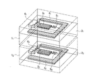
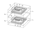
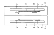
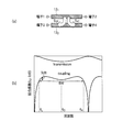
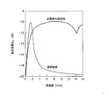
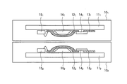
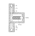
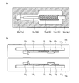
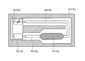
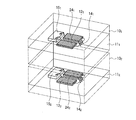
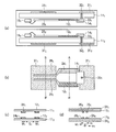
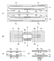
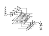
- FIG. 1 is a conceptual perspective view of an inter-module communication device according to an embodiment of the present invention. It is a conceptual perspective view of the communication apparatus between modules of Example 1 of this invention. It is sectional drawing of the communication apparatus between modules of Example 1 of this invention. It is explanatory drawing of the frequency characteristic of the coupler of Example 1 of this invention. It is explanatory drawing of the size of the coupler in Example 1 of this invention, and the relationship of the characteristic of a coupler. It is explanatory drawing of the electromagnetic field analysis simulation result about Example 1 of this invention. It is a conceptual sectional view of a module communication device of Example 2 of the present invention. It is structure explanatory drawing of the communication apparatus between modules of Example 3 of this invention.
- FIG. 18 is an explanatory diagram of frequency characteristics by electromagnetic field simulation for the configuration of the fifth embodiment. It is structure explanatory drawing of the communication apparatus between modules of Example 6 of this invention. It is a conceptual projection top view of the communication apparatus between modules of Example 7 of this invention. It is explanatory drawing of the communication apparatus between modules of Example 8 of this invention. It is a conceptual perspective view of the communication apparatus between modules of Example 9 of this invention.
- FIG. 18 is a configuration explanatory view of an inter-module communication device according to a tenth embodiment of the present invention.
- FIG. 21 is a conceptual cross-sectional view of the inter-module communication device of the twelfth embodiment of the present invention. It is a conceptual sectional view of an inter-module communication device according to a thirteenth embodiment of the present invention.
- FIG. 24 is a configuration explanatory diagram of the inter-module communication device of the fourteenth embodiment of the present invention.
- FIG. 18 is a configuration explanatory view of the inter-module communication device of the embodiment 15 of the present invention. It is a conceptual top view of the module single-piece
- FIG. 24 is a configuration explanatory diagram of the inter-module communication device of the eighteenth embodiment of the present invention. It is a conceptual perspective view of the communication apparatus between modules of Example 19 of this invention. It is characteristic explanatory drawing of the communication apparatus between modules of Example 19 of this invention.
- FIG. 32 is another characteristic explanatory view of the inter-module communication device of the nineteenth embodiment of the present invention.
- FIG. 21 is a configuration explanatory view of a transmission / reception circuit constituting the inter-module communication device of the embodiment 19 of the present invention.
- FIG. 31 is an explanatory diagram of an example of operation waveforms of the transmission and reception circuit forming the inter-module communication device according to the nineteenth embodiment of the present invention. It is explanatory drawing of the measurement result of the frequency characteristic in Example 19 of this invention. It is explanatory drawing of the measurement data of the relationship of a bit error rate (BER) and data transfer speed when data communication is performed using pseudorandom data. It is a conceptual perspective view of the communication apparatus between modules of Example 20 of this invention.
- FIG. 21 is a configuration explanatory view of the inter-module communication device of the embodiment 21 of the present invention. It is a conceptual perspective view of the communication apparatus between modules of Example 22 of this invention.
- 24 is a configuration explanatory diagram of the inter-module communication device of the twenty-third embodiment of the present invention. It is an explanatory view of line width dependence and interval dependence of impedance. It is explanatory drawing of the pattern of the connection part of a coupler and the transmission line for extraction. It is structure explanatory drawing of the data communication between modules using the conventional coil.
- FIG. 1 is a conceptual perspective view of an inter-module communication device according to an embodiment of the present invention, in which two modules 1 1 and 1 2 are arranged close to each other and wirelessly by capacitive coupling and inductive coupling between transmission lines. Perform data communication with
- the semiconductor integrated circuit device 6 1 and 6 2 are connected with a transceiver circuit between.
- the signal lines 3 1, 3 2 and between the feedback signal lines 4 1, 4 2 together are at least partially overlaps the projectively viewed from the lamination direction, the signal lines 3 1, 3 2 each other during and feedback signal line 4 1, 4 2 signal coupling due to capacitive coupling and inductive coupling between the adjacent and in close proximity to the feedback signal coupling occurs laminated.
- the feedback signal coupling is set to be equal to or stronger than the signal coupling.
- the insulating substrate 2 1, 2 2 anything may be an insulating, soft thin about 75 ⁇ m thickness of the substrate, but small devices mounted easily FPC to such as a memory card is suitable, even PCB It may be a semiconductor substrate or a substrate in a package.
- a transmission line can be formed by printing a copper foil having a thickness of about 30 ⁇ m formed on both sides of the substrate and a via that can be routed through the substrate to form a transmission line, and the characteristic impedance of the transmission line is 50 ⁇ Although it is general, make it a value of coupled system impedance.
- FIG. 1 illustrates the case where two modules 1 1 and 12 are close to each other, the number of modules may be three or more. Further, in the case of stacked adjacent modules 1 1, 1 2, may be laminated it remains the same direction, the same surface may be laminated by inverting so as to face. When three or more modules are stacked, they are stacked in the same direction.
- the feedback signal line 4 1, 4 2 to relative signal line 3 1, 3 2 may be made in coplanar structure, or so as to constitute a differential line with the signal line 3 1, 3 2 It is good.
- the resistance to common mode noise is higher than that of the single end, the impedance can be easily controlled, and the design is facilitated because the feedback path of the coplanar structure is not necessarily required.
- the signal line 3 1, 3 2 of the coupling state is varied by the signal line 3 1, 3 2 s intervals or signal line 3 1, 3 2 propagation direction of either the signal of the width of the overlapping of, may be a multi-section coupler, the flat frequency characteristics of the coupling coefficient of the signal line 3 1, 3 2, it is possible to realize a wideband coupler.
- connection between the signal line 3 1, 3 2 and the semiconductor integrated circuit device 6 and 62 may be directly connected, or the signal line 3 1, 3 transmission line 2 from the narrower drawer You may connect using. Since binding of the transmission line between the drawer weaker is desired, or wider than the opposing distance therebetween of signals facing distance line 3 1, 3 2, or, it is desirable to reduce the projective overlap, thereby Since the coupled system impedance of the transmission line is approximately equal to the single characteristic impedance Z 0 , design is facilitated.
- the bandwidth of the communication channel can be made wider (10 Gb / s or more) than that of the conventional inductive coupling, so that the communication can be speeded up.
- the impedance of the communication channel can be configured so as not to change substantially in the range of the communication band and to be uniform with respect to the length. It can be terminated with matched resistors, and the integrated circuit with the transceiver can be placed away from the communication channel, increasing design freedom.
- communication can be speeded up.
- circuit boards when a plurality of circuit boards are vertically arranged, they can be used for wireless data communication without using a conventional connector or wiring connection by a backplane. Alternatively, it can be used for wireless data communication between a module rotating in the device and a module fixed around it.
- FIG. 2 is a conceptual perspective view of the inter-module communication device according to the first embodiment of the present invention
- FIG. 3 is a cross-sectional view thereof.
- the transmission line coupler is composed of rectangular signal lines 12 1 and 12 2 of length L (typically 5 mm) and width W (typically 2 mm).
- Signal feedback path in the coplanar transmission line (return path) 13 1, 13 2 are installed around.
- These signal lines 12 1, 12 2 and the feedback paths 13 1, 13 2 has a thickness which is formed on the substrate 11 1, 11 2 of the surface of the FPC is formed by processing the copper foil of approximately 30 [mu] m.
- the impedance (ratio of voltage to current) of the transmission line does not depend on the location of the line, has almost no dependence on frequency within the target signal band, and is a constant value.
- the value of the characteristic impedance Z 0 to represent "characteristic" of the transmission line is determined by the signal line 12 1, 12 2 and the feedback paths 13 1, 13 2 of the layout, the substrate 11 1, 11 2 of the permittivity and permeability It is decided.
- the impedance of the signal lines 12 1 and 12 2 is influenced by the other signal lines 12 2 and 12 1 by the proximity effect and becomes a value different from Z 0 .
- the proximity effect increases and the impedance of the signal lines 12 1 and 12 2 becomes smaller.
- the impedance of the signal lines 12 1 and 12 2 in the coupled state is herein referred to as a coupled system impedance and represented by Z 0 -coupled .
- a coupled system impedance Conventionally, the characteristic impedance Z 0 is controlled, but in the present invention, the point of controlling the coupled system impedance Z 0 -coupled is essentially different.
- the semiconductor integrated circuit device 15 1 having a transceiver for transmitting and receiving a digital signal signal processing to, 15 2 close to the signal line 12 1, 12 2, for example, when transmitting a digital signal at 10Gb / s is 0.4mm Install at the following distance for wiring connection.
- Output or input impedance of the transceiver, (installed in a semiconductor integrated circuit device 15 1, 15 2, not shown in Figure) coupling system resistance equal to the impedance Z 0-Coupled with the signal line 12 1 is impedance matched with the 12 2.
- the other ends of the signal lines 12 1 and 12 2 and the feedback paths 13 1 and 13 2 are terminated and impedance-matched using resistors 14 1 and 14 2 equal to the coupling system impedance Z 0-coupled . .
- Control of the impedance can also be realized instead of the resistance by adjusting the transconductance g m of the transistor.
- the transconductance gm can be changed according to the voltage between the gate and the source of the transistor, the current flowing to the drain, and the channel shape of the transistor. (Hereinafter, in the case where resistance is described or illustrated, it also includes the case where the transconductance of a transistor is used.)
- the two modules 10 1 and 10 2 may be both fixedly installed and always able to communicate, and may be able to communicate when the modules move and the distance approaches.
- Examples of the former include inter-package communication and inter-board communication.
- Examples of the latter include the case of a noncontact memory card, a probe device over a package, and data communication with a rotating unit.
- the module is sealed with plastic or the like, and an adhesive resin or space may be inserted between the two modules.
- Face the signal line 12 1, 12 2 is disposed may be at the opposite side in the opposite surface of the substrate 11 1, 11 2 of the FPC.
- FIG. 2 has shown the case where it installs in an opposite surface
- FIG. 3 has shown the case where it installs in an opposing surface.
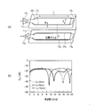
- FIG. 4 is an explanatory diagram of the frequency characteristic of the coupler according to the first embodiment of the present invention, and as shown in FIG. 4A, both terminals of one signal line 121 are terminal 1 and terminal 2, and the other is the signal line 12 2 of the terminals of the terminal 1 and the same side of the pin terminal 3 is referred to the side opposite to the terminal 4.
- a case is considered in which the terminals 2 and 4 are terminated, a signal is input from the terminal 1, and a signal is output from the terminal 3.
- a typical example of the frequency characteristic S 31 of the communication channel signal is transmitted in the transmission line coupling shown in Figure 4 (b).
- the wavelength of the signal lambda, when v and the signal speed of the following formula It is represented by 1).
- the coupling strength is hardly dependent on the frequency and can be transmitted without deformation of the signal waveform, so this area is considered as a signal band .
- f L is approximately 0.5 ⁇ f 0 and f H is approximately 14 ⁇ f 0
- f H ⁇ f L in the signal band is approximately f 0 .
- the communication speed is proportional to the signal band, the smaller the transmission line length (L), the wider the band, and high-speed communication becomes possible.
- the length L of the transmission line coupler is determined from the requirement of the signal band.
- the absolute value C (decibel value) of voltage signal attenuation is given by the following equation (2).
- Z 0 e is the characteristic impedance of the transmission line pair in even mode
- Z 0 o is the characteristic impedance of transmission line pair in odd mode.
- the coupled system impedance of the transmission line pair for the in-phase signal is called even mode impedance (Z 0e ), and the coupled system impedance of the transmission line for the reverse phase signal is called odd mode impedance (Z 0o ).
- even mode since the signal changes in the same phase, the capacitance between the lines is effectively reduced compared to the odd mode in which the signal changes in the opposite phase.
- the even mode impedance (Z 0e ) is larger than the odd mode impedance (Z 0o ). Since (Z 0e -Z 0o ) / (Z 0e + Z 0o ) is a value of 1 or less, the larger the difference, the smaller the value of C and the stronger the coupling strength. Further, the coupling system impedance Z 0 -coupled is determined from Z 0e and Z 0o as shown in the following equation (3).
- the coupler Match the end of the signal line 12 1 , 12 2 by terminating it with a resistance equal to the coupled system impedance Z 0 -coupled or by connecting it to a transmission line having a characteristic impedance Z 0 equal to the coupled system impedance Z 0-coupled.
- the dimensions of the coupler are designed to suppress the reflection of the signal and to increase the coupling strength.
- FIG. 5 shows the results of examining these relationships with an electromagnetic field analysis simulator.
- FIG. 5 (a) is an explanatory view of the width W, interval d and positional deviation s of the signal line
- FIG. 5 (b) is an explanatory view of the line width W and positional deviation S dependency of Z0o and Z0e
- FIG. 5C is an explanatory view of the positional deviation S dependency of the correlation between the voltage signal attenuation C and the line width W.
- the frequency characteristics of the coupler change depending on the wiring width W, and the larger the W, the stronger the coupling.
- the impedances Z 0o and Z 0e of the even mode and the odd mode are respectively the capacitance and inductance between the signal line 12 1 and the feedback path 13 1 , the capacitance and inductance between the signal line 12 2 and the feedback path 13 2 , And the capacitance and inductance between the signal line 12 1 and the signal line 12 2 .
- the feedback path 13 1 and the feedback path 13 coupled between the two is weak, even mode impedance and the odd mode impedance of the coupled transmission line not fixed signal reference potential is not clearly defined. As a result, under actual use conditions, these impedances will fluctuate significantly, making termination difficult.
- a feedback path 13 2 also requires a signal line 12 1, 12 2 between equal to or more binding and.
- the impedance matching is performed based on the coupling system impedance Z 0 -coupled , the reflection of the signal is reduced, and high-speed communication becomes possible, as shown in FIG. A wider wireless communication channel can be realized than in the case of inductive coupling using coils only.
- FIG. Figure 7 is a schematic sectional view of the inter-module communication apparatus according to a second embodiment of the present invention, the substrate 11 1, 11 2 convex member 16 1 on, 16 2 are provided, the signal line so as to extend over the 12 1 and 12 2 are provided, and the other configuration is the same as that of the first embodiment described above.
- the convex members 16 1 and 16 2 in this case are formed of, for example, an ultraviolet curable resin.
- the distance between the signal lines 12 1 and 12 2 gradually changes and becomes closest to the center of the coupler, and the coupling capacitance between the lines becomes growing.
- the difference between the even-mode impedance Z 0o and the odd mode impedance Z 0e increases, bond strength increases.
- the signal strength on the receiving side can be increased.
- the coupling strength varies depending on the place, and their superposition becomes the coupling coefficient C total (f) of the entire coupled transmission line as shown in the following equation (4).
- the band of the coupled transmission line can be increased by adjusting C (x) which is a function of the position so that C total (f) becomes flat.
- C (x) which is a function of the position so that C total (f) becomes flat.
- the coupling coefficient between the transmission lines can be increased by shortening the communication distance, and the S / N ratio on the receiver side can be increased.
- the strength of the coupling coefficient which changes continuously the frequency characteristic of the coupling coefficient of the transmission line can be made flat and the frequency band can be expanded.
- a feedback path to be described later includes a signal line and a differential line.
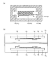
- FIG. 8A is a conceptual plan view of a single module
- FIG. 8B is a conceptual cross-sectional view of the inter-module communication device of the third embodiment of the present invention.
- the feedback paths 13 1 and 13 2 are formed on both left and right sides of the signal lines 12 1 and 12 2 in the signal transmission direction of the coupler so as to be line symmetrical with respect to the coupler. Do.
- Example 3 of the present invention since the feedback path is symmetrical on both sides of the signal line 12 1, 12 2, current flowing toward the other end B from one end A of the signal line 12 1, 12 2, Since return from the other end B to one end A through the feedback paths on both sides of the signal lines 12 1 and 12 2 , two coils of the same shape are arranged side by side, and the current flows in the opposite direction there Will be the same.
- FIG. Fig.9 (a) is a conceptual top view of a module single-piece
- FIG.9 (b) is a conceptual sectional view of the communication apparatus between modules of Example 4 of this invention.
- the substrate 11 1, 11 blocking layer 17 1 so as to include the coupler 2 of the back surface, 17 is 2 which was provided.
- the blocking layer 17 1, 17 2 are formed by a copper foil which is formed on the other surface of the substrate 11 1, 11 2 of the FPC.
- the coupler and the semiconductor integrated circuit device 15 1, 15 2 in the figure are arranged on the same plane, a semiconductor integrated circuit device 15 1, 15 2 may be disposed on the opposite side using the via .
- the blocking layers 17 1 and 17 2 reduce the penetration of electromagnetic field noise from the outside into the coupler. As a result, noise immunity is enhanced. Conversely, the influence of radio communication using the coupler reduces external electromagnetic radiation (that is, electromagnetic interference) by the blocking layer. As a result, electromagnetic compatibility is enhanced. Such a configuration is also applied to the case where a feedback path to be described later includes a signal line and a differential line.
- FIG. Fig.10 (a) is a conceptual perspective view of the coupler of the inter-module communication apparatus of Example 5 of this invention
- FIG.10 (b) is a conceptual top view
- FIG.10 (c) is a coupling
- a wider band coupler can be realized by changing the line widths of the signal lines 12 1 and 12 2 uniformly. That is, a plurality of couplers of different widths may be connected to form multiple nodes.
- the wiring width is changed, it becomes difficult to control the wiring impedance to a constant value, which causes multiple reflections of the signal. Therefore, in the fifth embodiment of the present invention, while the line width is kept constant and the impedance is controlled to be constant, the portions where the signal lines 12 1 and 12 2 overlap and are coupled become multi-nodes and the line widths are different. Bent the transmission line coupler.
- FIG. 11 is an explanatory diagram of a frequency characteristic by electromagnetic field simulation for the configuration of the fifth embodiment, and a signal band of 12.6 GHz and a coupling strength S 31 of 14.5 dB can be realized.
- the coupling capacitance between the lines increases as the overlapping portion is larger.
- the difference between the even mode and the odd mode impedances Z 0o and Z 0e becomes large, and the coupling strength C becomes large.
- the strength of the signal coupled at the node and transmitted to the receiving end is given by the following equation (5) in consideration of the change in phase.
- the length of each node is L
- the velocity and frequency of the signal are v and f, respectively
- ⁇ 2 Lf / v.
- the total coupling coefficient C total is a superposition of signals transmitted from each node to the receiving end, and therefore, is represented by the following equation (6).
- the band of the coupled transmission line can be increased by adjusting the coupling strength of each node so that C n and C total (f) become flat.
- the frequency characteristic of the coupling coefficient can be made flat and a wide band coupler can be realized by the same idea even when the transmission line is configured by a curved surface.
- the signal lines 12 1 and 12 2 have multiple nodes, it is possible to realize a coupled communication path that is wider than a single-node coupler. Such a configuration is also applied to the case where a feedback path to be described later includes a signal line and a differential line.
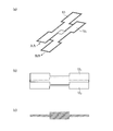
- FIG. 12 (a) is a conceptual plan view of one signal line of the inter-module communication device of the sixth embodiment of the present invention
- FIG. 12 (b) is a conceptual plan view of the other signal line
- 12 (c) is an explanatory view of a connecting portion.
- the signal lines 12 1 and 12 2 are curved in a curvilinear manner to realize the number of nodes as another realization method of the multi-joint coupler. Is a great deal.
- the coupling point changes continuously and little by little, the rapid change in the impedance is small, and a wider band can be achieved.
- a feedback path to be described later includes a signal line and a differential line.
- FIG. 13 is a conceptual projection plan view of the inter-module communication device of the seventh embodiment of the present invention. As shown in FIG. 13, the signal lines 12 1 and 12 2 intersect with each other to form a coupler at the intersection.
- the width of the intersection becomes wider at the center of the intersection and becomes narrower at both sides. Furthermore, even if the relative position of the signal lines 12 1 and 12 2 deviates in any direction of the plane, the shape of the intersection portion is constant, so that the coupling characteristic is constant regardless of the positional deviation of the module.
- Example 7 of the present invention since the arrangement by intersecting the signal lines 12 1, 12 2 obliquely, can be realized broadband wireless communication path. Further, even if shift module 10 1, 10 2 of the relative position has a feature that the characteristics of the communication channel does not change. Such a configuration is also applied to the case where a feedback path to be described later includes a signal line and a differential line.
- FIG. 14 is an explanatory diagram of the inter-module communication device of the eighth embodiment of the present invention, and shows two modules as a plan view. As shown in FIG., It is obtained by combining a plurality of signal line 12 2, 12 3 provided on the single signal line 12 1 and the other modules 10 2 provided on one module 10 1.
- Signal transmitted from the semiconductor integrated circuit device 15 1 of the module 10 1 may transmit simultaneously module 10 2 of the semiconductor integrated circuit device 15 2 and the semiconductor integrated circuit device 15 3.
- coupler which is not connected to the semiconductor integrated circuit device where not used for binding, i.e., by providing the dummy coupler 20, and the impedance of the signal line 12 1 constant coupling system impedance Z 0-Coupled Control can be facilitated.
- the other module 10 2 is provided with two couplers may be provided three or more couplers.
- the eighth embodiment of the present invention since a plurality of couplers are provided in one module, it is possible to realize coupled communication branched into a plurality of transmission lines by one transmission line, and a plurality of them from one semiconductor integrated circuit chip Data can be communicated to the semiconductor integrated circuit chip of Such a configuration is also applied to the case where a feedback path to be described later includes a signal line and a differential line.
- FIG. 15 is a conceptual perspective view of the inter-module communication device of the ninth embodiment of the present invention.
- the signal lines 12 1 and 12 2 are connected to the semiconductor integrated circuit devices 15 1 and 15 2 by transmission lines 18 1 and 18 2 of characteristic impedance Z 0 equal to the coupling system impedance Z 0-coupled of the signal lines 12 1 and 12 2 ing.
- the transmission line 18 1, 18 2 parts of a semiconductor integrated circuit device 15 1, 15 2 and the signal line 12 1, 12 for lead lines connecting 2 It is desirable not to combine them.
- the transmission lines 18 1 and 18 2 use a line width thinner than the coupling portion.
- the line widths of the signal lines 12 1 and 12 2 are 2 mm, whereas the line widths of the transmission lines 18 1 and 18 2 are 0.3 mm.
- the shape of the feedback paths 13 1 and 13 2 is also different from that of the first embodiment.
- the coupled system impedance Z 0 -coupled of the transmission lines 18 1 and 18 2 for drawing out is the characteristic impedance Z 0.
- the signal line 12 1, 12 2 of the coupling system impedance Z 0-Coupled for example a 50 [Omega, the signal line 12 1, 12 2 characteristic impedance Z 0 of itself is higher than 50 [Omega, the transmission line 18 1 of the lead-out,
- the characteristic impedance Z 0 of 18 2 is designed to be 50 ⁇ .
- the semiconductor integrated circuit device 15 1, 15 2 provided with a transceiver on the signal line 12 1, 12 2 of the most recent (e.g. within 0.4 mm) since the transmission lines 18 1 and 18 2 for drawing out are provided, the semiconductor integrated circuit devices 15 1 and 15 2 provided with the transceiver are separated from the signal lines 12 1 and 12 2. But because it can be installed, the freedom of design is increased.
- FIG. 16 (a) is a conceptual cross-sectional view of the inter-module communication device according to the tenth embodiment of the present invention
- FIG. 16 (b) is a conceptual plan view
- FIG. 16 (c) is FIG. 16 (d) is a cross-sectional view taken along the alternate long and short dash line connecting BB 'in FIG. 16 (b).
- Example 10 is obtained by employing the microstrip structure instead of the coplanar structure of Example 9, the provided substrate 111, plane 31 on the rear surface of 11 2 1, 31 2, via 32 1, 32 2 And the lands 33 1 and 33 2 are connected to the resistors 14 1 and 14 2 .
- planes 31 1 and 31 2 are generally grounded ground planes, but they need not necessarily be grounded.
- the so the width W 1 of the signal line 12 1, 12 2 are narrower than the transmission line 18 1, 18 2 of width w 1, below As described in detail in Example 23, the degree of coupling of the coupler can be increased.
- FIG. 17 is a conceptual projected plan view of the inter-module communication device of the eleventh embodiment of the present invention.
- the transmission line 18 1, 18 2 for drawer so hardly bind between the module 10 1, 10 2, module 10 1 and the module 10 and second lead-out transmission line 18 1, 18 2
- the extending directions were opposite to each other.
- the transmission line 18 1, 18 2 of the little binding for the drawer the transmission lines 18 1, 18 2 of the coupling system impedance Z 0-Coupled for drawer is equal to the characteristic impedance Z 0, therefore, the signal line 12 1 , by designing the transmission line 18 1, 18 2 of the characteristic impedance of drawer to be equal to the bond system impedance Z 0-coupled of 12 second coupling portion, the reflection of the signal does not occur.
- FIG. 18 is a conceptual cross-sectional view of the inter-module communication device of the twelfth embodiment of the present invention.
- the transmission line 18 1 of the lead-out, 18 2 is so hardly bind between the module 10 1, 10 2, the substrate 11 in the signal line 12 1, 12 2 with through-vias 19 1, 19 2 1, 11 transmission lines 18 1 for drawer 2, 18 2 formed on the surface opposite to the surface provided with the signal line 12 1, 12 2 each other to place the module 10 1 and the module 10 2 to face
- the feedback paths 13 1 and 13 2 are also provided on the same plane as the lead-out transmission lines 18 1 and 18 2 .
- Example 12 of the present invention since elements such as couplers become signal lines 12 1, 12 semiconductor integrated circuit device 2 to the substrate surface provided with 15 1, 15 2, resistors 14 1, 14 2 is absent
- the signal lines 12 1 and 12 2 can be disposed closer to each other to strengthen the coupling, and the transmission lines 18 1 and 18 2 for extraction can be disposed farther to each other to weaken the coupling.
- a feedback path to be described later includes a signal line and a differential line.
- FIG. 19 is a conceptual cross-sectional view of the inter-module communication device of the thirteenth embodiment of the present invention.
- the substrate 11 1 of both modules 10 1, 10 2, 11 2 are arranged in the same direction.
- to shorten the distance between the signal line 12 1, 12 2 in order to increase the distance between the transmission lines 18 1, 18 2 for drawers, provided with a three-dimensional structure 21 in the module 10 2 lower, and lifting the signal line 12 2.
- the signal lines 12 1 and 12 2 are arranged closer to each other in a state in which the directions of the substrates 11 1 and 11 2 are the same to strengthen the coupling, and the transmission line 18 for drawing out. 1 , 18 2 can be placed further apart to weaken the bond.
- a feedback path to be described later includes a signal line and a differential line.
- FIG. 20 (a) is a conceptual plan view of a single module
- FIG. 20 (b) is a conceptual cross-sectional view of the inter-module communication device of the fourteenth embodiment of the present invention.
- Example 14 of the present invention, the substrate 11 1, 11 2 and the laminate in the same direction, blocking layer in a position to cover the transmission line 18 1 of module 10 first substrate 11 1 of the rear surface of the drawer being disposed on the upper side 22 One is provided.
- Example 14 of the present invention since there is provided a blocking layer 22 1, the substrate 11 1, 10 without the need for vias and conformation 2, the semiconductor integrated circuit device 15 1, 15 2 and the transmission line 18 1 , 18 2 and the signal line 12 1, 12 2, it can impedance at its end is aligned, thus, not reflected signals occur, it can be high-speed communication with high reliability.
- a feedback path to be described later includes a signal line and a differential line.
- FIG. 21 is a conceptual plan view of a single module
- FIG. 21 (b) is a conceptual cross-sectional view of the inter-module communication device of the fifteenth embodiment of the present invention.
- the side surfaces of the junctions between the transmission lines 18 1 and 18 2 for extraction and the signal lines 12 1 and 12 2 are curved.
- the side surfaces of the junctions between the transmission lines 18 1 and 18 2 and the signal lines 12 1 and 12 2 are curved, abrupt changes in impedance are eliminated and the impedance is as uniform as possible. I have to.
- the impedance is substantially uniform, the reflection of the signal can be reduced and a broadband coupler can be realized.
- a feedback path to be described later includes a signal line and a differential line.
- FIG. 22 is a conceptual plan view of a single module. As shown, also provided a transmission line 18 3 (18 4) to the signal line 12 1 (12 2) and the other end, the transmission line 18 3 (18 4) to the terminating impedance matching circuit 23 1 (23 2) It is connected to the built-in semiconductor integrated circuit device 15 1 (15 2 ). If the semiconductor integrated circuit chip can be placed in the immediate vicinity of the coupler, both may be connected by direct wiring without passing through the transmission line.
- All or part of the impedance matching function is mounted in the semiconductor integrated circuit device 15 1 (15 2), and to be able to adjust the impedance. If the value of the matching impedance is fixed, impedance mismatch will occur if the coupling system impedance Z 0 -coupled changes due to manufacturing variations in parameters such as line widths of coupled transmission lines, or fluctuations in the distance between the lines. , The coupling coefficient decreases. The signal reflection or the like is monitored to detect the value of Z 0 -coupled , and the termination impedance is adaptively adjusted according to the change.
- Figure 23 is an illustration of an example of a termination impedance control circuit, the semiconductor integrated circuit device 15 1 of the module 10 2, the output impedance is connected variable transmitter to the signal line 12 2.
- Identical replica transmission circuit are mounted, it is connected to the adjustable termination resistor identical replica termination resistor and connecting the other end of the signal line 12 2.
- a pattern (0011 0011... Etc.) corresponding to the frequency at which the coupling coefficient of the transmission line becomes maximum is output from the transmitter, and the output signals of the transmitter and the replica transmitter at that time are monitored.
- the output of the transmitter and the output signal level of the replica transmitter have the same value.
- This value is detected by, for example, a peak detection circuit, compared by a comparator, and the value of R t is changed so that the two coincide.
- the termination of the other end of the transmission line is also set to the same value.
- the value of the variable termination resistor at the other end is set using the low speed communication mode or the like.
- R t at which both coincide is held in a register or the like, and this set value is used thereafter. If resistance control is performed by operating the monitor circuit also at the time of communication, the communication distance may vary, and an optimum termination resistance value can be maintained even when the impedance of the transmission line changes.
- Example 15 of the present invention since the provided terminal impedance adjusting circuit 23 1, 23 2, impedance manufacturing variations coupling line, it is varied by variation of the line distance, impedance matching Since it can be obtained, signal reflection can be prevented and high-speed communication can be performed.
- the transmission line 18 1 if installed semiconductor integrated circuit device 15 1, 15 2 in the immediate vicinity of the signal line 12 1, 12 2, 18 2 may be connected to each other in a direct line without intervention. Such a configuration is also applied to the case where a feedback path to be described later includes a signal line and a differential line.
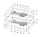
- FIG. 24 is a conceptual perspective view of the inter-module communication device of the seventeenth embodiment of the present invention.
- transmission lines 18 5 and 18 6 are provided at the other ends of the signal lines 12 1 and 12 2 , respectively, and connected to the semiconductor integrated circuit devices 15 5 and 15 6 . Take impedance matching.
- the current (reverse current) flowing from terminal 4 to the other terminal of the other coupler is compared with the current (forward current) flowing from terminal 3 to terminal 4 If the signal is sufficiently large, for example, if it is 100 times larger, the signal inputted from the terminal 1 can be outputted from the terminal 3 at the same time as the signal inputted from the terminal 2 can be outputted from the terminal 4
- the coupler can form two independent communication paths. At the same time as the signal inputted from the terminal 1 is outputted from the terminal 3, the signal inputted from the terminal 4 can also be outputted from the terminal 2.
- S 31 / s 41 When S 31 / s 41 is referred to as a separation factor, when the separation factor S 31 / s 41 can not be made sufficiently large, two main causes are considered. One is the reflection of the signal. If the impedance matching is made more perfect, the separation coefficient S 31 / s 41 can be increased. The second is the difference in signal propagation delay in the even mode and the odd mode.
- the separation factor can be increased by making the dielectric constants of the materials as uniform as possible.
- the data communication rate can be doubled.
- FIG. 25 (a) is a conceptual cross-sectional view of the inter-module communication device of the eighteenth embodiment of the present invention
- FIG. 25 (b) is a conceptual plan view
- FIG. 25 (c) is FIG. 25 (d) is a cross-sectional view along the alternate long and short dash line connecting BB 'in FIG. 25 (b).
- Example 18 is obtained by employing the microstrip structure instead of the coplanar structure of Example 17, it is provided with a substrate 11 1, 11 plane 31 1 on the back surface of the 2, 31 2.
- planes 31 1 and 31 2 are generally grounded ground planes, but they need not necessarily be grounded.
- FIG. 26 is a conceptual perspective view of the inter-module communication device of the nineteenth embodiment of the present invention.
- the feedback paths 24 1 and 24 2 have the same configuration as the signal lines 12 1 and 12 2 to form a differential coupler. Also in this case, the feedback paths 24 1 and 24 2 and the signal lines 12 1 and 12 2 are terminated by the resistors 14 1 and 14 2 having the characteristic impedance Z 0 equal to the coupled system impedance Z 0-coupled .
- the differential impedance Z diff is approximately 100 ⁇ .
- the two lines, ie, the feedback paths 24 1 and 24 2 and the signal lines 12 1 and 12 2 are far apart and typically do not couple apart by more than three times the line width, then 100 ⁇ .
- it is slightly smaller than 100 ⁇ , typically about 10% smaller.
- the communication distance is 1 mm.
- the coupling coefficient C is high when the width is 0.5 mm and the distance is 1.5 mm to 2.5 mm, and the band (3-dB BW) is also wide.
- the impedance is about 100 ⁇ and the differential impedance is about 200 ⁇ .
- the dimensions of the transmission line coupler are determined by design target values such as impedance, coupling coefficient and band, and physical property values such as the material of the substrate.
- the termination resistance is, for example, a component having a size of about 1.6 mm ⁇ 0.8 mm, so when the transmission coupler interval is 1.5 mm to 2.5 mm, the transmission coupler end is gently bent to Make it easy to connect with the termination resistance by about 1.6 mm. In addition, if it bends rapidly, impedance will not become uniform and it is not desirable.
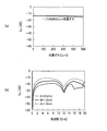
- FIGS. 27 and 28 are diagrams for explaining the characteristics of the inter-module communication device of the nineteenth embodiment of the present invention.
- FIG. 27 (a) is an equivalent circuit diagram of the inter-module communication device of the nineteenth embodiment of the present invention, and in this case, the couplers, ie, the widths W of the feedback paths 24 1 and 24 2 and the signal lines 12 1 and 12 2 are shown. Is 0.5 mm, the spacing S is 1.5 mm, and the distance d is 1 mm.
- FIG. 27 (b) is an explanatory view of the coupler length dependency of the frequency characteristic of the coupling coefficient S 31.
- the coupling coefficient S 31 when the length L of the coupler is 4 mm, 6 mm, and 10 mm, respectively.
- the result of actually measuring As shown in the figure, when L is shortened, the center frequency increases in inverse proportion to L, and the band becomes wider in proportion to the center frequency.
- FIG. 28 (a) is a positional deviation-dependent illustration of coupler frequency characteristics of the coupling coefficient S 31, as shown in figure, the coupling coefficient when shifted in the direction shown in FIG. 27 (a) is It hardly changes. From these facts, it can be understood that the modules can communicate with each other even if the relative position of the modules changes.
- FIG. 28 (b) is an explanatory view of the distance d dependency of the coupler on the frequency characteristic of the coupling coefficient S 31.
- the width W of the coupler is 0.5 mm
- the distance S is 1.5 mm
- the length L is 6 mm. It shows the results of measurement of the coupling coefficient S 31 when the distance d is respectively 0.5 mm, 1 mm and 1.5 mm.
- the coupling coefficient S 31 is decreased, but the band is hardly changed. Therefore, by adjusting the gain of the amplifier at the input stage of the receiver according to the communication distance, communication can be performed at the same speed even if the distance changes.
- FIG. 29 is an explanatory diagram of the configuration of the transmission / reception circuit that configures the inter-module communication device according to the nineteenth embodiment of the present invention
- FIG. 30 is an explanatory diagram of an example of operation waveforms.
- the received signal is amplified by a wideband low noise amplifier, and then the original signal is restored through a hysteresis comparator.
- integration may be performed using an integration circuit at the receiver.
- integration may be performed by combining the transmitter and the receiver.
- the integration operation may be performed by an analog circuit or digital signal processing.
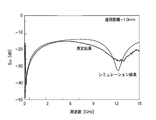
- FIG. 31 is an explanatory diagram of measurement results of frequency characteristics in Example 19 of the present invention, and frequency characteristics almost equal to simulation results were obtained.
- FIG. 32 is an explanatory diagram of measured data of a relationship between a bit error rate (BER) and a data transfer rate when data communication is performed using pseudo random data, and the configuration of the nineteenth embodiment enables high reliability. It is understood that high-speed data communication can be performed.
- BER bit error rate
- the differential configuration is more tolerant to common mode noise than single end.
- the coupling system impedance Z 0 -coupled can be easily controlled and there is no need for a feedback path, the design is simple.
- one of the differential lines is a signal path and the other is a feedback path.
- a feedback path may be provided.
- FIG. 33 is a conceptual perspective view of the inter-module communication device of the twentieth embodiment of the present invention.
- the transmission lines 25 1 25 2 26 1 26 2 are provided for all of the signal lines 12 1 12 2 and the feedback paths 24 1 24 2 .
- the semiconductor integrated circuit device 15 1, 15 2 and the transmission line 25 1, 25 2, 26 1, 26 2 and the signal line 12 1, 12 2 and the return path 24 1, 24 2 is connected to each impedance matching
- the ends of the signal lines 12 1 and 12 2 and the feedback paths 24 1 and 24 2 are also impedance matched.
- the transmission line 25 1, 25 2, 26 1, 26 2 is the signal line 12 1 , 12 2 and or using the feedback path 24 1, 24 2 from the thin line width, or so as not to be disposed in the projection the same position when viewed from the laminating direction, to desirably laid away respective transmission lines.
- the differential transmission lines are closely coupled, and typically, the transmission lines 25 1 , 25 2 , 26 1 and 26 2 are disposed with a spacing of within three times the width and coupled.
- feedback paths may be separately provided, for example, in parallel next to the transmission lines 25 1 25 2 26 1 26 2 or on the opposite side of the FCB.
- the transmission lines 25 1 , 25 2 , 26 1 and 26 2 for drawing out are provided, a semiconductor integrated circuit device 15 provided with a transceiver in addition to the effect by the differential characteristics.
- the first and second 152 can be installed even away from the signal lines 12 1 and 12 2 and the feedback paths 24 1 and 24 2 , the degree of freedom in design is increased.
- FIG. 34 is a conceptual cross-sectional view of the inter-module communication device of the twenty-first embodiment of the present invention
- (b) of FIG. 34 is a conceptual plan view
- (c) of FIG. 34 (d) is a cross-sectional view along the alternate long and short dash line connecting BB 'in FIG. 34 (b).
- embodiment 20 is obtained by employing the microstrip structure, the substrate 11 1, 11 plane 31 1 on the back surface of the 2, 31 2 provided, via 32 1, 32 2 and the lands 33 1, It is connected to the resistors 14 1 and 14 2 via the resistor 33 2 .
- the planes 31 1 and 31 2 are generally grounded ground planes, but they need not necessarily be grounded.
- the signal line 12 1, 12 2 and the return path 24 1, 24 2 of the width W 1 transmission line 25 1, 25 2, 26 1, 26 Since the width is made smaller than the width w 1 of 2, the degree of coupling of the coupler can be increased as will be described in detail in Example 23 described later. Further, since wider than the signal line 12 1, 12 2 and the feedback paths 24 1, 24 2 of the spacing S 1 transmission line 25 1, 25 2 and the transmission line 26 1, 26 2 of the spacing s 1, this point However, the coupling degree of the coupler can be increased.
- FIG. 35 is a conceptual perspective view of the inter-module communication device of the twenty-second embodiment of the present invention.
- transmission lines 25 3 25 4 26 3 26 4 for extraction are provided at the other ends of the signal lines 12 1 12 2 and the feedback paths 24 1 24 2 , respectively.
- the semiconductor integrated circuit devices 15 5 and 15 6 are connected to the transmission lines 25 3 25 4 26 3 26 4 .
- the data communication speed can be doubled.
- FIGS. 36 (a) is a conceptual cross-sectional view of the inter-module communication device according to the twenty-third embodiment of the present invention
- FIG. 36 (b) is a conceptual plan view
- FIG. 36 (c) is FIG. 36 (b).
- 36 (d) is a cross-sectional view along the alternate long and short dash line connecting BB 'in FIG. 36 (b).
- Example 23 is obtained by employing the microstrip structure in Example 22, the substrate 11 1, 11 provided with a plane 31 1, 31 2 to 2 of the back, the signal line 12 1, 12 2 and the feedback path 24 1, 24 2 of the spacing S 1 wider than the transmission line 25 1, 25 2, 25 3, 25 4 and the transmission line 26 1, 26 2, 26 3, spacing s 1 26 4
- the planes 31 1 and 31 2 are generally grounded ground planes, but they need not necessarily be grounded.
- the signal lines 12 1 and 12 2 and the feedback path 24 1 are connected to the transmission lines 25 1 25 2 25 3 25 4 25 1 26 2 26 3 26 4 for connection to the differential coupler.
- 24 2 intervals that are tightly coupled to the case, an interval is arranged within three times the width attached sparsely disposed than 3 times the width. If they are loosely coupled, they need to be placed on planes 31 1 and 31 2 as shown in order to define the characteristic impedance of the differential mode of the line.
- the distance (t) between the planes 31 1 and 32 2 and the transmission lines 25 1 25 2 25 3 25 4 26 1 26 2 26 3 26 4 is typically about 0.02 mm (flexible substrate ) To about 0.1 mm (in the case of the FR4 circuit board). If the characteristic impedance of the differential for example, 100 [Omega (corresponding to 50 ⁇ in each line single phase), the line width w 1 and the spacing s 1 is typically on the order of 0.1 ⁇ 0.4 mm.
- Signal lines 12 1 and 12 2 constituting a coupler with the transmission lines 25 1 25 2 25 3 25 4 25 1 26 2 26 3 26 4 for extraction, and the feedback paths 24 1 24 2
- the characteristic impedance Z ver of the coupler portion is expressed by the following equation (7) similarly to the above equation (3) using the even mode impedance (Z even, ver ) and the odd mode impedance (Z odd, ver ).
- the differential characteristic impedance Z ver of the coupler portion is also 100 ⁇ (single Set Z even, ver and Z odd, ver so that the phase becomes 50 ⁇ ).
- FIG. 37 is an explanatory view of the line width dependency and the space dependency of the impedance
- FIG. 37 (a) is an explanatory view of the line width dependency and the space dependency of the even mode impedance Z even
- 37 (b) is an explanatory view of the line width dependency and interval dependency of the odd mode impedance Z odd, ver .
- the signal line 12 1, 12 2 and the return path 24 1, 24 between two of A broad line width W 1 and the spacing S 1 constant line capacitance becomes greater, Z the even, ver, Z Both odd and ver decrease. Also, if a wider spacing S 1 and the line width W 1 constant, capacitance decreases with an increase in distance between lines facing diagonally, and because the area is increased magnetic flux is formed, Z the even, ver, Z odd, ver increases.
- the degree of coupling between the couplers is expressed by the following equation (8) as in the case of the above equation (2). Therefore, the coupling can be strengthened by increasing the difference between Z even and ver and Z odd and ver .
- W 1 and s 1 are taken wider, the degree of coupling can be further increased, but the size of the coupler increases and the mounting efficiency deteriorates, and the frequency band changes depending on the length direction of the coupler There is an upper limit to W 1 and s 1 for reasons such as.
- the wider the line width or the spacing the less susceptible to the alignment error of the joint, and typically, W 1 > 0.3 mm is required.
- the degree of coupling can be increased by designing so as to satisfy W 1 1w 1 .
- the distance S 1 of the coupler is larger than the line width W 1, it can be easily designed because the differential coupling is sparse. In particular, it is desirable that the spacing S 1 be twice or more of the line width W 1 because coupling becomes sparse enough. On the other hand, when the distance S 1 is greater than or equal to 3 times the line width W 1, how much effect on the impedance eliminated apart a distance S 1.
- Figure 38 is a transmission line 25 1 of the signal line 12 1, 12 2 and the return path 24 1, 24 2 and drawer constituting the coupler, 25 2, 25 3, 25 4, 26 1, 26 2, 26 3 is an explanatory view of the pattern of the connecting portion 26 4, the same effect in any case will be obtained.
- Embodiments 17 to 19 of the differential configuration Embodiment 2, Embodiment 4, Embodiment 5, Embodiment 6, Embodiment 7, Embodiment 8 and Embodiment 8 are provided.
- the configurations of the tenth embodiment, the eleventh embodiment, the twelfth embodiment, the thirteenth embodiment, the fourteenth embodiment or the fifteenth embodiment may be combined as appropriate.
Landscapes
- Engineering & Computer Science (AREA)
- Computer Networks & Wireless Communication (AREA)
- Signal Processing (AREA)
- Near-Field Transmission Systems (AREA)
- Semiconductor Integrated Circuits (AREA)
- Transceivers (AREA)
- Dc Digital Transmission (AREA)
- Production Of Multi-Layered Print Wiring Board (AREA)
- Power Engineering (AREA)
Abstract
Description






なお、半導体集積回路チップを結合器の直近に設置できれば伝送線路を介さずに直接配線で両者を接続しても良い。


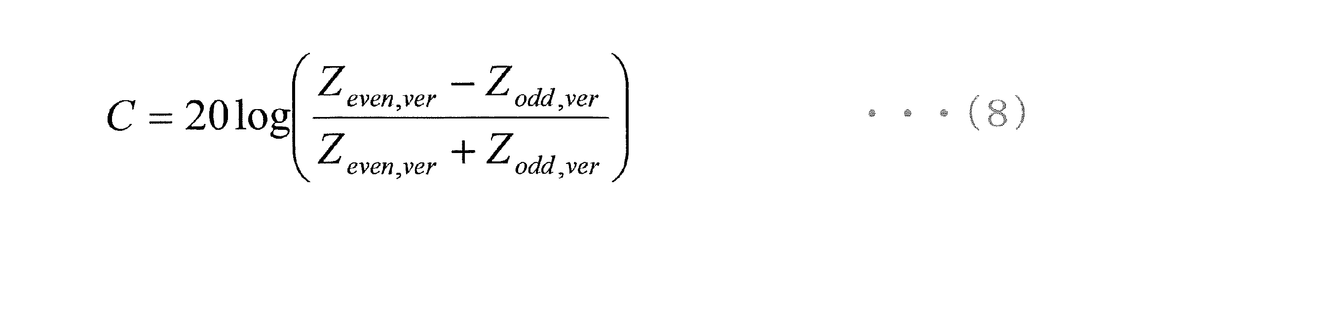
Claims (38)
- 特性インピーダンスがZ01のインピーダンスを有する第1信号線路と、
前記第1信号線路の帰還経路を提供する第1帰還信号線路と
前記第1信号線路と前記第1帰還信号線路とを終端する第1終端部材と、
送受信回路を備えた第1半導体集積回路装置と
を少なくとも有する第1モジュールと、
特性インピーダンスがZ02のインピーダンスを有する第2信号線路と、
前記第2信号線路の帰還経路を提供する第2帰還信号線路と
前記第2信号線路と前記第2帰還信号線路とを終端する第2終端部材と、
送受信回路を備えた第2半導体集積回路装置と
を少なくとも有する第2モジュールとを、
互いに対向させて近接配置されるとともに、
前記第1終端部材及び前記第2終端部材のインピーダンスが、前記Z01及びZ02とは異なる前記第1モジュールと前記第2モジュールとの結合状態における近接効果を反映した結合系インピーダンスであることを特徴とするモジュール間通信装置。 - 前記第1信号線路が、第1絶縁性基板上に設けられた信号波長の1/10以上の長さを有する信号線路であり、
前記第1半導体集積回路装置が前記第1信号線路と前記第1帰還信号線路とに接続され、
前記第2信号線路が、第2絶縁性基板上に設けられた信号波長の1/10以上の長さを有する信号線路であり、
前記第2半導体集積回路装置が、前記第2信号線路と前記第2帰還信号線路とに接続され、
前記第1信号線路と前記第2信号線路とがその少なくとも一部が積層方向から見て投影的に重なり、且つ、
前記第1帰還信号線路と前記第2帰還信号線路とがその少なくとも一部が積層方向から見て投影的に重なり、
前記第1信号線路と前記第2信号線路の間に容量結合および誘導結合を用いて信号結合が生じ、前記第1帰還信号線路と第2帰還信号線路の間に容量結合および誘導結合を用いて帰還信号結合が生じ、
前記信号結合によって前記第2信号線路に前記第1信号線路の信号が伝送されるように積層することを特徴とする請求項1に記載のモジュール間通信装置。 - 前記帰還信号結合が前記信号結合と同じもしくはそれよりも強いことを特徴とする請求項2に記載のモジュール間通信装置。
- 前記第1帰還信号線路が前記第1信号線路に対してコプレーナ構造を形成し、
前記第2帰還信号線路が前記第2信号線路に対してコプレーナ構造を形成することを特徴とする請求項2に記載のモジュール間通信装置。 - 前記第1帰還信号線路が前記第1信号線路の両側に対して対称構造を有し、
前記第2帰還信号線路が前記第2信号線路の両側に対して対称構造を有することを特徴とする請求項4に記載のモジュール間通信装置。 - 前記第1絶縁性基板の前記第1信号線路を配置した面と反対側の面に第1電磁シールド層を有し、
前記第2絶縁性基板の前記第2信号線路を配置した面と反対側の面に第2電磁シールド層を有することを特徴とする請求項2に記載のモジュール間通信装置。 - 前記第1信号線路と前記第2信号線路との間隔或いは前記第1信号線路と前記第2信号線路との重なりの幅のいずれかが信号の伝搬方向で異なることにより前記第1信号線路と前記第2信号線路との結合状態が前記信号の伝搬方向で異なることを特徴とする請求項2に記載のモジュール間通信装置。
- 前記第1モジュール或いは第2モジュールの一方が、前記第1信号線路或いは第2信号線路に対して、ダミー結合器を挟んで、第3信号線路及び前記第3信号線路の帰還経路を提供する第3帰還信号線路とを有し、
前記第3信号線路と前記第3帰還信号線路とを終端する第3終端部材と、
前記第3信号線路と前記第3帰還信号線路とに接続された送受信回路を備えた第3半導体集積回路装置と
を有することを特徴とする請求項2に記載のモジュール間通信装置。 - 前記第1信号線路が、前記第1モジュールと前記第2モジュールとの結合状態における近接効果を反映した結合系インピーダンスを有する第1引き出し用伝送線路を介して前記第1半導体集積回路装置と接続し、
前記第2信号線路が、前記結合系インピーダンスを有する第2引き出し用伝送線路を介して前記第2半導体集積回路装置と接続していることを特徴とする請求項2に記載のモジュール間通信装置。 - 前記第1絶縁性基板の前記第1信号線路を配置した面と反対側の面に少なくとも第1信号線路に対向する部分が欠落部となっている第1のプレーンを有し、
前記第2絶縁性基板の前記第2信号線路を配置した面と反対側の面に少なくとも第2信号線路に対向する部分が欠落部となっている第2のプレーンを有することを特徴とする請求項9に記載のモジュール間通信装置。 - 前記第1信号線路の線幅が、前記第1引き出し用伝送線路の線幅より大きいか或いは等しく、
前記第2信号線路の線幅が、前記第2引き出し用伝送線路の線幅より大きいか或いは等しいことを特徴とする請求項9に記載のモジュール間通信装置。 - 前記第1信号線路と前記第2信号線路が積層方向からみて互いに整列した状態において、前記第1引き出し用伝送線路と前記第2引き出し用伝送線路とが互いに異なった方向に延在していることを特徴とする請求項9に記載のモジュール間通信装置。
- 前記第1引き出し用伝送線路と前記第2引き出し用伝送線路との対向間隔が、
前記第1信号線路と前記第2信号線路との対向間隔より広いことを特徴とする請求項9に記載のモジュール間通信装置。 - 少なくとも前記第1絶縁性基板の前記第1引き出し用伝送線路を配置した面と反対の面であって、前記第2モジュールに対向する面に、前記第1引き出し用伝送線路をシールドする第1補助電磁シールド層を有することを特徴とする請求項9に記載のモジュール間通信装置。
- 前記第1信号線路と前記第1引き出し用伝送線路との結合部の側面が曲面からなり、
前記第2信号線路と前記第2引き出し用伝送線路との結合部の側面が曲面からなることを特徴とする請求項9に記載のモジュール間通信装置。 - 前記第1信号線路の前記第1引き出し用伝送線路との結合部との反対側の端に第1インピーダンス調整用伝送線路を有し、
前記第1インピーダンス調整用伝送線路に、第1インピーダンス整合回路が接続され、
前記第2信号線路の前記第2引き出し用伝送線路との結合部との反対側の端に第2インピーダンス調整用伝送線路を有し、
前記第2インピーダンス調整用伝送線路に、第2インピーダンス整合回路が接続されていることを特徴とする請求項9に記載のモジュール間通信装置。 - 前記第1絶縁性基板の前記第1信号線路を配置した面と反対側の面に少なくとも第1信号線路に対向する部分が欠落部となっている第1のプレーンを有し、
前記第2絶縁性基板の前記第2信号線路を配置した面と反対側の面に少なくとも第2信号線路に対向する部分が欠落部となっている第2のプレーンを有することを特徴とする請求項16に記載のモジュール間通信装置。 - 前記第1信号線路の線幅が、前記第1引き出し用伝送線路の線幅及び前記第1インピーダンス調整用伝送線路の線幅より大きいか或いは等しく、
前記第2信号線路の線幅が、前記第2引き出し用伝送線路の線幅及び前記第2インピーダンス調整用伝送線路の線幅より大きいか或いは等しいことを特徴とする請求項16に記載のモジュール間通信装置。 - 前記第1信号線路の前記第1引き出し用伝送線路との結合部との反対側の端に第3引き出し用伝送線路を有し、
前記第3引き出し用伝送線路に、送受信回路を備えた半導体集積回路装置が接続されており、
前記第2信号線路の前記第2引き出し用伝送線路との結合部との反対側の端に第4引き出し用伝送線路を有し、
前記第4引き出し用伝送線路に、送受信回路を備えた半導体集積回路装置が接続されていることを特徴とする請求項9に記載のモジュール間通信装置。 - 前記第1帰還信号線路が、前記第1信号線路と差動線路を構成し、
前記第2帰還信号線路が、前記第2信号線路と差動線路を構成することを特徴とする請求項2に記載のモジュール間通信装置。 - 前記第1絶縁性基板の前記第1信号線路を配置した面と反対側の面に第1電磁シールド層を有し、
前記第2絶縁性基板の前記第2信号線路を配置した面と反対側の面に第2電磁シールド層を有することを特徴とする請求項20に記載のモジュール間通信装置。 - 前記第1信号線路と前記第2信号線路との間隔或いは前記第1信号線路と前記第2信号線路との重なりの幅のいずれかが信号の伝搬方向で異なることにより前記第1信号線路と前記第2信号線路との結合状態が前記信号の伝搬方向で異なることを特徴とする請求項20に記載のモジュール間通信装置。
- 前記第1モジュール或いは第2モジュールの一方が、前記第1信号線路或いは第2信号線路に対して、ダミー結合器を挟んで、第3信号線路及び前記第3信号線路と差動線路を構成する帰還経路を提供する第3帰還信号線路とを有し、
前記第3信号線路と前記第3帰還信号線路とを終端する第3終端部材と、
前記第3信号線路と前記第3帰還信号線路とに接続された送受信回路を備えた第3半導体集積回路装置と
を有することを特徴とする請求項20に記載のモジュール間通信装置。 - 前記第1信号線路と前記第1帰還信号線路がそれぞれ前記第1モジュールと前記第2モジュールとの結合状態における近接効果を反映した結合インピーダンスを有し且つ前記第1半導体集積回路装置と接続する引き出し用伝送線路を有し、
前記第2信号線路と前記第2帰還信号線路がそれぞれ前記結合系インピーダンスを有し且つ前記第2半導体集積回路装置と接続する引き出し用伝送線路を有することを特徴とする請求項20に記載のモジュール間通信装置。 - 前記第1絶縁性基板の前記第1信号線路を配置した面と反対側の面に少なくとも第1信号線路に対向する部分が欠落部となっている第1のプレーンを有し、
前記第2絶縁性基板の前記第2信号線路を配置した面と反対側の面に少なくとも第2信号線路に対向する部分が欠落部となっている第2のプレーンを有することを特徴とする請求項24に記載のモジュール間通信装置。 - 前記第1信号線路及び前記第1帰還信号線の線幅が、前記引き出し用伝送線路の線幅より大きいか或いは等しく、
前記第2信号線路及び前記第1帰還信号線の線幅が、前記引き出し用伝送線路の線幅より大きいか或いは等しいことを特徴とする請求項24に記載のモジュール間通信装置。 - 前記第1信号線路と前記第1帰還信号線との間隔が前記引き出し用伝送線路同士の間隔より大きいか或いは等しく、
前記第2信号線路と前記第2帰還信号線との間隔が前記引き出し用伝送線路同士の間隔より大きいか或いは等しいことを特徴とする請求項24に記載のモジュール間通信装置。 - 前記第1信号線路と前記第1帰還信号線との間隔が、前記第1信号線路及び前記第1帰還信号線の線幅より大きいか或いは等しく、
前記第2信号線路と前記第2帰還信号線との間隔が、前記第2信号線路及び前記第2帰還信号線の線幅より大きいか或いは等しいことを特徴とする請求項24に記載のモジュール間通信装置。 - 前記第1信号線路と前記第2信号線路が積層方向からみて互いに整列した状態において、前記第1半導体集積回路装置と接続する引き出し用伝送線路と、前記第2半導体集積回路装置と接続する引き出し用伝送線路とが互いに異なった方向に延在していることを特徴とする請求項24に記載のモジュール間通信装置。
- 前記第1半導体集積回路装置と接続する引き出し用伝送線路と前記第2半導体集積回路装置と接続する引き出し用伝送線路との対向間隔が、
前記第1信号線路と前記第2信号線路との対向間隔より広いことを特徴とする請求項24に記載のモジュール間通信装置。 - 少なくとも前記第1絶縁性基板の前記第1引き出し用伝送線路を配置した面と反対の面であって、前記第2モジュールに対向する面に、前記第1半導体集積回路装置と接続する引き出し用伝送線路をシールドする第1補助電磁シールド層を有することを特徴とする請求項24に記載のモジュール間通信装置。
- 前記第1信号線路と前記引き出し用伝送線路との結合部の側面が曲面からなり、
前記第1帰還信号線路と前記引き出し用伝送線路との結合部の側面が曲面からなり、
前記第2信号線路と前記引き出し用伝送線路との結合部の側面が曲面からなり、
前記第2帰還信号線路と前記引き出し用伝送線路との結合部の側面が曲面からなることを特徴とする請求項24に記載のモジュール間通信装置。 - 前記第1信号線路の前記第1半導体集積回路装置と接続する引き出し用伝送線路との結合部との反対側の端に第1インピーダンス調整用伝送線路を有し、
前記第1インピーダンス調整用伝送線路に、第1インピーダンス整合回路が接続され、
前記第2信号線路の前記第2半導体集積回路装置と接続する引き出し用伝送線路との結合部との反対側の端に第2インピーダンス調整用伝送線路を有し、
前記第2インピーダンス調整用伝送線路に、第2インピーダンス整合回路が接続されていることを特徴とする請求項24に記載のモジュール間通信装置。 - 前記第1信号線路及び前記第1帰還信号線路の前記第1半導体集積回路装置と接続する引き出し用伝送線路との結合部との反対側のそれぞれの端に送受信回路を備えた半導体集積回路装置と接続する引き出し用伝送線路を有するとともに、
前記第2信号線路及び前記第2帰還信号線路の前記第2半導体集積回路装置と接続する引き出し用伝送線路との結合部との反対側のそれぞれの端に送受信回路を備えた半導体集積回路装置と接続する引き出し用伝送線路を有し、
前記各引出し用伝送線路のインピーダンスは前記Z01及びZ02とは異なる前記第1モジュールと前記第2モジュールとの結合状態における近接効果を反映した結合系インピーダンスであることを特徴とする請求項24に記載のモジュール間通信装置。 - 前記第1絶縁性基板の前記第1信号線路を配置した面と反対側の面に少なくとも第1信号線路に対向する部分が欠落部となっている第1のプレーンを有し、
前記第2絶縁性基板の前記第2信号線路を配置した面と反対側の面に少なくとも第2信号線路に対向する部分が欠落部となっている第2のプレーンを有することを特徴とする請求項34に記載のモジュール間通信装置。 - 前記第1信号線路及び前記第1帰還信号線の線幅が、前記各引き出し用伝送線路の線幅より大きいか或いは等しく、
前記第2信号線路及び前記第1帰還信号線の線幅が、前記各引き出し用伝送線路の線幅より大きいか或いは等しいことを特徴とする請求項34に記載のモジュール間通信装置。 - 前記第1信号線路と前記第1帰還信号線との間隔が前記各引き出し用伝送線路同士の間隔より大きいか或いは等しく、
前記第2信号線路と前記第2帰還信号線との間隔が前記各引き出し用伝送線路同士の間隔より大きいか或いは等しいことを特徴とする請求項34に記載のモジュール間通信装置。 - 前記第1信号線路と前記第1帰還信号線との間隔が、前記第1信号線路及び前記第1帰還信号線の線幅より大きいか或いは等しく、
前記第2信号線路と前記第2帰還信号線との間隔が、前記第2信号線路及び前記第2帰還信号線の線幅より大きいか或いは等しいことを特徴とする請求項34に記載のモジュール間通信装置。
Priority Applications (4)
| Application Number | Priority Date | Filing Date | Title |
|---|---|---|---|
| US14/000,350 US9419684B2 (en) | 2011-02-18 | 2012-02-14 | Inter-module communication apparatus |
| KR1020137024228A KR101869581B1 (ko) | 2011-02-18 | 2012-02-14 | 모듈간 통신 장치 |
| JP2012555216A JP5213087B2 (ja) | 2011-02-18 | 2012-02-14 | モジュール間通信装置 |
| CN201280009366.4A CN103477567B (zh) | 2011-02-18 | 2012-02-14 | 模块间通信装置 |
Applications Claiming Priority (2)
| Application Number | Priority Date | Filing Date | Title |
|---|---|---|---|
| JP2011032886 | 2011-02-18 | ||
| JP2011-032886 | 2011-02-18 |
Publications (1)
| Publication Number | Publication Date |
|---|---|
| WO2012111639A1 true WO2012111639A1 (ja) | 2012-08-23 |
Family
ID=46672558
Family Applications (1)
| Application Number | Title | Priority Date | Filing Date |
|---|---|---|---|
| PCT/JP2012/053318 Ceased WO2012111639A1 (ja) | 2011-02-18 | 2012-02-14 | モジュール間通信装置 |
Country Status (6)
| Country | Link |
|---|---|
| US (1) | US9419684B2 (ja) |
| JP (1) | JP5213087B2 (ja) |
| KR (1) | KR101869581B1 (ja) |
| CN (1) | CN103477567B (ja) |
| TW (1) | TWI548227B (ja) |
| WO (1) | WO2012111639A1 (ja) |
Cited By (7)
| Publication number | Priority date | Publication date | Assignee | Title |
|---|---|---|---|---|
| JP2013171298A (ja) * | 2012-02-17 | 2013-09-02 | Keio Gijuku | 方向性結合式マルチドロップバス |
| JP2014192690A (ja) * | 2013-03-27 | 2014-10-06 | Mitsubishi Electric Corp | 方向性結合器 |
| US9432083B2 (en) | 2014-07-18 | 2016-08-30 | Kabushiki Kaisha Toshiba | Communication system and transmitter |
| US9843363B2 (en) | 2013-05-16 | 2017-12-12 | Keio University | Covered wire coupling type information communication network, electromagnetic field coupling communication method and electromagnetic field coupler |
| JP2021069003A (ja) * | 2019-10-23 | 2021-04-30 | 学校法人慶應義塾 | 通信モジュール、及び通信回路 |
| US11265043B2 (en) | 2017-09-05 | 2022-03-01 | Socionext Inc. | Communication circuit, communication system, and communication method |
| WO2024096083A1 (ja) * | 2022-11-02 | 2024-05-10 | 株式会社Premo | 情報処理装置 |
Families Citing this family (10)
| Publication number | Priority date | Publication date | Assignee | Title |
|---|---|---|---|---|
| US9269551B2 (en) * | 2012-11-22 | 2016-02-23 | Shimadzu Corporation | Tandem quadrupole mass spectrometer |
| JP6163383B2 (ja) | 2013-08-19 | 2017-07-12 | 学校法人慶應義塾 | 方向性結合器及びそれを備える通信装置 |
| US20170353056A1 (en) * | 2016-06-02 | 2017-12-07 | Panasonic Corporation | Electromagnetic resonant coupler including input line, first resonance line, second resonance line, output line, and coupling line, and transmission apparatus including the electromagnetic resonant coupler |
| WO2018012622A1 (ja) | 2016-07-15 | 2018-01-18 | 学校法人慶應義塾 | 回転情報伝達機器 |
| US10638601B2 (en) * | 2017-08-11 | 2020-04-28 | Seagate Technology Llc | Apparatus comprising conductive traces configured to transmit differential signals in printed circuit boards |
| JP7248249B2 (ja) * | 2018-08-17 | 2023-03-29 | 慶應義塾 | 通信回路、及び通信方法 |
| WO2020036148A1 (ja) * | 2018-08-17 | 2020-02-20 | 学校法人慶應義塾 | 電子回路基板、通信回路、及びその接続方法 |
| US11817250B2 (en) * | 2019-05-07 | 2023-11-14 | International Business Machines Corporation | Broadside coupled coplanar inductors |
| KR102825957B1 (ko) * | 2020-03-16 | 2025-06-26 | 삼성전자주식회사 | 카메라 모듈 및 이를 포함하는 전자 장치 |
| JP7753077B2 (ja) * | 2021-12-08 | 2025-10-14 | キヤノン株式会社 | 通信装置および通信システム |
Citations (6)
| Publication number | Priority date | Publication date | Assignee | Title |
|---|---|---|---|---|
| US2972121A (en) * | 1957-10-14 | 1961-02-14 | Motorola Inc | Coupling system |
| US5530422A (en) * | 1994-09-16 | 1996-06-25 | General Electric Company | Differentially driven transmission line for high data rate communication in a computerized tomography system |
| JP2003516007A (ja) * | 1999-11-25 | 2003-05-07 | インフィネオン テクノロジーズ アクチェンゲゼルシャフト | 少なくとも一つの半導体チップを有する平坦なマウント |
| JP2005513824A (ja) * | 2001-05-08 | 2005-05-12 | フォームファクター,インコーポレイテッド | 電磁結合相互接続システム・アーキテクチャ |
| JP2007049422A (ja) * | 2005-08-10 | 2007-02-22 | Sony Corp | 通信システム、送信装置および方法、並びに、受信装置および方法 |
| JP2008278290A (ja) * | 2007-05-01 | 2008-11-13 | Fuji Xerox Co Ltd | ユニット間通信装置 |
Family Cites Families (10)
| Publication number | Priority date | Publication date | Assignee | Title |
|---|---|---|---|---|
| JPH0583011A (ja) * | 1991-09-25 | 1993-04-02 | Sumitomo Electric Ind Ltd | 半導体装置用パツケージの入出力結合デバイス |
| JP3399630B2 (ja) | 1993-09-27 | 2003-04-21 | 株式会社日立製作所 | バスシステム |
| JPH1168033A (ja) * | 1997-08-15 | 1999-03-09 | Matsushita Electric Ind Co Ltd | マルチチップモジュール |
| JP3880286B2 (ja) | 1999-05-12 | 2007-02-14 | エルピーダメモリ株式会社 | 方向性結合式メモリシステム |
| DE10021671A1 (de) | 2000-05-05 | 2001-11-15 | Schleifring Und Appbau Gmbh | Vorrichtung zur breitbandigen elektrischen Signalübertragung mit bidirektionaler Übertragungsstrecke |
| JP4314759B2 (ja) | 2000-08-09 | 2009-08-19 | 株式会社日立製作所 | バスシステム |
| JP4483198B2 (ja) | 2003-04-16 | 2010-06-16 | 株式会社日立製作所 | 方向性結合素子を使用したメモリバスシステム |
| JP2006140933A (ja) * | 2004-11-15 | 2006-06-01 | Hitachi Chem Co Ltd | 伝送線路層間接続器 |
| CN100456602C (zh) * | 2006-09-08 | 2009-01-28 | 高大田 | 永磁同步电机 |
| JP5374994B2 (ja) * | 2008-09-25 | 2013-12-25 | ソニー株式会社 | ミリ波誘電体内伝送装置 |
-
2012
- 2012-02-14 US US14/000,350 patent/US9419684B2/en active Active
- 2012-02-14 KR KR1020137024228A patent/KR101869581B1/ko active Active
- 2012-02-14 JP JP2012555216A patent/JP5213087B2/ja active Active
- 2012-02-14 CN CN201280009366.4A patent/CN103477567B/zh not_active Expired - Fee Related
- 2012-02-14 WO PCT/JP2012/053318 patent/WO2012111639A1/ja not_active Ceased
- 2012-02-16 TW TW101105102A patent/TWI548227B/zh active
Patent Citations (6)
| Publication number | Priority date | Publication date | Assignee | Title |
|---|---|---|---|---|
| US2972121A (en) * | 1957-10-14 | 1961-02-14 | Motorola Inc | Coupling system |
| US5530422A (en) * | 1994-09-16 | 1996-06-25 | General Electric Company | Differentially driven transmission line for high data rate communication in a computerized tomography system |
| JP2003516007A (ja) * | 1999-11-25 | 2003-05-07 | インフィネオン テクノロジーズ アクチェンゲゼルシャフト | 少なくとも一つの半導体チップを有する平坦なマウント |
| JP2005513824A (ja) * | 2001-05-08 | 2005-05-12 | フォームファクター,インコーポレイテッド | 電磁結合相互接続システム・アーキテクチャ |
| JP2007049422A (ja) * | 2005-08-10 | 2007-02-22 | Sony Corp | 通信システム、送信装置および方法、並びに、受信装置および方法 |
| JP2008278290A (ja) * | 2007-05-01 | 2008-11-13 | Fuji Xerox Co Ltd | ユニット間通信装置 |
Cited By (8)
| Publication number | Priority date | Publication date | Assignee | Title |
|---|---|---|---|---|
| JP2013171298A (ja) * | 2012-02-17 | 2013-09-02 | Keio Gijuku | 方向性結合式マルチドロップバス |
| JP2014192690A (ja) * | 2013-03-27 | 2014-10-06 | Mitsubishi Electric Corp | 方向性結合器 |
| US9843363B2 (en) | 2013-05-16 | 2017-12-12 | Keio University | Covered wire coupling type information communication network, electromagnetic field coupling communication method and electromagnetic field coupler |
| US9432083B2 (en) | 2014-07-18 | 2016-08-30 | Kabushiki Kaisha Toshiba | Communication system and transmitter |
| US11265043B2 (en) | 2017-09-05 | 2022-03-01 | Socionext Inc. | Communication circuit, communication system, and communication method |
| JP2021069003A (ja) * | 2019-10-23 | 2021-04-30 | 学校法人慶應義塾 | 通信モジュール、及び通信回路 |
| JP7302869B2 (ja) | 2019-10-23 | 2023-07-04 | 慶應義塾 | 通信モジュール、及び通信回路 |
| WO2024096083A1 (ja) * | 2022-11-02 | 2024-05-10 | 株式会社Premo | 情報処理装置 |
Also Published As
| Publication number | Publication date |
|---|---|
| KR20140020911A (ko) | 2014-02-19 |
| KR101869581B1 (ko) | 2018-06-20 |
| US9419684B2 (en) | 2016-08-16 |
| TWI548227B (zh) | 2016-09-01 |
| CN103477567A (zh) | 2013-12-25 |
| CN103477567B (zh) | 2015-04-29 |
| JPWO2012111639A1 (ja) | 2014-07-07 |
| TW201242282A (en) | 2012-10-16 |
| JP5213087B2 (ja) | 2013-06-19 |
| US20130324044A1 (en) | 2013-12-05 |
Similar Documents
| Publication | Publication Date | Title |
|---|---|---|
| JP5213087B2 (ja) | モジュール間通信装置 | |
| TWI587654B (zh) | Directional coupling communication device | |
| CN102683784B (zh) | 差动传送电路、光收发模块以及信息处理装置 | |
| CN106537683B (zh) | 多层基板上信号的耦合 | |
| US9864143B2 (en) | Directional coupling-type multi-drop bus | |
| JP2023529627A (ja) | 3dB直交ハイブリッドカプラ、高周波フロントエンドモジュール及び通信端末 | |
| TWI478636B (zh) | 印刷電路板 | |
| US7307492B2 (en) | Design, layout and method of manufacture for a circuit that taps a differential signal | |
| TWI548226B (zh) | 差動至單端傳輸線介面 | |
| JP6649195B2 (ja) | 差動信号伝送装置 | |
| TWI450657B (zh) | 印刷電路板 | |
| Oikawa | A low-cost wire-bonding package design with package built-in three-dimensional distributed matching circuit for over 5Gbps SerDes applications | |
| JP2019145660A (ja) | 電気回路積層基板 | |
| CN103516311A (zh) | 均衡器 |
Legal Events
| Date | Code | Title | Description |
|---|---|---|---|
| 121 | Ep: the epo has been informed by wipo that ep was designated in this application |
Ref document number: 12746533 Country of ref document: EP Kind code of ref document: A1 |
|
| WWE | Wipo information: entry into national phase |
Ref document number: 2012555216 Country of ref document: JP |
|
| DPE1 | Request for preliminary examination filed after expiration of 19th month from priority date (pct application filed from 20040101) | ||
| NENP | Non-entry into the national phase |
Ref country code: DE |
|
| WWE | Wipo information: entry into national phase |
Ref document number: 14000350 Country of ref document: US |
|
| ENP | Entry into the national phase |
Ref document number: 20137024228 Country of ref document: KR Kind code of ref document: A |
|
| 122 | Ep: pct application non-entry in european phase |
Ref document number: 12746533 Country of ref document: EP Kind code of ref document: A1 |