WO2012111393A1 - 半導体装置 - Google Patents
半導体装置 Download PDFInfo
- Publication number
- WO2012111393A1 WO2012111393A1 PCT/JP2012/051422 JP2012051422W WO2012111393A1 WO 2012111393 A1 WO2012111393 A1 WO 2012111393A1 JP 2012051422 W JP2012051422 W JP 2012051422W WO 2012111393 A1 WO2012111393 A1 WO 2012111393A1
- Authority
- WO
- WIPO (PCT)
- Prior art keywords
- semiconductor device
- region
- drain electrode
- gate electrode
- source electrode
- Prior art date
- Legal status (The legal status is an assumption and is not a legal conclusion. Google has not performed a legal analysis and makes no representation as to the accuracy of the status listed.)
- Ceased
Links
Images

















Classifications
-
- H—ELECTRICITY
- H10—SEMICONDUCTOR DEVICES; ELECTRIC SOLID-STATE DEVICES NOT OTHERWISE PROVIDED FOR
- H10D—INORGANIC ELECTRIC SEMICONDUCTOR DEVICES
- H10D64/00—Electrodes of devices having potential barriers
- H10D64/20—Electrodes characterised by their shapes, relative sizes or dispositions
- H10D64/23—Electrodes carrying the current to be rectified, amplified, oscillated or switched, e.g. sources, drains, anodes or cathodes
- H10D64/251—Source or drain electrodes for field-effect devices
- H10D64/257—Source or drain electrodes for field-effect devices for lateral devices wherein the source or drain electrodes are characterised by top-view geometrical layouts, e.g. interdigitated, semi-circular, annular or L-shaped electrodes
-
- H—ELECTRICITY
- H10—SEMICONDUCTOR DEVICES; ELECTRIC SOLID-STATE DEVICES NOT OTHERWISE PROVIDED FOR
- H10D—INORGANIC ELECTRIC SEMICONDUCTOR DEVICES
- H10D30/00—Field-effect transistors [FET]
- H10D30/40—FETs having zero-dimensional [0D], one-dimensional [1D] or two-dimensional [2D] charge carrier gas channels
- H10D30/47—FETs having zero-dimensional [0D], one-dimensional [1D] or two-dimensional [2D] charge carrier gas channels having two-dimensional [2D] charge carrier gas channels, e.g. nanoribbon FETs or high electron mobility transistors [HEMT]
- H10D30/471—High electron mobility transistors [HEMT] or high hole mobility transistors [HHMT]
- H10D30/475—High electron mobility transistors [HEMT] or high hole mobility transistors [HHMT] having wider bandgap layer formed on top of lower bandgap active layer, e.g. undoped barrier HEMTs such as i-AlGaN/GaN HEMTs
- H10D30/4755—High electron mobility transistors [HEMT] or high hole mobility transistors [HHMT] having wider bandgap layer formed on top of lower bandgap active layer, e.g. undoped barrier HEMTs such as i-AlGaN/GaN HEMTs having wide bandgap charge-carrier supplying layers, e.g. modulation doped HEMTs such as n-AlGaAs/GaAs HEMTs
-
- H—ELECTRICITY
- H10—SEMICONDUCTOR DEVICES; ELECTRIC SOLID-STATE DEVICES NOT OTHERWISE PROVIDED FOR
- H10D—INORGANIC ELECTRIC SEMICONDUCTOR DEVICES
- H10D64/00—Electrodes of devices having potential barriers
- H10D64/111—Field plates
-
- H—ELECTRICITY
- H10—SEMICONDUCTOR DEVICES; ELECTRIC SOLID-STATE DEVICES NOT OTHERWISE PROVIDED FOR
- H10W—GENERIC PACKAGES, INTERCONNECTIONS, CONNECTORS OR OTHER CONSTRUCTIONAL DETAILS OF DEVICES COVERED BY CLASS H10
- H10W20/00—Interconnections in chips, wafers or substrates
- H10W20/40—Interconnections external to wafers or substrates, e.g. back-end-of-line [BEOL] metallisations or vias connecting to gate electrodes
- H10W20/482—Interconnections external to wafers or substrates, e.g. back-end-of-line [BEOL] metallisations or vias connecting to gate electrodes for individual devices provided for in groups H10D8/00 - H10D48/00, e.g. for power transistors
- H10W20/484—Interconnections having extended contours, e.g. pads having mesh shape or interconnections comprising connected parallel stripes
-
- H—ELECTRICITY
- H10—SEMICONDUCTOR DEVICES; ELECTRIC SOLID-STATE DEVICES NOT OTHERWISE PROVIDED FOR
- H10W—GENERIC PACKAGES, INTERCONNECTIONS, CONNECTORS OR OTHER CONSTRUCTIONAL DETAILS OF DEVICES COVERED BY CLASS H10
- H10W72/00—Interconnections or connectors in packages
- H10W72/90—Bond pads, in general
-
- H—ELECTRICITY
- H10—SEMICONDUCTOR DEVICES; ELECTRIC SOLID-STATE DEVICES NOT OTHERWISE PROVIDED FOR
- H10D—INORGANIC ELECTRIC SEMICONDUCTOR DEVICES
- H10D62/00—Semiconductor bodies, or regions thereof, of devices having potential barriers
- H10D62/80—Semiconductor bodies, or regions thereof, of devices having potential barriers characterised by the materials
- H10D62/85—Semiconductor bodies, or regions thereof, of devices having potential barriers characterised by the materials being Group III-V materials, e.g. GaAs
- H10D62/8503—Nitride Group III-V materials, e.g. AlN or GaN
-
- H—ELECTRICITY
- H10—SEMICONDUCTOR DEVICES; ELECTRIC SOLID-STATE DEVICES NOT OTHERWISE PROVIDED FOR
- H10D—INORGANIC ELECTRIC SEMICONDUCTOR DEVICES
- H10D64/00—Electrodes of devices having potential barriers
- H10D64/20—Electrodes characterised by their shapes, relative sizes or dispositions
- H10D64/27—Electrodes not carrying the current to be rectified, amplified, oscillated or switched, e.g. gates
- H10D64/311—Gate electrodes for field-effect devices
- H10D64/411—Gate electrodes for field-effect devices for FETs
- H10D64/511—Gate electrodes for field-effect devices for FETs for IGFETs
- H10D64/512—Disposition of the gate electrodes, e.g. buried gates
- H10D64/513—Disposition of the gate electrodes, e.g. buried gates within recesses in the substrate, e.g. trench gates, groove gates or buried gates
Definitions
- the present invention relates to a semiconductor device, and more particularly to a semiconductor device used as a high breakdown voltage power device.
- a horizontal element typified by GaN
- a vertical element typified by IGBT (Insulated Gate Bipolar Transistor) or SiC.
- the horizontal element has a structure in which a source electrode, a drain electrode, and a gate electrode are provided on the same surface side on a semiconductor substrate.
- a conventional lateral semiconductor device using GaN for example, an HFET in which electrons travel in a 2DEG (two-dimensional electron gas) formed at a heterojunction of an aluminum gallium nitride layer (AlGaN) and a gallium nitride layer (GaN) ( Hetero-junction Field Effect Transistor (see, for example, Japanese Patent Application Laid-Open No. 2008-177527 (Patent Document 1)).
- AlGaN aluminum gallium nitride layer
- GaN gallium nitride layer
- a voltage difference of several hundred volts is applied to the drain electrode relative to the source electrode. Therefore, since a voltage of several hundred volts is applied to the drain electrode pad, it is important to ensure insulation around the drain electrode pad.
- Patent Document 1 a pad-on-chip structure is proposed.
- the pad-on-chip structure it is necessary to consider the breakdown voltage between the bonding pad and the active region, and an active layer is formed when wire bonding to the bonding pad.
- Various ideas are necessary, such as the need to minimize the impact.
- a bonding pad is provided outside the active region, there is an advantage that a highly reliable wire bonding technique can be used by using an existing technique.
- FIG. 13 shows a structure of a bonding pad and a source electrode in a conventional GaN-based lateral semiconductor device.
- 601 is an undoped GaN layer
- 602 is an undoped AlGaN layer
- 640 is an interlayer insulating film.
- a surface protective film 630 is provided on the surface of the semiconductor layer from which 2DEG at the heterointerface has been removed outside the active region where the gate electrode 613 is provided between the source electrode 611 and the drain electrode 612, and a bonding electrode is formed thereon. It has become the composition.
- the 2DEG under the bondable region 631a of the drain electrode pad 631 is removed even when the gate electrode 613 is turned off, the surface protective film 630 is removed from the source electrode 611 or the drain electrode 612. This is because there is a high possibility of leakage because it is insulated only through the gap. Further, among the bonding electrodes, in particular, several hundred volts are applied to the drain electrode pad 631, and therefore, between the drain electrode pad 631 and the source electrode 611 or between the drain electrode pad 631 and the 2DEG portion. It turns out that pressure resistance becomes a problem.
- the drain electrode pad 631 and the source electrode 611 or the distance between the drain electrode pad 631 and the end of 2DEG is a distance that can be calculated, the drain electrode pad 631 and the source
- the breakdown voltage between the electrode 611 or between the drain electrode pad 631 and the active region is lowered.
- the present inventors have found that a large leak current flows between the drain electrode pad and the source electrode or between the drain electrode pad and the exposed portion of 2DEG via the semiconductor surface. It was estimated that the breakdown voltage was below the calculation.
- An object of the present invention is to provide a semiconductor device capable of improving the breakdown voltage between a bondable region of a drain electrode pad formed on an insulating film without an interlayer insulating film and a source electrode without increasing the element size. There is to do.
- a semiconductor device of the present invention is A substrate, A semiconductor layer formed on the substrate and including an active region; A switching element having a gate electrode, a source electrode, and a drain electrode formed on the active region of the semiconductor layer; A drain electrode pad having a bondable region connected to the drain electrode and formed on an area other than the active region of the semiconductor layer via an insulating film; A gate electrode extending portion formed on the semiconductor layer and at least between the bondable region of the source electrode and the drain electrode pad and connected to the gate electrode is provided.
- the active region is a region of the semiconductor layer where carriers flow between the source electrode and the drain electrode by a voltage applied to the gate electrode disposed between the source electrode and the drain electrode on the semiconductor layer. is there.
- the gate electrode extending portion connected to the gate electrode of the switching element is formed on the semiconductor layer and between the bondable region of the source electrode and the drain electrode pad of the switching element, thereby A depletion layer is formed in the semiconductor layer under the gate electrode extension between the source electrode of the switching element and the bondable region of the drain electrode pad by controlling the voltage applied to the electrode, that is, the voltage of the gate electrode extension.
- the withstand voltage between the bondable region of the drain electrode pad formed on the insulating film without the interlayer insulating film and the source electrode can be improved without increasing the element size. That is, a high breakdown voltage between the source and drain of the switching element can be realized.
- the switching element of the semiconductor device of the present invention includes a MOSFET (Metal Oxide Semiconductor Field Effect Transistor: Metal Oxide Semiconductor Field Effect Transistor), HFET (Hetero-junction Field Effect Transistor), JFET (Heterojunction Field Effect Transistor) Junction (Field) Effect (Transistor): junction type field effect transistor).
- MOSFET Metal Oxide Semiconductor Field Effect Transistor: Metal Oxide Semiconductor Field Effect Transistor
- HFET Hetero-junction Field Effect Transistor
- JFET Heterojunction Field Effect Transistor
- Junction Field) Effect
- Transistor junction type field effect transistor
- the semiconductor layer includes a first semiconductor layer sequentially stacked on the substrate and a second semiconductor layer forming a heterointerface with the first semiconductor layer,
- the switching element is a heterojunction field effect transistor using a two-dimensional electron gas formed at a heterointerface between the first semiconductor layer and the second semiconductor layer.
- the voltage applied to the gate electrode that is, the voltage of the gate electrode extending portion is controlled, so that the lower side of the gate electrode extending portion between the source electrode of the switching element and the bondable region of the drain electrode pad is controlled. Due to the depletion layer formed in the semiconductor layer, the two-dimensional electron gas at the heterointerface between the first semiconductor layer and the second semiconductor layer disappears, and the breakdown voltage can be effectively suppressed and the breakdown voltage can be improved.
- a heterointerface between the first semiconductor layer and the second semiconductor layer where the two-dimensional electron gas is formed is formed in a region on the substrate excluding at least a region below the bondable region of the drain electrode pad. ing.
- the heterointerface between the first semiconductor layer and the second semiconductor layer is not formed at least in the region below the bondable region of the drain electrode pad, the two-dimensional electron gas is discharged from the drain electrode. Since it does not exist below the bondable region of the pad, the leakage current between the source electrode of the switching element and the bondable region of the drain electrode pad can be more effectively suppressed.
- a recess is formed in a part of the upper side of the second semiconductor layer or in a part of the upper side of the first semiconductor layer penetrating the second semiconductor layer, At least a part of the gate electrode is embedded in the recess.
- the gate electrode is embedded in the recess formed in part of the upper side of the second semiconductor layer, so that the gate is formed by the Schottky junction between the second semiconductor layer and the gate electrode. Since the two-dimensional electron gas does not exist under the electrode and the threshold voltage becomes high, the switching element can be normally off.
- the first semiconductor layer and the second semiconductor are formed by the gate electrode by burying at least a part of the gate electrode in the recess formed in the upper part of the first semiconductor layer through the second semiconductor layer. Since the hetero interface with the layer is cut off, there is no two-dimensional electron gas, and the threshold voltage is increased, so that a normally-off operation of the switching element becomes possible.
- the drain electrode pad bondable region and the semiconductor penetrate through the insulating film by the connection electrode formed in the region below the drain electrode pad bondable region and at least in the region facing the gate electrode extension.
- An element isolation region formed in the region of the semiconductor layer between the gate electrode extension and the source electrode adjacent to the gate electrode extension was provided.
- the pseudo transistor since the pseudo transistor may be formed and operated by the source electrode, the gate electrode extending portion, and the connection electrode of the switching element, the gate electrode extending portion and the source electrode adjacent to the gate electrode extending portion By forming an element isolation region in the region of the semiconductor layer between the source electrode and the gate electrode extending portion forming the pseudo transistor, the element isolation region is separated. Thereby, it is possible to reliably prevent malfunction of the pseudo transistor formed by the source electrode, the gate electrode extending portion, and the connection electrode of the switching element.
- the gate electrode extending portion is formed on the semiconductor layer so as to surround a bondable region of the drain electrode pad.
- the bondable region of the drain electrode pad is surrounded.
- the gate electrode extending portion on the semiconductor layer it is possible to reliably suppress the leakage current between the source electrode of the switching element and the bondable region of the drain electrode pad.
- the source electrode has a plurality of comb-like source electrode portions arranged substantially parallel to each other at intervals
- the drain electrode has a plurality of comb-like drain electrode portions arranged alternately with a plurality of comb-like source electrode portions of the source electrode at intervals.
- the breakdown voltage between the bondable region of the drain electrode pad and the source electrode of the switching element can be improved, and the element size can be reduced.
- the switching element is plural, The drain electrodes of the plurality of switching elements are connected via the same drain electrode pad.
- the element size can be reduced by sharing one drain electrode pad among a plurality of switching elements.
- the semiconductor device of the present invention without increasing the element size, between the bondable region of the drain electrode pad formed on the insulating film without the interlayer insulating film and the source electrode.
- a semiconductor device capable of improving the withstand voltage can be realized.
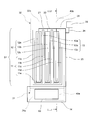
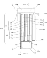
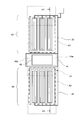
- FIG. 1A is a schematic plan view of a semiconductor device according to a first embodiment of the present invention.
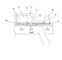
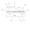
- FIG. 1B is a schematic cross-sectional view of the main part viewed from the line IB-IB of 1A.
- FIG. 1C is a schematic plan view showing dimensions of each part of the semiconductor device.
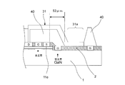
- FIG. 1D is a schematic cross-sectional view showing the dimensions of the main part of the semiconductor device.
- FIG. 1E is a schematic cross-sectional view of the main part viewed from the line IE-IE in FIG. 1A.
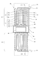
- FIG. 2A is a schematic plan view of a semiconductor device according to a second embodiment of the present invention.
- FIG. 2B is a schematic cross-sectional view of the main part viewed from the line IIB-IIB in FIG.
- FIG. 3A is a schematic plan view of a semiconductor device according to a third embodiment of the present invention.
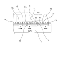
- FIG. 3B is a schematic cross-sectional view of the main part viewed from the line IIIB-IIIB in FIG. 3A.
- FIG. 4A is a schematic plan view of a semiconductor device according to a fourth embodiment of the present invention.
- FIG. 4B is a schematic cross-sectional view of the main part viewed from the line IVB-IVB in FIG. 4A.
- FIG. 5A is a schematic plan view of a semiconductor device according to a fifth embodiment of the present invention.
- FIG. 5B is a schematic cross-sectional view of the main part seen from the line VB-VB in FIG. 5A.
- FIG. 6A is a schematic plan view of a semiconductor device according to a sixth embodiment of the present invention.
- FIG. 6B is a schematic cross-sectional view of the main part viewed from the VIB-VIB line in FIG. 6A.
- FIG. 7A is a schematic plan view of a semiconductor device according to a seventh embodiment of the present invention.
- FIG. 7B is a schematic cross-sectional view of the main part viewed from the line VIIB-VIIB in FIG. 7A.
- FIG. 8 is a schematic plan view of a semiconductor device in which scribe lines are formed.
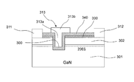
- FIG. 9 is a cross-sectional view of a main part of a recess type semiconductor device.
- FIG. 10 is a cross-sectional view of the main part of another recess type semiconductor device.
- FIG. 9 is a cross-sectional view of a main part of a recess type semiconductor device.
- FIG. 11 is a cross-sectional view of a lateral junction FET.
- FIG. 12 is a cross-sectional view of a lateral power MOSFET.
- FIG. 13 is a cross-sectional view of a conventional horizontal power device.
- FIG. 14A is a schematic plan view of a semiconductor device according to an eighth embodiment of the present invention.
- FIG. 14B is a schematic plan view when the gate electrode is connected between elements.
- FIG. 14C is a schematic cross-sectional view of the main part viewed from the line XIVC-XIVC in FIG. 14A.
- FIG. 15A is a schematic plan view of a semiconductor device according to the ninth embodiment of the present invention.
- FIG. 15B is a schematic plan view when the gate electrode is connected between elements.
- FIG. 15A is a schematic plan view of a semiconductor device according to the ninth embodiment of the present invention.
- FIG. 15B is a schematic plan view when the gate electrode is connected between elements.
- FIG. 15C is a schematic cross-sectional view of the main part viewed from the XVC-XVC line of FIG. 15A.
- FIG. 16A is a schematic plan view of a semiconductor device according to a tenth embodiment of the present invention.
- FIG. 16B is a schematic plan view when the gate electrode is connected between elements.
- FIG. 16C is a schematic cross-sectional view of the main part viewed from the XVIC-XVIC line of FIG. 16A.
- FIG. 17A is a schematic plan view of a semiconductor device according to an eleventh embodiment of the present invention.
- FIG. 17B is a schematic plan view when the gate electrode is connected between elements.
- FIG. 17C is a schematic cross-sectional view of the main part as viewed from line XVIIC-XVIIC in FIG. 17A.
- FIG. 1A is a schematic plan view of a semiconductor device according to a first embodiment of the present invention, which is a GaN-based HFET as an example of the semiconductor device.
- This semiconductor device includes an undoped GaN layer 1 (shown in FIG. 1B) as an example of a first semiconductor layer and an undoped AlGaN layer 2 (see FIG. 1B) as an example of a second semiconductor layer on a Si substrate (not shown).
- 2DEG two-dimensional electron gas
- the substrate is not limited to the Si substrate, and a sapphire substrate or an SiC substrate may be used, a nitride semiconductor layer may be grown on the sapphire substrate or the SiC substrate, or an AlGaN layer is grown on the GaN substrate.
- a nitride semiconductor layer may be grown on a substrate made of a nitride semiconductor.
- FIG. 1A As shown in FIG. 1A, on the AlGaN layer 2 (shown in FIG. 1B), four comb-like source electrode portions 11a to 11d and four comb-like source electrode portions 11a are arranged substantially parallel to each other at a distance from each other. A source electrode 11 having a connecting base portion 11e that connects one end of each of ⁇ 11d is formed. On the AlGaN layer 2, a drain electrode 12 comprising three comb drain electrode portions 12a, 12b and 12c arranged between the comb source electrode portions 11a to 11d is formed.
- gate electrode portions 13a formed on the AlGaN layer 2 so as to surround the comb-shaped drain electrode portions 12a, 12b, and 12c so as to surround the comb-shaped drain electrode portions 12a, 12b, and 12c. , 13b, 13c is formed.
- the region indicated by the alternate long and short dashed line) constitutes the switching element S1.
- the active region A1 is a carrier between the source electrode 11 and the drain electrode 12 by a voltage applied to the gate electrode 13 disposed between the source electrode 11 and the drain electrode 12 on the AlGaN layer 2.
- This is a region of the semiconductor layer (GaN layer 1, AlGaN layer 2) through which.
- connection base portion 11 e of the source electrode 11 is connected to the AlGaN layer 2 via connection wirings 21, 22.
- the source electrode 11 and the drain electrode 12 have a thickness of 550 nm and a width of 4 ⁇ m
- the gate electrode 13 has a thickness of 200 nm and a width of 4.5 ⁇ m.
- an insulating film 30 made of SiN and having a thickness of 200 nm (see FIG. 1B).
- An interlayer insulating film 40 (shown in FIG. 1B) made of polyimide and having a thickness of 9 ⁇ m is formed on a Si substrate (not shown) on which the source electrode 11, the drain electrode 12, and the gate electrode 13 are formed. .
- the insulating film 30 (shown in FIG. 1B) is formed at the bottom of the interlayer insulating film 40 outside the connecting base portion 11e of the source electrode 11 and in the region where the 2GaN is removed by removing a part of the AlGaN layer 2 and the GaN layer 1.
- a drain electrode pad 31 (thickness: 3 ⁇ m) is formed so as to cover the recess 40a where the is exposed and to cover the recess 40a and the region of the source electrode 11 on the connection base 11e side.
- the drain electrode pad 31 overlaps one end of the comb-shaped drain electrode portions 12a, 12b, and 12c, and the drain electrode pad 31 and the comb-shaped drain electrode portions 12a, 12b, and 12c are contact portions (not shown) in the overlapping region. ). Further, the region in contact with the insulating film 30 (shown in FIG. 2B) exposed at the bottom of the recess 40a of the drain electrode pad 31 is interposed on the GaN layer 1 outside the active region A1 where the switching element S1 is formed via the insulating film 30. This is a bondable region 31a formed in the above manner.
- a concave portion 40b in which the insulating film 30 (shown in FIG.
- the source electrode pad 32 (thickness 3 ⁇ m) is formed so as to cover the recess 40b and the region of the source electrode 11 on the side opposite to the connection base portion 11e.
- the source electrode pad 32 overlaps the other ends of the comb-shaped source electrode portions 11a to 11d, and the source electrode pad 32 and the comb-shaped drain electrode portions 12a, 12b, and 12c are contact portions (not shown) in the overlapping region. Connected through.
- a region in contact with the insulating film 30 (shown in FIG. 1B) exposed at the bottom of the recess 40b of the source electrode pad 32 is a bondable region 32a.
- the gate electrode pad 33 is formed on the side of the bondable region 32a of the source electrode pad 32 and on the GaN layer 1 through the insulating film 30 (shown in FIG. 1B). In addition, the gate electrode pad 33 is connected to one end of the gate electrode portion 13 c to which the connection wiring 22 is connected through connection wirings 23 and 24. Further, the gate electrode extending portion 14 is formed between the source electrode 11 and the bondable region 31 a of the drain electrode pad 31 so as to surround the bondable region 31 a. The gate electrode extending portion 14 is connected to the connection point of the connection wirings 23 and 24 through the connection wiring 25.
- Ti / Au, Hf / Al / Hf / Au, etc. are used for the source electrode 11 and the drain electrode 12, and the AlGaN layer 2 and the shot are formed for the gate electrode 13, the gate electrode extending portion 14 and the connection wirings 21 to 25.
- WN or TiN is used as a material for key joining.
- Ti / Au or Ti / Al is used for the drain electrode pad 31, the source electrode pad 32, and the gate electrode pad 33.
- SiO 2 , Al 2 O 3 or the like is used for the insulating film 30.
- SiO 2 , Al 2 O 3 or the like is used for the interlayer insulating film 40.
- SOG Spin On Glass
- BPSG BPSG
- An insulating material such as Phosphor Silicate Glass (boron, phosphorus, silicate, glass) may be used.
- the semiconductor device has one element pattern formed of a source electrode 11, a drain electrode 12, and a gate electrode 13 shown in FIG. 1A on a Si substrate on which a GaN layer 1 and an AlGaN layer 2 are formed. After a plurality of layers are formed, a part of the AlGaN layer 2 and the GaN layer 1 in the region corresponding to the electrode pad portion is removed, and the insulating film 30 and the interlayer insulating film 40 are formed in order, and the drain electrode pad 31 is formed in the removed region. After the source electrode pad 32 and the gate electrode pad 33 are formed, they are divided into a plurality of chips by dicing along a scribe line (not shown).
- FIG. 1B is a schematic cross-sectional view of the main part viewed from the line IB-IB in FIG. 1A, and the Si substrate is omitted in FIG. 1B.
- 2DEG two-dimensional electron gas formed at the interface between the GaN layer 1 and the AlGaN layer 2 is generated to form a channel layer.
- the heterojunction field effect transistor having the source electrode 11, the drain electrode 12, and the gate electrode 13 is turned on and off.
- a depletion layer is formed in the GaN layer 1 below the gate electrode portions 13a, 13b, and 13c (only 13c is shown in FIG. 1B).
- the voltage of the gate electrode 13 is zero, the GaN layer 1 under the gate electrode portions 13a, 13b, and 13c (only 13c is shown in FIG. 1B) has no depletion layer and is normally turned on. It is an on-type transistor.
- FIG. 1C is a schematic plan view showing dimensions of each part of the semiconductor device.
- the same reference numerals as those of the semiconductor device shown in FIG. 1A are attached.
- the horizontal dimension of the drain electrode pad 31 and the source electrode pad 32 in FIG. 1C varies depending on the number of fingers of the source electrode 11 and the drain electrode 12.
- 1D is a schematic cross-sectional view showing the dimensions of the main part of the semiconductor device.
- the distance between the connection base 11e of the source electrode 11 and the bondable region 31a of the drain electrode pad 31 is 53 ⁇ m. It is.
- FIG. 1E is a schematic cross-sectional view of the main part viewed from the line IE-IE in FIG. 1A.
- the thickness of the interlayer insulating film 40 is shown to be thinner than that in FIG. 1B.
- a semiconductor layer 20 composed of an undoped GaN layer 1 and an undoped AlGaN layer 2 (shown in FIG. 1B) is formed on an Si substrate 10.
- drain electrode pad 31 and the three comb-shaped drain electrode portions 12a, 12b, and 12c are connected through the via 45 as the contact portion.
- the drain electrode and the drain electrode pad (and the source electrode and the source electrode pad) may be connected using an opening or the like provided in the insulating film.
- the gate electrode 13 (only the gate electrode portion 13a is shown in FIG. 1E) is formed in a shape so as to have a field plate structure, and has a structure in which the drain side of the gate electrode 13 protrudes on the insulating film 30. Yes.
- a field plate structure By adopting such a field plate structure, there is an effect that the collapse characteristic which is a problem of the GaN HFET can be suppressed.
- the gate electrode extending portion 14 connected to the gate electrode 13 is formed between the source electrode 11 and the bondable region 31a of the drain electrode pad 31 to be applied to the gate electrode 13.
- the depletion layer is formed in the GaN layer 1 below the gate electrode extension 14 between the source electrode 11 and the bondable region 31a of the drain electrode pad 31 by controlling the voltage to be applied, that is, the voltage of the gate electrode extension 14.
- the withstand voltage between the bondable region 31a of the drain electrode pad 31 formed on the insulating film 30 without the interlayer insulating film 40 and the source electrode 11 can be improved without increasing the element size.
- a leakage current between the source electrode 11 and the bondable region 31 a of the drain electrode pad 31 is formed. Can be reliably suppressed.
- the bondable region 31a of the drain electrode pad 31 is formed on the insulating film 30 without the interlayer insulating film 40, the breakdown voltage between the bondable region 31a of the drain electrode pad 31 and the source electrode 11 can be improved, and the element The size can be reduced.
- FIG. 2A is a schematic plan view of a semiconductor device according to the second embodiment of the present invention.
- the semiconductor device of the second embodiment has the same configuration as that of the semiconductor device of the first embodiment except that a part of the semiconductor layer is not removed, and the same reference numerals are given to the same components. A description thereof will be omitted.
- the bondable region 31a of the drain electrode pad 31 is formed on the AlGaN layer 2 without removing the AlGaN layer 2 outside the active region of the transistor.
- a gate electrode extending portion 14 is provided on the AlGaN layer 2 so as to surround the bondable region 31a.
- a negative voltage is also applied to 14 to form a depletion layer.
- FIG. 3A is a schematic plan view of a semiconductor device according to a third embodiment of the present invention.
- the semiconductor device according to the third embodiment has the same configuration as that of the semiconductor device according to the second embodiment except for the connection electrode that connects the bondable region of the drain electrode pad and the semiconductor layer.
- connection electrode that connects the bondable region of the drain electrode pad and the semiconductor layer.
- the semiconductor device according to the third embodiment includes a bondable region 31a and an AlGaN layer in a region in contact with the insulating film 30 (shown in FIG. 3B) exposed at the bottom of the recess 40a of the drain electrode pad 31. 2 is formed along the outer edge of the bondable region 31a.
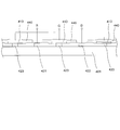
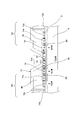
- FIG. 3B is a schematic cross-sectional view of the main part as viewed from line IIIB-IIIB in FIG. 3A.
- FIG. 3B In the off state in which a negative voltage is applied to the gate electrode 13 and a depletion layer is formed in the GaN layer 1, FIG.
- the gate electrode extending portion 14 existing between the bondable region 31a of the pad 31 and the active region of the transistor surrounded by the dotted line causes a gap between the connection base portion 11e of the source electrode 11 and the bondable region 31a of the drain electrode pad 31.
- a depletion layer is formed in the GaN layer 1 region.
- the insulating film 30 on the lower side of the bondable region 31 a of the drain electrode pad 31 is formed. An electric field is not applied, and the dielectric breakdown of the insulating film 30 can be prevented.
- the semiconductor device of the third embodiment has the same effect as the semiconductor device of the second embodiment.
- FIG. 4A is a schematic plan view of a semiconductor device according to the fourth embodiment of the present invention
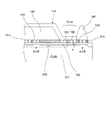
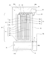
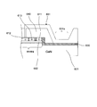
- FIG. 4B is a schematic cross-sectional view of the main part viewed from the line IVB-IVB in FIG. 4A.
- the semiconductor device according to the fourth embodiment has the same configuration as that of the semiconductor device according to the third embodiment except for the element isolation region, and the same reference numerals are given to the same components and the description thereof is omitted.
- the semiconductor device includes a GaN layer 1 between the gate electrode extending portion 14 and the connecting base portion 11e of the source electrode 11 adjacent to the gate electrode extending portion 14, In the region of the AlGaN layer 2, an element isolation region 60 penetrating the AlGaN layer 2 and embedded in a part of the upper side of the GaN layer 1 is formed.
- the element isolation region 60 is made of an insulator and may be a silicon oxide film or a silicon nitride film.
- the semiconductor device according to the fourth embodiment has the same effect as the semiconductor device according to the third embodiment.
- the gate electrode extension portion 14 and the gate electrode extension portion 14 are adjacent to each other.
- the connection base portion 11e of the source electrode 11 and the gate electrode extension portion 14 forming the pseudo transistor are formed. Are separated by the element isolation region 60, so that malfunction of the pseudo transistor can be reliably prevented.
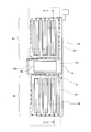
- FIG. 5A is a schematic plan view of a semiconductor device according to a fifth embodiment of the present invention, which is a GaN-based HFET as an example of the semiconductor device.
- This semiconductor device includes an undoped GaN layer 101 (shown in FIG. 5B) as an example of a first semiconductor layer and an undoped AlGaN layer 102 (see FIG. 5B) as an example of a second semiconductor layer on a Si substrate (not shown).
- an undoped GaN layer 101 shown in FIG. 5B
- an undoped AlGaN layer 102 see FIG. 5B
- 2DEG two-dimensional electron gas
- the substrate is not limited to the Si substrate, and a sapphire substrate or an SiC substrate may be used, a nitride semiconductor layer may be grown on the sapphire substrate or the SiC substrate, or an AlGaN layer is grown on the GaN substrate. As described above, a nitride semiconductor layer may be grown on a substrate made of a nitride semiconductor.
- a source electrode 111 having a connecting base 111e is formed.
- the connection base 111e of the source electrode 111 is provided on the side opposite to the connection base 11e of the source electrode 11 of the semiconductor device shown in FIG. 1A of the first embodiment.
- a drain electrode 112 composed of three comb drain electrode portions 112a, 112b and 112c arranged between the comb source electrode portions 111a to 111d is formed.
- three gate electrode portions 113a formed on the AlGaN layer 102 so as to surround the comb drain electrode portions 112a, 112b, and 112c and spaced from the comb drain electrode portions 112a, 112b, and 112c. , 113b, 113c is formed.
- Each of the gate electrode portions 113a, 113b, 113c has end portions a1, a2 on one side of the gate electrode portion 113a (the side opposite to the coupling base portion 111e of the source electrode 111) and one side of the gate electrode portion 113b (source electrode).
- 111 having an end b1, b2 on the side opposite to the connecting base 111e) and an end c1, c2 on one side of the gate electrode 113c (the side opposite to the connecting base 111e of the source electrode 111). I am doing.
- the gate electrodes 113a and 113b are connected at their open ends a2 and b1 adjacent to each other by a gate electrode extending portion 115, and the gate electrodes 113b and 113c are connected at their open ends b2 and c1 as gate electrodes. They are connected by the extending part 116.
- the gate-shaped gate is formed so that the outer end a1 on the open side of the gate electrode portion 113a and the outer end c2 on the open side of the gate electrode portion 113c surround a part of the bondable region 131a.
- the electrodes are connected by the electrode extending portion 114.
- the source electrode 111 and the drain electrode 112 have a thickness of 550 nm and a width of 4 ⁇ m
- the gate electrode 113 has a thickness of 200 nm and a width of 4.5 ⁇ m.
- a 200 nm thick insulating film 130 (shown in FIG. 5B) is formed. Further, an interlayer insulating film 140 (shown in FIG. 5B) made of polyimide and having a thickness of 9 ⁇ m is formed on a Si substrate (not shown) on which the source electrode 111, the drain electrode 112, and the gate electrode 113 are formed. .
- a recess 140a in which the insulating film 130 (shown in FIG. 5B) is exposed at the bottom is formed outside the gate electrode extending portions 115 and 116 with respect to the source electrode 111 and the drain electrode 112 of the interlayer insulating film 140.
- a drain electrode pad 131 (thickness 3 ⁇ m) is formed so as to cover a region on the opposite side of the connection base 111e of the source electrode 111 in the vicinity of 140a and the recess 140a.
- the drain electrode pad 131 overlaps one end of the comb-shaped drain electrode portions 112a, 112b, and 112c on the side opposite to the connection base portion 111e of the source electrode 111, and the drain electrode pad 131 and the comb-shaped drain electrode portion 112a overlap in the overlapping region.
- 112b and 112c are connected to each other through a contact portion (not shown).
- a region in contact with the insulating film 130 (shown in FIG. 5B) exposed at the bottom of the recess 140a of the drain electrode pad 131 is a bondable region 131a.
- a recess 140b in which the insulating film 130 (shown in FIG. 5B) is exposed is formed at the bottom, and the recess 140b and A source electrode pad 132 (thickness 3 ⁇ m) is formed so as to cover the region of the source electrode 111 on the connection base 111e side.
- the source electrode pad 132 overlaps one end of the comb-shaped source electrode portions 111a to 111d on the coupling base 111e side, and the source electrode pad 132 and the comb-shaped source electrode portions 111a to 111d are contact portions (not shown) in the overlapping region. )).
- a region in contact with the insulating film 130 (shown in FIG. 5B) exposed at the bottom of the recess 140b of the source electrode pad 132 is a bondable region 132a.
- the gate electrode pad 133 is formed on the AlGaN layer 102 and on the side of the bondable region 132a of the source electrode pad 132 through an insulating film 130 (shown in FIG. 5B).
- the gate electrode pad 133 is connected to one end c2 of the gate electrode portion 113c via a connection wiring 121.
- Ti / Au, Hf / Al / Hf / Au, etc. are used for the source electrode 111 and the drain electrode 112, and the AlGaN layer 102 and the Schottky junction are used for the gate electrode 113 and the gate electrode extending portions 114, 115, 116.
- WN / W or TiN / Ti is used as the material to be formed.
- Ti / Au or Ti / Al is used for the drain electrode pad 131, the source electrode pad 132, and the gate electrode pad 133.
- SiO 2 , Al 2 O 3 or the like may be used for the insulating film 130, and an insulating material such as SOG or BPSG may be used for the interlayer insulating film 140 in addition to polyimide.
- a plurality of one element patterns of the source electrode 111, the drain electrode 112, and the gate electrode 113 shown in FIG. 5A are formed on the Si substrate on which the GaN layer 101 and the AlGaN layer 102 are formed. Then, an insulating film 130 and an interlayer insulating film 140 are formed in order, and further, a drain electrode pad 131, a source electrode pad 132, and a gate electrode pad 133 corresponding to each element pattern are formed, and then along a scribe line (not shown). Then, it is divided into a plurality of chips by dicing.
- FIG. 5B shows a schematic cross-sectional view of the main part seen from the line VB-VB in FIG. 5A, and the Si substrate is omitted in FIG. 5B.
- 2DEG two-dimensional electron gas formed at the interface between the GaN layer 101 and the AlGaN layer 102 is generated to form a channel layer.
- the heterojunction field effect transistor including the source electrode 111, the drain electrode 112, and the gate electrode 113 is turned on and off.
- the gate electrode portions 113a, 113b, 113c and the gate electrode extending portions 114, 115, 116 are shown in FIG. 5B).
- a depletion layer is formed in the lower GaN layer 101 to be turned off, while the GaN layer under the gate electrode portions 13a, 13b, 13c and the gate electrode extension portions 114, 115, 116 when the voltage of the gate electrode 13 is zero 101 is a normally-on type transistor in which a depletion layer disappears and is turned on.
- gate electrode extension portions 115 which exist between the bondable region 131a of the drain electrode pad 131 and the active region of the transistor, 116 (only 116 is shown in FIG. 5B)
- a depletion layer is formed in the region of the GaN layer 101 between the comb-like source electrode portion 111c of the source electrode 111 and the bondable region 131a of the drain electrode pad 131. This effectively suppresses the leakage current between the comb-like source electrode portion 111c of the source electrode 111 and the bondable region 131a of the drain electrode pad 131, thereby improving the breakdown voltage.
- the semiconductor device of the fifth embodiment has the same effect as the semiconductor device of the first embodiment.
- FIG. 6A is a schematic plan view of a semiconductor device according to a sixth embodiment of the present invention.
- the semiconductor device according to the sixth embodiment has the same configuration as that of the semiconductor device according to the fifth embodiment except for the connection electrode that connects the bondable region of the drain electrode pad and the semiconductor layer.
- connection electrode that connects the bondable region of the drain electrode pad and the semiconductor layer.
- a bondable region 131a and an AlGaN layer are formed in a region in contact with the insulating film 130 (shown in FIG. 6B) exposed at the bottom of the recess 140a of the drain electrode pad 131.
- a connection electrode 150 is formed along the outer edge of the bondable region 131a.
- FIG. 6B is a schematic cross-sectional view of the main part viewed from the line VIB-VIB in FIG. 6A.
- FIG. Gate electrode extension portions 115 and 116 (only 116 is shown in FIG. 6B) existing between the bondable region 131a of the pad 131 and the active region of the transistor, and the source electrode portion 111c of the source electrode 111 and the drain electrode pad.
- a depletion layer is formed in the region of the GaN layer 101 between the bondable region 131a of 131.
- the connection electrode 150 penetrating the insulating film 130, the insulating film 130 below the bondable region 131a of the drain electrode pad 131 is formed. An electric field is not applied, and the dielectric breakdown of the insulating film 130 can be prevented.
- the semiconductor device according to the sixth embodiment has the same effect as the semiconductor device according to the first embodiment.
- FIG. 7A is a schematic plan view of a semiconductor device according to a seventh embodiment of the present invention.
- the semiconductor device of the seventh embodiment has the same configuration as that of the semiconductor device of the sixth embodiment except for the element isolation region, and the same reference numerals are given to the same components, and the description thereof is omitted.
- FIG. 7B is a schematic cross-sectional view of the main part viewed from the line VIIB-VIIB in FIG. 7A.
- the semiconductor device according to the seventh embodiment includes a gate electrode extension 114 and its gate electrode as shown in FIG. 7B.
- an element isolation region 160 that penetrates the AlGaN layer 102 and is embedded in a part on the upper side of the GaN layer 101. Is forming.
- the element isolation region 160 is made of an insulator and may be a silicon oxide film or a silicon nitride film.
- the semiconductor device of the third embodiment has the same effect as the semiconductor device of the second embodiment.
- FIG. 8 is a schematic plan view of a semiconductor device in which a scribe line 70 surrounding one element pattern formed by the electrode 12 and the gate electrode 13 is further formed.
- the source electrode can be applied to the drain electrode under the condition of 0V and the gate electrode of ⁇ 10V.
- the maximum voltage was 700V.
- the maximum voltage that can be applied to the drain electrode is 900 V
- the maximum voltage that can be applied to the drain electrode is 1200 V.
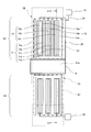
- FIG. 14A and 14B are schematic plan views of the semiconductor device according to the eighth embodiment of the present invention.
- the semiconductor device of the eighth embodiment two switching elements S1 and S2 having the same configuration as those of the semiconductor device of the second embodiment are connected by the drain electrode pad 31, and the same reference numerals are assigned to the same components. A description thereof will be omitted.
- the semiconductor device in FIG. 14A is a configuration example in which the gate electrode pad 33 of the lower switching element S2 is not connected to the gate electrode extending portion 14, and the semiconductor device in FIG. 14B has the lower switching element S2.
- the gate electrode 13 is connected to the gate electrode extending portion 14 via the connection wiring 25 without providing the gate electrode pad on the side.
- FIG. 14C is a schematic cross-sectional view of the main part viewed from the XIVC-XIVC line in FIGS. 14A and 14B.
- the drain electrode pad 31 is provided on the AlGaN layer 2 without removing the AlGaN layer 2 outside the active regions A1 and A2 of the switching elements S1 and S2. Further, the gate electrode extending portion 14 is provided on the AlGaN layer 2 so as to surround a region where the drain electrode pad 31 is in contact with the AlGaN layer 2.
- the drain electrode pad 31 is in contact with the AlGaN layer and the active region A1 of the transistor in the off state in which a negative voltage is applied to the gate electrode 13 and the depletion layer is formed in the GaN layer 1.
- A2 is also applied to the gate electrode extending portion 14 formed between the two and A2, and a depletion layer is formed.
- the leakage current between the connection base portion 11e of the source electrode 11 and the region where the drain electrode pad 31 is in contact with the AlGaN layer 2 can be effectively suppressed.
- 2DEG may exist under the drain electrode pad 31.
- the semiconductor device of the eighth embodiment has the same effect as the semiconductor device of the second embodiment.
- the element size can be reduced.
- drain electrode pad 31 does not necessarily have to be bonded, and depending on the circuit, it may not be bonded.
- the semiconductor device having two switching elements has been described.
- the present invention may be applied to a semiconductor device having three or more switching elements.
- FIGS. 15A and 15B are schematic plan views of the semiconductor device according to the ninth embodiment of the present invention.
- the semiconductor device according to the ninth embodiment has the same configuration as that of the semiconductor device according to the eighth embodiment except for the connection electrode 50, and the same reference numerals are given to the same components and description thereof is omitted.
- the semiconductor device of FIG. 15A is a configuration example in which the gate electrode pad 33 of the lower switching element S2 is not connected to the gate electrode extending portion 14, and the semiconductor device of FIG. In this configuration example, the gate electrode 13 is connected to the gate electrode extending portion 14 via the connection wiring 25 without providing the gate electrode pad on the side.
- a bondable region 31a is formed in a region in contact with the insulating film 30 (shown in FIG. 15C) exposed at the bottom of the recess 40a of the drain electrode pad 31.
- the AlGaN layer 2 are formed along the outer edge of the bondable region 31a.
- FIG. 15C is a schematic cross-sectional view of the main part seen from the XVC-XVC line in FIGS. 15A and 15B.
- a depletion layer is formed in the GaN layer 1.
- the connection base 11e of the source electrode 11 and the drain electrode pad 31 are bonded by the gate electrode extending portion 14 existing between the bondable region 31a of the drain electrode pad 31 and the active regions A1 and A2 of the transistor surrounded by the dotted line.
- a depletion layer is formed in the region of the GaN layer 1 between the possible region 31a.
- the insulating film 30 on the lower side of the bondable region 31 a of the drain electrode pad 31 is formed. An electric field is not applied, and the dielectric breakdown of the insulating film 30 can be prevented.
- the semiconductor device of the ninth embodiment has the same effect as the semiconductor device of the eighth embodiment.
- [Tenth embodiment] 16A and 16B are schematic plan views of the semiconductor device according to the tenth embodiment of the present invention.
- the semiconductor device according to the tenth embodiment has the same configuration as that of the semiconductor device according to the ninth embodiment except for the element isolation region 60, and the same reference numerals are given to the same components and the description thereof is omitted. .
- the semiconductor device of FIG. 16A is a configuration example in which the gate electrode pad 33 of the lower switching element S2 is not connected to the gate electrode extending portion 14, and the semiconductor device of FIG. In this configuration example, the gate electrode 13 is connected to the gate electrode extending portion 14 via the connection wiring 25 without providing the gate electrode pad on the side.
- the GaN between the gate electrode extending portion 14 and the connecting base portion 11e of the source electrode 11 adjacent to the gate electrode extending portion 14 is provided.
- an element isolation region 60 penetrating the AlGaN layer 2 and embedded in a part on the upper side of the GaN layer 1 is formed.
- the element isolation region 60 is made of an insulator and may be a silicon oxide film or a silicon nitride film.
- the semiconductor device of the tenth embodiment has the same effect as the semiconductor device of the ninth embodiment.
- the gate electrode extension portion 14 and the gate electrode extension portion 14 are adjacent to each other.
- the connection base portion 11e of the source electrode 11 and the gate electrode extension portion 14 forming the pseudo transistor are formed. Are separated by the element isolation region 60, so that malfunction of the pseudo transistor can be reliably prevented.
- FIGS. 17A and 17B are schematic plan views of the semiconductor device according to the eleventh embodiment of the present invention.
- the semiconductor device according to the eleventh embodiment has the same configuration as that of the semiconductor device according to the ninth embodiment except that a part of the semiconductor layer is removed. A description thereof will be omitted.
- the semiconductor device of FIG. 17A is a configuration example in which the gate electrode pad 33 of the lower switching element S2 is not connected to the gate electrode extending portion 14, and the semiconductor device of FIG. In this configuration example, the gate electrode 13 is connected to the gate electrode extending portion 14 via the connection wiring 25 without providing the gate electrode pad on the side.
- An insulating film 30 (shown in FIG. 17C) at the bottom of the interlayer insulating film 40 outside the connecting base portion 11e of the source electrode 11 is removed from the AlGaN layer 2 and a part of the GaN layer 1 to remove 2DEG.
- the drain electrode pad 31 is formed so as to cover the recessed portion 40a where is exposed and to cover the recessed portion 40a and the region of the source electrode 11 on the connection base portion 11e side.
- the semiconductor device of the eleventh embodiment has the same effect as the semiconductor device of the ninth embodiment.
- the probability of dielectric breakdown in the withstand voltage test between 2DEG (two-dimensional electron gas) and the electrode pad on the insulating film is the gate electrode extending portions 14, 114 to 116 and the connection electrodes 50,
- the number of semiconductor devices having no 150 was significantly reduced to 0% compared to about 40%.
- the heterojunction field effect transistor in which the GaN layers 1 and 101 and the AlGaN layers 2 and 102 are sequentially stacked on the substrate has been described.
- a GaAs layer is used instead of the GaN layer and the AlGaN layer.
- the present invention may be applied to a heterojunction field effect transistor in which an n-AlGaAs layer is sequentially laminated on a substrate.
- the finger type heterojunction field effect transistor having a plurality of gate electrodes, source electrodes, and drain electrodes has been described.
- the semiconductor device of the present invention is not limited to this, and the gate electrode The present invention may be applied to a semiconductor device including a switching element having a pair of a source electrode and a drain electrode.
- the normally-on type heterojunction field effect transistor has been described.
- the semiconductor device of the present invention is not limited to this, and the normally-off type heterojunction field effect transistor is not limited to this.
- the invention may be applied.
- FIG. 9 shows a cross-sectional view of the main part of a recess type semiconductor device, which is a GaN-based HFET as an example of the semiconductor device.
- a recess type semiconductor device which is a GaN-based HFET as an example of the semiconductor device.
- interlayer insulating films and electrode pads are omitted.
- an undoped GaN layer 201 as an example of a first semiconductor layer and an undoped AlGaN layer 202 as an example of a second semiconductor layer are sequentially formed on a Si substrate (not shown).
- 2DEG two-dimensional electron gas
- the substrate is not limited to the Si substrate, and a sapphire substrate or SiC substrate may be used, and a nitride semiconductor layer may be grown on the sapphire substrate or SiC substrate.
- a nitride semiconductor layer may be grown on a substrate made of a nitride semiconductor, such as by growing an AlGaN layer on a GaN substrate.
- a source electrode 211 and a drain electrode 212 are formed on the AlGaN layer 202 with a predetermined interval.
- a recess 200 is provided in the upper part of the AlGaN layer 202.
- a first insulating film 230 is formed on the AlGaN layer 202 excluding the recess 200, the source electrode 211, and the drain electrode 212.
- a second insulating film 240 is formed so as to cover the first insulating film 230 and the recess 200.
- a gate electrode 213 is formed by a base portion 213a embedded in the concave portion 200 covered with the second insulating film 240 and a field plate portion 213b formed on the base portion 213a.
- the base 213a of the gate electrode 213 is embedded in the recess 200 formed in a part of the upper side of the AlGaN layer 202, and the AlGaN layer 202 is interposed between the gate electrode 213 and the first insulating film 230.
- 2DEG two-dimensional electron gas
- FIG. 10 shows a cross-sectional view of the main part of another recess type semiconductor device, which is a GaN HFET as an example of the semiconductor device.
- interlayer insulating films and electrode pads are omitted.
- an undoped GaN layer 201 as an example of a first semiconductor layer and an undoped AlGaN layer 302 as an example of a second semiconductor layer are sequentially formed on a Si substrate (not shown).
- 2DEG two-dimensional electron gas
- a source electrode 311 and a drain electrode 312 are formed on the AlGaN layer 302 with a predetermined interval.
- a recess 300 is provided in a part of the upper side of the GaN layer 301 through the AlGaN layer 302.
- a first insulating film 330 is formed on the AlGaN layer 302 excluding the recess 300, the source electrode 311, and the drain electrode 312.
- a second insulating film 340 is formed so as to cover the first insulating film 330 and the recess 300.
- a gate electrode 313 is formed by a base portion 313a embedded in the recess 300 covered with the second insulating film 340 and a field plate portion 313b formed on the base portion 313a.
- the base 313 a of the gate electrode 313 is embedded in the recess 300 formed in the upper part of the GaN layer 301 through the AlGaN layer 302, so that the GaN layer is formed by the gate electrode 313. Since the hetero interface between the 301 and the AlGaN layer 302 is cut off, 2DEG (two-dimensional electron gas) does not exist and the threshold voltage becomes high, the switching element can be normally off.
- 2DEG two-dimensional electron gas
- the gate electrode extending portion connected to the gate electrode of the switching element is formed on the semiconductor layer and at least a bondable region between the source electrode and the drain electrode pad.
- the present invention can be applied by forming between the two. As a result, a normally-off type heterojunction field effect that can improve the breakdown voltage between the bondable region of the drain electrode pad formed on the insulating film without the interlayer insulating film and the source electrode without increasing the element size.
- a transistor can be realized.
- the semiconductor device according to the present invention is not limited to a heterojunction field effect transistor, and is not limited to a semiconductor device in which carriers such as a lateral junction FET shown in FIG. 11 and a lateral power MOSFET shown in FIG. 12 move laterally along the substrate surface.
- the invention may be applied.
- FIG. 11 showing a general configuration of a lateral junction FET
- 401 is an n-type semiconductor substrate
- 413 is a gate electrode
- 421 is a source region
- 422 is a drain region
- 423 is a gate layer
- 430 is an insulating film
- 440 is an oxide film. It is.
- FIG. 12 which shows a general configuration of a lateral power MOSFET
- 501 is a p-type semiconductor substrate
- 511 is a source electrode
- 512 is a drain electrode
- 513 is a gate electrode
- 521 is a source region
- 522 is a drain region
- 530 is It is an insulating film.
- the gate electrode extending portion connected to the gate electrode of the switching element is bonded to the semiconductor layer and at least the source electrode and drain electrode pad of the switching element.
- the present invention can be applied by forming between the possible regions. This realizes a lateral junction FET and a lateral power MOSFET that can improve the breakdown voltage between the bondable region of the drain electrode pad formed on the insulating film without the interlayer insulating film and the source electrode without increasing the element size. can do.
- Insulating film 440 Oxide film 501 ... P-type semiconductor substrate 511 ... Source electrode 512 ... Drain electrode 513 ... Gate electrode 521 ... Source region 522 ... Drain region 530 ... Insulating film A1, A2 ... Active region S1, S2, S101 ... Switching element
Landscapes
- Junction Field-Effect Transistors (AREA)
- Electrodes Of Semiconductors (AREA)
- Insulated Gate Type Field-Effect Transistor (AREA)
Abstract
Description
基板と、
上記基板上に形成されると共に、活性領域を含む半導体層と、
上記半導体層の上記活性領域上に形成されたゲート電極とソース電極とドレイン電極とを有するスイッチング素子と、
上記ドレイン電極に接続され、上記半導体層の上記活性領域以外の領域上に絶縁膜を介して形成されたボンディング可能領域を有するドレイン電極パッドと、
上記半導体層上、かつ、少なくとも上記ソース電極と上記ドレイン電極パッドのボンディング可能領域との間に形成され、上記ゲート電極に接続されたゲート電極延伸部と
を備えたことを特徴とする。
ここで、活性領域とは、半導体層上のソース電極とドレイン電極との間に配置されたゲート電極に印加される電圧によって、ソース電極とドレイン電極との間でキャリアが流れる半導体層の領域である。
上記半導体層は、上記基板上に順に積層された第1半導体層およびその第1半導体層とヘテロ界面を形成する第2半導体層を含み、
上記スイッチング素子は、上記第1半導体層と上記第2半導体層とのヘテロ界面に形成された2次元電子ガスを利用するヘテロ接合電界効果トランジスタである。
上記2次元電子ガスが形成される上記第1半導体層と上記第2半導体層とのヘテロ界面は、上記ドレイン電極パッドのボンディング可能領域の下側の領域を少なくとも除く上記基板上の領域に形成されている。
上記第2半導体層の上側の一部、または、上記第2半導体層を貫通して上記第1半導体層の上側の一部に凹部が形成され、
上記凹部に上記ゲート電極の少なくとも一部が埋め込まれている。
上記ドレイン電極パッドのボンディング可能領域の下側かつ少なくとも上記ゲート電極延伸部に対向する領域に形成され、上記絶縁膜を貫通して上記ドレイン電極パッドのボンディング可能領域と上記半導体層とを接続する接続電極を備えた。
上記ゲート電極延伸部とそのゲート電極延伸部に隣接する上記ソース電極との間の上記半導体層の領域に形成された素子分離領域を備えた。
上記ゲート電極延伸部は、上記ドレイン電極パッドのボンディング可能領域を囲むように上記半導体層上に形成されている。
上記ソース電極は、互いに間隔をあけて略平行に配列された複数のくし状ソース電極部を有すると共に、
上記ドレイン電極は、上記ソース電極の複数のくし状ソース電極部と互いに間隔をあけて交互に配列された複数のくし状ドレイン電極部を有する。
上記スイッチング素子は複数であって、
上記複数のスイッチング素子の上記ドレイン電極は、同一の上記ドレイン電極パッドを介して接続されている。
図1Aはこの発明の第1実施形態の半導体装置の平面模式図を示しており、半導体装置の一例としてのGaN系HFETである。
ここで、活性領域A1とは、AlGaN層2上のソース電極11とドレイン電極12との間に配置されたゲート電極13に印加される電圧によって、ソース電極11とドレイン電極12との間でキャリアが流れる半導体層(GaN層1,AlGaN層2)の領域である。
図2Aはこの発明の第2実施形態の半導体装置の平面模式図を示している。この第2実施形態の半導体装置は、半導体層の一部を除去していない点を除いて第1実施形態の半導体装置と同一の構成をしており、同一の構成部には同一参照番号を付して説明を省略する。
図3Aはこの発明の第3実施形態の半導体装置の平面模式図を示している。この第3実施形態の半導体装置は、ドレイン電極パッドのボンディング可能領域と半導体層とを接続する接続電極を除いて第2実施形態の半導体装置と同一の構成をしており、同一の構成部には同一参照番号を付して説明を省略する。
図4Aはこの発明の第4実施形態の半導体装置の平面模式図を示しており、図4Bは図4AのIVB-IVB線から見た要部の断面模式図を示している。この第4実施形態の半導体装置は、素子分離領域を除いて第3実施形態の半導体装置と同一の構成をしており、同一の構成部には同一参照番号を付して説明を省略する。
図5Aはこの発明の第5実施形態の半導体装置の平面模式図を示しており、半導体装置の一例としてのGaN系HFETである。
図6Aはこの発明の第6実施形態の半導体装置の平面模式図を示している。この第6実施形態の半導体装置は、ドレイン電極パッドのボンディング可能領域と半導体層とを接続する接続電極を除いて第5実施形態の半導体装置と同一の構成をしており、同一の構成部には同一参照番号を付して説明を省略する。
図7Aはこの発明の第7実施形態の半導体装置の平面模式図を示している。この第7実施形態の半導体装置は、素子分離領域を除いて第6実施形態の半導体装置と同一の構成をしており、同一の構成部には同一参照番号を付して説明を省略する。
図14A,図14Bはこの発明の第8実施形態の半導体装置の平面模式図を示している。この第8実施形態の半導体装置は、第2実施形態の半導体装置と同一の構成の2つのスイッチング素子S1,S2をドレイン電極パッド31で接続しており、同一の構成部には同一参照番号を付して説明を省略する。
図15A,図15Bはこの発明の第9実施形態の半導体装置の平面模式図を示している。この第9実施形態の半導体装置は、接続電極50を除いて第8実施形態の半導体装置と同一の構成をしており、同一の構成部には同一参照番号を付して説明を省略する。
図16A,図16Bはこの発明の第10実施形態の半導体装置の平面模式図を示している。この第10実施形態の半導体装置は、素子分離領域60を除いて第9実施形態の半導体装置と同一の構成をしており、同一の構成部には同一参照番号を付して説明を省略する。
図17A,図17Bはこの発明の第11実施形態の半導体装置の平面模式図を示している。この第11実施形態の半導体装置は、半導体層の一部を除去している点を除いて第9実施形態の半導体装置と同一の構成をしており、同一の構成部には同一参照番号を付して説明を省略する。
2,102…AlGaN層
11,111…ソース電極
11a~11d,111a~111d…くし状ソース電極部
11e,111e…連結基部
12,112…ドレイン電極
12a,12b,12c,112a,112b,112c…くし状ドレイン電極部
13,113…ゲート電極
13a,13b,13c,113a,113b,113c…ゲート電極部
14,114,115,116…ゲート電極延伸部
21~25,121…接続配線
30,130…絶縁膜
31,131…ドレイン電極パッド
31a,131a…ボンディング可能領域
32,132…ソース電極パッド
32a,132a…ボンディング可能領域
33,133…ゲート電極パッド
40,140…層間絶縁膜
40a,40b,140a,140b…凹部
45…ビア
50,150…接続電極
60,160…素子分離領域
200,300…凹部
201,301…GaN層
202,302…AlGaN層
211,311…ソース電極
212,312…ドレイン電極
213,313…ゲート電極
213a,313a…基部
213b,313b…フィールドプレート部
401…n型半導体基板
413…ゲート電極
421…ソース領域
422…ドレイン領域
423…ゲート層
430…絶縁膜
440…酸化膜
501…p型半導体基板
511…ソース電極
512…ドレイン電極
513…ゲート電極
521…ソース領域
522…ドレイン領域
530…絶縁膜
A1,A2…活性領域
S1,S2,S101…スイッチング素子
Claims (9)
- 基板と、
上記基板上に形成されると共に、活性領域を含む半導体層(1,2,101,102)と、
上記半導体層(1,2,101,102)の上記活性領域上に形成されたゲート電極(13,113)とソース電極(11,111)とドレイン電極(12,112)とを有するスイッチング素子(S1,S2,S101)と、
上記ドレイン電極(12,112)に接続され、上記半導体層(1,2,101,102)の上記活性領域以外の領域上に絶縁膜(30,130)を介して形成されたボンディング可能領域を有するドレイン電極パッド(31,131)と、
上記半導体層(1,2,101,102)上、かつ、少なくとも上記ソース電極(11,111)と上記ドレイン電極パッド(31,131)のボンディング可能領域との間に形成され、上記ゲート電極(13,113)に接続されたゲート電極延伸部(14,114,115,116)と
を備えたことを特徴とする半導体装置。 - 請求項1に記載の半導体装置において、
上記半導体層(1,2,101,102)は、上記基板上に順に積層された第1半導体層(1,101)およびその第1半導体層(1,101)とヘテロ界面を形成する第2半導体層(2,102)を含み、
上記スイッチング素子(S1,S2,S101)は、上記第1半導体層(1,101)と上記第2半導体層(2,102)とのヘテロ界面に形成された2次元電子ガスを利用するヘテロ接合電界効果トランジスタであることを特徴とする半導体装置。 - 請求項2に記載の半導体装置において、
上記2次元電子ガスが形成される上記第1半導体層(1,101)と上記第2半導体層(2,102)とのヘテロ界面は、上記ドレイン電極パッド(31,131)のボンディング可能領域の下側の領域を少なくとも除く上記基板上の領域に形成されていることを特徴とする半導体装置。 - 請求項2または3に記載の半導体装置において、
上記第2半導体層(2,102)の上側の一部、または、上記第2半導体層(2,102)を貫通して上記第1半導体層(1,101)の上側の一部に凹部(200,300)が形成され、
上記凹部(200,300)に上記ゲート電極(13,113)の少なくとも一部が埋め込まれていることを特徴とする半導体装置。 - 請求項1から4までのいずれか1つに記載の半導体装置において、
上記ドレイン電極パッド(31,131)のボンディング可能領域の下側かつ少なくとも上記ゲート電極延伸部(14,114,115,116)に対向する領域に形成され、上記絶縁膜(30,130)を貫通して上記ドレイン電極パッド(31,131)のボンディング可能領域と上記半導体層(1,2,101,102)とを接続する接続電極(50,150)を備えたことを特徴とする半導体装置。 - 請求項5に記載の半導体装置において、
上記ゲート電極延伸部(14,114,115,116)とそのゲート電極延伸部(14,114,115,116)に隣接する上記ソース電極(11,111)との間の上記半導体層(1,2,101,102)の領域に形成された素子分離領域(60,160)を備えたことを特徴とする半導体装置。 - 請求項1から6までのいずれか1つに記載の半導体装置において、
上記ゲート電極延伸部(14,114,115,116)は、上記ドレイン電極パッド(31,131)のボンディング可能領域を囲むように上記半導体層(1,2,101,102)上に形成されていることを特徴とする半導体装置。 - 請求項1から7までのいずれか1つに記載の半導体装置において、
上記ソース電極(11,111)は、互いに間隔をあけて略平行に配列された複数のくし状ソース電極部(11a~11d,111a~111d)を有すると共に、
上記ドレイン電極(12,112)は、上記ソース電極(11,111)の複数のくし状ソース電極部(11a~11d,111a~111d)と互いに間隔をあけて交互に配列された複数のくし状ドレイン電極部(12a,12b,12c,112a,112b,112c)を有することを特徴とする半導体装置。 - 請求項1から8までのいずれか1つに記載の半導体装置において、
上記スイッチング素子(S1,S2)は複数であって、
上記複数のスイッチング素子(S1,S2)の上記ドレイン電極(12)は、同一の上記ドレイン電極パッド(31)を介して接続されていることを特徴とする半導体装置。
Priority Applications (2)
| Application Number | Priority Date | Filing Date | Title |
|---|---|---|---|
| JP2012557863A JP5712231B2 (ja) | 2011-02-15 | 2012-01-24 | 半導体装置 |
| CN201280008771.4A CN103370777B (zh) | 2011-02-15 | 2012-01-24 | 半导体装置 |
Applications Claiming Priority (2)
| Application Number | Priority Date | Filing Date | Title |
|---|---|---|---|
| JP2011030044 | 2011-02-15 | ||
| JP2011-030044 | 2011-02-15 |
Publications (1)
| Publication Number | Publication Date |
|---|---|
| WO2012111393A1 true WO2012111393A1 (ja) | 2012-08-23 |
Family
ID=46672331
Family Applications (1)
| Application Number | Title | Priority Date | Filing Date |
|---|---|---|---|
| PCT/JP2012/051422 Ceased WO2012111393A1 (ja) | 2011-02-15 | 2012-01-24 | 半導体装置 |
Country Status (3)
| Country | Link |
|---|---|
| JP (1) | JP5712231B2 (ja) |
| CN (1) | CN103370777B (ja) |
| WO (1) | WO2012111393A1 (ja) |
Cited By (10)
| Publication number | Priority date | Publication date | Assignee | Title |
|---|---|---|---|---|
| JP2014187059A (ja) * | 2013-03-21 | 2014-10-02 | Toshiba Corp | 半導体装置 |
| JP2015090966A (ja) * | 2013-11-07 | 2015-05-11 | シャープ株式会社 | GaN系電界効果トランジスタおよび窒化物半導体装置 |
| CN105229792A (zh) * | 2013-05-03 | 2016-01-06 | 德克萨斯仪器股份有限公司 | Iii族氮化物晶体管布局 |
| JP2016063167A (ja) * | 2014-09-19 | 2016-04-25 | 株式会社東芝 | 半導体装置 |
| JPWO2016042861A1 (ja) * | 2014-09-17 | 2017-05-25 | シャープ株式会社 | 化合物半導体電界効果トランジスタ |
| JP2017105209A (ja) * | 2017-03-07 | 2017-06-15 | 株式会社小森コーポレーション | グラビアオフセット印刷機 |
| JP2021089934A (ja) * | 2019-12-03 | 2021-06-10 | 株式会社東芝 | 半導体装置 |
| WO2021200566A1 (ja) * | 2020-03-31 | 2021-10-07 | 豊田合成株式会社 | 半導体素子および装置 |
| JP2021163890A (ja) * | 2020-03-31 | 2021-10-11 | 豊田合成株式会社 | 半導体素子および装置 |
| WO2024084652A1 (ja) * | 2022-10-20 | 2024-04-25 | 日本電信電話株式会社 | 電界効果型トランジスタ |
Families Citing this family (4)
| Publication number | Priority date | Publication date | Assignee | Title |
|---|---|---|---|---|
| JP2016021530A (ja) * | 2014-07-15 | 2016-02-04 | ルネサスエレクトロニクス株式会社 | 半導体装置 |
| JP6658441B2 (ja) * | 2016-10-06 | 2020-03-04 | 三菱電機株式会社 | 半導体装置 |
| JP6769400B2 (ja) * | 2017-06-26 | 2020-10-14 | 株式会社デンソー | 半導体装置 |
| DE112019001917T5 (de) * | 2018-04-11 | 2020-12-24 | Rohm Co., Ltd. | Halbleiterbauteil |
Citations (4)
| Publication number | Priority date | Publication date | Assignee | Title |
|---|---|---|---|---|
| JP2005353992A (ja) * | 2004-06-14 | 2005-12-22 | Sanyo Electric Co Ltd | 化合物半導体装置およびその製造方法 |
| JP2007305954A (ja) * | 2006-03-27 | 2007-11-22 | Nichia Chem Ind Ltd | 電界効果トランジスタ及びその装置 |
| JP2010182924A (ja) * | 2009-02-06 | 2010-08-19 | Furukawa Electric Co Ltd:The | トランジスタおよびその製造方法 |
| JP2011023385A (ja) * | 2009-07-13 | 2011-02-03 | Mitsubishi Electric Corp | 半導体装置 |
-
2012
- 2012-01-24 WO PCT/JP2012/051422 patent/WO2012111393A1/ja not_active Ceased
- 2012-01-24 JP JP2012557863A patent/JP5712231B2/ja active Active
- 2012-01-24 CN CN201280008771.4A patent/CN103370777B/zh active Active
Patent Citations (4)
| Publication number | Priority date | Publication date | Assignee | Title |
|---|---|---|---|---|
| JP2005353992A (ja) * | 2004-06-14 | 2005-12-22 | Sanyo Electric Co Ltd | 化合物半導体装置およびその製造方法 |
| JP2007305954A (ja) * | 2006-03-27 | 2007-11-22 | Nichia Chem Ind Ltd | 電界効果トランジスタ及びその装置 |
| JP2010182924A (ja) * | 2009-02-06 | 2010-08-19 | Furukawa Electric Co Ltd:The | トランジスタおよびその製造方法 |
| JP2011023385A (ja) * | 2009-07-13 | 2011-02-03 | Mitsubishi Electric Corp | 半導体装置 |
Cited By (13)
| Publication number | Priority date | Publication date | Assignee | Title |
|---|---|---|---|---|
| JP2014187059A (ja) * | 2013-03-21 | 2014-10-02 | Toshiba Corp | 半導体装置 |
| CN105229792B (zh) * | 2013-05-03 | 2019-10-08 | 德克萨斯仪器股份有限公司 | Iii族氮化物晶体管布局 |
| CN105229792A (zh) * | 2013-05-03 | 2016-01-06 | 德克萨斯仪器股份有限公司 | Iii族氮化物晶体管布局 |
| JP2016518723A (ja) * | 2013-05-03 | 2016-06-23 | 日本テキサス・インスツルメンツ株式会社 | Iii−窒化物トランジスタレイアウト |
| JP2019117935A (ja) * | 2013-05-03 | 2019-07-18 | 日本テキサス・インスツルメンツ合同会社 | Iii−窒化物トランジスタレイアウト |
| JP2015090966A (ja) * | 2013-11-07 | 2015-05-11 | シャープ株式会社 | GaN系電界効果トランジスタおよび窒化物半導体装置 |
| JPWO2016042861A1 (ja) * | 2014-09-17 | 2017-05-25 | シャープ株式会社 | 化合物半導体電界効果トランジスタ |
| JP2016063167A (ja) * | 2014-09-19 | 2016-04-25 | 株式会社東芝 | 半導体装置 |
| JP2017105209A (ja) * | 2017-03-07 | 2017-06-15 | 株式会社小森コーポレーション | グラビアオフセット印刷機 |
| JP2021089934A (ja) * | 2019-12-03 | 2021-06-10 | 株式会社東芝 | 半導体装置 |
| WO2021200566A1 (ja) * | 2020-03-31 | 2021-10-07 | 豊田合成株式会社 | 半導体素子および装置 |
| JP2021163890A (ja) * | 2020-03-31 | 2021-10-11 | 豊田合成株式会社 | 半導体素子および装置 |
| WO2024084652A1 (ja) * | 2022-10-20 | 2024-04-25 | 日本電信電話株式会社 | 電界効果型トランジスタ |
Also Published As
| Publication number | Publication date |
|---|---|
| CN103370777B (zh) | 2016-02-24 |
| JP5712231B2 (ja) | 2015-05-07 |
| CN103370777A (zh) | 2013-10-23 |
| JPWO2012111393A1 (ja) | 2014-07-03 |
Similar Documents
| Publication | Publication Date | Title |
|---|---|---|
| JP5712231B2 (ja) | 半導体装置 | |
| US10950524B2 (en) | Heterojunction semiconductor device for reducing parasitic capacitance | |
| CN103890923B (zh) | 半导体器件 | |
| JP4645313B2 (ja) | 半導体装置 | |
| US8344463B2 (en) | Bidirectional switch | |
| JP5530682B2 (ja) | 窒化物半導体装置 | |
| CN103325828B (zh) | 氮化物半导体元件 | |
| CN104347698B (zh) | 半导体装置 | |
| JP5672756B2 (ja) | 半導体装置 | |
| CN104704616B (zh) | 场效应晶体管 | |
| US20170352753A1 (en) | Field-effect transistor | |
| WO2011024440A1 (ja) | 窒化物半導体装置 | |
| US9905563B2 (en) | Semiconductor device | |
| CN107768438A (zh) | 半导体装置 | |
| US9153683B2 (en) | Semiconductor device | |
| JP7703616B2 (ja) | 半導体装置 | |
| JP2013041976A (ja) | 窒化物系半導体装置 | |
| CN108417626B (zh) | 半导体装置 | |
| TWI660506B (zh) | 半導體裝置 | |
| JP2018101648A (ja) | 窒化物半導体装置 | |
| JP2015002330A (ja) | 窒化物半導体装置 |
Legal Events
| Date | Code | Title | Description |
|---|---|---|---|
| WWE | Wipo information: entry into national phase |
Ref document number: 201280008771.4 Country of ref document: CN |
|
| 121 | Ep: the epo has been informed by wipo that ep was designated in this application |
Ref document number: 12747604 Country of ref document: EP Kind code of ref document: A1 |
|
| ENP | Entry into the national phase |
Ref document number: 2012557863 Country of ref document: JP Kind code of ref document: A |
|
| NENP | Non-entry into the national phase |
Ref country code: DE |
|
| 122 | Ep: pct application non-entry in european phase |
Ref document number: 12747604 Country of ref document: EP Kind code of ref document: A1 |