WO2012097563A1 - 一种薄膜晶体管的制作方法 - Google Patents
一种薄膜晶体管的制作方法 Download PDFInfo
- Publication number
- WO2012097563A1 WO2012097563A1 PCT/CN2011/075649 CN2011075649W WO2012097563A1 WO 2012097563 A1 WO2012097563 A1 WO 2012097563A1 CN 2011075649 W CN2011075649 W CN 2011075649W WO 2012097563 A1 WO2012097563 A1 WO 2012097563A1
- Authority
- WO
- WIPO (PCT)
- Prior art keywords
- metal oxide
- oxide semiconductor
- semiconductor layer
- substrate
- layer
- Prior art date
- Legal status (The legal status is an assumption and is not a legal conclusion. Google has not performed a legal analysis and makes no representation as to the accuracy of the status listed.)
- Ceased
Links
Images


Classifications
-
- H—ELECTRICITY
- H10—SEMICONDUCTOR DEVICES; ELECTRIC SOLID-STATE DEVICES NOT OTHERWISE PROVIDED FOR
- H10D—INORGANIC ELECTRIC SEMICONDUCTOR DEVICES
- H10D30/00—Field-effect transistors [FET]
- H10D30/01—Manufacture or treatment
- H10D30/021—Manufacture or treatment of FETs having insulated gates [IGFET]
- H10D30/031—Manufacture or treatment of FETs having insulated gates [IGFET] of thin-film transistors [TFT]
-
- H—ELECTRICITY
- H10—SEMICONDUCTOR DEVICES; ELECTRIC SOLID-STATE DEVICES NOT OTHERWISE PROVIDED FOR
- H10D—INORGANIC ELECTRIC SEMICONDUCTOR DEVICES
- H10D30/00—Field-effect transistors [FET]
- H10D30/60—Insulated-gate field-effect transistors [IGFET]
- H10D30/67—Thin-film transistors [TFT]
- H10D30/674—Thin-film transistors [TFT] characterised by the active materials
- H10D30/6755—Oxide semiconductors, e.g. zinc oxide, copper aluminium oxide or cadmium stannate
-
- H—ELECTRICITY
- H10—SEMICONDUCTOR DEVICES; ELECTRIC SOLID-STATE DEVICES NOT OTHERWISE PROVIDED FOR
- H10D—INORGANIC ELECTRIC SEMICONDUCTOR DEVICES
- H10D30/00—Field-effect transistors [FET]
- H10D30/60—Insulated-gate field-effect transistors [IGFET]
- H10D30/67—Thin-film transistors [TFT]
- H10D30/6757—Thin-film transistors [TFT] characterised by the structure of the channel, e.g. transverse or longitudinal shape or doping profile
-
- H—ELECTRICITY
- H10—SEMICONDUCTOR DEVICES; ELECTRIC SOLID-STATE DEVICES NOT OTHERWISE PROVIDED FOR
- H10D—INORGANIC ELECTRIC SEMICONDUCTOR DEVICES
- H10D99/00—Subject matter not provided for in other groups of this subclass
Definitions
- the present invention relates to a method of fabricating a thin film transistor, and more particularly to a method of fabricating a metal oxide semiconductor thin film transistor.
- Thin-film transistors are used in the switching control elements of various displays or integrated components of peripheral driving circuits.
- Currently widely used thin film transistors mainly include amorphous silicon thin film transistors and polysilicon thin film transistors, but low mobility due to amorphous silicon thin film transistors.
- the shortcomings such as easy degradation of performance, have been greatly limited in the application of OLED pixel drive and LCD and OLED peripheral drive circuit integration.
- the process temperature of the polysilicon thin film transistor is high, the fabrication cost is high, and the uniformity of the transistor performance is poor, which is not suitable for large-size flat panel display applications. Therefore, in order to develop flat panel display technology, it is urgent to develop more advanced thin film transistor technology.
- the novel thin film transistor technologies currently under research and development mainly include metal oxide semiconductor thin film transistors represented by zinc oxide, microcrystalline silicon thin film transistors and organic semiconductor thin film transistors.
- zinc oxide-based and indium oxide-based thin film transistors have low process temperatures, low process cost, high carrier mobility, and uniform and stable device performance, that is, a combination of amorphous silicon and polycrystalline silicon thin film transistors.
- the advantage is a very promising large size microelectronic device.
- a major problem with zinc oxide thin film transistors is that the resulting semiconductor channel layer tends to have a very high carrier concentration, making the threshold voltage of the transistor low or even negative (for n-type transistors), that is, at the gate In the zero-bias state, the transistor cannot be sufficiently turned off; if the channel layer is made into a low-concentration high-resistance layer, the parasitic resistance of the source and drain portions will increase accordingly, so an additional low-resistance metal is required.
- the layer process leads to an increase in the complexity of the preparation process.
- the main technical problem to be solved by the present invention is to provide a method for fabricating a metal oxide thin film transistor, which has a high carrier concentration in the source and drain regions of the active layer of the transistor, and ensures the active layer.
- the channel region is low carrier concentration in the zero gate bias state.
- a method of fabricating a thin film transistor comprising:
- a gate electrode generating step forming a metal or transparent conductive film as a gate electrode on the substrate;
- a gate dielectric layer generating step generating a gate dielectric layer overlying the gate electrode on the substrate;
- Active region generation and processing steps forming a metal oxide semiconductor layer having a high carrier concentration on the gate dielectric layer, processing it to form an active region including a source region, a drain region, and a channel region, The channel region is oxidized by a plasma having an oxidizing function in a temperature range lower than a highest temperature that the substrate can withstand;
- Electrode extraction step electrode leads for generating a source region, a drain region, and a gate electrode.
- the method before the processing the metal oxide semiconductor layer to form an active region in the active region generating and processing step, the method further comprises heat treating the metal oxide semiconductor layer in an oxygen-free environment. .
- a photoresist layer is directly coated on the metal oxide semiconductor layer forming the active region, and photolithography is performed to form the metal oxide semiconductor layer.
- the channel region is exposed and then oxidized by a plasma having an oxidizing function at a temperature of 25 to 180 degrees.
- a dielectric protective layer is formed on the metal oxide semiconductor layer forming the active region, and then a photoresist layer is applied, followed by photolithography and etching.
- the dielectric protective layer exposes a channel region of the metal oxide semiconductor layer and processes it through an oxygen plasma having an oxidizing function at a temperature lower than that which the substrate can withstand.
- the present invention has a high carrier concentration in a source region and a drain region of a thin film transistor by growing a metal oxide semiconductor layer having a high carrier concentration, and a channel region of the transistor is lower than a temperature that the substrate can withstand.
- the oxidation treatment is performed by a plasma having an oxidizing function to maintain a high carrier concentration in the source region and the drain region, and also to have a low carrier concentration in the zero gate bias state;
- the threshold voltage of the transistor is controlled by plasma processing conditions having an oxidizing function at a subsequent low temperature, so that the controllability of the transistor characteristics is greatly improved.
- the conventional preparation method is to achieve threshold voltage control by adjusting the partial pressure ratio of oxygen and argon in the sputtering atmosphere. Since the threshold voltage is very sensitive to the partial pressure ratio, the controllability is poor.
- the oxygen plasma has high activity and has the ability to oxidize the channel region even at room temperature, so the processing environment does not need to be heated to a certain high temperature, so that the fabrication process temperature of the device can be greatly reduced.
- FIG. 1 is a schematic cross-sectional view showing a thin film transistor according to an embodiment of the present invention
- Figure 3 is a process step of forming a gate dielectric layer
- Figure 5 is a process step of treating a metal oxide to form an active layer
- 6 is a process step of coating a photoresist, patterning the photoresist, and then oxidizing the channel region;
- Figure 7 is a process step of depositing and opening a contact hole in a passivation layer
- Figure 8 is a process step of generating source and drain and gate electrode leads
- Figure 9 is a process step of forming a gate electrode
- Figure 10 is a process step of forming a gate dielectric layer
- Figure 11 is a metal oxide semiconductor layer and a process step of heat-treating it
- Figure 13 is a process step diagram of patterning a dielectric protective layer to expose a channel region
- Figure 14 is a process step of treating a channel region by oxygen plasma
- Figure 15 is a process step of depositing and opening a contact hole in a passivation layer
- Figure 16 is a process step of generating source and drain and gate electrode leads
- the active layer of the thin film transistor is formed by using a metal oxide semiconductor layer having a high carrier concentration, and after the active layer is formed, the source and drain regions are protected, and the channel region is exposed to have an oxidizing function.
- a plasma atmosphere such as an oxygen plasma atmosphere
- the oxygen vacancy concentration in the channel region is significantly reduced, becoming a high-resistance layer with a low carrier concentration.
- FIG. 1 is a schematic cross-sectional view showing a thin film transistor in an embodiment.
- the thin film transistor comprises a gate electrode 2, a gate dielectric layer 3, a metal oxide semiconductor layer 4, and the metal oxide semiconductor layer 4 is composed of a channel region 5, a source region 6 and a drain region 7, and a gate electrode.
- 2 is located above the substrate 1, the gate dielectric layer 3 is over the substrate 1 and the gate electrode 2 and covers the gate electrode 2, the metal oxide semiconductor layer 4 is over the gate dielectric 3, and the channel region 5 is a metal oxide.
- the intermediate portion of the semiconductor layer 4 is located on the gate dielectric 3 covering the gate electrode 2, and the source region 6 and the drain region 7 are both end portions of the metal oxide semiconductor layer 4, which are also respectively located on the gate dielectric 3, and respectively The channel regions 5 are connected.
- the gate electrode 2 may be a metal material, such as chromium, molybdenum, titanium or aluminum, etc., and the method for generating the same may be, for example, a magnetron sputtering method or a thermal evaporation method; in another embodiment, the gate electrode 2 is also used. It may be a transparent conductive film such as indium tin oxide (ITO) or aluminum zinc oxide (AZO), and the like, for example, a magnetron sputtering method may be employed. The thickness of the gate electrode 2 is generally 100 to 300 nm.
- the gate dielectric 3 is an insulating medium such as silicon nitride or silicon oxide, and the formation method thereof may be, for example, a method of plasma enhanced chemical vapor deposition PECVD or magnetron sputtering; in another embodiment, the gate dielectric 3 may also be oxidized.
- a metal oxide such as aluminum, cerium oxide or cerium oxide can be produced by a magnetron sputtering method.
- the thickness of the gate dielectric 3 is generally from 100 to 400 nm.
- the metal oxide semiconductor layer 4 is an amorphous or polycrystalline metal oxide semiconductor material, such as a zinc oxide-based or indium oxide-based thin film material, and the method for generating the same may be, for example, a magnetron sputtering method having a thickness of 50 to 200 nm;
- the channel region 5 is an intermediate portion of the active layer 4, which has a low carrier concentration in an unbiased state, i.e., a zero gate bias state, exhibiting a high resistance state.
- the source region 6 and the drain region 7 are both end portions of the active layer 4, and have a high carrier concentration and are in a low resistance state.
- Embodiment 1 is a diagrammatic representation of Embodiment 1:
- steps of the method for fabricating the thin film transistor of this embodiment are specifically shown in FIG. 2 to FIG. 8 and include the following steps:
- a metal film of 100 to 300 nm thick is formed on one side (for example, the front surface) of the substrate 1.
- the method for forming the metal film may be a magnetron sputtering method, and the material may be chromium. Molybdenum, titanium or aluminum, etc., and then correspondingly processed to form the gate electrode 2, which can be formed by photolithography and etching;
- the substrate 1 in this embodiment can be a high temperature resistant substrate
- a glass substrate can also be a non-high temperature resistant substrate such as a plastic substrate.
- a 100-400 nm thick insulating film is formed on the front surface of the substrate 1, and the insulating film may be an insulating medium such as silicon nitride or silicon oxide, and plasma enhanced chemical vapor deposition may be used ( The film is formed by a PECVD method and overlaid on the gate electrode 2 as the gate dielectric layer 3.
- a metal oxide semiconductor layer 4 is formed on the gate dielectric layer 3, and may have a thickness of 50 to 200 nm.
- the metal oxide semiconductor layer 4 is an amorphous or polycrystalline metal oxide semiconductor material, and the semiconductor layer may be deposited by magnetron sputtering; for example, a zinc oxide-based or indium oxide-based thin film material;
- the target used is composed of a mixed material of gallium oxide, indium oxide, and zinc oxide.
- the molar ratio of the three materials is X:Y:Z, X.>40%, Y>40, Z ⁇ 20%, and its preferred value is 3:3:1.
- the target used is an indium oxide ceramic target having a purity equal to or better than 99.99%.
- Sputtering pressure is 0.5 ⁇ 2.5 Between Pa, The gas is pure argon.
- the entire metal oxide semiconductor layer 4 which is formed appears as a low-resistance material having a high carrier concentration due to generation of a large amount of oxygen vacancies. If a more low-resistance material is required, it can be heat-treated in an oxygen-free environment, such as by subjecting it to hydrogen, nitrogen or vacuum for heat treatment at a temperature below the maximum temperature that substrate 1 can withstand.
- the metal oxide semiconductor layer 4 is subjected to corresponding processing to form an active region of the transistor, and the active region includes a source region 6, a drain region 7, and a channel region 5, and the processing manner may be light. Engraving and etching.
- a photoresist layer is coated on the above-mentioned treated metal oxide semiconductor layer 4, and then photolithography is performed to expose the channel region 5 on the metal oxide semiconductor layer 4 The rest is covered by a photoresist layer. Then, the oxidation treatment is carried out in an oxygen plasma at a low temperature for 5 to 60 minutes, and since the channel region 5 is exposed to oxygen plasma oxidation, the concentration of oxygen vacancies is reduced to a low carrier concentration.
- the photoresist layer in this embodiment may be a positive photoresist layer or a negative photoresist layer. In this embodiment, since it is treated by oxygen plasma, it can be selected to be carried out at a low temperature, such as 25 to 180 degrees. The upper limit of the temperature of the oxidation treatment is the highest temperature that the photoresist and the substrate 1 can withstand.
- a 100-300 nm thick silicon nitride layer 8 is deposited by plasma enhanced chemical vapor deposition (PECVD) or magnetron sputtering, and then photolithographically and etched to form an electrode.
- PECVD plasma enhanced chemical vapor deposition
- Magnetron sputtering magnetron sputtering
- a 100-300 nm thick metal aluminum film is deposited by magnetron sputtering, and then photolithography and etching are performed to form metal extraction electrodes and interconnection lines 11 of the electrodes of the thin film transistor. 12.
- the channel region 5 is oxidized by oxygen plasma at a low temperature because the radicals in the plasma are much more active than the corresponding gases, such as oxygen radicals in the oxygen plasma.
- the activity of the oxygen molecule is much higher than that of the oxygen molecule. Therefore, even when the temperature is low, the channel region 5 can be sufficiently oxidized and the oxygen vacancy concentration is reduced, so that the oxygen vacancy concentration is reduced.
- the substrate 1 can be used not only of a substrate material resistant to high temperatures but also a substrate material of a low temperature.
- Embodiment 2 is a diagrammatic representation of Embodiment 1:
- the present invention oxidizes the channel region 5 by oxygen plasma at a low temperature, it is not necessary to form a dielectric protective layer, which simplifies the fabrication process of the transistor.
- oxygen plasma has a certain influence on the protective photoresist layer.
- the advantage of directly using the photoresist layer as a protective layer is that the process is simple, but some photoresist may be destroyed by oxygen plasma during the process. All areas of the source and drain regions cannot be strictly protected from oxidation; therefore, in order to further achieve more precise protection of the source and drain regions, a dielectric protective layer can be grown to protect the source and drain regions, and the generated The dielectric protective layer can also enter a high temperature environment to facilitate the subsequent process production.
- the specific production steps are as follows:
- a metal film of 100 to 300 nm thick is formed on the front surface of the substrate 1, and the metal film may be chromium, molybdenum, titanium or aluminum, etc., and the generation method may be magnetron sputtering, and then
- the gate electrode 2 is formed by photolithography and etching.
- the substrate 1 in this embodiment may be a high temperature resistant substrate or a low temperature substrate.
- a 100-400 nm thick insulating film is formed on the front surface of the substrate 1 by a plasma enhanced chemical vapor deposition (PECVD) method, and the film may be an insulating medium such as silicon nitride or silicon oxide. And overlying the gate electrode 2 as the gate dielectric layer 3.
- PECVD plasma enhanced chemical vapor deposition
- a metal oxide semiconductor layer 4 is formed on the gate dielectric layer 3 by RF magnetron sputtering, and the thickness thereof may be 50 to 200 nm; wherein the metal oxide semiconductor layer 4 is An amorphous or polycrystalline metal oxide semiconductor material, such as a zinc oxide-based or indium oxide-based thin film material; when indium gallium zinc oxide (IGZO), the target used is a mixed material of gallium oxide, indium oxide, and zinc oxide. Composition. The molar ratio of the three materials is X:Y:Z, X>40%, Y>40, Z ⁇ 20%, and its preferred value is 3:3:1.
- the target used is an indium oxide ceramic target having a purity equal to or better than 99.99%.
- Sputtering pressure is 0.5 ⁇ 2.5 Between Pa, The gas is pure argon.
- the entire metal oxide semiconductor layer 4 which is formed appears as a low-resistance material having a high carrier concentration due to generation of a large amount of oxygen vacancies. If a more low-resistance material is required, it can be heat-treated in an oxygen-free environment, such as by subjecting it to hydrogen, nitrogen or vacuum for heat treatment at a temperature below the maximum temperature that substrate 1 can withstand.
- a dielectric protective film is formed on the metal oxide semiconductor layer 4 treated in step 23.
- the dielectric protective film may be silicon oxide or silicon nitride, and the method of generating plasma-enhanced chemistry may be employed.
- a method of vapor deposition (PECVD) or magnetron sputtering having a thickness of 20 to 80 nm, photolithography and etching of the dielectric protective layer and the metal oxide semiconductor layer 4 to form an active region protective layer 41 of the transistor and
- the active region includes a source region 6, a drain region 7, and a channel region 5.
- a photoresist layer is coated on the lithographically and etched active area protection layer 41.
- the photoresist layer in this embodiment may be a positive photoresist.
- the layer, which may also be a negative photoresist layer is then photolithographically and etched to expose the channel region 5 on the metal oxide semiconductor layer 4, with the remainder being protected by a dielectric protective layer.
- the oxidation treatment is carried out in an oxygen plasma at a low temperature for 5 to 60 minutes, and since the channel region 5 is exposed to oxygen plasma oxidation, the concentration of oxygen vacancies is reduced to a low carrier concentration.
- the maximum temperature of the oxidation treatment must be lower than the maximum temperature that the substrate 1 and the photoresist can withstand. If the photoresist has been removed, the maximum temperature of the oxidation treatment must be lower than the highest temperature that the substrate 1 can withstand.
- a 100-300 nm thick silicon nitride layer 8 is deposited by plasma enhanced chemical vapor deposition (PECVD) or magnetron sputtering, and then photolithographically and etched to form an electrode.
- PECVD plasma enhanced chemical vapor deposition
- Magnetron sputtering magnetron sputtering
- a 100-300 nm thick metal aluminum film is deposited by magnetron sputtering, and then photolithography and etching are performed to form metal extraction electrodes and interconnection lines 11 of the electrodes of the thin film transistor. 12.
- the transistor fabricated by the method provided by the embodiment of the present invention has a high carrier concentration in the source and drain regions, and the channel region has a low carrier concentration under the zero gate bias.
- the oxygen plasma has a strong oxidizing ability even at a low temperature, when the channel region is oxidized, it can be sufficiently made with oxygen plasma in a low temperature (e.g., 25-180 degrees) environment. Oxidation reaction, so the substrate in the present invention can be selected as a low-cost low-temperature substrate material (such as a plastic substrate material), and the process can be carried out at a low temperature, as long as the temperature is processed during the corresponding treatment. It does not exceed the maximum temperature that the substrate can withstand, thus reducing the manufacturing cost of the thin film transistor from both the raw material and the process.
Landscapes
- Thin Film Transistor (AREA)
Description
本发明涉及一种薄膜晶体管的制作方法,尤其涉及一种金属氧化物半导体薄膜晶体管的制作方法。
各种显示器中的开关控制元件或周边驱动电路的集成元件都采用薄膜晶体管,目前被广泛采用的薄膜晶体管主要有非晶硅薄膜晶体管和多晶硅薄膜晶体管,但由于非晶硅薄膜晶体管低的迁移率和性能易退化等缺点,在OLED像素驱动以及LCD和OLED周边驱动电路集成等方面的应用上受到了很大的限制。而多晶硅薄膜晶体管的工艺温度较高,制作成本高,而且晶体管性能的均匀性较差,不太适合大尺寸平板显示应用。因此为了平板显示技术的发展,迫切需要开发更为先进的薄膜晶体管技术。目前处于研究开发之中的新型薄膜晶体管技术主要有以氧化锌为代表的金属氧化物半导体薄膜晶体管,微晶硅薄膜晶体管和有机半导体薄膜晶体管等。
其中的氧化锌基和氧化铟基薄膜晶体管具有低的工艺温度,低的工艺成本,高的载流子迁移率以及均匀且稳定的器件性能,即汇集了非晶硅和多晶硅薄膜晶体管两者的优点,是一种非常有希望的大尺寸微电子器件。但氧化锌薄膜晶体管的一个主要问题是生成的半导体沟道层往往具有很高的载流子浓度,使得晶体管的阈值电压很低甚至为负值(对n型晶体管而言),即在栅极为零偏压状态时,晶体管不能充分的关断;如果将沟道层制成低浓度的高阻层,则源漏部分的寄生电阻也会相应的增加,因此需要另加一层低阻的金属层工艺,导致了制备工艺的复杂度增加。
本发明要解决的主要技术问题是,提供一种金属氧化物薄膜晶体管的制造方法,在满足晶体管的有源层的源、漏区具有高的载流子浓度的同时,又能保证有源层的沟道区在零栅偏压状态下为低载流子浓度。
根据本发明的一方面,提供一种薄膜晶体管的制作方法,包括:
栅电极生成步骤:在衬底上生成金属或透明导电薄膜作为栅电极;
栅介质层生成步骤:在衬底上生成覆盖在所述栅电极之上的栅介质层;
有源区生成及处理步骤:在栅介质层上生成一层具有高载流子浓度的金属氧化物半导体层,对其进行处理形成包括源区、漏区以及沟道区的有源区,将所述沟道区在低于所述衬底所能承受的最高温度的温度范围内通过具有氧化功能的等离子体进行氧化处理;
电极引出步骤:生成源区、漏区和栅电极的电极引线。
在一种实施例中,所述有源区生成及处理步骤中对所述金属氧化物半导体层进行处理形成有源区之前,还包括对所述金属氧化物半导体层在无氧环境中进行热处理。
在一种实施例中,在有源区生成及处理步骤中,在形成有源区的金属氧化物半导体层上直接涂光刻胶层,并进行光刻,使所述金属氧化物半导体层上的沟道区露出,然后在25-180度的温度下通过具有氧化功能的等离子体对其进行氧化处理。
在另一种实施例中,在有源区生成及处理步骤中,在形成有源区的金属氧化物半导体层上先生成一层介质保护层,然后涂光刻胶层,接着光刻和刻蚀所述介质保护层使所述金属氧化物半导体层的沟道区露出,并在低于衬底所能承受的温度内通过具有氧化功能的氧等离子体对其进行处理。
本发明通过生长具有高载流子浓度的金属氧化物半导体层,使薄膜晶体管的源区、漏区具有高载流子浓度,并将晶体管的沟道区在低于衬底所能承受的温度下,通过具有氧化功能的等离子体进行氧化处理,使源区、漏区保持高的载流子浓度的同时,也使沟道区在零栅偏压状态下具有低的载流子浓度;另外,晶体管的阈值电压由后续低温下具有氧化功能的等离子体处理条件所控制,因此晶体管特性的可控性大为提高。而常规的制备方法是通过调节溅射气氛中的氧气和氩气的分压比实现阈值电压控制的,由于阈值电压对分压比非常灵敏,因此可控性差。
进一步的,氧等离子体具有很高的活性,即使在室温下也具有对沟道区进行氧化的能力,因此处理环境不需要加热到一定的高温,使得器件的制作工艺温度可以大大降低。
图1为本发明实施例中薄膜晶体管的剖面结构示意图;
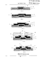
图2-8依次示出了本发明实施例一中的薄膜晶体管的主要制作工艺步骤,其中:
图2为栅电极形成的工艺步骤;
图3为栅介质层形成的工艺步骤;
图4为金属氧化物半导体层及将其进行热处理的工艺步骤;
图5对金属氧化物进行处理形成有源层的工艺步骤;
图6为涂布光刻胶,光刻胶图形化然后将沟道区进行氧化处理的工艺步骤;
图7为钝化层淀积和开接触孔的工艺步骤;
图8为生成源漏和栅电极引线的工艺步骤;
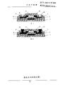
图9-16依次示出了本发明实施例二中的薄膜晶体管的主要制作工艺步骤,其中:
图9为栅电极形成的工艺步骤;
图10为栅介质层形成的工艺步骤;
图11为金属氧化物半导体层及将其进行热处理的工艺步骤;
图12为介质保护层淀积及金属氧化物半导体层和介质保护层图形化的工艺步骤;
图13为介质保护层图形化使沟道区露出的工艺步骤图;
图14为沟道区通过氧等离子体进行处理的工艺步骤;
图15为钝化层淀积和开接触孔的工艺步骤;
图16为生成源漏和栅电极引线的工艺步骤;
在本发明实施例中,薄膜晶体管的有源层采用具有高载流子浓度金属氧化物半导体层形成,生成有源层后,将源漏区保护起来,而将沟道区裸露于具有氧化功能的等离子体气氛,如氧等离子气氛中,使得沟道区氧空位浓度显著减少,成为低载流子浓度的高阻层。
下面通过具体实施方式结合附图对本发明作进一步详细说明。
请参考图1,图1所示为一种实施例中的薄膜晶体管的剖面结构示意图。薄膜晶体管包括一栅电极2,一栅介质层3,一金属氧化物半导体层4,金属氧化物半导体层4由一沟道区5,一源区6和一漏区7三部分组成,栅电极2位于衬底1之上,栅介质层3位于衬底1和栅电极2之上且将栅电极2覆盖,金属氧化物半导体层4位于栅介质3之上,沟道区5为金属氧化物半导体层4的中间部分,位于覆盖栅电极2的栅介质3之上,源区6和漏区7为金属氧化物半导体层4的两端部分,也分别位于栅介质3之上,且分别与沟道区5相连接。
本实施例中,栅电极2可为金属材料,如铬、钼、钛或铝等,其生成方法例如可采用磁控溅射方法或热蒸发方法;在另一实施例中,栅电极2也可为透明导电薄膜,如氧化铟锡(ITO)或氧化锌铝(AZO)等,其生成方法例如可采用磁控溅射方法。栅电极2的厚度一般为100~300纳米。栅介质3为氮化硅、氧化硅等绝缘介质,其生成方法例如可采用等离子增强化学汽相淀积PECVD或磁控溅射的方法;在另一实施例中,栅介质3也可为氧化铝、氧化钽或氧化铪等金属氧化物,其生成方法例如可采用磁控溅射方法。栅介质3的厚度一般为100~400纳米。金属氧化物半导体层4为非晶或多晶的金属氧化物半导体材料,如氧化锌基或氧化铟基的薄膜材料,其生成方法例如可采用磁控溅射方法,厚度为50~200纳米;沟道区5为有源层4的中间部分,其在未偏置状态下即零栅偏压状态下载流子浓度很低,呈现高电阻状态。源区6和漏区7为有源层4的两端部分,其载流子浓度很高,为低阻状态。
实施例一:
本实施例的薄膜晶体管的制作方法的步骤具体由图2至图8所示,包括以下步骤:
11)如图2所示,在衬底1的一面(例如正面)上生成一层100至300纳米厚的金属薄膜,生成该金属薄膜的方法可为磁控溅射法,其材料可为铬、钼、钛或铝等,然后将其进行相应的处理形成栅电极2,如可将其通过光刻和刻蚀形成栅电极2;本实施例中的衬底1可为耐高温的衬底,如玻璃衬底,也可为非耐高温的衬底,如塑料衬底。为描述方便,我们将衬底的制作薄膜晶体管的一面称为正面。
12)如图3所示,在衬底1正面上生成一层100至400纳米厚绝缘薄膜,该绝缘薄膜可为氮化硅、氧化硅等绝缘介质,可采用等离子增强化学汽相淀积(PECVD)方法生成该薄膜,并使其覆盖在上述栅电极2之上作为栅介质层3。
13)如图4所示,在栅介质层3上生成一层金属氧化物半导体层4,其厚度可为50至200纳米。其中,金属氧化物半导体层4为非晶或多晶的金属氧化物半导体材料,可采用磁控溅射法淀积该半导体层;如氧化锌基或氧化铟基的薄膜材料;当为氧化铟镓锌(IGZO)时,使用的靶由氧化镓、氧化铟和氧化锌的混合材料构成。三种材料的摩尔比为X:Y:Z,X.>40%,
Y>40, Z<20%, 其优选值为3:3:1。当为氧化铟时,所用的靶材为纯度等于或优于99.99%的氧化铟陶瓷靶。溅射气压在0.5~2.5
Pa之间,
气体为纯氩气。此时,所生成的整个金属氧化物半导体层4由于产生大量的氧空位,而呈现为高载流子浓度的低阻材料。若需要更加低阻的材料,可将其在无氧环境中进行热处理,如可将其置于氢气、氮气或真空中进行热处理,处理温度须低于衬底1所能承受的最高温度。
14)如图5所示,对金属氧化物半导体层4进行相应的处理以形成晶体管的有源区,有源区包括源区6、漏区7和沟道区5,处理方式可选为光刻和刻蚀方式。
15)如图6所示,在上述处理后的金属氧化物半导体层4上涂布光刻胶层,然后对其进行光刻,使所述金属氧化物半导体层4上的沟道区5露出,其余部分被光刻胶层覆盖保护。然后在低温下通过氧等离子体中进行氧化处理5~60分钟,由于沟道区5裸露在外被氧等离子氧化,其氧空位的浓度减低而转变成低载流子浓度。本实施例中的光刻胶层可为正性光刻胶层,也可为负性光刻胶层。本实施例中由于采用氧等离子体对其处理,可选择在低温下进行,如25到180度。氧化处理的温度的上限为光刻胶和衬底1能承受的最高温度。
16)如图7所示,用等离子增强化学汽相淀积(PECVD)或磁控溅射方法淀积一层100~300纳米厚的氮化硅层8,然后光刻和刻蚀形成电极的接触孔9和10。
17)如图8所示,用磁控溅射方法淀积一层100~300纳米厚的金属铝膜,然后光刻和刻蚀制成薄膜晶体管各电极的金属引出电极和互连线11和12。
本实施例中将沟道区5在低温下通过氧等离子体对其进行氧化处理,因为等离子体中的自由基比与之相应的气体的活性高得多,如氧等离子体中的氧自由基的活性就比氧气分子的活性高出许多,因此在采用等离子体对沟道区5进行氧化处理时即使在低温下,沟道区5也能够被充分氧化,氧空位浓度减少,因此本实施例中的衬底1不仅可采用耐高温的衬底材料,还可采用低温的衬底材料。
实施例二:
由于本发明将沟道区5在低温下通过氧等离子体对其进行氧化处理,因此无需再生成介质保护层,简化了晶体管的制作工艺。但是氧等离子对起到保护作用的光刻胶层有一定的影响,直接利用光刻胶层作为保护层的优点在于工艺简单,但在处理过程中部分光刻胶可能会被氧等离子体打掉,不能严格保护源区和漏区的所有区域不被氧化到;因此,为了进一步实现更精确地对源漏区的保护,可生长一层介质保护层以保护源区和漏区,且生成的介质保护层还可进入高温环境,便于后续的工艺的制作,具体制作步骤如下:
21)如图9所示,在衬底1正面上生成一层100至300纳米厚的金属薄膜,该金属薄膜可为铬、钼、钛或铝等,生成方式可为磁控溅射,然后将其光刻和刻蚀形成栅电极2,本实施例中的衬底1可为耐高温衬底,也可为低温衬底。
22)如图10所示,在衬底1正面上采用等离子增强化学汽相淀积(PECVD)方法生成一层100至400纳米厚绝缘薄膜,该薄膜可为氮化硅、氧化硅等绝缘介质,并使其覆盖在上述栅电极2之上作为栅介质层3。
23)如图11所示,在栅介质层3上采用射频磁控溅射淀积生成一层金属氧化物半导体层4,其厚度可为50至200纳米;其中,金属氧化物半导体层4为非晶或多晶的金属氧化物半导体材料,如氧化锌基或氧化铟基的薄膜材料;当为氧化铟镓锌(IGZO)时,使用的靶由氧化镓、氧化铟和氧化锌的混合材料构成。三种材料的摩尔比为X:Y:Z,X>40%,
Y>40, Z<20%, 其优选值为3:3:1。当为氧化铟时,所用的靶材为纯度等于或优于99.99%的氧化铟陶瓷靶。溅射气压在0.5~2.5
Pa之间,
气体为纯氩气。此时,所生成的整个金属氧化物半导体层4由于产生大量的氧空位,而呈现为高载流子浓度的低阻材料。若需要更加低阻的材料,可将其在无氧环境中进行热处理,如可将其置于氢气、氮气或真空中进行热处理,处理温度须低于衬底1能承受的最高温度。
24)如图12所示,在经步骤23处理后的金属氧化物半导体层4上生成一层介质保护膜,该介质保护膜可为氧化硅或氮化硅,生成的方法可采用等离子增强化学汽相淀积(PECVD)或磁控溅射的方法,其厚度为20至80纳米,光刻和刻蚀该介质保护层和金属氧化物半导体层4以形成晶体管的有源区保护层41和有源区,有源区包括源区6、漏区7和沟道区5。
25)如图13和14所示,在上述经光刻和刻蚀后的有源区保护层41上涂布光刻胶层,本实施例中的光刻胶层可为正性光刻胶层,也可为负性光刻胶层,然后对其进行光刻和刻蚀,使所述金属氧化物半导体层4上的沟道区5露出,其余部分被介质保护层保护。然后在低温下通过氧等离子体中进行氧化处理5~60分钟,由于沟道区5裸露在外被氧等离子氧化,其氧空位的浓度减低而转变成低载流子浓度。本实施例中由于采用氧等离子体对其处理,因此可在选择在低温下处理,如25到180度的温度下对其进行处理。值得注意的是,氧等离子体处理前,源漏区介质层上的光刻胶如果保留,则氧化处理的最高温度须低于衬底1和光刻胶能承受的最高温度。如光刻胶已去除,则氧化处理的最高温度须低于衬底1能承受的最高温度。
26)如图15所示,用等离子增强化学汽相淀积(PECVD)或磁控溅射方法淀积一层100~300纳米厚的氮化硅层8,然后光刻和刻蚀形成电极的接触孔9和10。
27)如图16所示,用磁控溅射方法淀积一层100~300纳米厚的金属铝膜,然后光刻和刻蚀制成薄膜晶体管各电极的金属引出电极和互连线11和12。
采用本发明实施例提供的方法制得的晶体管在源漏区具有高的载流子浓度的同时,其沟道区在零栅偏压下具有低的载流子浓度。同时,由于氧等离子体即使在低温下也有很强的氧化能力,在对沟道区进行氧化处理时,在低温(如25-180度)的环境中也可使其与氧等离子体发生充分的氧化反应,因此本发明中的衬底可选择为价格较低的低温衬底材料(如塑料衬底材料),处理过程可以在低温状态下进行,在进行相应的处理时,只要处理时的温度不超过衬底所能承受的最大温度即可,因此从原料和工艺两方面降低了薄膜晶体管的制造成本。
以上内容是结合具体的实施方式对本发明所作的进一步详细说明,不能认定本发明的具体实施只局限于这些说明。对于本发明所属技术领域的普通技术人员来说,在不脱离本发明构思的前提下,还可以做出若干简单推演或替换,都应当视为属于本发明的保护范围。
Claims (7)
- 一种薄膜晶体管的制作方法,其特征在于包括:栅电极生成步骤:在衬底上生成金属或透明导电薄膜作为栅电极;栅介质层生成步骤:在衬底上生成覆盖在所述栅电极之上的栅介质层;有源区生成及处理步骤:在栅介质层上生成一层具有高载流子浓度的金属氧化物半导体层,对其进行处理形成包括源区、漏区以及沟道区的有源区,将所述沟道区在低于所述衬底所能承受的最高温度的温度范围内通过具有氧化功能的等离子体进行氧化处理;电极引出步骤:生成源区、漏区和栅电极的电极引线。
- 如权利要求1所述的方法,其特征在于,所述具有氧化功能的等离子体为氧等离子体。
- 如权利要求1所述的方法,其特征在于,所述有源区生成及处理步骤中对所述金属氧化物半导体层进行处理形成有源区之前,还包括对所述金属氧化物半导体层在无氧环境中进行热处理。
- 如权利要求1所述的方法,其特征在于,在有源区生成及处理步骤中,在形成有源区的金属氧化物半导体层上直接涂光刻胶层,并进行光刻,使所述金属氧化物半导体层上的沟道区露出,然后在25-180度的温度下通过具有氧化功能的等离子体对其进行氧化处理。
- 如权利要求1所述的方法,其特征在于,在有源区生成及处理步骤中,在形成有源区的金属氧化物半导体层上先生成一层介质保护层,然后涂光刻胶层,接着光刻和刻蚀所述介质保护层使所述金属氧化物半导体层的沟道区露出,并在低于衬底所能承受的温度内通过具有氧化功能的氧等离子体对其进行处理。
- 如权利要求1所述的方法,其特征在于,所述衬底为耐高温衬底或者低温衬底。
- 如权利要求1所述的方法,其特征在于,所述金属氧化物半导体层的材料为氧化锌基或者氧化铟基材料。
Priority Applications (1)
| Application Number | Priority Date | Filing Date | Title |
|---|---|---|---|
| US13/376,833 US20130122649A1 (en) | 2011-01-18 | 2011-06-13 | Method for manufacturing thin film transistor |
Applications Claiming Priority (2)
| Application Number | Priority Date | Filing Date | Title |
|---|---|---|---|
| CN201110020661.7 | 2011-01-18 | ||
| CN2011100206617A CN102157565A (zh) | 2011-01-18 | 2011-01-18 | 一种薄膜晶体管的制作方法 |
Publications (1)
| Publication Number | Publication Date |
|---|---|
| WO2012097563A1 true WO2012097563A1 (zh) | 2012-07-26 |
Family
ID=44438897
Family Applications (1)
| Application Number | Title | Priority Date | Filing Date |
|---|---|---|---|
| PCT/CN2011/075649 Ceased WO2012097563A1 (zh) | 2011-01-18 | 2011-06-13 | 一种薄膜晶体管的制作方法 |
Country Status (3)
| Country | Link |
|---|---|
| US (1) | US20130122649A1 (zh) |
| CN (1) | CN102157565A (zh) |
| WO (1) | WO2012097563A1 (zh) |
Cited By (1)
| Publication number | Priority date | Publication date | Assignee | Title |
|---|---|---|---|---|
| CN103050441A (zh) * | 2012-12-10 | 2013-04-17 | 华映视讯(吴江)有限公司 | 氧化物薄膜晶体管制程方法 |
Families Citing this family (14)
| Publication number | Priority date | Publication date | Assignee | Title |
|---|---|---|---|---|
| CN103022142A (zh) * | 2011-09-27 | 2013-04-03 | 鸿富锦精密工业(深圳)有限公司 | 薄膜晶体管 |
| TWI486563B (zh) * | 2012-08-16 | 2015-06-01 | E Ink Holdings Inc | 光感測器及其光電晶體的驅動方法 |
| US9012261B2 (en) * | 2013-03-13 | 2015-04-21 | Intermolecular, Inc. | High productivity combinatorial screening for stable metal oxide TFTs |
| CN103325840B (zh) * | 2013-04-15 | 2016-05-18 | 北京大学深圳研究生院 | 薄膜晶体管及其制作方法 |
| CN104124277B (zh) * | 2013-04-24 | 2018-02-09 | 北京京东方光电科技有限公司 | 一种薄膜晶体管及其制作方法和阵列基板 |
| CN104681622A (zh) * | 2013-11-27 | 2015-06-03 | 北京大学 | 一种非晶氧化锌基薄膜晶体管及其制备方法 |
| CN104299915B (zh) | 2014-10-21 | 2017-03-22 | 北京大学深圳研究生院 | 金属氧化物薄膜晶体管制备方法 |
| CN106057679A (zh) * | 2016-06-17 | 2016-10-26 | 深圳市华星光电技术有限公司 | 氧化物半导体薄膜晶体管的制作方法 |
| CN106128963B (zh) | 2016-09-23 | 2019-07-23 | 京东方科技集团股份有限公司 | 薄膜晶体管及制备方法、阵列基板及制备方法、显示面板 |
| CN107836039A (zh) * | 2016-11-23 | 2018-03-23 | 深圳市柔宇科技有限公司 | 阵列基板的制造方法 |
| US20200194572A1 (en) * | 2016-11-23 | 2020-06-18 | Shenzhen Royole Technologies Co., Ltd. | ARRAY SUBSTRATE AND METHOD FOR MANUFACTURING ARRAY SUBSTRATE (As Amended) |
| KR102676341B1 (ko) * | 2016-12-30 | 2024-06-17 | 엘지디스플레이 주식회사 | 박막 트랜지스터, 그의 제조방법, 및 그를 포함한 표시장치 |
| CN114823349A (zh) * | 2022-01-26 | 2022-07-29 | 海宁市产业技术研究院 | 一种基于等离子体处理有源层的金属氧化物薄膜晶体管及其制备方法 |
| CN115497831B (zh) * | 2022-09-23 | 2023-06-20 | 西安工程大学 | 室温优化非晶铟镓锌氧薄膜晶体管界面的方法 |
Citations (3)
| Publication number | Priority date | Publication date | Assignee | Title |
|---|---|---|---|---|
| CN101478005A (zh) * | 2009-02-13 | 2009-07-08 | 北京大学深圳研究生院 | 一种金属氧化物薄膜晶体管及其制作方法 |
| JP2010062229A (ja) * | 2008-09-01 | 2010-03-18 | Semiconductor Energy Lab Co Ltd | 薄膜トランジスタ及び薄膜トランジスタの作製方法 |
| CN101728424A (zh) * | 2008-10-24 | 2010-06-09 | 株式会社半导体能源研究所 | 氧化物半导体、薄膜晶体管和显示装置 |
Family Cites Families (9)
| Publication number | Priority date | Publication date | Assignee | Title |
|---|---|---|---|---|
| KR0152529B1 (ko) * | 1990-03-27 | 1998-10-01 | 이헌조 | 플라즈마 산화를 이용한 박막 fet 트랜지스터의 제조방법 |
| US5470769A (en) * | 1990-03-27 | 1995-11-28 | Goldstar Co., Ltd. | Process for the preparation of a thin film transistor |
| CN1324665C (zh) * | 2004-03-29 | 2007-07-04 | 广辉电子股份有限公司 | 自对准式薄膜晶体管的制造方法 |
| KR101410926B1 (ko) * | 2007-02-16 | 2014-06-24 | 삼성전자주식회사 | 박막 트랜지스터 및 그 제조방법 |
| KR101510212B1 (ko) * | 2008-06-05 | 2015-04-10 | 삼성전자주식회사 | 산화물 반도체 박막 트랜지스터의 제조방법 |
| TWI489628B (zh) * | 2009-04-02 | 2015-06-21 | 半導體能源研究所股份有限公司 | 半導體裝置和其製造方法 |
| CN101533779A (zh) * | 2009-04-03 | 2009-09-16 | 北京大学深圳研究生院 | 一种薄膜晶体管及图像显示装置的制作方法 |
| SG10201403913PA (en) * | 2009-07-10 | 2014-10-30 | Semiconductor Energy Lab | Method for manufacturing semiconductor device |
| KR101768786B1 (ko) * | 2009-07-18 | 2017-08-16 | 가부시키가이샤 한도오따이 에네루기 켄큐쇼 | 반도체 장치 및 반도체 장치의 제조 방법 |
-
2011
- 2011-01-18 CN CN2011100206617A patent/CN102157565A/zh active Pending
- 2011-06-13 US US13/376,833 patent/US20130122649A1/en not_active Abandoned
- 2011-06-13 WO PCT/CN2011/075649 patent/WO2012097563A1/zh not_active Ceased
Patent Citations (3)
| Publication number | Priority date | Publication date | Assignee | Title |
|---|---|---|---|---|
| JP2010062229A (ja) * | 2008-09-01 | 2010-03-18 | Semiconductor Energy Lab Co Ltd | 薄膜トランジスタ及び薄膜トランジスタの作製方法 |
| CN101728424A (zh) * | 2008-10-24 | 2010-06-09 | 株式会社半导体能源研究所 | 氧化物半导体、薄膜晶体管和显示装置 |
| CN101478005A (zh) * | 2009-02-13 | 2009-07-08 | 北京大学深圳研究生院 | 一种金属氧化物薄膜晶体管及其制作方法 |
Cited By (1)
| Publication number | Priority date | Publication date | Assignee | Title |
|---|---|---|---|---|
| CN103050441A (zh) * | 2012-12-10 | 2013-04-17 | 华映视讯(吴江)有限公司 | 氧化物薄膜晶体管制程方法 |
Also Published As
| Publication number | Publication date |
|---|---|
| US20130122649A1 (en) | 2013-05-16 |
| CN102157565A (zh) | 2011-08-17 |
Similar Documents
| Publication | Publication Date | Title |
|---|---|---|
| WO2012097563A1 (zh) | 一种薄膜晶体管的制作方法 | |
| WO2012097564A1 (zh) | 一种自对准薄膜晶体管的制作方法 | |
| WO2014169621A1 (zh) | 薄膜晶体管及其制作方法 | |
| WO2013013599A1 (zh) | 阵列基板及其制作方法、液晶面板、显示装置 | |
| CN101478005A (zh) | 一种金属氧化物薄膜晶体管及其制作方法 | |
| WO2012071878A1 (zh) | 一种晶体管的制造方法 | |
| WO2010100885A1 (en) | Method for forming semiconductor film, method for forming semiconductor device and semiconductor device | |
| CN103346089B (zh) | 一种自对准双层沟道金属氧化物薄膜晶体管及其制作方法 | |
| WO2014012334A1 (zh) | 阵列基板的制造方法及阵列基板、显示装置 | |
| WO2016201729A1 (zh) | 一种阵列基板及其制作方法、液晶显示器 | |
| JPWO2010024279A1 (ja) | 電界効果型トランジスタの製造方法及び製造装置 | |
| WO2016119280A1 (zh) | 氧化物薄膜晶体管及其制作方法 | |
| CN103972299B (zh) | 一种薄膜晶体管及其制作方法、显示基板、显示装置 | |
| WO2017054191A1 (zh) | 一种tft阵列基板及其制作方法 | |
| WO2020171341A1 (ko) | 질소-도핑된 그래핀층을 활성층으로 포함하는 그래핀 기반의 tft | |
| WO2018205318A1 (zh) | 一种tft阵列基板及其制作方法 | |
| WO2017054258A1 (zh) | Tft阵列基板的制备方法、tft阵列基板及显示装置 | |
| CN112397573A (zh) | 一种阵列基板及其制备方法、显示面板 | |
| CN103337462B (zh) | 一种薄膜晶体管的制备方法 | |
| WO2015182888A1 (ko) | 산화물 반도체 박막 트랜지스터의 제조방법 | |
| CN104505405A (zh) | 薄膜晶体管及制备方法、阵列基板及制备方法、显示装置 | |
| CN104576760A (zh) | 薄膜晶体管及其制备方法、阵列基板和显示装置 | |
| WO2017140015A1 (zh) | 双栅极tft阵列基板及制作方法 | |
| WO2023106781A1 (ko) | 스피넬 단일 결정상의 izto 산화물 반도체를 구비하는 박막트랜지스터 | |
| CN114447119B (zh) | Tft基板及其制作方法 |
Legal Events
| Date | Code | Title | Description |
|---|---|---|---|
| 121 | Ep: the epo has been informed by wipo that ep was designated in this application |
Ref document number: 11856030 Country of ref document: EP Kind code of ref document: A1 |
|
| WWE | Wipo information: entry into national phase |
Ref document number: 13376833 Country of ref document: US |
|
| NENP | Non-entry into the national phase |
Ref country code: DE |
|
| 122 | Ep: pct application non-entry in european phase |
Ref document number: 11856030 Country of ref document: EP Kind code of ref document: A1 |