WO2012077585A1 - 積層セラミック電子部品 - Google Patents
積層セラミック電子部品 Download PDFInfo
- Publication number
- WO2012077585A1 WO2012077585A1 PCT/JP2011/077887 JP2011077887W WO2012077585A1 WO 2012077585 A1 WO2012077585 A1 WO 2012077585A1 JP 2011077887 W JP2011077887 W JP 2011077887W WO 2012077585 A1 WO2012077585 A1 WO 2012077585A1
- Authority
- WO
- WIPO (PCT)
- Prior art keywords
- pair
- multilayer ceramic
- thickness
- outer layer
- less
- Prior art date
- Legal status (The legal status is an assumption and is not a legal conclusion. Google has not performed a legal analysis and makes no representation as to the accuracy of the status listed.)
- Ceased
Links
Images



Classifications
-
- H—ELECTRICITY
- H01—ELECTRIC ELEMENTS
- H01G—CAPACITORS; CAPACITORS, RECTIFIERS, DETECTORS, SWITCHING DEVICES, LIGHT-SENSITIVE OR TEMPERATURE-SENSITIVE DEVICES OF THE ELECTROLYTIC TYPE
- H01G4/00—Fixed capacitors; Processes of their manufacture
- H01G4/002—Details
- H01G4/018—Dielectrics
- H01G4/06—Solid dielectrics
- H01G4/08—Inorganic dielectrics
- H01G4/12—Ceramic dielectrics
- H01G4/1209—Ceramic dielectrics characterised by the ceramic dielectric material
-
- H—ELECTRICITY
- H01—ELECTRIC ELEMENTS
- H01G—CAPACITORS; CAPACITORS, RECTIFIERS, DETECTORS, SWITCHING DEVICES, LIGHT-SENSITIVE OR TEMPERATURE-SENSITIVE DEVICES OF THE ELECTROLYTIC TYPE
- H01G4/00—Fixed capacitors; Processes of their manufacture
- H01G4/002—Details
- H01G4/258—Temperature compensation means
-
- H—ELECTRICITY
- H01—ELECTRIC ELEMENTS
- H01G—CAPACITORS; CAPACITORS, RECTIFIERS, DETECTORS, SWITCHING DEVICES, LIGHT-SENSITIVE OR TEMPERATURE-SENSITIVE DEVICES OF THE ELECTROLYTIC TYPE
- H01G4/00—Fixed capacitors; Processes of their manufacture
- H01G4/002—Details
- H01G4/005—Electrodes
-
- H—ELECTRICITY
- H01—ELECTRIC ELEMENTS
- H01G—CAPACITORS; CAPACITORS, RECTIFIERS, DETECTORS, SWITCHING DEVICES, LIGHT-SENSITIVE OR TEMPERATURE-SENSITIVE DEVICES OF THE ELECTROLYTIC TYPE
- H01G4/00—Fixed capacitors; Processes of their manufacture
- H01G4/002—Details
- H01G4/005—Electrodes
- H01G4/012—Form of non-self-supporting electrodes
-
- H—ELECTRICITY
- H01—ELECTRIC ELEMENTS
- H01G—CAPACITORS; CAPACITORS, RECTIFIERS, DETECTORS, SWITCHING DEVICES, LIGHT-SENSITIVE OR TEMPERATURE-SENSITIVE DEVICES OF THE ELECTROLYTIC TYPE
- H01G4/00—Fixed capacitors; Processes of their manufacture
- H01G4/002—Details
- H01G4/018—Dielectrics
- H01G4/06—Solid dielectrics
- H01G4/08—Inorganic dielectrics
- H01G4/12—Ceramic dielectrics
-
- H—ELECTRICITY
- H01—ELECTRIC ELEMENTS
- H01G—CAPACITORS; CAPACITORS, RECTIFIERS, DETECTORS, SWITCHING DEVICES, LIGHT-SENSITIVE OR TEMPERATURE-SENSITIVE DEVICES OF THE ELECTROLYTIC TYPE
- H01G4/00—Fixed capacitors; Processes of their manufacture
- H01G4/30—Stacked capacitors
-
- H—ELECTRICITY
- H05—ELECTRIC TECHNIQUES NOT OTHERWISE PROVIDED FOR
- H05K—PRINTED CIRCUITS; CASINGS OR CONSTRUCTIONAL DETAILS OF ELECTRIC APPARATUS; MANUFACTURE OF ASSEMBLAGES OF ELECTRICAL COMPONENTS
- H05K3/00—Apparatus or processes for manufacturing printed circuits
- H05K3/10—Apparatus or processes for manufacturing printed circuits in which conductive material is applied to the insulating support in such a manner as to form the desired conductive pattern
- H05K3/12—Apparatus or processes for manufacturing printed circuits in which conductive material is applied to the insulating support in such a manner as to form the desired conductive pattern using thick film techniques, e.g. printing techniques to apply the conductive material or similar techniques for applying conductive paste or ink patterns
- H05K3/1283—After-treatment of the printed patterns, e.g. sintering or curing methods
- H05K3/1291—Firing or sintering at relative high temperatures for patterns on inorganic boards, e.g. co-firing of circuits on green ceramic sheets
-
- H—ELECTRICITY
- H05—ELECTRIC TECHNIQUES NOT OTHERWISE PROVIDED FOR
- H05K—PRINTED CIRCUITS; CASINGS OR CONSTRUCTIONAL DETAILS OF ELECTRIC APPARATUS; MANUFACTURE OF ASSEMBLAGES OF ELECTRICAL COMPONENTS
- H05K3/00—Apparatus or processes for manufacturing printed circuits
- H05K3/46—Manufacturing multilayer circuits
- H05K3/4611—Manufacturing multilayer circuits by laminating two or more circuit boards
- H05K3/4626—Manufacturing multilayer circuits by laminating two or more circuit boards characterised by the insulating layers or materials
- H05K3/4629—Manufacturing multilayer circuits by laminating two or more circuit boards characterised by the insulating layers or materials laminating inorganic sheets comprising printed circuits, e.g. green ceramic sheets
-
- H—ELECTRICITY
- H05—ELECTRIC TECHNIQUES NOT OTHERWISE PROVIDED FOR
- H05K—PRINTED CIRCUITS; CASINGS OR CONSTRUCTIONAL DETAILS OF ELECTRIC APPARATUS; MANUFACTURE OF ASSEMBLAGES OF ELECTRICAL COMPONENTS
- H05K3/00—Apparatus or processes for manufacturing printed circuits
- H05K3/46—Manufacturing multilayer circuits
- H05K3/4644—Manufacturing multilayer circuits by building the multilayer layer by layer, i.e. build-up multilayer circuits
- H05K3/4664—Adding a circuit layer by thick film methods, e.g. printing techniques or by other techniques for making conductive patterns by using pastes, inks or powders
-
- H—ELECTRICITY
- H05—ELECTRIC TECHNIQUES NOT OTHERWISE PROVIDED FOR
- H05K—PRINTED CIRCUITS; CASINGS OR CONSTRUCTIONAL DETAILS OF ELECTRIC APPARATUS; MANUFACTURE OF ASSEMBLAGES OF ELECTRICAL COMPONENTS
- H05K1/00—Printed circuits
- H05K1/16—Printed circuits incorporating printed electric components, e.g. printed resistors, capacitors or inductors
- H05K1/162—Printed circuits incorporating printed electric components, e.g. printed resistors, capacitors or inductors incorporating printed capacitors
-
- H—ELECTRICITY
- H05—ELECTRIC TECHNIQUES NOT OTHERWISE PROVIDED FOR
- H05K—PRINTED CIRCUITS; CASINGS OR CONSTRUCTIONAL DETAILS OF ELECTRIC APPARATUS; MANUFACTURE OF ASSEMBLAGES OF ELECTRICAL COMPONENTS
- H05K3/00—Apparatus or processes for manufacturing printed circuits
- H05K3/10—Apparatus or processes for manufacturing printed circuits in which conductive material is applied to the insulating support in such a manner as to form the desired conductive pattern
- H05K3/12—Apparatus or processes for manufacturing printed circuits in which conductive material is applied to the insulating support in such a manner as to form the desired conductive pattern using thick film techniques, e.g. printing techniques to apply the conductive material or similar techniques for applying conductive paste or ink patterns
- H05K3/1216—Apparatus or processes for manufacturing printed circuits in which conductive material is applied to the insulating support in such a manner as to form the desired conductive pattern using thick film techniques, e.g. printing techniques to apply the conductive material or similar techniques for applying conductive paste or ink patterns by screen printing or stencil printing
Definitions
- the present invention relates to a multilayer ceramic electronic component, and more particularly to an improvement for improving the thermal shock resistance of the multilayer ceramic electronic component.
- Patent Document 1 Japanese Unexamined Patent Application Publication No. 2005-136132 describes a technique for making a multilayer ceramic capacitor resistant to thermal stress.
- dielectric layers are arranged in layers between a plurality of internal electrodes, and these are laminated along the laminating direction, and a dielectric is arranged on the outer peripheral side of the plurality of internal electrodes.
- the laminated body formed as described above is a multilayer ceramic capacitor having a main body portion, and is the most on the end face (main surface) located in the lamination direction of the laminate and the end face (main surface) located in the lamination direction.
- a pair of upper and lower margin portions (outer layer portions) in which no internal electrode exists are respectively disposed between the inner electrode and the inner electrode, and an end surface (side surface) positioned in a direction intersecting the stacking direction of the stacked body and the inner electrode
- a pair of left and right margin portions (width direction gap portions) in which no internal electrode is present are respectively disposed between the end portions, the dimensions of the upper and lower margin portions (outer layer portions), and the left and right margin portions (width direction gap portions).
- Dimensions are The difference between the dimensions of the upper and lower margin parts (outer layer part) and the left and right margin parts (width direction gap part) is within 20% of the dimensions of the upper and lower margin parts (outer layer part).
- a multilayer ceramic capacitor that is resistant to thermal stress can be obtained even when a large number of internal electrodes are stacked.
- a thermal shock is applied to the multilayer ceramic capacitor, for example, during solder reflow mounting.
- a thermal stress test at 280 ° C. is performed. If it can withstand, it can withstand thermal shock during solder reflow mounting.
- the multilayer ceramic capacitor has been described above, but the same problem can be encountered with multilayer ceramic electronic components other than the multilayer ceramic capacitor.
- an object of the present invention is to provide a multilayer ceramic electronic component capable of realizing a higher level of thermal shock resistance.
- the present invention includes a laminated body including a plurality of laminated ceramic layers and a plurality of internal electrodes located between the ceramic layers, and the laminated body extends in the extending direction of the ceramic layers and faces a pair of main surfaces, And a pair of opposite side surfaces and a pair of opposite end surfaces respectively extending in a direction orthogonal to the main surface, and the internal electrode is drawn out to any one of the pair of end surfaces, Laminations distributed in regions located across the gap in the width direction with respect to each of the pair of side surfaces, and distributed in regions located through the outer layer thickness with respect to each of the pair of main surfaces Directed to ceramic electronic components.
- the present invention provides a first condition that the thickness of the internal electrode is 0.4 ⁇ m or less, and a width.
- the second condition is that the directional gap is 30 ⁇ m or less, or the outer layer thickness is 35 ⁇ m or less.
- the first condition that the thickness of the internal electrode is 0.4 ⁇ m or less is the same as in the case of the first aspect, but the second condition is that the width direction gap is 30 ⁇ m or less.
- the outer layer thickness is 35 ⁇ m or less.
- the third condition in addition to the first and second conditions in the first or second aspect, the third condition further satisfies the third condition that the coverage of the internal electrode is 75% or more. To be done.
- the multilayer ceramic electronic component according to the present invention is used, for example, in the vicinity of an engine room of an automobile, or when a substrate after mounting the multilayer ceramic electronic component is further joined to some base material by welding or the like. Can withstand well.
- the thermal shock of a higher load can be endured than when the condition according to the first aspect is satisfied, and further, the third aspect described above.
- the condition by is satisfied, it is possible to withstand a higher thermal shock than when the condition by the second aspect is satisfied.
- the size of the upper and lower margin portions (outer layer portion) and the size of the left and right margin portions (width direction gap portion) should be larger than 50 ⁇ m. Therefore, even if a crack due to thermal stress occurs, the idea of preventing it from reaching the capacitance forming portion appears.
- the present invention by reducing the thickness of the internal electrode to 0.4 ⁇ m or less, suppressing the generation of stress due to the difference in the thermal expansion coefficient described above, the width direction gap and / or the outer layer thickness, Contrary to the case of Patent Document 1, the occurrence of structural defects such as cracks during thermal shock is suppressed by reducing the size. That is, the idea is to reduce the stress itself generated due to thermal stress and suppress the generation of cracks as much as possible.
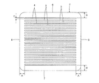
- FIG. 1 is a cross-sectional view illustrating a multilayer ceramic capacitor as an example of a multilayer ceramic electronic component according to an embodiment of the present invention.
- FIG. 2 is an enlarged sectional view taken along line II-II in FIG. While showing the distribution of the gap in the width direction and the thickness of the outer layer of the samples prepared in Experimental Example 1 with the thickness of the internal electrode of 0.4 ⁇ m, the evaluation results of defect occurrence for each sample are It is the figure displayed with the symbol. While showing the distribution of the gap in the width direction and the thickness of the outer layer of the samples prepared in Experimental Example 1 with the internal electrode thickness of 0.2 ⁇ m, the evaluation results of defect occurrence for each sample are It is the figure displayed with the symbol.
- the multilayer ceramic capacitor 1 includes a multilayer body 2 as a component body.
- the multilayer body 2 includes a plurality of laminated ceramic layers 3 and a plurality of internal electrodes 4 and 5 positioned between the ceramic layers 3.
- the internal electrodes 4 and the internal electrodes 5 are alternately arranged in the stacking direction.
- the laminate 2 extends in the extending direction of the ceramic layer 3 and faces a pair of main surfaces 6 and 7 and a pair of side surfaces facing each other extending in a direction perpendicular to the main surfaces 6 and 7. It has a rectangular parallelepiped shape or a substantially rectangular parallelepiped shape having 8 and 9 and a pair of end faces 10 and 11 facing each other.
- a plurality of internal electrodes 4 and 5 are drawn out from the end faces 10 and 11 of the laminate 2, respectively, and the respective end portions are exposed. The respective end portions of the internal electrodes 4 and the respective end portions of the internal electrode 5 are exposed.
- the external electrodes 12 and 13 are formed so as to be electrically connected to each other.
- the internal electrodes 4 and 5 are distributed in a region located via a predetermined width direction gap A with respect to each of the pair of side surfaces 8 and 9, and a pair of main surfaces
- Each of 6 and 7 is distributed in a region located through a predetermined outer layer thickness B.
- the second condition that the thickness B is 35 ⁇ m or less is satisfied.
- both the width direction gap A is 30 ⁇ m or less and the outer layer thickness B is 35 ⁇ m or less.
- the third condition that the coverage of the internal electrodes 4 and 5 is 75% or more is satisfied.
- the lower limit of the thickness C of each of the internal electrodes 4 and 5 is about 0.05 ⁇ m
- the outer layer thickness B is about 5 ⁇ m
- the width direction gap A is about 5 ⁇ m.
- a ceramic green sheet to be the ceramic layer 3 is prepared, and a conductive paste film to be the internal electrodes 4 and 5 is formed on the ceramic green sheet by printing. Is done.
- a plurality of ceramic green sheets are laminated to produce a green laminate that is to be a laminate 2 including a plurality of green ceramic layers and a conductive paste film positioned between the green ceramic layers.
- the thickness C of the internal electrodes 4 and 5 is made as thin as 0.4 ⁇ m or less in order to satisfy the first condition described above, it is not easy to satisfy the third condition that the coverage is maintained at 75% or more. For example, if the firing temperature is lowered, the coverage can be easily maintained at 75% or more, but on the other hand, the ceramic is not sufficiently sintered.
- a heat treatment step to which an average temperature rising rate up to the maximum temperature is applied is 40 ° C./second or more, preferably 100 ° C./second or more is applied.
- it is effective to cool without maintaining the temperature after reaching the maximum temperature.
- the unfired laminate is degreased before the above-described heat treatment step.
- the heat treatment step may be performed in an atmosphere in which an atmosphere gas on the oxidation side is supplied with respect to the equilibrium oxygen partial pressure of the base metal.
- the ceramic layer 3 is made of a dielectric ceramic.
- the present invention is not limited to a multilayer ceramic capacitor, but may be an inductor, a thermistor, a piezoelectric component, or the like. Therefore, according to the function of the multilayer ceramic electronic component, the ceramic layer may be composed of a dielectric ceramic, a magnetic ceramic, a semiconductor ceramic, a piezoelectric ceramic, or the like.
- the multilayer ceramic capacitor 1 shown in FIG. 1 is a two-terminal type having two external terminals 12 and 13, but the present invention can also be applied to a multi-terminal type multilayer ceramic electronic component. it can.
- Example 1 (1) Preparation of Sample A ceramic green sheet containing a ceramic powder mainly composed of barium titanate and an organic binder was formed on a base film so that the thickness after firing was 1 ⁇ m. Next, a conductive paste film to be an internal electrode was formed on the ceramic green sheet by screen printing so that the thickness shown in the column of “Internal electrode thickness” in Tables 1 and 2 was obtained after firing.
- the internal electrode has a width as shown in the column of “width direction gap” in Table 1 and Table 2. The dimensions were adjusted to be distributed in the region located through the directional gap.
- a predetermined number of green sheets on which the conductive paste film is formed are stacked so that the side where the conductive paste film is drawn is staggered, and further, the conductive paste film is formed so as to sandwich them.
- a predetermined number of green sheets for the outer layer portion that were not stacked were stacked and heated / pressurized to produce a laminate block.
- the number of laminated green sheets for the outer layer portion was adjusted so that the “outer layer thickness” in Tables 1 and 2 was obtained after firing.
- the laminated body block was cut with a dicing saw to obtain an unfired laminated body.
- the obtained unfired laminate was degreased by heat treatment at a maximum temperature of 240 ° C. in an N 2 airflow. Subsequently, firing was performed at a maximum temperature of 1180 ° C. in an N 2 —H 2 O—H 2 gas stream in an atmosphere having an oxygen partial pressure of 10 ⁇ 9.5 MPa.
- the external electrode was formed on the end surface portion from which the internal electrode was drawn out of the sintered laminate thus obtained. More specifically, a conductive paste mainly composed of copper was applied and baked at 800 ° C. to form a base layer, and a Ni plating film and a Sn plating film were formed thereon by wet plating.
- the obtained multilayer ceramic capacitor was confirmed to have the values of “internal electrode thickness”, “outer layer thickness”, and “width gap” shown in Tables 1 and 2 as follows.
- the group of internal electrodes was divided into three equal parts with respect to the thickness direction of the sample, and was classified into three regions: an upper region, a middle region, and a lower region.
- a perpendicular line was drawn perpendicular to the internal electrode and dividing the internal electrode into two in the width direction.
- 25 layers of internal electrodes were selected from the center of each of the three regions, and the thicknesses of these internal electrodes on the perpendicular were measured.
- the thickness of the internal electrode was measured at 75 locations for one sample, the thickness of the internal electrode was determined at a total of 225 locations of the three samples, and the average value thereof was determined. However, no count was made for locations where the internal electrodes were missing.
- multilayer ceramic capacitors were prepared for each sample.
- the resin was hardened so that the side surfaces were upright, and the side surfaces were polished along the width direction of the multilayer ceramic capacitors to obtain a polished cross section at half the width direction.
- ion milling was performed on the polished cross section to remove sagging due to polishing. In this way, a second cross section for observation was obtained.
- the average value of the outer layer thicknesses at a total of 60 locations for a total of six samples was obtained.
- the outer layer thickness of each sample was a value as shown in the column of “outer layer thickness” in Tables 1 and 2 as intended.
- FIG. 3 and 4 show the distribution state of the gap in the width direction and the outer layer thickness for a specific sample, and the evaluation results of the occurrence of defects are indicated by symbols ⁇ and ⁇ .
- FIG. 3 shows the samples 37 to 55 shown in Table 2 in which the thickness of the internal electrode is 0.4 ⁇ m.
- FIG. 4 shows the samples 56 to 65 shown in Table 2 with the internal electrode thickness of 0.2 ⁇ m.
- FIGS. 3 and 4 when the defect occurrence rate is not 0% (particularly, when the defect occurrence rate is 100% in FIG. 3), it is indicated by ⁇ , and when it is 0%, it is indicated by ⁇ . Comparing FIG. 3 and FIG. 4, it can be seen that the same tendency appears as when the thickness of the internal electrode is 0.4 ⁇ m even when the thickness of the internal electrode is 0.4 ⁇ m.
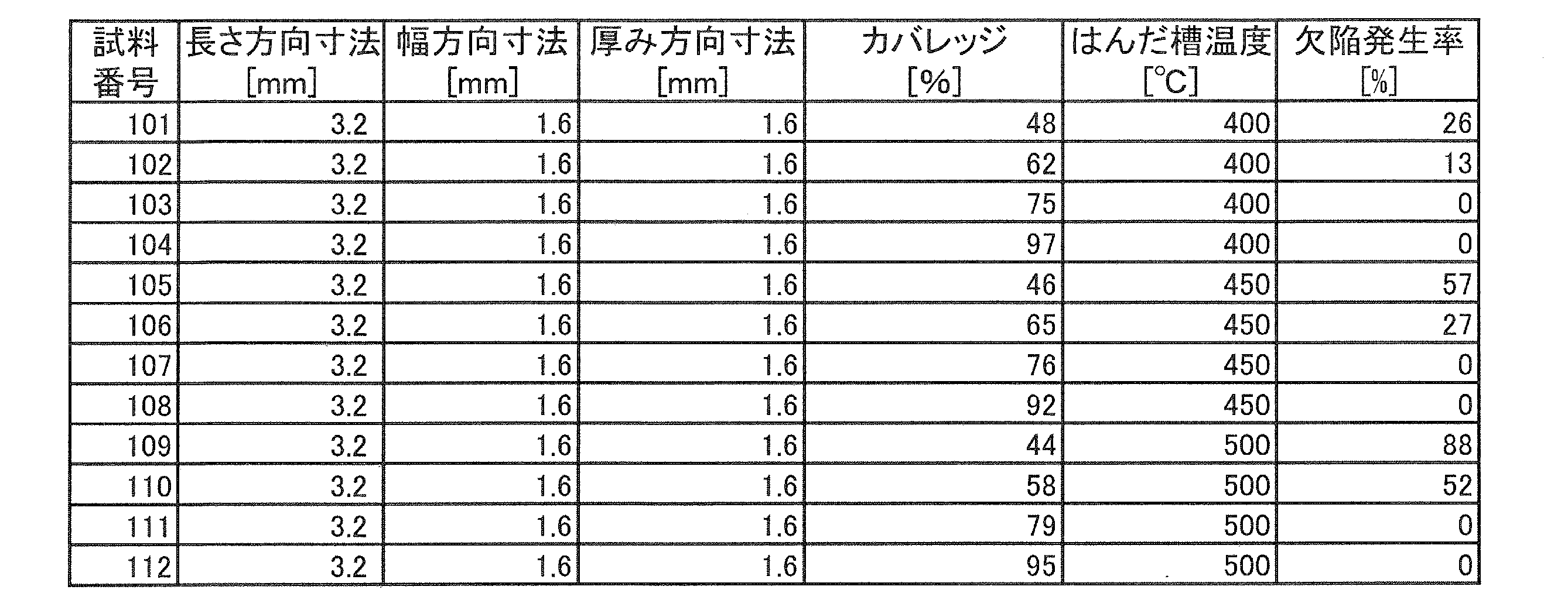
- the multilayer ceramic capacitor according to each sample having the outer dimensions shown in “Lengthwise dimension”, “Widthwise dimension”, and “Thickness direction dimension” in Table 3 through basically the same steps as in Experimental Example 1 Got. All the multilayer ceramic capacitors according to each sample had an internal electrode thickness of 0.4 ⁇ m, a width direction gap of 30 ⁇ m, and an outer layer thickness of 35 ⁇ m. Then, by controlling the maximum temperature in the firing step between 1100 ° C. and 1300 ° C., the coverage of the internal electrodes was changed as shown in the “Coverage” column of Table 3.
- the “coverage” is higher. More specifically, when the “solder bath temperature” is 450 ° C., the “coverage” is 76% or more, and the “defect occurrence rate” When the “solder bath temperature” is 500 ° C., the “coverage” is 79% or more and the “defect occurrence rate” is 0%.
Landscapes
- Engineering & Computer Science (AREA)
- Power Engineering (AREA)
- Manufacturing & Machinery (AREA)
- Microelectronics & Electronic Packaging (AREA)
- Chemical & Material Sciences (AREA)
- Ceramic Engineering (AREA)
- Inorganic Chemistry (AREA)
- Fixed Capacitors And Capacitor Manufacturing Machines (AREA)
- Ceramic Capacitors (AREA)
Abstract
Description
(1)試料の作製
チタン酸バリウムを主成分とするセラミック粉末と有機バインダとを含むセラミックグリーンシートを、焼成後の厚みが1μmとなるようにベースフィルム上に成形した。次いで、上記セラミックグリーンシート上に、表1および表2の「内部電極の厚み」の欄に示す厚みが焼成後に得られるように、内部電極となるべき導電性ペースト膜をスクリーン印刷によって形成した。ここで、導電性ペースト膜の印刷パターンについては、後のカット工程および焼成工程を経て得られた積層体において、内部電極が表1および表2の「幅方向ギャップ」の欄に示すような幅方向ギャップを介して位置する領域に分布するように、その寸法を調整した。
各試料において、3つの積層セラミックコンデンサを用意した。これら積層セラミックコンデンサの端面が立つように樹脂固めを行ない、端面を積層セラミックコンデンサの長さ方向に沿って研磨し、長さ方向の1/2の時点における研磨断面を得た。次に、この研磨断面に対しイオンミリングを行ない、研磨によるダレを除去した。このようにして、観察用の断面を得た。
幅方向ギャップを求めるため、上記(1)で得た観察用の断面を用いた。内部電極の存在する領域を試料の厚み方向に対して6等分に分割する位置にある7層の内部電極を特定した。これら7層の内部電極のうち、最上層の内部電極と最下層の内部電極とを除いた5層の内部電極が位置する箇所において、幅方向ギャップを、右側および左側の両方において、計10箇所測定した。そして、計3つの試料の合計30箇所の幅方向ギャップの値を求め、これらの平均値を求めた。
外層厚みを求めるため、第1に、上記(1)で得た観察用の断面を用いた。内部電極に直交しかつ内部電極を幅方向に6等分する7本の垂線を引いた。これら7本の垂線のうち、両側2本の垂線を除いた5本の垂線上において、外層厚みを上側と下側の両側において、計10箇所測定した。そして、計3つの試料の合計30箇所の外層厚みをまず求めた。
各試料に係る積層セラミックコンデンサに対して、以下のように熱衝撃試験を実施した。


実験例2では、内部電極のカバレッジと熱衝撃試験による欠陥発生率との関係を評価した。
2 積層体
3 セラミック層
4,5 内部電極
6,7 主面
8,9 側面
10,11 端面
Claims (3)
- 積層された複数のセラミック層と前記セラミック層間に位置する複数の内部電極とを含む積層体を備え、
前記積層体は、前記セラミック層の延びる方向に延びかつ互いに対向する1対の主面、ならびに、前記主面に対して直交する方向にそれぞれ延びる、互いに対向する1対の側面および互いに対向する1対の端面を有し、
前記内部電極は、1対の前記端面のいずれか一方にまで引き出され、1対の前記側面の各々に対して幅方向ギャップを介して位置する領域に分布しており、かつ1対の前記主面の各々に対して外層厚みを介して位置する領域に分布している、
積層セラミック電子部品であって、
前記内部電極の厚みが0.4μm以下である、という第1の条件と、
前記幅方向ギャップが30μm以下である、または前記外層厚みが35μm以下である、という第2の条件と
を満たす、積層セラミック電子部品。 - 積層された複数のセラミック層と前記セラミック層間に位置する内部電極とを含む積層体を備え、
前記積層体は、前記セラミック層の延びる方向に延びかつ互いに対向する1対の主面、ならびに、前記主面に対して直交する方向にそれぞれ延びる、互いに対向する1対の側面および互いに対向する1対の端面を有し、
前記内部電極は、1対の前記端面のいずれか一方にまで引き出され、1対の前記側面の各々に対して幅方向ギャップを介して位置する領域に分布しており、かつ1対の前記主面の各々に対して外層厚みを介して位置する領域に分布している、
積層セラミック電子部品であって、
前記内部電極の厚みが0.4μm以下である、という第1の条件と、
前記幅方向ギャップが30μm以下である、および前記外層厚みが35μm以下である、という第2の条件と
を満たす、積層セラミック電子部品。 - さらに、前記内部電極のカバレッジが75%以上である、という第3の条件を満たす、請求項1または2に記載の積層セラミック電子部品。
Priority Applications (6)
| Application Number | Priority Date | Filing Date | Title |
|---|---|---|---|
| KR1020137014554A KR101541505B1 (ko) | 2010-12-06 | 2011-12-02 | 적층 세라믹 전자부품 |
| KR1020157001868A KR101589567B1 (ko) | 2010-12-06 | 2011-12-02 | 적층 세라믹 전자부품, 및 적층 세라믹 전자부품의 제조방법 |
| JP2012547817A JP5477479B2 (ja) | 2010-12-06 | 2011-12-02 | 積層セラミック電子部品 |
| CN201180058768.9A CN103250217B (zh) | 2010-12-06 | 2011-12-02 | 叠层陶瓷电子元件 |
| US13/856,475 US20130222972A1 (en) | 2010-12-06 | 2013-04-04 | Laminated ceramic electronic component |
| US15/172,199 US9972438B2 (en) | 2010-12-06 | 2016-06-03 | Laminated ceramic electronic component |
Applications Claiming Priority (2)
| Application Number | Priority Date | Filing Date | Title |
|---|---|---|---|
| JP2010-271097 | 2010-12-06 | ||
| JP2010271097 | 2010-12-06 |
Related Child Applications (1)
| Application Number | Title | Priority Date | Filing Date |
|---|---|---|---|
| US13/856,475 Continuation US20130222972A1 (en) | 2010-12-06 | 2013-04-04 | Laminated ceramic electronic component |
Publications (1)
| Publication Number | Publication Date |
|---|---|
| WO2012077585A1 true WO2012077585A1 (ja) | 2012-06-14 |
Family
ID=46207074
Family Applications (1)
| Application Number | Title | Priority Date | Filing Date |
|---|---|---|---|
| PCT/JP2011/077887 Ceased WO2012077585A1 (ja) | 2010-12-06 | 2011-12-02 | 積層セラミック電子部品 |
Country Status (6)
| Country | Link |
|---|---|
| US (2) | US20130222972A1 (ja) |
| JP (1) | JP5477479B2 (ja) |
| KR (2) | KR101589567B1 (ja) |
| CN (1) | CN103250217B (ja) |
| TW (1) | TWI528392B (ja) |
| WO (1) | WO2012077585A1 (ja) |
Cited By (8)
| Publication number | Priority date | Publication date | Assignee | Title |
|---|---|---|---|---|
| JP2014022721A (ja) * | 2012-07-20 | 2014-02-03 | Samsung Electro-Mechanics Co Ltd | 積層セラミック電子部品及びその製造方法 |
| JP2014082435A (ja) * | 2012-10-12 | 2014-05-08 | Samsung Electro-Mechanics Co Ltd | 積層セラミック電子部品及びその製造方法 |
| CN103971929A (zh) * | 2013-01-29 | 2014-08-06 | 三星电机株式会社 | 多层陶瓷电容器及其制造方法和抛光装置以及电路板 |
| CN104240943A (zh) * | 2013-06-05 | 2014-12-24 | 三星电机株式会社 | 多层陶瓷电子部件及其制造方法 |
| WO2015008500A1 (ja) * | 2013-07-17 | 2015-01-22 | 株式会社村田製作所 | 内部電極ペースト |
| JP2015133470A (ja) * | 2014-01-10 | 2015-07-23 | サムソン エレクトロ−メカニックス カンパニーリミテッド. | 積層セラミックキャパシタ及びその実装基板 |
| JP2016034035A (ja) * | 2012-12-04 | 2016-03-10 | サムソン エレクトロ−メカニックス カンパニーリミテッド. | 基板内蔵用積層セラミック電子部品及びそれを備える印刷回路基板 |
| US11282646B2 (en) * | 2019-09-02 | 2022-03-22 | Samsung Electro-Mechanics Co., Ltd. | Multilayer ceramic electronic component having effective coverage of external electrode |
Families Citing this family (15)
| Publication number | Priority date | Publication date | Assignee | Title |
|---|---|---|---|---|
| KR101477405B1 (ko) * | 2013-07-05 | 2014-12-29 | 삼성전기주식회사 | 적층 세라믹 커패시터 및 그 실장 기판 |
| JP2016040816A (ja) * | 2014-08-13 | 2016-03-24 | 株式会社村田製作所 | 積層セラミックコンデンサ、これを含む積層セラミックコンデンサ連、および、積層セラミックコンデンサの実装体 |
| JP2016181597A (ja) * | 2015-03-24 | 2016-10-13 | 太陽誘電株式会社 | 積層セラミックコンデンサ |
| JP6632808B2 (ja) * | 2015-03-30 | 2020-01-22 | 太陽誘電株式会社 | 積層セラミックコンデンサ |
| CN106571229B (zh) * | 2015-10-09 | 2018-11-09 | 株式会社村田制作所 | 电子部件 |
| JP2019102752A (ja) * | 2017-12-07 | 2019-06-24 | 太陽誘電株式会社 | 積層セラミックコンデンサ |
| JP7262181B2 (ja) * | 2018-05-17 | 2023-04-21 | 太陽誘電株式会社 | 積層セラミックコンデンサおよびその製造方法 |
| US10971308B2 (en) * | 2018-07-20 | 2021-04-06 | Samsung Electro-Mechanics Co., Ltd | Multilayer capacitor |
| US11276526B2 (en) | 2018-08-29 | 2022-03-15 | Samsung Electro-Mechanics Co., Ltd. | Multilayer capacitor |
| KR102118495B1 (ko) * | 2018-08-29 | 2020-06-09 | 삼성전기주식회사 | 적층형 커패시터 |
| KR102126415B1 (ko) * | 2018-08-29 | 2020-06-25 | 삼성전기주식회사 | 적층형 커패시터 |
| JP7435947B2 (ja) | 2018-08-29 | 2024-02-21 | サムソン エレクトロ-メカニックス カンパニーリミテッド. | 積層型キャパシタ |
| JP7432391B2 (ja) * | 2020-02-28 | 2024-02-16 | 太陽誘電株式会社 | セラミック電子部品およびその製造方法 |
| KR102806846B1 (ko) * | 2020-12-14 | 2025-05-13 | 삼성전기주식회사 | 적층형 커패시터 및 그 실장 기판 |
| KR20240062669A (ko) * | 2022-11-02 | 2024-05-09 | 삼성전기주식회사 | 적층형 전자 부품 및 그 제조방법 |
Citations (5)
| Publication number | Priority date | Publication date | Assignee | Title |
|---|---|---|---|---|
| JP2000315621A (ja) * | 1999-05-06 | 2000-11-14 | Murata Mfg Co Ltd | 積層セラミック電子部品 |
| JP2000353636A (ja) * | 1999-04-06 | 2000-12-19 | Matsushita Electric Ind Co Ltd | 積層セラミック部品 |
| JP2003234242A (ja) * | 2002-02-08 | 2003-08-22 | Murata Mfg Co Ltd | 積層セラミックコンデンサ |
| JP2005167290A (ja) * | 2005-03-11 | 2005-06-23 | Murata Mfg Co Ltd | 積層セラミック電子部品の製造方法 |
| JP2008091400A (ja) * | 2006-09-29 | 2008-04-17 | Tdk Corp | 積層セラミックコンデンサ及びその製造方法 |
Family Cites Families (10)
| Publication number | Priority date | Publication date | Assignee | Title |
|---|---|---|---|---|
| JP3391268B2 (ja) * | 1998-01-20 | 2003-03-31 | 株式会社村田製作所 | 誘電体セラミックおよびその製造方法、ならびに、積層セラミック電子部品およびその製造方法 |
| JP2001006971A (ja) * | 1999-06-23 | 2001-01-12 | Philips Japan Ltd | 多層誘電体素子 |
| JP2001023852A (ja) * | 1999-07-06 | 2001-01-26 | Murata Mfg Co Ltd | 積層セラミック電子部品 |
| CN1251259C (zh) * | 1999-11-02 | 2006-04-12 | Tdk株式会社 | 叠层电容器 |
| JP2005136132A (ja) | 2003-10-30 | 2005-05-26 | Tdk Corp | 積層コンデンサ |
| JP2005259772A (ja) * | 2004-03-09 | 2005-09-22 | Tdk Corp | 積層セラミックコンデンサ |
| JP2007243040A (ja) * | 2006-03-10 | 2007-09-20 | Tdk Corp | 積層セラミック電子部品 |
| WO2008038722A1 (fr) * | 2006-09-27 | 2008-04-03 | Kyocera Corporation | Condensateur multicouche en céramique et procédé de production correspondant |
| CN102017033B (zh) * | 2008-07-29 | 2012-07-18 | 株式会社村田制作所 | 层叠陶瓷电容器 |
| WO2012124736A1 (ja) * | 2011-03-16 | 2012-09-20 | 株式会社 村田製作所 | 誘電体セラミック及び積層セラミックコンデンサ |
-
2011
- 2011-12-02 KR KR1020157001868A patent/KR101589567B1/ko active Active
- 2011-12-02 WO PCT/JP2011/077887 patent/WO2012077585A1/ja not_active Ceased
- 2011-12-02 KR KR1020137014554A patent/KR101541505B1/ko active Active
- 2011-12-02 CN CN201180058768.9A patent/CN103250217B/zh active Active
- 2011-12-02 JP JP2012547817A patent/JP5477479B2/ja active Active
- 2011-12-06 TW TW100144931A patent/TWI528392B/zh active
-
2013
- 2013-04-04 US US13/856,475 patent/US20130222972A1/en not_active Abandoned
-
2016
- 2016-06-03 US US15/172,199 patent/US9972438B2/en active Active
Patent Citations (5)
| Publication number | Priority date | Publication date | Assignee | Title |
|---|---|---|---|---|
| JP2000353636A (ja) * | 1999-04-06 | 2000-12-19 | Matsushita Electric Ind Co Ltd | 積層セラミック部品 |
| JP2000315621A (ja) * | 1999-05-06 | 2000-11-14 | Murata Mfg Co Ltd | 積層セラミック電子部品 |
| JP2003234242A (ja) * | 2002-02-08 | 2003-08-22 | Murata Mfg Co Ltd | 積層セラミックコンデンサ |
| JP2005167290A (ja) * | 2005-03-11 | 2005-06-23 | Murata Mfg Co Ltd | 積層セラミック電子部品の製造方法 |
| JP2008091400A (ja) * | 2006-09-29 | 2008-04-17 | Tdk Corp | 積層セラミックコンデンサ及びその製造方法 |
Cited By (11)
| Publication number | Priority date | Publication date | Assignee | Title |
|---|---|---|---|---|
| JP2014022721A (ja) * | 2012-07-20 | 2014-02-03 | Samsung Electro-Mechanics Co Ltd | 積層セラミック電子部品及びその製造方法 |
| KR101771728B1 (ko) * | 2012-07-20 | 2017-08-25 | 삼성전기주식회사 | 적층 세라믹 전자부품 및 이의 제조방법 |
| JP2014082435A (ja) * | 2012-10-12 | 2014-05-08 | Samsung Electro-Mechanics Co Ltd | 積層セラミック電子部品及びその製造方法 |
| JP2016034035A (ja) * | 2012-12-04 | 2016-03-10 | サムソン エレクトロ−メカニックス カンパニーリミテッド. | 基板内蔵用積層セラミック電子部品及びそれを備える印刷回路基板 |
| CN103971929A (zh) * | 2013-01-29 | 2014-08-06 | 三星电机株式会社 | 多层陶瓷电容器及其制造方法和抛光装置以及电路板 |
| US9355780B2 (en) | 2013-01-29 | 2016-05-31 | Samsung Electro-Mechanics Co., Ltd. | Multilayer ceramic capacitor, and circuit board having multilayer ceramic capacitor embedded therein |
| CN104240943A (zh) * | 2013-06-05 | 2014-12-24 | 三星电机株式会社 | 多层陶瓷电子部件及其制造方法 |
| WO2015008500A1 (ja) * | 2013-07-17 | 2015-01-22 | 株式会社村田製作所 | 内部電極ペースト |
| JP6015860B2 (ja) * | 2013-07-17 | 2016-10-26 | 株式会社村田製作所 | 内部電極ペースト |
| JP2015133470A (ja) * | 2014-01-10 | 2015-07-23 | サムソン エレクトロ−メカニックス カンパニーリミテッド. | 積層セラミックキャパシタ及びその実装基板 |
| US11282646B2 (en) * | 2019-09-02 | 2022-03-22 | Samsung Electro-Mechanics Co., Ltd. | Multilayer ceramic electronic component having effective coverage of external electrode |
Also Published As
| Publication number | Publication date |
|---|---|
| KR20130087032A (ko) | 2013-08-05 |
| CN103250217B (zh) | 2017-07-18 |
| US20130222972A1 (en) | 2013-08-29 |
| JP5477479B2 (ja) | 2014-04-23 |
| KR101541505B1 (ko) | 2015-08-03 |
| US20160284474A1 (en) | 2016-09-29 |
| TW201232576A (en) | 2012-08-01 |
| TWI528392B (zh) | 2016-04-01 |
| KR20150027244A (ko) | 2015-03-11 |
| CN103250217A (zh) | 2013-08-14 |
| US9972438B2 (en) | 2018-05-15 |
| JPWO2012077585A1 (ja) | 2014-05-19 |
| KR101589567B1 (ko) | 2016-01-29 |
Similar Documents
| Publication | Publication Date | Title |
|---|---|---|
| JP5477479B2 (ja) | 積層セラミック電子部品 | |
| JP5206440B2 (ja) | セラミック電子部品 | |
| JP5271377B2 (ja) | 積層セラミックコンデンサ | |
| JP5777179B2 (ja) | 基板内蔵用積層セラミック電子部品及び積層セラミック電子部品内蔵型印刷回路基板 | |
| KR102004773B1 (ko) | 적층 세라믹 전자부품 및 적층 세라믹 전자부품의 실장 기판 | |
| JP2005136132A (ja) | 積層コンデンサ | |
| JP2015050452A (ja) | 基板内蔵用積層セラミック電子部品及び積層セラミック電子部品内蔵型印刷回路基板 | |
| JP2005259772A (ja) | 積層セラミックコンデンサ | |
| JP2011023707A (ja) | セラミック電子部品 | |
| WO2006126562A1 (ja) | 積層セラミック電子部品 | |
| JP2018067568A (ja) | 積層セラミックコンデンサの製造方法 | |
| JP2014053598A (ja) | 電子部品 | |
| JP2019091805A (ja) | 積層セラミックコンデンサ | |
| CN116344211A (zh) | 层叠陶瓷电容器及层叠陶瓷电容器的安装构造 | |
| JP2017143130A (ja) | 電子部品 | |
| KR101434103B1 (ko) | 적층 세라믹 전자부품 및 적층 세라믹 전자부품의 실장 기판 | |
| JP2005252104A (ja) | 積層セラミックコンデンサ | |
| JP2022073617A (ja) | 積層セラミックコンデンサ | |
| JP2012151175A (ja) | セラミック電子部品、セラミック電子部品の実装構造、およびセラミック電子部品の製造方法 | |
| JP2018081951A (ja) | 電子部品及びその製造方法 | |
| JP2017143129A (ja) | 積層セラミックコンデンサ | |
| JP2015053512A (ja) | 積層セラミックコンデンサ | |
| JP2013021010A (ja) | 積層セラミックコンデンサ | |
| JP4175284B2 (ja) | 積層セラミック電子部品の製造方法 | |
| JP7838661B2 (ja) | 積層セラミックコンデンサ |
Legal Events
| Date | Code | Title | Description |
|---|---|---|---|
| 121 | Ep: the epo has been informed by wipo that ep was designated in this application |
Ref document number: 11847442 Country of ref document: EP Kind code of ref document: A1 |
|
| ENP | Entry into the national phase |
Ref document number: 2012547817 Country of ref document: JP Kind code of ref document: A |
|
| ENP | Entry into the national phase |
Ref document number: 20137014554 Country of ref document: KR Kind code of ref document: A |
|
| NENP | Non-entry into the national phase |
Ref country code: DE |
|
| 122 | Ep: pct application non-entry in european phase |
Ref document number: 11847442 Country of ref document: EP Kind code of ref document: A1 |