WO2012043767A1 - 半導体デバイス用基板の洗浄液及び洗浄方法 - Google Patents
半導体デバイス用基板の洗浄液及び洗浄方法 Download PDFInfo
- Publication number
- WO2012043767A1 WO2012043767A1 PCT/JP2011/072466 JP2011072466W WO2012043767A1 WO 2012043767 A1 WO2012043767 A1 WO 2012043767A1 JP 2011072466 W JP2011072466 W JP 2011072466W WO 2012043767 A1 WO2012043767 A1 WO 2012043767A1
- Authority
- WO
- WIPO (PCT)
- Prior art keywords
- semiconductor device
- component
- substrate
- cleaning
- mass
- Prior art date
- Legal status (The legal status is an assumption and is not a legal conclusion. Google has not performed a legal analysis and makes no representation as to the accuracy of the status listed.)
- Ceased
Links
Classifications
-
- C—CHEMISTRY; METALLURGY
- C11—ANIMAL OR VEGETABLE OILS, FATS, FATTY SUBSTANCES OR WAXES; FATTY ACIDS THEREFROM; DETERGENTS; CANDLES
- C11D—DETERGENT COMPOSITIONS; USE OF SINGLE SUBSTANCES AS DETERGENTS; SOAP OR SOAP-MAKING; RESIN SOAPS; RECOVERY OF GLYCEROL
- C11D3/00—Other compounding ingredients of detergent compositions covered in group C11D1/00
- C11D3/16—Organic compounds
- C11D3/37—Polymers
- C11D3/3746—Macromolecular compounds obtained by reactions only involving carbon-to-carbon unsaturated bonds
- C11D3/3769—(Co)polymerised monomers containing nitrogen, e.g. carbonamides, nitriles or amines
- C11D3/3776—Heterocyclic compounds, e.g. lactam
-
- C—CHEMISTRY; METALLURGY
- C11—ANIMAL OR VEGETABLE OILS, FATS, FATTY SUBSTANCES OR WAXES; FATTY ACIDS THEREFROM; DETERGENTS; CANDLES
- C11D—DETERGENT COMPOSITIONS; USE OF SINGLE SUBSTANCES AS DETERGENTS; SOAP OR SOAP-MAKING; RESIN SOAPS; RECOVERY OF GLYCEROL
- C11D3/00—Other compounding ingredients of detergent compositions covered in group C11D1/00
- C11D3/16—Organic compounds
- C11D3/37—Polymers
-
- C—CHEMISTRY; METALLURGY
- C11—ANIMAL OR VEGETABLE OILS, FATS, FATTY SUBSTANCES OR WAXES; FATTY ACIDS THEREFROM; DETERGENTS; CANDLES
- C11D—DETERGENT COMPOSITIONS; USE OF SINGLE SUBSTANCES AS DETERGENTS; SOAP OR SOAP-MAKING; RESIN SOAPS; RECOVERY OF GLYCEROL
- C11D1/00—Detergent compositions based essentially on surface-active compounds; Use of these compounds as a detergent
- C11D1/008—Polymeric surface-active agents
-
- C—CHEMISTRY; METALLURGY
- C11—ANIMAL OR VEGETABLE OILS, FATS, FATTY SUBSTANCES OR WAXES; FATTY ACIDS THEREFROM; DETERGENTS; CANDLES
- C11D—DETERGENT COMPOSITIONS; USE OF SINGLE SUBSTANCES AS DETERGENTS; SOAP OR SOAP-MAKING; RESIN SOAPS; RECOVERY OF GLYCEROL
- C11D1/00—Detergent compositions based essentially on surface-active compounds; Use of these compounds as a detergent
- C11D1/02—Anionic compounds
- C11D1/12—Sulfonic acids or sulfuric acid esters; Salts thereof
- C11D1/123—Sulfonic acids or sulfuric acid esters; Salts thereof derived from carboxylic acids, e.g. sulfosuccinates
-
- C—CHEMISTRY; METALLURGY
- C11—ANIMAL OR VEGETABLE OILS, FATS, FATTY SUBSTANCES OR WAXES; FATTY ACIDS THEREFROM; DETERGENTS; CANDLES
- C11D—DETERGENT COMPOSITIONS; USE OF SINGLE SUBSTANCES AS DETERGENTS; SOAP OR SOAP-MAKING; RESIN SOAPS; RECOVERY OF GLYCEROL
- C11D1/00—Detergent compositions based essentially on surface-active compounds; Use of these compounds as a detergent
- C11D1/02—Anionic compounds
- C11D1/12—Sulfonic acids or sulfuric acid esters; Salts thereof
- C11D1/14—Sulfonic acids or sulfuric acid esters; Salts thereof derived from aliphatic hydrocarbons or mono-alcohols
- C11D1/143—Sulfonic acid esters
-
- C—CHEMISTRY; METALLURGY
- C11—ANIMAL OR VEGETABLE OILS, FATS, FATTY SUBSTANCES OR WAXES; FATTY ACIDS THEREFROM; DETERGENTS; CANDLES
- C11D—DETERGENT COMPOSITIONS; USE OF SINGLE SUBSTANCES AS DETERGENTS; SOAP OR SOAP-MAKING; RESIN SOAPS; RECOVERY OF GLYCEROL
- C11D1/00—Detergent compositions based essentially on surface-active compounds; Use of these compounds as a detergent
- C11D1/02—Anionic compounds
- C11D1/12—Sulfonic acids or sulfuric acid esters; Salts thereof
- C11D1/22—Sulfonic acids or sulfuric acid esters; Salts thereof derived from aromatic compounds
-
- C—CHEMISTRY; METALLURGY
- C11—ANIMAL OR VEGETABLE OILS, FATS, FATTY SUBSTANCES OR WAXES; FATTY ACIDS THEREFROM; DETERGENTS; CANDLES
- C11D—DETERGENT COMPOSITIONS; USE OF SINGLE SUBSTANCES AS DETERGENTS; SOAP OR SOAP-MAKING; RESIN SOAPS; RECOVERY OF GLYCEROL
- C11D1/00—Detergent compositions based essentially on surface-active compounds; Use of these compounds as a detergent
- C11D1/02—Anionic compounds
- C11D1/12—Sulfonic acids or sulfuric acid esters; Salts thereof
- C11D1/28—Sulfonation products derived from fatty acids or their derivatives, e.g. esters, amides
-
- C—CHEMISTRY; METALLURGY
- C11—ANIMAL OR VEGETABLE OILS, FATS, FATTY SUBSTANCES OR WAXES; FATTY ACIDS THEREFROM; DETERGENTS; CANDLES
- C11D—DETERGENT COMPOSITIONS; USE OF SINGLE SUBSTANCES AS DETERGENTS; SOAP OR SOAP-MAKING; RESIN SOAPS; RECOVERY OF GLYCEROL
- C11D1/00—Detergent compositions based essentially on surface-active compounds; Use of these compounds as a detergent
- C11D1/66—Non-ionic compounds
- C11D1/83—Mixtures of non-ionic with anionic compounds
-
- C—CHEMISTRY; METALLURGY
- C11—ANIMAL OR VEGETABLE OILS, FATS, FATTY SUBSTANCES OR WAXES; FATTY ACIDS THEREFROM; DETERGENTS; CANDLES
- C11D—DETERGENT COMPOSITIONS; USE OF SINGLE SUBSTANCES AS DETERGENTS; SOAP OR SOAP-MAKING; RESIN SOAPS; RECOVERY OF GLYCEROL
- C11D3/00—Other compounding ingredients of detergent compositions covered in group C11D1/00
- C11D3/16—Organic compounds
- C11D3/20—Organic compounds containing oxygen
- C11D3/2075—Carboxylic acids-salts thereof
-
- C—CHEMISTRY; METALLURGY
- C11—ANIMAL OR VEGETABLE OILS, FATS, FATTY SUBSTANCES OR WAXES; FATTY ACIDS THEREFROM; DETERGENTS; CANDLES
- C11D—DETERGENT COMPOSITIONS; USE OF SINGLE SUBSTANCES AS DETERGENTS; SOAP OR SOAP-MAKING; RESIN SOAPS; RECOVERY OF GLYCEROL
- C11D3/00—Other compounding ingredients of detergent compositions covered in group C11D1/00
- C11D3/16—Organic compounds
- C11D3/20—Organic compounds containing oxygen
- C11D3/2075—Carboxylic acids-salts thereof
- C11D3/2086—Hydroxy carboxylic acids-salts thereof
-
- C—CHEMISTRY; METALLURGY
- C11—ANIMAL OR VEGETABLE OILS, FATS, FATTY SUBSTANCES OR WAXES; FATTY ACIDS THEREFROM; DETERGENTS; CANDLES
- C11D—DETERGENT COMPOSITIONS; USE OF SINGLE SUBSTANCES AS DETERGENTS; SOAP OR SOAP-MAKING; RESIN SOAPS; RECOVERY OF GLYCEROL
- C11D3/00—Other compounding ingredients of detergent compositions covered in group C11D1/00
- C11D3/16—Organic compounds
- C11D3/37—Polymers
- C11D3/3703—Macromolecular compounds obtained otherwise than by reactions only involving carbon-to-carbon unsaturated bonds
- C11D3/3707—Polyethers, e.g. polyalkyleneoxides
-
- H—ELECTRICITY
- H10—SEMICONDUCTOR DEVICES; ELECTRIC SOLID-STATE DEVICES NOT OTHERWISE PROVIDED FOR
- H10P—GENERIC PROCESSES OR APPARATUS FOR THE MANUFACTURE OR TREATMENT OF DEVICES COVERED BY CLASS H10
- H10P52/00—Grinding, lapping or polishing of wafers, substrates or parts of devices
-
- H—ELECTRICITY
- H10—SEMICONDUCTOR DEVICES; ELECTRIC SOLID-STATE DEVICES NOT OTHERWISE PROVIDED FOR
- H10P—GENERIC PROCESSES OR APPARATUS FOR THE MANUFACTURE OR TREATMENT OF DEVICES COVERED BY CLASS H10
- H10P70/00—Cleaning of wafers, substrates or parts of devices
- H10P70/20—Cleaning during device manufacture
- H10P70/27—Cleaning during device manufacture during, before or after processing of conductive materials, e.g. polysilicon or amorphous silicon layers
- H10P70/277—Cleaning during device manufacture during, before or after processing of conductive materials, e.g. polysilicon or amorphous silicon layers the processing being a planarisation of conductive layers
-
- C—CHEMISTRY; METALLURGY
- C11—ANIMAL OR VEGETABLE OILS, FATS, FATTY SUBSTANCES OR WAXES; FATTY ACIDS THEREFROM; DETERGENTS; CANDLES
- C11D—DETERGENT COMPOSITIONS; USE OF SINGLE SUBSTANCES AS DETERGENTS; SOAP OR SOAP-MAKING; RESIN SOAPS; RECOVERY OF GLYCEROL
- C11D2111/00—Cleaning compositions characterised by the objects to be cleaned; Cleaning compositions characterised by non-standard cleaning or washing processes
- C11D2111/10—Objects to be cleaned
- C11D2111/14—Hard surfaces
- C11D2111/20—Industrial or commercial equipment, e.g. reactors, tubes or engines
-
- C—CHEMISTRY; METALLURGY
- C11—ANIMAL OR VEGETABLE OILS, FATS, FATTY SUBSTANCES OR WAXES; FATTY ACIDS THEREFROM; DETERGENTS; CANDLES
- C11D—DETERGENT COMPOSITIONS; USE OF SINGLE SUBSTANCES AS DETERGENTS; SOAP OR SOAP-MAKING; RESIN SOAPS; RECOVERY OF GLYCEROL
- C11D2111/00—Cleaning compositions characterised by the objects to be cleaned; Cleaning compositions characterised by non-standard cleaning or washing processes
- C11D2111/10—Objects to be cleaned
- C11D2111/14—Hard surfaces
- C11D2111/22—Electronic devices, e.g. PCBs or semiconductors
Definitions
- the present invention relates to a cleaning liquid for effectively cleaning the surface of a semiconductor device substrate.
- a substrate for a semiconductor device is formed by first forming a deposited layer of a metal film or an interlayer insulating film on a silicon wafer substrate, and then performing chemical mechanical polishing (hereinafter referred to as “CMP”) on the surface. It is manufactured by stacking a new layer on the flattened surface.
- CMP chemical mechanical polishing
- scraps of metal wiring and low dielectric constant film scraps of metal wiring and low dielectric constant film, colloidal silica contained in slurry used in the CMP process, organic residue derived from anticorrosive contained in slurry, and the like.
- the low dielectric constant film is hydrophobic, has a low affinity with water, and repels the cleaning solution, making it difficult to clean.
- colloidal silica is as very small as 100 nm or less, removal is difficult.
- organic residue can be dissolved and decomposed, there are problems such as the fact that a highly soluble and highly decomposable cleaning solution causes corrosion of metal wiring. In order to solve these problems, various cleaning techniques have been applied.
- One of the important technologies is the control of the zeta potential. It is known that the surface of a semiconductor device substrate into which copper wiring is introduced is negatively charged in acidic water. On the other hand, it is known that colloidal silica contained in the slurry used in the CMP process is positively charged in acidic water. In the substrate cleaning process, which is a subsequent process of the CMP process, when the cleaning liquid does not contain an anionic surfactant, the positively charged colloidal silica particles adhere to the negatively charged semiconductor device substrate surface. It's easy to do. In order to prevent this adhesion, it is necessary to negatively control the zeta potential of colloidal silica. Further, in the substrate cleaning process, which is a subsequent process of the CMP process, low corrosion of the Cu wiring is also required. In particular, since device integration has progressed in recent years and Cu wiring has become thinner, even small corrosion that has not been a problem with conventional devices can cause a decrease in yield.
- Patent Document 1 discloses a cleaning liquid in which an alkali or an organic acid is added to a specific surfactant and water in order to remove fine particles and organic contamination adhered to a substrate.
- Patent Document 2 discloses a cleaning liquid containing a nonionic surfactant such as polyoxyethylene nonylphenyl ether, a compound that forms a complex with a metal such as aminoacetic acid or quinaldic acid, and an alkali component. Has been.
- the present invention has been made to solve the above-mentioned problems, and can simultaneously remove contamination due to adhesion of fine particles, organic matter contamination and metal contamination without corroding the substrate surface, and also has good water rinsing properties and short
- An object of the present invention is to provide a substrate cleaning liquid for a semiconductor device capable of highly cleaning the substrate surface over time.
- the present inventors utilize a surfactant to wet the hydrophobic surface. We thought that it was important to reduce the adsorption power by agglomerating fine particles, and conducted extensive studies to solve the above problems. As a result, the inventors have found that the above-mentioned problems can be solved by using a solution containing a specific surfactant and a polymer flocculant as a cleaning liquid, and the present invention has been achieved.
- a semiconductor device substrate containing a component (A) to (D) below which is a cleaning liquid used in a semiconductor device substrate cleaning step performed after a chemical mechanical polishing step in semiconductor device manufacturing. Cleaning liquid.
- D Water
- Component Component The substrate cleaning solution for a semiconductor device according to ⁇ 1>, wherein (A) is an organic acid having 1 to 10 carbon atoms having at least one carboxyl group.
- component (A) is at least one selected from the group consisting of oxalic acid, citric acid, tartaric acid, malic acid, lactic acid, ascorbic acid, gallic acid, and acetic acid.
- Substrate cleaning solution is selected from the group consisting of alkylsulfonic acid and salts thereof, alkylbenzenesulfonic acid and salts thereof, alkyldiphenyl ether disulfonic acid and salts thereof, alkylmethyl tauric acid and salts thereof, and sulfosuccinic acid diesters and salts thereof.
- the substrate cleaning solution for a semiconductor device which is at least one selected.
- the component (A) is contained in a concentration of 5 to 30% by mass
- the component (B) is contained in a concentration of 0.01 to 10% by mass
- the component (C) is contained in a concentration of 0.001 to 10% by mass.
- the substrate cleaning solution for a semiconductor device according to any one of 1> to ⁇ 4>.
- Component (C) is polyvinylpyrrolidone
- Component (A) is 0.03 to 3% by mass
- Component (B) is 0.0001 to 1% by mass
- Component (C) is 0.00001.
- the substrate cleaning solution for a semiconductor device according to any one of the above items ⁇ 1> to ⁇ 4> which is contained at a concentration of about 0.003% by mass.
- Component (C) is a polyethylene oxide-polypropylene oxide block copolymer, component (A) is 0.03 to 3% by mass, component (B) is 0.0001 to 1% by mass, The substrate cleaning solution for a semiconductor device according to any one of ⁇ 1> to ⁇ 4>, wherein C) is contained at a concentration of 0.00001 to 0.03% by mass.
- ⁇ 8> From the above ⁇ 1> to ⁇ 4>, ⁇ 6>, wherein the zeta potential of colloidal silica having a primary particle size of 80 nm, measured in a preparation liquid with a water / washing liquid mass ratio of 40, is ⁇ 20 mV or less. And the board
- ⁇ 9> A method for cleaning a semiconductor device substrate, wherein the semiconductor device substrate is cleaned using the semiconductor device substrate cleaning solution according to any one of ⁇ 1> to ⁇ 4> and ⁇ 6> to ⁇ 8>.
- a device substrate cleaning solution is provided.
- the present invention relates to a cleaning liquid used in a semiconductor device substrate cleaning process performed after a chemical mechanical polishing process in semiconductor device manufacture, and for semiconductor devices containing the following components (A) to (D):
- the present invention relates to a substrate cleaning solution.
- D Water
- component (A) organic acid is a general term for organic compounds that exhibit acidity (pH ⁇ 7) in water, and includes a carboxyl group (—COOH), a sulfo group (—SO 3 H), and a phenolic hydroxyl group.
- —ArOH Ar represents an aryl group such as a phenyl group) and represents an organic compound having an acidic functional group such as a mercapto group (—SH).
- the organic acid used in the present invention is not particularly limited, but a carboxylic acid having 1 to 10 carbon atoms and having 1 or more carboxyl groups is preferred.
- a carboxylic acid having 1 to 8 carbon atoms is more preferable, and a carboxylic acid having 1 to 6 carbon atoms is still more preferable.
- Any carboxylic acid may be used as long as it has one or more carboxyl groups, and monocarboxylic acids, dicarboxylic acids, tricarboxylic acids, and the like can be used as appropriate, and functional groups other than carboxyl groups such as oxycarboxylic acids and aminocarboxylic acids can be used. It may be included.
- oxalic acid citric acid, tartaric acid, malic acid, lactic acid, ascorbic acid, gallic acid and acetic acid are particularly preferable.
- These organic acids may be used individually by 1 type, and may use 2 or more types together by arbitrary ratios.
- the acid salt of polyvalent organic acid can also be used as a component (A).
- any anionic surfactant having a sulfo group (—SO 3 H) can be used, but alkylsulfonic acid and its salt, alkylbenzenesulfonic acid and its Salts, alkyl diphenyl ether disulfonic acids and salts thereof, alkylmethyl tauric acids and salts thereof, and sulfosuccinic acid diesters and salts thereof are preferred. More preferable examples include dodecylbenzenesulfonic acid, dodecanesulfonic acid, and alkali metal salts thereof.
- dodecylbenzenesulfonic acid and its alkali metal salt are preferably used because of the stability of quality and availability.
- a component (B) may be used individually by 1 type, and may use 2 or more types together by arbitrary ratios.
- the polymer flocculant is a water-soluble polymer that acts as a flocculant, and is at least one of polyvinylpyrrolidone and a polyethylene oxide-polypropylene oxide block copolymer.
- a component (C) may be used individually by 1 type, and may use 2 or more types together by arbitrary ratios.
- Polyvinylpyrrolidone (hereinafter referred to as “PVP”) is a polymer of N-vinyl-2-pyrrolidone and preferably has a number average molecular weight of about 5,000 to 50,000.
- the polyethylene oxide-polypropylene oxide block copolymer (hereinafter referred to as “EO / PO copolymer”) has the structural formula [— (CH 2 CH 2 O—) m (—C 3 H 6 O—) n]. (Where m and n are positive numbers) (including the case where a plurality of blocks having different chain lengths are included) and having a weight average molecular weight of about 5,000 to 50,000. Preferably used.
- the water which is a component (D) is a solvent of the washing
- water used as the solvent it is preferable to use deionized water or ultrapure water in which impurities are reduced as much as possible.
- solvents other than water, such as ethanol may be included.
- components (A) to (C) and other additives that have been purified as necessary are preferable to use components (A) to (C) and other additives that have been purified as necessary.
- the cleaning liquid containing the component (A) and the component (B) In the cleaning liquid containing the component (A) and the component (B), electrical repulsion is caused on the surface of the semiconductor device substrate and the fine particles such as colloidal silica contained in the slurry used in the CMP process. And the like become difficult to adhere to the surface of the semiconductor device substrate.
- the component (A) and the component (B) alone are insufficient in the effect of suppressing the adhesion of fine particles to the surface of the semiconductor device substrate.
- an aggregating agent fine particles that have become difficult to adhere to the substrate surface for a semiconductor device are aggregated to form a fine particle aggregation pair, thereby further reducing the adhesion force on the substrate surface.
- the method for producing the cleaning liquid of the present invention is not particularly limited and may be a conventionally known method.
- the components of the cleaning liquid (components (A) to (D), and other components as necessary) are mixed.
- the mixing order is arbitrary as long as there is no particular problem such as reaction or precipitation, and any two components or three or more components among the components of the cleaning liquid are blended in advance, and then the remaining components are mixed. Or you may mix all at once.
- the cleaning liquid of the present invention can be produced by adjusting the concentrations of the components (A) to (C) so that the concentration is suitable for cleaning.
- the components are diluted with water as component (D).
- the concentration of each component in this washing stock solution is not particularly limited, but components (A) to (C) and other components added as necessary and their reactants may be separated in the washing stock solution, It is preferable that it is the range which does not precipitate.
- the preferred concentration range in the washing stock solution is that component (A) is 5 to 30% by mass, component (B) is 0.01 to 10% by mass, and component (C) is 0.001 to 10% by mass. Concentration range. Within such a concentration range, it is difficult to separate the contained components during transportation and storage, and it can be suitably used as a cleaning solution having a concentration suitable for cleaning by adding water.
- the concentration of each component in the cleaning liquid for cleaning the semiconductor device substrate (hereinafter sometimes referred to as “diluted cleaning liquid” or “diluted liquid”) is appropriately determined according to the semiconductor device substrate to be cleaned. Is done.
- the concentration of component (A) when used as a cleaning liquid is usually 0.03 to 3% by mass, preferably 0.05 to 3% by mass, and more preferably 0.06 to 1% by mass. If the concentration of the component (A) is less than 0.03% by mass, removal of contamination of the substrate for a semiconductor device may be insufficient, and if it exceeds 3% by mass, no further effect can be obtained. In addition, the cleaning solution after washing is costly to remove. Moreover, when the density
- the cleaning liquid of the present invention contains a component (B) that is a surfactant and a component (C) that is a flocculant.
- Component (B) which is a sulfonic acid type anionic surfactant, has an effect of imparting an electrostatic repulsive force between the semiconductor device substrate and the fine particles, and prevents re-adhesion of the fine particles once released to the substrate.
- Component (C) which has an action and is a flocculant, changes the dispersion state of the fine particles in the liquid, aggregates the fine particles, increases the substantial particle size of the fine particles, and removes it from the semiconductor device substrate. Has the effect of making it easier to do.
- the preferred range varies depending on the components used, but usually the mass ratio of component (B) to component (C) [component (B) / component (C)] is The ratio is preferably in the range of 1/15 to 1.5 / 1, and more preferably in the range of 1/10 to 1/1.
- the concentration of the component (B) when used as a cleaning liquid is usually 0.0001 to 1% by mass, preferably 0.0001 to 0.3% by mass.
- the concentration of the component (C) is usually 0.000001 to 0.1% by mass, and when the component (C) is polyvinylpyrrolidone, the concentration is particularly preferably 0.00001 to 0.003% by mass. When component (C) is a polyethylene oxide-polypropylene oxide block copolymer, the concentration is particularly preferably 0.00001 to 0.03% by mass.
- the concentration of the component (B), which is a sulfonic acid type anionic surfactant is too low, the zeta potential will not be sufficiently lowered, and the electrostatic repulsive force between the fine particles and the semiconductor device substrate will be insufficient. There is a case. On the contrary, if the concentration of the component (B) is too high, an improvement in the effect corresponding to the concentration cannot be obtained, and excessive foaming occurs or the load of waste liquid treatment increases.
- the concentration of the component (C) that is an aggregating agent when used as a cleaning liquid is too low, the effect of aggregating the fine particles becomes insufficient, and the fine particles may not be sufficiently removed. Conversely, the concentration is too high. As a result, the viscosity of the cleaning liquid is increased, and “workout” is deteriorated, resulting in a decrease in work efficiency and an increase in the waste liquid treatment load.
- the cleaning liquid used for cleaning may be manufactured by diluting the cleaning stock solution so that the concentration of each component is appropriate with respect to the semiconductor device substrate to be cleaned. You may adjust and manufacture each component directly so that it may become a density
- the cleaning liquid of the present invention achieves an improvement in cleaning effect by using a combination of component (B) which is a sulfonic acid type anionic surfactant and component (C) which is a flocculant.
- component (B) which is a sulfonic acid type anionic surfactant
- component (C) which is a flocculant.
- the colloidal silica can have a zeta potential of ⁇ 20 mV or less.
- colloidal silica uses a spherical thing.
- the primary particle diameter can be measured by observing with an electron microscope.
- colloidal silica for example, “Cataloid S” series manufactured by JGC Catalysts & Chemicals, Inc. may be used.
- the zeta potential measured under the above conditions By setting the zeta potential measured under the above conditions to ⁇ 20 mV or less, electrostatic repulsion between the semiconductor device substrate and the colloidal silica occurs, and the adhesion of the colloidal silica fine particles to the semiconductor device substrate is efficiently performed. Can be prevented.
- the cleaning liquid of the present invention preferably has a pH of 5 or less when used (diluted cleaning liquid).
- a more preferred pH is 1 to 4, particularly preferably 1 to 3. If the pH exceeds 5, the cleaning effect by the organic acid tends to be insufficient.
- a lower pH is more advantageous in terms of cleaning, but if the pH is less than 1, corrosion of the substrate may become a problem.
- the pH in the cleaning liquid of the present invention can be adjusted by the amount of each component contained in the cleaning liquid.
- the cleaning liquid of the present invention may contain other components in an arbitrary ratio as long as the performance is not impaired.
- Other components include sulfur-containing organic compounds such as 2-mercaptothiazoline, 2-mercaptoimidazoline, 2-mercaptoethanol, thioglycerol, Benzotriazole, 3-aminotriazole, N (R 2 ) 3 (R 2 may be the same or different from each other, and may be the same or different from each other, alkyl group having 1 to 4 carbon atoms and / or hydroxyalkyl group having 1 to 4 carbon atoms)
- Nitrogen-containing organic compounds such as urea and thiourea, Water-soluble polymers such as polyethylene glycol and polyvinyl alcohol, Anticorrosive agents such as alkyl alcohol compounds such as R 3 OH (R 3 is an alkyl group having 1 to 4 carbon atoms); Dissolved gases such as hydrogen, argon, nitrogen, carbon dioxide, ammonia; Etching accelerators that can be expected to remove polymers that
- the cleaning method of the present invention is performed by a method in which the above-described cleaning liquid of the present invention is brought into direct contact with a semiconductor device substrate.
- Examples of semiconductor device substrates to be cleaned include various semiconductor device substrates such as semiconductors, glasses, metals, ceramics, resins, magnetic materials, and superconductors.
- the cleaning liquid of the present invention is particularly suitable for a substrate for a semiconductor device having a metal or a metal compound on its surface as a wiring or the like because it can be removed by rinsing in a short time without corroding the metal surface. is there.
- examples of the metal used for the semiconductor device substrate include W, Cu, Ti, Cr, Co, Zr, Hf, Mo, Ru, Au, Pt, and Ag.
- examples thereof include nitrides, oxides, silicides, and the like of these metals.
- Cu and compounds containing these are suitable targets.
- the cleaning method of the present invention is suitable for a semiconductor device substrate having a low dielectric constant insulating material because the cleaning effect is high even for a low dielectric constant insulating material having strong hydrophobicity.
- a low dielectric constant material include organic polymer materials such as Polyimide, BCB (Benzocyclobutylene), Flare (Honeywell), SiLK (Dow Chemical), FSG (Fluorinated silicate glass), and BLACK AM (Dlack AM).
- organic polymer materials such as Polyimide, BCB (Benzocyclobutylene), Flare (Honeywell), SiLK (Dow Chemical), FSG (Fluorinated silicate glass), and BLACK AM (Dlack AM).
- SiOC-based materials such as Applied Materials
- Aurora Japan ASM
- the cleaning method of the present invention is particularly preferably applied when the substrate for a semiconductor device has Cu wiring and a low dielectric constant insulating film on the substrate surface and the substrate is cleaned after the CMP process.
- polishing is performed by rubbing the substrate against the pad using an abrasive.
- the abrasive includes abrasive particles such as colloidal silica (SiO 2 ), fumed silica (SiO 2 ), alumina (Al 2 O 3 ), and ceria (CeO 2 ).
- abrasive particles are a major cause of contamination of the semiconductor device substrate.
- the cleaning liquid of the present invention has a function of dispersing the fine particles adhering to the substrate in the cleaning liquid and preventing re-adhesion. High effect of particulate contamination.
- the abrasive may contain additives other than abrasive particles, such as an oxidizing agent and a dispersant.
- an anticorrosive agent is often added because the Cu film tends to corrode.
- an azole anticorrosive having a high anticorrosive effect is preferably used. More specifically, a diazole type, a triazole type, or a tetrazole type containing a nitrogen-only heterocyclic ring may be mentioned.
- a benzotriazole (BTA) anticorrosive having an excellent anticorrosion effect is particularly preferably used.
- the cleaning liquid of the present invention When the cleaning liquid of the present invention is applied to the surface after polishing with an abrasive containing such an anticorrosive, it is excellent in that it can very effectively remove contamination derived from these anticorrosive. That is, when these anticorrosives are present in the polishing agent, while suppressing the corrosion of the Cu film surface, it reacts with Cu ions eluted during polishing to produce a large amount of insoluble precipitates.
- the cleaning liquid of the present invention can efficiently dissolve and remove such insoluble precipitates, and further can remove the surfactant that tends to remain on the metal surface by rinsing in a short time, thereby improving the throughput. Is possible.
- the cleaning method of the present invention is suitable for cleaning a substrate for a semiconductor device after performing CMP treatment on the surface on which the Cu film and the low dielectric constant insulating film coexist, and in particular, using a polishing agent containing an azole anticorrosive agent for CMP. It is suitable for cleaning the treated substrate.
- the cleaning method of the present invention is performed by a method in which the cleaning liquid of the present invention is brought into direct contact with the semiconductor device substrate.
- a cleaning liquid having a suitable component concentration is selected according to the type of the semiconductor device substrate to be cleaned.
- the semiconductor device substrate to be cleaned is a substrate having a Cu wiring and a low dielectric constant insulating film on the substrate surface
- the preferred concentration range of each component is 0.03 to 3 mass of component (A).
- % Preferably 0.06 to 1% by mass
- the concentration of component (B) is 0.0001 to 1% by mass, preferably 0.0001 to 0.3% by mass
- the concentration of component (C) Is 0.00001 to 0.1 mass%, preferably 0.0001 to 0.03 mass%.
- the preferred concentration range when the component (C) is polyvinylpyrrolidone is 0.00001 to 0.003% by mass, and the preferred concentration range when the component (C) is a polyethylene oxide-polypropylene oxide block copolymer is 0.00. It is 00001 to 0.03 mass%.
- the contact method of the cleaning liquid to the substrate is a dip type in which the cleaning tank is filled with the cleaning liquid and the substrate is immersed, a spin type in which the substrate is rotated at high speed while flowing the cleaning liquid from the nozzle onto the substrate, and the substrate is sprayed and cleaned A spray type etc. are mentioned.
- an apparatus for performing such cleaning there are a batch-type cleaning apparatus that simultaneously cleans a plurality of substrates housed in a cassette, a single-wafer cleaning apparatus that mounts and cleans a single substrate in a holder, and the like. .
- the cleaning liquid of the present invention can be applied to any of the above methods, but is preferably used for spin-type and spray-type cleaning because it can more efficiently remove contamination in a short time. And if it applies to the single wafer type washing
- the cleaning method of the present invention is capable of removing contamination caused by fine particles adhering to the substrate when used in combination with a cleaning method based on physical force, particularly scrub cleaning using a cleaning brush or ultrasonic cleaning with a frequency of 0.5 MHz or higher. This is preferable because it further improves and shortens the cleaning time.
- a resin brush in the cleaning after CMP, it is preferable to perform scrub cleaning using a resin brush.
- the material of the resin brush can be arbitrarily selected, but for example, PVA (polyvinyl alcohol) is preferably used.
- water cleaning may be performed before and / or after the cleaning by the cleaning method of the present invention.
- the temperature of the cleaning solution is usually room temperature, but may be heated to about 40 to 70 ° C. within a range not impairing the performance.
- reagents used in the production of the cleaning liquids of the examples and comparative examples are as follows.
- Example 1 (Preparation of cleaning solution) 15% by mass citric acid as component (A), 0.5% by mass DBS as component (B), and 0.002% by mass EO / PO as component (C) were mixed with component (D) water. Then, a substrate cleaning stock solution for a semiconductor device of Example 1 was prepared. Next, water was added to the cleaning solution stock solution so that the mass ratio of the water / cleaning solution stock solution was 40 to prepare a semiconductor device substrate cleaning solution (diluted solution). Table 1 shows the composition of the stock solution and the diluted solution.
- Example 2 A substrate cleaning stock solution for a semiconductor device of Example 2 was prepared in the same manner as in Example 1 except that the component (C) was changed to 0.01% by mass of EO / PO. Next, water was added to the cleaning solution stock solution so that the mass ratio of the water / cleaning solution stock solution was 40 to prepare a semiconductor device substrate cleaning solution (diluted solution). Table 1 shows the composition of the stock solution and the diluted solution. Using the obtained cleaning solution, the aggregation effect was evaluated and the zeta potential was measured in the same manner as in Example 1. The evaluation results are shown in Table 2.
- Example 3 A substrate cleaning stock solution for a semiconductor device of Example 3 was prepared in the same manner as in Example 1 except that the component (C) was changed to 0.02% by mass of EO / PO. Next, water was added to the cleaning solution stock solution so that the mass ratio of the water / cleaning solution stock solution was 40 to prepare a semiconductor device substrate cleaning solution (diluted solution). Table 1 shows the composition of the stock solution and the diluted solution. Using the obtained cleaning solution, the aggregation effect was evaluated and the zeta potential was measured in the same manner as in Example 1. The evaluation results are shown in Table 2.
- Example 4 A substrate cleaning solution for a semiconductor device of Example 4 was prepared in the same manner as in Example 1 except that the component (C) was changed to 0.2% by mass of EO / PO. Next, water was added to the cleaning solution stock solution so that the mass ratio of the water / cleaning solution stock solution was 40 to prepare a semiconductor device substrate cleaning solution (diluted solution). Table 1 shows the composition of the stock solution and the diluted solution. Using the obtained cleaning solution, the aggregation effect was evaluated and the zeta potential was measured in the same manner as in Example 1. The evaluation results are shown in Table 2.
- Example 5 A substrate cleaning stock solution for a semiconductor device of Example 5 was prepared in the same manner as in Example 1 except that 0.002% by mass of PVP was used as the component (C). Next, water was added to the cleaning solution stock solution so that the mass ratio of the water / cleaning solution stock solution was 40 to prepare a semiconductor device substrate cleaning solution (diluted solution). Table 1 shows the composition of the stock solution and the diluted solution. Using the obtained cleaning solution, the aggregation effect was evaluated and the zeta potential was measured in the same manner as in Example 1. The evaluation results are shown in Table 2.
- Example 6 A substrate cleaning stock solution for a semiconductor device of Example 6 was prepared in the same manner as in Example 1 except that the component (C) was 0.01% by mass of PVP. Next, water was added to the cleaning solution stock solution so that the mass ratio of the water / cleaning solution stock solution was 40 to prepare a semiconductor device substrate cleaning solution (diluted solution). Table 1 shows the composition of the stock solution and the diluted solution. Using the obtained cleaning solution, the aggregation effect was evaluated and the zeta potential was measured in the same manner as in Example 1. The evaluation results are shown in Table 2.
- Example 7 A substrate cleaning solution for a semiconductor device of Example 7 was prepared in the same manner as in Example 1 except that the component (C) was 0.02% by mass of PVP. Next, water was added to the cleaning solution stock solution so that the mass ratio of the water / cleaning solution stock solution was 40 to prepare a semiconductor device substrate cleaning solution (diluted solution). Table 1 shows the composition of the stock solution and the diluted solution. Using the obtained cleaning solution, the aggregation effect was evaluated and the zeta potential was measured in the same manner as in Example 1. The evaluation results are shown in Table 2.
- Comparative Example 1 Comparison of the composition shown in Table 1 without including component (C), mixing 15% citric acid as component (A) and 0.5% DBS as component (B) with component (D) water.
- a substrate cleaning stock solution for the semiconductor device of Example 1 was prepared. Next, water was added to the cleaning solution stock solution so that the mass ratio of the water / cleaning solution stock solution was 40 to prepare a semiconductor device substrate cleaning solution (diluted solution).
- Table 1 shows the composition of the stock solution and the diluted solution. Using the obtained cleaning solution, the aggregation effect was evaluated and the zeta potential was measured in the same manner as in Example 1. The evaluation results are shown in Table 2.
- Comparative Example 2 A substrate cleaning stock solution for semiconductor device of Comparative Example 2 was prepared in the same manner as in Example 1 except that 0.002% by mass of PEG was added as component (C ′) instead of component (C). Next, water was added to the cleaning solution stock solution so that the mass ratio of the water / cleaning solution stock solution was 40 to prepare a semiconductor device substrate cleaning solution (diluted solution). Table 1 shows the composition of the stock solution and the diluted solution. Using the obtained cleaning solution, the aggregation effect was evaluated and the zeta potential was measured in the same manner as in Example 1. The evaluation results are shown in Table 2.
- Comparative Example 3 A substrate cleaning stock solution for a semiconductor device of Comparative Example 3 was prepared in the same manner as in Example 1 except that 0.02% by mass of PEG was added as the component (C ′) instead of the component (C). Next, water was added to the cleaning solution stock solution so that the mass ratio of the water / cleaning solution stock solution was 40 to prepare a semiconductor device substrate cleaning solution (diluted solution). Table 1 shows the composition of the stock solution and the diluted solution. Using the obtained cleaning solution, the aggregation effect was evaluated and the zeta potential was measured in the same manner as in Example 1. The evaluation results are shown in Table 2.
- Comparative Example 4 A substrate cleaning stock solution for a semiconductor device of Comparative Example 4 was prepared in the same manner as in Example 1 except that 0.2% by mass of PEG was added as the component (C ′) instead of the component (C). Next, water was added to the cleaning solution stock solution so that the mass ratio of the water / cleaning solution stock solution was 40 to prepare a semiconductor device substrate cleaning solution (diluted solution). Table 1 shows the composition of the stock solution and the diluted solution. Using the obtained cleaning solution, the aggregation effect was evaluated and the zeta potential was measured in the same manner as in Example 1. The evaluation results are shown in Table 2.
- Comparative Example 5 A substrate cleaning stock solution for a semiconductor device of Comparative Example 5 was prepared in the same manner as in Example 1 except that 0.02% by mass of PAA was added as component (C ′) instead of component (C). Next, water was added to the cleaning solution stock solution so that the mass ratio of the water / cleaning solution stock solution was 40 to prepare a semiconductor device substrate cleaning solution (diluted solution). Table 1 shows the composition of the stock solution and the diluted solution. Using the obtained cleaning solution, the aggregation effect was evaluated and the zeta potential was measured in the same manner as in Example 1. The evaluation results are shown in Table 2.
- Comparative Example 6 A substrate cleaning stock solution for a semiconductor device of Comparative Example 6 was prepared in the same manner as in Example 1 except that 0.2% by mass of PAA was added as the component (C ′) instead of the component (C). Next, water was added to the cleaning solution stock solution so that the mass ratio of the water / cleaning solution stock solution was 40 to prepare a semiconductor device substrate cleaning solution (diluted solution). Table 1 shows the composition of the stock solution and the diluted solution. Using the obtained cleaning solution, the aggregation effect was evaluated and the zeta potential was measured in the same manner as in Example 1. The evaluation results are shown in Table 2.
- Comparative Example 7 A substrate cleaning stock solution for a semiconductor device of Comparative Example 7 was prepared in the same manner as in Example 1 except that 2% by mass of PAA was added as the component (C ′) instead of the component (C). Next, water was added to the cleaning solution stock solution so that the mass ratio of the water / cleaning solution stock solution was 40 to prepare a semiconductor device substrate cleaning solution (diluted solution). Table 1 shows the composition of the stock solution and the diluted solution. The aggregation effect was evaluated by the same method as in Example 1 using the obtained cleaning liquid. The evaluation results are shown in Table 2.
- Comparative Example 8 A substrate cleaning stock solution for a semiconductor device of Comparative Example 8 was prepared in the same manner as in Example 1 except that 0.2% by mass of CMC was added as the component (C ′) instead of the component (C). Next, water was added to the cleaning solution stock solution so that the mass ratio of the water / cleaning solution stock solution was 40 to prepare a semiconductor device substrate cleaning solution (diluted solution). Table 1 shows the composition of the stock solution and the diluted solution. The aggregation effect was evaluated by the same method as in Example 1 using the obtained cleaning liquid. The evaluation results are shown in Table 2.
- zeta potential (unit: mV) is an index of the repulsive force between the substrate and particles separated from the substrate during cleaning, and indicates that the larger the negative absolute value, the larger the repulsive force.
- mV zeta potential
- Repulsive force is extremely large.
- -30 mV or more and less than -20 mV Repulsive force is large and re-adhesion of particles can be prevented.
- the semiconductor device substrate cleaning liquid of the present invention can simultaneously remove fine particles, organic contamination, and metal contamination adhered to the substrate without corroding the surface of the semiconductor device substrate, and has good water rinsing properties. Therefore, the present invention is industrially very useful as a cleaning treatment technique for contaminated semiconductor device substrates in the manufacturing process of semiconductor devices and display devices.
Landscapes
- Chemical & Material Sciences (AREA)
- Organic Chemistry (AREA)
- Engineering & Computer Science (AREA)
- Chemical Kinetics & Catalysis (AREA)
- Oil, Petroleum & Natural Gas (AREA)
- Wood Science & Technology (AREA)
- Life Sciences & Earth Sciences (AREA)
- Health & Medical Sciences (AREA)
- Emergency Medicine (AREA)
- Cleaning Or Drying Semiconductors (AREA)
- Detergent Compositions (AREA)
- Internal Circuitry In Semiconductor Integrated Circuit Devices (AREA)
- Mechanical Treatment Of Semiconductor (AREA)
Abstract
本発明は、基板表面を腐食することなく微粒子付着による汚染、有機物汚染及び金属汚染を同時に除去することができ、しかも水リンス性も良好で、短時間で基板表面を高清浄化することができる半導体デバイス用基板洗浄液を提供することを目的とする。本発明は半導体デバイス製造における化学的機械的研磨工程の後に行われる、半導体デバイス用基板の洗浄工程に用いられる洗浄液であって、以下の成分(A)~(D)を含有する半導体デバイス用基板洗浄液に関する。 (A)有機酸 (B)スルホン酸型アニオン性界面活性剤 (C)ポリビニルピロリドン及びポリエチレンオキシド-ポリプロピレンオキシドブロック共重合体から選ばれる少なくとも1種の高分子凝集剤 (D)水
Description
本発明は、半導体デバイス用基板表面を効果的に洗浄するための洗浄液に関する。
半導体デバイス製造工程では、デバイスの高速化・高集積化のために、配線として抵抗値の低い新金属材料(Cu等)、層間絶縁膜として低誘電率(Low-k)材料が導入されてきている。
半導体デバイス用基板は、まず、シリコンウェハ基板の上に、金属膜や層間絶縁膜の堆積層を形成した後に、化学的機械的研磨(Chemical Mechanical Polishing、以下、「CMP」と称す。)によって表面の平坦化処理を行い、平坦となった面の上に新たな層を積み重ねて行くことで製造される。半導体デバイス用基板は、各層において精度の高い平坦性が必要である。
このCMP工程後の半導体デバイス用基板表面には様々な夾雑物が残留している。例えば、金属配線や低誘電率膜の削りカス、CMP工程で使用されるスラリーに含まれるコロイダルシリカ、スラリー中に含まれる防食剤に由来する有機物残渣などである。多層構造を持つ半導体デバイスを製造する上で、これらの夾雑物を除去することは必須である。低誘電率膜は疎水性であり、水との親和性が低く、洗浄液をはじいてしまうので洗浄が困難である。また、コロイダルシリカは100nm以下と非常に小さいために、除去が困難である。有機物残渣は溶解、分解することが可能ではあるが、溶解性、分解性の高い洗浄液では金属配線に腐食を起こしてしまう、などといった課題が挙げられる。これらの課題を解決するために、様々な洗浄技術の適用が試みられている。
半導体デバイス用基板は、まず、シリコンウェハ基板の上に、金属膜や層間絶縁膜の堆積層を形成した後に、化学的機械的研磨(Chemical Mechanical Polishing、以下、「CMP」と称す。)によって表面の平坦化処理を行い、平坦となった面の上に新たな層を積み重ねて行くことで製造される。半導体デバイス用基板は、各層において精度の高い平坦性が必要である。
このCMP工程後の半導体デバイス用基板表面には様々な夾雑物が残留している。例えば、金属配線や低誘電率膜の削りカス、CMP工程で使用されるスラリーに含まれるコロイダルシリカ、スラリー中に含まれる防食剤に由来する有機物残渣などである。多層構造を持つ半導体デバイスを製造する上で、これらの夾雑物を除去することは必須である。低誘電率膜は疎水性であり、水との親和性が低く、洗浄液をはじいてしまうので洗浄が困難である。また、コロイダルシリカは100nm以下と非常に小さいために、除去が困難である。有機物残渣は溶解、分解することが可能ではあるが、溶解性、分解性の高い洗浄液では金属配線に腐食を起こしてしまう、などといった課題が挙げられる。これらの課題を解決するために、様々な洗浄技術の適用が試みられている。
その中の一つとして重要な技術がゼータ電位の制御である。酸性の水中では銅配線を導入した半導体デバイス用基板表面が負電荷に帯電することが知られている。一方、CMP工程で使用されているスラリー中に含まれるコロイダルシリカは酸性の水中では正電荷に帯電することが知られている。そして、CMP工程の後工程である基板の洗浄工程において、洗浄液にアニオン性界面活性剤を含まない場合では、正電荷に帯電したコロイダルシリカの微粒子が負電荷に帯電した半導体デバイス用基板表面へ付着しやすい。この付着を防ぐためにはコロイダルシリカのゼータ電位を負に制御する必要がある。
また、CMP工程の後工程である基板の洗浄工程ではCu配線の低腐食性も求められている。特に近年ではデバイスの集積化が進み、Cu配線が細くなっていることから、従来のデバイスでは問題にならなかったような小さな腐食でさえ、歩留りの低下を引き起こす要因となることがある。
また、CMP工程の後工程である基板の洗浄工程ではCu配線の低腐食性も求められている。特に近年ではデバイスの集積化が進み、Cu配線が細くなっていることから、従来のデバイスでは問題にならなかったような小さな腐食でさえ、歩留りの低下を引き起こす要因となることがある。
このような課題を解決するために、様々な洗浄技術の適用が試みられている。
例えば、特許文献1には基板に付着した微粒子や有機汚染を除去するため、特定の界面活性剤と水に、アルカリ又は有機酸を添加した洗浄液が開示されている。
また、特許文献2には、ポリオキシエチレンノニルフェニルエーテルなどの非イオン性界面活性剤と、アミノ酢酸又はキナルジン酸のような金属と錯体を形成する化合物と、アルカリ成分とを含有する洗浄液が開示されている。
例えば、特許文献1には基板に付着した微粒子や有機汚染を除去するため、特定の界面活性剤と水に、アルカリ又は有機酸を添加した洗浄液が開示されている。
また、特許文献2には、ポリオキシエチレンノニルフェニルエーテルなどの非イオン性界面活性剤と、アミノ酢酸又はキナルジン酸のような金属と錯体を形成する化合物と、アルカリ成分とを含有する洗浄液が開示されている。
半導体デバイス製造工程において、様々な洗浄法が提案されているが、従来技術では、洗浄液による基板の洗浄効果が不充分であったり、洗浄液によって基板表面(特に金属配線)を腐食したり、洗浄液が超純水を用いたリンス工程で除去されにくいため、長時間のリンスが必要になり、洗浄の短時間化の妨げとなったりするなどの問題があった。
特に疎水性の低誘電率絶縁膜や腐食しやすいCu配線の表面上の様々な汚染を短時間で充分に除去できる技術はなく、その確立が求められていた。
特に疎水性の低誘電率絶縁膜や腐食しやすいCu配線の表面上の様々な汚染を短時間で充分に除去できる技術はなく、その確立が求められていた。
本発明は上記問題を解決する為になされたものであり、基板表面を腐食することなく微粒子付着による汚染、有機物汚染及び金属汚染を同時に除去することができ、しかも水リンス性も良好で、短時間で基板表面を高清浄化することができる半導体デバイス用基板洗浄液を提供することを目的とする。
本発明者らは、100nm程度あるいはそれ以下の粒径の微粒子による疎水性の低誘電率絶縁膜表面の汚染を効果的に抑制するためには、界面活性剤を活用して疎水面のぬれ性を向上させると共に、微粒子を凝集させて吸着力を低減させることが重要であると考え、上記課題を解決するために鋭意検討を重ねた。その結果、特定の界面活性剤と高分子凝集剤とを含む溶液を洗浄液として用いると、上記課題を解決できることを見いだし、本発明に到達した。
すなわち、本発明は、以下の発明に係るものである。
<1> 半導体デバイス製造における化学的機械的研磨工程の後に行われる、半導体デバイス用基板の洗浄工程に用いられる洗浄液であって、以下の成分(A)~(D)を含有する半導体デバイス用基板洗浄液。
(A)有機酸
(B)スルホン酸型アニオン性界面活性剤
(C)ポリビニルピロリドン及びポリエチレンオキシド-ポリプロピレンオキシドブロック共重合体から選ばれる少なくとも1種の高分子凝集剤
(D)水
<2> 成分(A)が、カルボキシル基を1以上有する炭素数1~10の有機酸である前記<1>記載の半導体デバイス用基板洗浄液。
<3> 成分(A)が、シュウ酸、クエン酸、酒石酸、リンゴ酸、乳酸、アスコルビン酸、没食子酸及び酢酸からなる群から選ばれた少なくとも1種である前記<2>記載の半導体デバイス用基板洗浄液。
<4> 成分(B)が、アルキルスルホン酸及びその塩、アルキルベンゼンスルホン酸及びその塩、アルキルジフェニルエーテルジスルホン酸及びその塩、アルキルメチルタウリン酸及びその塩、並びにスルホコハク酸ジエステル及びその塩からなる群から選ばれた少なくとも1種である前記<1>から<3>のいずれか1に記載の半導体デバイス用基板洗浄液。
<5> 成分(A)が、5~30質量%、成分(B)が、0.01~10質量%、成分(C)が、0.001~10質量%の濃度で含有される前記<1>から<4>のいずれか1に記載の半導体デバイス用基板洗浄液。
<6> 成分(C)がポリビニルピロリドンであり、成分(A)が、0.03~3質量%、成分(B)が、0.0001~1質量%、成分(C)が、0.00001~0.003質量%の濃度で含有される前記<1>~<4>のいずれか1に記載の半導体デバイス用基板洗浄液。
<7> 成分(C)がポリエチレンオキシド-ポリプロピレンオキシドブロック共重合体であり、成分(A)が、0.03~3質量%、成分(B)が、0.0001~1質量%、成分(C)が、0.00001~0.03質量%の濃度で含有される前記<1>~<4>のいずれか1に記載の半導体デバイス用基板洗浄液。
<8> 水/洗浄液の質量比率を40とした調製液中で測定した、一次粒径が80nmのコロイダルシリカのゼータ電位が、-20mV以下である前記<1>から<4>、<6>及び<7>のいずれか1に記載の半導体デバイス用基板洗浄液。
<9> 前記<1>から<4>及び<6>から<8>のいずれか1に記載の半導体デバイス用基板洗浄液を用いて、半導体デバイス用基板を洗浄する半導体デバイス用基板の洗浄方法。
<10> 前記半導体デバイス用基板が、基板表面にCu配線と低誘電率絶縁膜を有し、かつ、化学的機械的研磨を行った後の前記半導体デバイス用基板を洗浄する前記<9>に記載の半導体デバイス用基板の洗浄方法。
<1> 半導体デバイス製造における化学的機械的研磨工程の後に行われる、半導体デバイス用基板の洗浄工程に用いられる洗浄液であって、以下の成分(A)~(D)を含有する半導体デバイス用基板洗浄液。
(A)有機酸
(B)スルホン酸型アニオン性界面活性剤
(C)ポリビニルピロリドン及びポリエチレンオキシド-ポリプロピレンオキシドブロック共重合体から選ばれる少なくとも1種の高分子凝集剤
(D)水
<2> 成分(A)が、カルボキシル基を1以上有する炭素数1~10の有機酸である前記<1>記載の半導体デバイス用基板洗浄液。
<3> 成分(A)が、シュウ酸、クエン酸、酒石酸、リンゴ酸、乳酸、アスコルビン酸、没食子酸及び酢酸からなる群から選ばれた少なくとも1種である前記<2>記載の半導体デバイス用基板洗浄液。
<4> 成分(B)が、アルキルスルホン酸及びその塩、アルキルベンゼンスルホン酸及びその塩、アルキルジフェニルエーテルジスルホン酸及びその塩、アルキルメチルタウリン酸及びその塩、並びにスルホコハク酸ジエステル及びその塩からなる群から選ばれた少なくとも1種である前記<1>から<3>のいずれか1に記載の半導体デバイス用基板洗浄液。
<5> 成分(A)が、5~30質量%、成分(B)が、0.01~10質量%、成分(C)が、0.001~10質量%の濃度で含有される前記<1>から<4>のいずれか1に記載の半導体デバイス用基板洗浄液。
<6> 成分(C)がポリビニルピロリドンであり、成分(A)が、0.03~3質量%、成分(B)が、0.0001~1質量%、成分(C)が、0.00001~0.003質量%の濃度で含有される前記<1>~<4>のいずれか1に記載の半導体デバイス用基板洗浄液。
<7> 成分(C)がポリエチレンオキシド-ポリプロピレンオキシドブロック共重合体であり、成分(A)が、0.03~3質量%、成分(B)が、0.0001~1質量%、成分(C)が、0.00001~0.03質量%の濃度で含有される前記<1>~<4>のいずれか1に記載の半導体デバイス用基板洗浄液。
<8> 水/洗浄液の質量比率を40とした調製液中で測定した、一次粒径が80nmのコロイダルシリカのゼータ電位が、-20mV以下である前記<1>から<4>、<6>及び<7>のいずれか1に記載の半導体デバイス用基板洗浄液。
<9> 前記<1>から<4>及び<6>から<8>のいずれか1に記載の半導体デバイス用基板洗浄液を用いて、半導体デバイス用基板を洗浄する半導体デバイス用基板の洗浄方法。
<10> 前記半導体デバイス用基板が、基板表面にCu配線と低誘電率絶縁膜を有し、かつ、化学的機械的研磨を行った後の前記半導体デバイス用基板を洗浄する前記<9>に記載の半導体デバイス用基板の洗浄方法。
本発明によれば、半導体デバイス用基板の洗浄において、基板表面を腐食することなく、基板に付着した微粒子や有機汚染、金属汚染を同時に除去することが可能であり、水リンス性も良好な半導体デバイス用基板洗浄液が提供される。
以下、本発明について具体的に説明する。なお本明細書において“質量%”と“重量%”とは同義である。
本発明は、半導体デバイス製造における化学的機械的研磨工程の後に行われる、半導体デバイス用基板の洗浄工程に用いられる洗浄液であって、以下の成分(A)~(D)を含有する半導体デバイス用基板洗浄液に関する。
(A)有機酸
(B)スルホン酸型アニオン性界面活性剤
(C)ポリビニルピロリドン及びポリエチレンオキシド-ポリプロピレンオキシドブロック共重合体から選ばれる少なくとも1種の高分子凝集剤
(D)水
本発明は、半導体デバイス製造における化学的機械的研磨工程の後に行われる、半導体デバイス用基板の洗浄工程に用いられる洗浄液であって、以下の成分(A)~(D)を含有する半導体デバイス用基板洗浄液に関する。
(A)有機酸
(B)スルホン酸型アニオン性界面活性剤
(C)ポリビニルピロリドン及びポリエチレンオキシド-ポリプロピレンオキシドブロック共重合体から選ばれる少なくとも1種の高分子凝集剤
(D)水
本発明において、成分(A):有機酸とは、水中で酸性(pH<7)を示す有機化合物の総称で、カルボキシル基(-COOH)、スルホ基(-SO3H)、フェノール性ヒドロキシル基(-ArOH:Arはフェニル基等のアリール基)、メルカプト基(-SH)等の酸性の官能基を持つ有機化合物を表す。
本発明において使用される有機酸は特に限定されないが、カルボキシル基を1以上有する炭素数1~10のカルボン酸が好ましい。より好ましくは炭素数1~8のカルボン酸であり、さらに好ましくは炭素数1~6のカルボン酸である。
カルボン酸としてはカルボキシル基を1以上有するものであればよく、モノカルボン酸、ジカルボン酸、トリカルボン酸等を適宜用いることができ、また、オキシカルボン酸、アミノカルボン酸などカルボキシル基以外の官能基を含むものであってもよい。
この中でも、特に好ましくはシュウ酸、クエン酸、酒石酸、リンゴ酸、乳酸、アスコルビン酸、没食子酸及び酢酸が挙げられる。
これらの有機酸は、1種を単独で使用してもよいし、2種以上を任意の割合で併用してもよい。また、成分(A)として、多価有機酸の酸性塩を用いることもできる。
カルボン酸としてはカルボキシル基を1以上有するものであればよく、モノカルボン酸、ジカルボン酸、トリカルボン酸等を適宜用いることができ、また、オキシカルボン酸、アミノカルボン酸などカルボキシル基以外の官能基を含むものであってもよい。
この中でも、特に好ましくはシュウ酸、クエン酸、酒石酸、リンゴ酸、乳酸、アスコルビン酸、没食子酸及び酢酸が挙げられる。
これらの有機酸は、1種を単独で使用してもよいし、2種以上を任意の割合で併用してもよい。また、成分(A)として、多価有機酸の酸性塩を用いることもできる。
成分(B):スルホン酸型アニオン性界面活性剤としては、スルホ基(-SO3H)を有するアニオン性界面活性剤のいずれも使用できるが、アルキルスルホン酸及びその塩、アルキルベンゼンスルホン酸及びその塩、アルキルジフェニルエーテルジスルホン酸及びその塩、アルキルメチルタウリン酸及びその塩、並びにスルホコハク酸ジエステル及びその塩が好ましい。
より好ましいものとしては、ドデシルベンゼンスルホン酸、ドデカンスルホン酸及びこれらのアルカリ金属塩等が挙げられる。
この中でも、品質の安定性や入手のしやすさから、ドデシルベンゼンスルホン酸及びそのアルカリ金属塩が好適に用いられる。
なお、成分(B)は、1種を単独で使用してもよいし、2種以上を任意の割合で併用してもよい。
より好ましいものとしては、ドデシルベンゼンスルホン酸、ドデカンスルホン酸及びこれらのアルカリ金属塩等が挙げられる。
この中でも、品質の安定性や入手のしやすさから、ドデシルベンゼンスルホン酸及びそのアルカリ金属塩が好適に用いられる。
なお、成分(B)は、1種を単独で使用してもよいし、2種以上を任意の割合で併用してもよい。
成分(C):高分子凝集剤は、凝集剤として作用する水溶性ポリマーであり、ポリビニルピロリドン及びポリエチレンオキシド-ポリプロピレンオキシドブロック共重合体のうち少なくとも一方である。なお、成分(C)は、1種を単独で使用してもよいし、2種以上を任意の割合で併用してもよい。
ポリビニルピロリドン(以下、「PVP」と称する。)は、N-ビニル-2-ピロリドンの重合体であり、数平均分子量が5,000~50,000程度のものが好適に使用される。
ポリエチレンオキシド-ポリプロピレンオキシドブロック共重合体(以下「EO/PO共重合体」と称する。)は、示性式[-(CH2CH2O-)m(-C3H6O-)n](但し、m及びnは正の数を示す。)で表わされ(ただし、連鎖長の異なるブロックを複数個有する場合を含む)、重量平均分子量が5,000~50,000程度のものが好適に使用される。
ポリエチレンオキシド-ポリプロピレンオキシドブロック共重合体(以下「EO/PO共重合体」と称する。)は、示性式[-(CH2CH2O-)m(-C3H6O-)n](但し、m及びnは正の数を示す。)で表わされ(ただし、連鎖長の異なるブロックを複数個有する場合を含む)、重量平均分子量が5,000~50,000程度のものが好適に使用される。
また、成分(D)である水は、本発明の洗浄液の溶媒である。溶媒として使用される水としては、不純物を極力低減させた脱イオン水や超純水を用いることが好ましい。なお、本発明の効果を損なわない範囲において、エタノールなど水以外の溶媒を含んでいてもよい。
また、成分(A)~(C)及びその他の添加剤についても必要に応じて精製したものを用いることが好ましい。
成分(A)と成分(B)とを含有する洗浄液において、CMP工程で使用されているスラリー中に含まれるコロイダルシリカなどの微粒子と半導体デバイス用基板表面で電気的な反発が引き起こされ、コロイダルシリカなどの微粒子が半導体デバイス用基板表面に付着しにくくなる。一方で、成分(A)と成分(B)のみでは、微粒子の半導体デバイス用基板表面への付着を抑制する効果が不十分であるが、本発明の洗浄液では、さらに成分(C)の高分子凝集剤を含有させることで、半導体デバイス用基板表面に付着しにくくなった微粒子を凝集させ、微粒子凝集対を形成することによって、基板表面に付着力をさらに低下させる。
本発明の洗浄液の製造方法は、特に限定されず従来公知の方法によればよく、例えば、洗浄液の構成成分(成分(A)~(D)、必要に応じて他の成分)を混合することで製造することができる。
混合順序も反応や沈殿物が発生するなど特段の問題がない限り任意であり、洗浄液の構成成分のうち、何れか2成分又は3成分以上を予め配合し、その後に残りの成分を混合してもよいし、一度に全部を混合してもよい。
混合順序も反応や沈殿物が発生するなど特段の問題がない限り任意であり、洗浄液の構成成分のうち、何れか2成分又は3成分以上を予め配合し、その後に残りの成分を混合してもよいし、一度に全部を混合してもよい。
本発明の洗浄液は、洗浄に適した濃度になるように、成分(A)~(C)の濃度を調整して製造することもできるが、輸送、保管時のコストを抑制する観点から、それぞれの成分を高濃度で含有する洗浄液(以下、「洗浄原液」と称す場合がある。)を製造したのちに、成分(D)である水で希釈して使用されることも多い。
この洗浄原液における各成分の濃度は、特に制限はないが、成分(A)~(C)及び必要に応じて添加される他の成分並びにこれらの反応物が、洗浄原液中で分離したり、析出しない範囲であることが好ましい。
洗浄原液におけるその好適な濃度範囲は、成分(A)が、5~30質量%、成分(B)が、0.01~10質量%、成分(C)が、0.001~10質量%の濃度範囲である。このような濃度範囲であると、輸送、保管時において、含有成分の分離がおこりづらく、また、水を添加することにより容易に洗浄に適した濃度の洗浄液として好適に使用することができる。
この洗浄原液における各成分の濃度は、特に制限はないが、成分(A)~(C)及び必要に応じて添加される他の成分並びにこれらの反応物が、洗浄原液中で分離したり、析出しない範囲であることが好ましい。
洗浄原液におけるその好適な濃度範囲は、成分(A)が、5~30質量%、成分(B)が、0.01~10質量%、成分(C)が、0.001~10質量%の濃度範囲である。このような濃度範囲であると、輸送、保管時において、含有成分の分離がおこりづらく、また、水を添加することにより容易に洗浄に適した濃度の洗浄液として好適に使用することができる。
半導体デバイス用基板の洗浄を行う際の洗浄液(以下、「希釈洗浄液」または「希釈液」と称す場合がある。)における各成分の濃度は、洗浄対象となる半導体デバイス用基板に応じて適宜決定される。
洗浄液として用いられる際の成分(A)の濃度は、通常0.03~3質量%、好ましくは0.05~3質量%であり、さらに好ましくは、0.06~1質量%である。
成分(A)の濃度が、0.03質量%未満では、半導体デバイス用基板の汚染の除去が不充分になるおそれがあり、3質量%を超えてもそれ以上の効果は得られないことに加え、洗浄後の洗浄液の水洗除去にコストがかかることになる。また、成分(A)の濃度が3質量%を超えると銅配線の腐食といった不具合を引き起こすことがある。
洗浄液として用いられる際の成分(A)の濃度は、通常0.03~3質量%、好ましくは0.05~3質量%であり、さらに好ましくは、0.06~1質量%である。
成分(A)の濃度が、0.03質量%未満では、半導体デバイス用基板の汚染の除去が不充分になるおそれがあり、3質量%を超えてもそれ以上の効果は得られないことに加え、洗浄後の洗浄液の水洗除去にコストがかかることになる。また、成分(A)の濃度が3質量%を超えると銅配線の腐食といった不具合を引き起こすことがある。
本発明の洗浄液は、界面活性剤である成分(B)と凝集剤である成分(C)を含有する。スルホン酸型アニオン性界面活性剤である成分(B)は半導体デバイス用基板と微粒子との間に静電的な反発力を持たせる効果があり、一旦遊離した微粒子の基板への再付着を防ぐ作用を有し、凝集剤である成分(C)は、液中の微粒子の分散状態を変えて、微粒子を凝集させ、微粒子の実質的な粒子径を大きくして半導体デバイス用基板からの除去を行いやすくする作用を有する。
微粒子汚染に対する除去性能を充分得るためには、用いる成分によってその好適範囲は変動するが、通常、成分(B)と成分(C)との質量比率[成分(B)/成分(C)]が、1/15~1.5/1の範囲内であることが好ましく、1/10~1/1の範囲内であることがより好ましい。
また、洗浄液として用いられる際の成分(B)の濃度は、通常、0.0001~1質量%であり、好ましくは、0.0001~0.3質量%である。
成分(C)の濃度は、通常、0.000001~0.1質量%であり、成分(C)がポリビニルピロリドンの場合、その濃度が0.00001~0.003質量%であるのが特に好ましく、成分(C)がポリエチレンオキシド-ポリプロピレンオキシドブロック共重合体の場合、その濃度が0.00001~0.03質量%であるのが特に好ましい。
スルホン酸型アニオン性界面活性剤である成分(B)の濃度が低すぎると、ゼータ電位の充分な低下が起こらず、微粒子と半導体デバイス用基板との間の静電的な反発力が不足する場合がある。逆に成分(B)の濃度が高すぎても濃度に見合う効果の向上は得られないのに加え、過度の泡立ちを生じたり、廃液処理の負荷が増加することになる。
一方、洗浄液として用いられる際の凝集剤である成分(C)の濃度が低すぎると、微粒子の凝集効果が不十分となるため、微粒子が充分除去できなくなるおそれがあり、逆に濃度が高すぎると、洗浄液の粘度が高くなり、「液切れ」が悪化する等により作業効率が低下したり、廃液処理の負荷が増加することになる。
なお、上述のように、洗浄に供する洗浄液は、洗浄対象となる半導体デバイス用基板に対して各成分の濃度が適切なものとなるように洗浄原液を希釈して製造してもよいし、その濃度になるように直接各成分を調整して製造してもよい。
また、コロイダルシリカのゼータ電位が負の洗浄剤を用いることにより、コロイダルシリカ等の微粒子が半導体デバイス用基板表面への付着を防ぐことができる。
本発明の洗浄液は、スルホン酸型アニオン性界面活性剤である成分(B)と凝集剤である成分(C)を組み合わせて用いることにより洗浄効果の向上を達成したものである。
本発明の洗浄液において特に成分(C)としてPVP及び/又はEO/PO共重合体を用いると、水/洗浄液(洗浄原液)の質量比率を40とした調製液中で測定した一次粒径が80nmのコロイダルシリカのゼータ電位が、-20mV以下とすることができる。なお、コロイダルシリカは球状のものを使用する。その一次粒径は電子顕微鏡を用いて観察することにより測定できる。このようなコロイダルシリカとしては、例えば、日揮触媒化成工業株式会社製の「カタロイドS」シリーズを使用すればよい。
本発明の洗浄液は、スルホン酸型アニオン性界面活性剤である成分(B)と凝集剤である成分(C)を組み合わせて用いることにより洗浄効果の向上を達成したものである。
本発明の洗浄液において特に成分(C)としてPVP及び/又はEO/PO共重合体を用いると、水/洗浄液(洗浄原液)の質量比率を40とした調製液中で測定した一次粒径が80nmのコロイダルシリカのゼータ電位が、-20mV以下とすることができる。なお、コロイダルシリカは球状のものを使用する。その一次粒径は電子顕微鏡を用いて観察することにより測定できる。このようなコロイダルシリカとしては、例えば、日揮触媒化成工業株式会社製の「カタロイドS」シリーズを使用すればよい。
上記条件にて測定したゼータ電位を-20mV以下とすることにより、半導体デバイス用基板とコロイダルシリカの静電的な反発が起こって、コロイダルシリカの微粒子の半導体デバイス用基板への付着を効率的に防ぐことができる。
本発明の洗浄液は、その使用時(希釈洗浄液)のpHとして、pH5以下であることが好ましい。より好ましいpHは1~4、特に好ましくは1~3である。
pHが5を超えると、有機酸による洗浄効果が不十分になりやすい。pHが低いほど洗浄の面で有利であるが、pHが1未満になると基板の腐食が問題となるおそれがある。
なお、本発明の洗浄液におけるpHは、洗浄液に含まれる各成分の添加量により調整することができる。
pHが5を超えると、有機酸による洗浄効果が不十分になりやすい。pHが低いほど洗浄の面で有利であるが、pHが1未満になると基板の腐食が問題となるおそれがある。
なお、本発明の洗浄液におけるpHは、洗浄液に含まれる各成分の添加量により調整することができる。
なお、本発明の洗浄液は、その性能を損なわない範囲において、その他の成分を任意の割合で含有していてもよい。
他の成分としては、2-メルカプトチアゾリン、2-メルカプトイミダゾリン、2-メルカプトエタノール、チオグリセロール等の含硫黄有機化合物、
ベンゾトリアゾール、3-アミノトリアゾール、N(R2)3(R2は互いに同一であっても異なっていてもよい炭素数1~4のアルキル基及び/又は炭素数1~4のヒドロキシアルキル基)、ウレア、チオウレア等の含窒素有機化合物、
ポリエチレングリコール、ポリビニルアルコール等の水溶性ポリマー、
R3OH(R3は炭素数1~4のアルキル基)等のアルキルアルコール系化合物、等の防食剤;
水素、アルゴン、窒素、二酸化炭素、アンモニア等の溶存ガス;
フッ酸、フッ化アンモニウム、BHF(バッファードフッ酸)等のドライエッチング後に強固に付着したポリマー等の除去効果が期待できるエッチング促進剤;
ヒドラジン等の還元剤;
過酸化水素、オゾン、酸素等の酸化剤;
モノエタノールアミン、ジエタノールアミン、トリエタノールアミン等のアルカノールアミン類;
等が挙げられる。
なお、洗浄対象となる半導体デバイス用基板において、配線として、過酸化水素と反応して溶解するCu等の金属材料が露出している場合がある。この際、洗浄に使用する洗浄液は、実質的に過酸化水素を含有しないことが好ましい。
他の成分としては、2-メルカプトチアゾリン、2-メルカプトイミダゾリン、2-メルカプトエタノール、チオグリセロール等の含硫黄有機化合物、
ベンゾトリアゾール、3-アミノトリアゾール、N(R2)3(R2は互いに同一であっても異なっていてもよい炭素数1~4のアルキル基及び/又は炭素数1~4のヒドロキシアルキル基)、ウレア、チオウレア等の含窒素有機化合物、
ポリエチレングリコール、ポリビニルアルコール等の水溶性ポリマー、
R3OH(R3は炭素数1~4のアルキル基)等のアルキルアルコール系化合物、等の防食剤;
水素、アルゴン、窒素、二酸化炭素、アンモニア等の溶存ガス;
フッ酸、フッ化アンモニウム、BHF(バッファードフッ酸)等のドライエッチング後に強固に付着したポリマー等の除去効果が期待できるエッチング促進剤;
ヒドラジン等の還元剤;
過酸化水素、オゾン、酸素等の酸化剤;
モノエタノールアミン、ジエタノールアミン、トリエタノールアミン等のアルカノールアミン類;
等が挙げられる。
なお、洗浄対象となる半導体デバイス用基板において、配線として、過酸化水素と反応して溶解するCu等の金属材料が露出している場合がある。この際、洗浄に使用する洗浄液は、実質的に過酸化水素を含有しないことが好ましい。
次いで、本発明の洗浄方法について説明する。
本発明の洗浄方法は、既述した本発明の洗浄液を半導体デバイス用基板に直接接触させる方法で行われる。
本発明の洗浄方法は、既述した本発明の洗浄液を半導体デバイス用基板に直接接触させる方法で行われる。
洗浄対象となる半導体デバイス用基板としては、半導体、ガラス、金属、セラミックス、樹脂、磁性体、超伝導体などの各種半導体デバイス用基板が挙げられる。
この中でも、本発明の洗浄液は、金属表面を腐食することなく、かつ、短時間のリンスで除去ができるため、配線などとして表面に金属又は金属化合物を有する半導体デバイス用基板に対して特に好適である。
この中でも、本発明の洗浄液は、金属表面を腐食することなく、かつ、短時間のリンスで除去ができるため、配線などとして表面に金属又は金属化合物を有する半導体デバイス用基板に対して特に好適である。
ここで、半導体デバイス用基板に使用される上記金属としては、W、Cu、Ti、Cr、Co、Zr、Hf、Mo、Ru、Au、Pt及びAg等が挙げられ、金属化合物としては、これらの金属の窒化物、酸化物、シリサイド等が挙げられる。これらの中では、Cu並びにこれらを含有する化合物が好適な対象である。
また、本発明の洗浄方法は、疎水性の強い低誘電率絶縁材料に対しても洗浄効果が高いため、低誘電率絶縁材料を有する半導体デバイス用基板に対しても好適である。
このような低誘電率材料としては、Polyimide、BCB(Benzocyclobutene)、Flare(Honeywell社)、SiLK(Dow Chemical社)等の有機ポリマー材料やFSG(Fluorinated silicate glass)などの無機ポリマー材料、BLACK DIAMOND(Applied Materials社)、Aurora(日本ASM社)等のSiOC系材料が挙げられる。
このような低誘電率材料としては、Polyimide、BCB(Benzocyclobutene)、Flare(Honeywell社)、SiLK(Dow Chemical社)等の有機ポリマー材料やFSG(Fluorinated silicate glass)などの無機ポリマー材料、BLACK DIAMOND(Applied Materials社)、Aurora(日本ASM社)等のSiOC系材料が挙げられる。
ここで、本発明の洗浄方法は、半導体デバイス用基板が、基板表面にCu配線と低誘電率絶縁膜を有し、かつ、CMP処理後に基板を洗浄する場合に特に好適に適用される。CMP工程では、研磨剤を用いて基板をパッドに擦り付けて研磨が行われる。
研磨剤には、コロイダルシリカ(SiO2)、フュームドシリカ(SiO2)、アルミナ(Al2O3)、セリア(CeO2)などの研磨粒子が含まれる。このような研磨粒子は、半導体デバイス用基板の微粒子汚染の主因となるが、本発明の洗浄液は、基板に付着した微粒子を洗浄液中に分散させると共に再付着を防止する作用を有しているため、微粒子汚染の高い効果を示す。
また、研磨剤には、酸化剤、分散剤等の、研磨粒子以外の添加剤が含まれることがある。
特に、その表面に金属配線としてCu膜を有する半導体デバイス用基板におけるCMP研磨では、Cu膜が腐食しやすいため、防食剤が添加されることが多い。
防食剤としては、防食効果の高いアゾール系防食剤が好ましく用いられる。より詳しくは窒素のみの複素環を含む、ジアゾール系やトリアゾール系、テトラゾール系が挙げられる。窒素と酸素の複素環を含、オキサゾール系やイソオキサゾール系、オキサジアゾール系が挙げられ、窒素と硫黄の複素環を含、チアゾール系やイソチアゾール系、チアジアゾール系が挙げられる。その中でも特に、防食効果に優れるベンゾトリアゾール(BTA)系の防食剤が好ましく用いられている。
特に、その表面に金属配線としてCu膜を有する半導体デバイス用基板におけるCMP研磨では、Cu膜が腐食しやすいため、防食剤が添加されることが多い。
防食剤としては、防食効果の高いアゾール系防食剤が好ましく用いられる。より詳しくは窒素のみの複素環を含む、ジアゾール系やトリアゾール系、テトラゾール系が挙げられる。窒素と酸素の複素環を含、オキサゾール系やイソオキサゾール系、オキサジアゾール系が挙げられ、窒素と硫黄の複素環を含、チアゾール系やイソチアゾール系、チアジアゾール系が挙げられる。その中でも特に、防食効果に優れるベンゾトリアゾール(BTA)系の防食剤が好ましく用いられている。
本発明の洗浄液は、このような防食剤を含んだ研磨剤で研磨した後の表面に適用すると、これら防食剤に由来した汚染を極めて効果的に除去できる点において優れている。
即ち、研磨剤中にこれらの防食剤が存在すると、Cu膜表面の腐食を抑える半面、研磨時に溶出したCuイオンと反応し、多量の不溶性析出物を生じる。本発明の洗浄液は、このような不溶性析出物を効率的に溶解除去することができ、更に、金属表面に残りやすい界面活性剤を、短時間のリンスで除去することができ、スループットの向上が可能である。
そのため、本発明の洗浄方法は、Cu膜と低誘電率絶縁膜が共存した表面をCMP処理した後の半導体デバイス用基板の洗浄に好適であり、特にアゾール系防食剤が入った研磨剤でCMP処理した上記基板の洗浄に好適である。
即ち、研磨剤中にこれらの防食剤が存在すると、Cu膜表面の腐食を抑える半面、研磨時に溶出したCuイオンと反応し、多量の不溶性析出物を生じる。本発明の洗浄液は、このような不溶性析出物を効率的に溶解除去することができ、更に、金属表面に残りやすい界面活性剤を、短時間のリンスで除去することができ、スループットの向上が可能である。
そのため、本発明の洗浄方法は、Cu膜と低誘電率絶縁膜が共存した表面をCMP処理した後の半導体デバイス用基板の洗浄に好適であり、特にアゾール系防食剤が入った研磨剤でCMP処理した上記基板の洗浄に好適である。
上述のように本発明の洗浄方法は、本発明の洗浄液を半導体デバイス用基板に直接接触させる方法で行われる。なお、洗浄対象となる半導体デバイス用基板の種類に合わせて、好適な成分濃度の洗浄液が選択される。
例えば、洗浄対象である半導体デバイス用基板が、基板表面にCu配線と低誘電率絶縁膜を有する基板である場合の各成分の好適な濃度範囲は、成分(A)が0.03~3質量%、好ましくは0.06~1質量%であり、成分(B)の濃度が、0.0001~1質量%、好ましくは0.0001~0.3質量%であり、成分(C)の濃度が、0.00001~0.1質量%、好ましくは0.0001~0.03質量%である。なお、成分(C)がポリビニルピロリドンである場合の好適な濃度範囲は0.00001~0.003質量%であり、ポリエチレンオキシド-ポリプロピレンオキシドブロック共重合体である場合の好適な濃度範囲は0.00001~0.03質量%である。
例えば、洗浄対象である半導体デバイス用基板が、基板表面にCu配線と低誘電率絶縁膜を有する基板である場合の各成分の好適な濃度範囲は、成分(A)が0.03~3質量%、好ましくは0.06~1質量%であり、成分(B)の濃度が、0.0001~1質量%、好ましくは0.0001~0.3質量%であり、成分(C)の濃度が、0.00001~0.1質量%、好ましくは0.0001~0.03質量%である。なお、成分(C)がポリビニルピロリドンである場合の好適な濃度範囲は0.00001~0.003質量%であり、ポリエチレンオキシド-ポリプロピレンオキシドブロック共重合体である場合の好適な濃度範囲は0.00001~0.03質量%である。
洗浄液の基板への接触方法には、洗浄槽に洗浄液を満たして基板を浸漬させるディップ式、ノズルから基板上に洗浄液を流しながら基板を高速回転させるスピン式、基板に液を噴霧して洗浄するスプレー式などが挙げられる。この様な洗浄を行うための装置としては、カセットに収容された複数枚の基板を同時に洗浄するバッチ式洗浄装置、1枚の基板をホルダーに装着して洗浄する枚葉式洗浄装置などがある。
本発明の洗浄液は、上記の何れの方法にも適用できるが、短時間でより効率的な汚染除去が出来る点から、スピン式やスプレー式の洗浄に好ましく使用される。そして、洗浄時間の短縮、洗浄液使用量の削減が望まれている枚葉式洗浄装置に適用するならば、これらの問題が解決されるので好ましい。
また、本発明の洗浄方法は、物理力による洗浄方法、特に、洗浄ブラシを使用したスクラブ洗浄や周波数0.5メガヘルツ以上の超音波洗浄を併用すると、基板に付着した微粒子による汚染の除去性が更に向上し、洗浄時間の短縮にも繋がるので好ましい。特に、CMP後の洗浄においては、樹脂製ブラシを使用してスクラブ洗浄を行うのが好ましい。樹脂製ブラシの材質は、任意に選択し得るが、例えばPVA(ポリビニルアルコール)を使用するのが好ましい。
更に、本発明の洗浄方法による洗浄の前及び/又は後に、水による洗浄を行ってもよい。
本発明の洗浄方法において、洗浄液の温度は、通常は室温でよいが、性能を損なわない範囲で、40~70℃程度に加温してもよい。
以下、実施例により本発明を更に詳細に説明するが、本発明は、その要旨を変更しない限り以下の実施例に限定されるものではない。
実施例及び比較例の洗浄液の製造に使用した試薬は次の通りである。
「試薬」
成分(A):有機酸
・クエン酸(和光純薬株式会社製、試薬特級)
成分(B):スルホン酸型アニオン性界面活性剤
・ドデシルベンゼンスルホン酸(略称:DBS)(ライオン株式会社製)
成分(C):高分子凝集剤
・ポリエチレンオキシド-ポリプロピレンオキシドブロック共重合体(略称:EO/PO)(第一工業製薬株式会社製、エパンU-108)
・ポリビニルピロリドン(略称:PVP)(第一工業製薬株式会社製、ピッツコールK-30)
成分(C’):成分(C)に該当しない水溶性ポリマー
・ポリエチレングリコール(略称:PEG)(第一工業製薬株式会社製、PEG6000)
・ポリアクリル酸(略称:PAA)(第一工業製薬株式会社製、シャロールAN-103)
・カルボキシメチルセルロースナトリウム(略称:CMC)(第一工業製薬株式会社製、セロゲンF-6HS9)
「試薬」
成分(A):有機酸
・クエン酸(和光純薬株式会社製、試薬特級)
成分(B):スルホン酸型アニオン性界面活性剤
・ドデシルベンゼンスルホン酸(略称:DBS)(ライオン株式会社製)
成分(C):高分子凝集剤
・ポリエチレンオキシド-ポリプロピレンオキシドブロック共重合体(略称:EO/PO)(第一工業製薬株式会社製、エパンU-108)
・ポリビニルピロリドン(略称:PVP)(第一工業製薬株式会社製、ピッツコールK-30)
成分(C’):成分(C)に該当しない水溶性ポリマー
・ポリエチレングリコール(略称:PEG)(第一工業製薬株式会社製、PEG6000)
・ポリアクリル酸(略称:PAA)(第一工業製薬株式会社製、シャロールAN-103)
・カルボキシメチルセルロースナトリウム(略称:CMC)(第一工業製薬株式会社製、セロゲンF-6HS9)
実施例1
(洗浄液の調製)
成分(A)として15質量%のクエン酸、成分(B)として0.5質量%のDBS、成分(C)として0.002質量%のEO/POを、成分(D)水と混合して、実施例1の半導体デバイス用基板洗浄原液を調製した。
次いで、水/洗浄液原液の質量比率が40となるように該洗浄液原液に水を加え、半導体デバイス用基板洗浄液(希釈液)を調製した。洗浄液原液及び希釈液の組成を表1に示す。
(洗浄液の調製)
成分(A)として15質量%のクエン酸、成分(B)として0.5質量%のDBS、成分(C)として0.002質量%のEO/POを、成分(D)水と混合して、実施例1の半導体デバイス用基板洗浄原液を調製した。
次いで、水/洗浄液原液の質量比率が40となるように該洗浄液原液に水を加え、半導体デバイス用基板洗浄液(希釈液)を調製した。洗浄液原液及び希釈液の組成を表1に示す。
(凝集効果の評価)
洗浄液(希釈液)40gに、コロイダルシリカ(株式会社日揮触媒化成製、カタロイドSI-50P)を濃度が0.005質量%となるように添加した。マグネティックスターラーを用いて洗浄液を充分に攪拌した後、洗浄液が濁っているかどうかを目視で確認した。結果を表2に示す。
洗浄液(希釈液)40gに、コロイダルシリカ(株式会社日揮触媒化成製、カタロイドSI-50P)を濃度が0.005質量%となるように添加した。マグネティックスターラーを用いて洗浄液を充分に攪拌した後、洗浄液が濁っているかどうかを目視で確認した。結果を表2に示す。
(ゼータ電位の測定)
コロイダルシリカ(日揮触媒化成株式会社 カタロイドSI-80P、一次粒径:80nm)の濃度が0.008質量%となるように洗浄液(希釈液)に添加し、マグネティックスターラーを用いて洗浄液(希釈液)を一時間以上攪拌した後、ゼータ電位計((株)大塚電子 ELS-6000)を用いて測定をおこなった。測定は3回行い、それらの平均値を測定結果とした。測定結果を表2に示す。
コロイダルシリカ(日揮触媒化成株式会社 カタロイドSI-80P、一次粒径:80nm)の濃度が0.008質量%となるように洗浄液(希釈液)に添加し、マグネティックスターラーを用いて洗浄液(希釈液)を一時間以上攪拌した後、ゼータ電位計((株)大塚電子 ELS-6000)を用いて測定をおこなった。測定は3回行い、それらの平均値を測定結果とした。測定結果を表2に示す。
実施例2
成分(C)を、0.01質量%のEO/POとした以外は、実施例1と同様にして、実施例2の半導体デバイス用基板洗浄原液を調製した。
次いで、水/洗浄液原液の質量比率が40となるように該洗浄液原液に水を加え、半導体デバイス用基板洗浄液(希釈液)を調製した。洗浄液原液及び希釈液の組成を表1に示す。
得られた洗浄液を用いて、実施例1と同様の方法で凝集効果の評価とゼータ電位の測定を行なった。評価結果を表2に示す。
成分(C)を、0.01質量%のEO/POとした以外は、実施例1と同様にして、実施例2の半導体デバイス用基板洗浄原液を調製した。
次いで、水/洗浄液原液の質量比率が40となるように該洗浄液原液に水を加え、半導体デバイス用基板洗浄液(希釈液)を調製した。洗浄液原液及び希釈液の組成を表1に示す。
得られた洗浄液を用いて、実施例1と同様の方法で凝集効果の評価とゼータ電位の測定を行なった。評価結果を表2に示す。
実施例3
成分(C)を、0.02質量%のEO/POとした以外は、実施例1と同様にして、実施例3の半導体デバイス用基板洗浄原液を調製した。
次いで、水/洗浄液原液の質量比率が40となるように該洗浄液原液に水を加え、半導体デバイス用基板洗浄液(希釈液)を調製した。洗浄液原液及び希釈液の組成を表1に示す。
得られた洗浄液を用いて、実施例1と同様の方法で凝集効果の評価とゼータ電位の測定を行なった。評価結果を表2に示す。
成分(C)を、0.02質量%のEO/POとした以外は、実施例1と同様にして、実施例3の半導体デバイス用基板洗浄原液を調製した。
次いで、水/洗浄液原液の質量比率が40となるように該洗浄液原液に水を加え、半導体デバイス用基板洗浄液(希釈液)を調製した。洗浄液原液及び希釈液の組成を表1に示す。
得られた洗浄液を用いて、実施例1と同様の方法で凝集効果の評価とゼータ電位の測定を行なった。評価結果を表2に示す。
実施例4
成分(C)を、0.2質量%のEO/POとした以外は、実施例1と同様にして、実施例4の半導体デバイス用基板洗浄原液を調製した。
次いで、水/洗浄液原液の質量比率が40となるように該洗浄液原液に水を加え、半導体デバイス用基板洗浄液(希釈液)を調製した。洗浄液原液及び希釈液の組成を表1に示す。
得られた洗浄液を用いて、実施例1と同様の方法で凝集効果の評価とゼータ電位の測定を行なった。評価結果を表2に示す。
成分(C)を、0.2質量%のEO/POとした以外は、実施例1と同様にして、実施例4の半導体デバイス用基板洗浄原液を調製した。
次いで、水/洗浄液原液の質量比率が40となるように該洗浄液原液に水を加え、半導体デバイス用基板洗浄液(希釈液)を調製した。洗浄液原液及び希釈液の組成を表1に示す。
得られた洗浄液を用いて、実施例1と同様の方法で凝集効果の評価とゼータ電位の測定を行なった。評価結果を表2に示す。
実施例5
成分(C)を、0.002質量%のPVPとした以外は、実施例1と同様にして、実施例5の半導体デバイス用基板洗浄原液を調製した。
次いで、水/洗浄液原液の質量比率が40となるように該洗浄液原液に水を加え、半導体デバイス用基板洗浄液(希釈液)を調製した。洗浄液原液及び希釈液の組成を表1に示す。
得られた洗浄液を用いて、実施例1と同様の方法で凝集効果の評価とゼータ電位の測定を行なった。評価結果を表2に示す。
成分(C)を、0.002質量%のPVPとした以外は、実施例1と同様にして、実施例5の半導体デバイス用基板洗浄原液を調製した。
次いで、水/洗浄液原液の質量比率が40となるように該洗浄液原液に水を加え、半導体デバイス用基板洗浄液(希釈液)を調製した。洗浄液原液及び希釈液の組成を表1に示す。
得られた洗浄液を用いて、実施例1と同様の方法で凝集効果の評価とゼータ電位の測定を行なった。評価結果を表2に示す。
実施例6
成分(C)を、0.01質量%のPVPとした以外は、実施例1と同様にして、実施例6の半導体デバイス用基板洗浄原液を調製した。
次いで、水/洗浄液原液の質量比率が40となるように該洗浄液原液に水を加え、半導体デバイス用基板洗浄液(希釈液)を調製した。洗浄液原液及び希釈液の組成を表1に示す。
得られた洗浄液を用いて、実施例1と同様の方法で凝集効果の評価とゼータ電位の測定を行なった。評価結果を表2に示す。
成分(C)を、0.01質量%のPVPとした以外は、実施例1と同様にして、実施例6の半導体デバイス用基板洗浄原液を調製した。
次いで、水/洗浄液原液の質量比率が40となるように該洗浄液原液に水を加え、半導体デバイス用基板洗浄液(希釈液)を調製した。洗浄液原液及び希釈液の組成を表1に示す。
得られた洗浄液を用いて、実施例1と同様の方法で凝集効果の評価とゼータ電位の測定を行なった。評価結果を表2に示す。
実施例7
成分(C)を、0.02質量%のPVPとした以外は、実施例1と同様にして、実施例7の半導体デバイス用基板洗浄原液を調製した。
次いで、水/洗浄液原液の質量比率が40となるように該洗浄液原液に水を加え、半導体デバイス用基板洗浄液(希釈液)を調製した。洗浄液原液及び希釈液の組成を表1に示す。
得られた洗浄液を用いて、実施例1と同様の方法で凝集効果の評価とゼータ電位の測定を行なった。評価結果を表2に示す。
成分(C)を、0.02質量%のPVPとした以外は、実施例1と同様にして、実施例7の半導体デバイス用基板洗浄原液を調製した。
次いで、水/洗浄液原液の質量比率が40となるように該洗浄液原液に水を加え、半導体デバイス用基板洗浄液(希釈液)を調製した。洗浄液原液及び希釈液の組成を表1に示す。
得られた洗浄液を用いて、実施例1と同様の方法で凝集効果の評価とゼータ電位の測定を行なった。評価結果を表2に示す。
比較例1
成分(C)を含まず、成分(A)として15質量%のクエン酸、成分(B)として0.5質量%のDBSを成分(D)水と混合して、表1に示す組成の比較例1の半導体デバイス用基板洗浄原液を調製した。
次いで、水/洗浄液原液の質量比率が40となるように該洗浄液原液に水を加え、半導体デバイス用基板洗浄液(希釈液)を調製した。洗浄液原液及び希釈液の組成を表1に示す。
得られた洗浄液を用いて、実施例1と同様の方法で凝集効果の評価とゼータ電位の測定を行なった。評価結果を表2に示す。
成分(C)を含まず、成分(A)として15質量%のクエン酸、成分(B)として0.5質量%のDBSを成分(D)水と混合して、表1に示す組成の比較例1の半導体デバイス用基板洗浄原液を調製した。
次いで、水/洗浄液原液の質量比率が40となるように該洗浄液原液に水を加え、半導体デバイス用基板洗浄液(希釈液)を調製した。洗浄液原液及び希釈液の組成を表1に示す。
得られた洗浄液を用いて、実施例1と同様の方法で凝集効果の評価とゼータ電位の測定を行なった。評価結果を表2に示す。
比較例2
成分(C)の代わりに、成分(C’)として0.002質量%のPEGを添加した以外は、実施例1と同様にして、比較例2の半導体デバイス用基板洗浄原液を調製した。
次いで、水/洗浄液原液の質量比率が40となるように該洗浄液原液に水を加え、半導体デバイス用基板洗浄液(希釈液)を調製した。洗浄液原液及び希釈液の組成を表1に示す。
得られた洗浄液を用いて、実施例1と同様の方法で凝集効果の評価とゼータ電位の測定を行なった。評価結果を表2に示す。
成分(C)の代わりに、成分(C’)として0.002質量%のPEGを添加した以外は、実施例1と同様にして、比較例2の半導体デバイス用基板洗浄原液を調製した。
次いで、水/洗浄液原液の質量比率が40となるように該洗浄液原液に水を加え、半導体デバイス用基板洗浄液(希釈液)を調製した。洗浄液原液及び希釈液の組成を表1に示す。
得られた洗浄液を用いて、実施例1と同様の方法で凝集効果の評価とゼータ電位の測定を行なった。評価結果を表2に示す。
比較例3
成分(C)の代わりに、成分(C’)として0.02質量%のPEGを添加した以外は、実施例1と同様にして、比較例3の半導体デバイス用基板洗浄原液を調製した。
次いで、水/洗浄液原液の質量比率が40となるように該洗浄液原液に水を加え、半導体デバイス用基板洗浄液(希釈液)を調製した。洗浄液原液及び希釈液の組成を表1に示す。
得られた洗浄液を用いて、実施例1と同様の方法で凝集効果の評価とゼータ電位の測定を行なった。評価結果を表2に示す。
成分(C)の代わりに、成分(C’)として0.02質量%のPEGを添加した以外は、実施例1と同様にして、比較例3の半導体デバイス用基板洗浄原液を調製した。
次いで、水/洗浄液原液の質量比率が40となるように該洗浄液原液に水を加え、半導体デバイス用基板洗浄液(希釈液)を調製した。洗浄液原液及び希釈液の組成を表1に示す。
得られた洗浄液を用いて、実施例1と同様の方法で凝集効果の評価とゼータ電位の測定を行なった。評価結果を表2に示す。
比較例4
成分(C)の代わりに、成分(C’)として0.2質量%のPEGを添加した以外は、実施例1と同様にして、比較例4の半導体デバイス用基板洗浄原液を調製した。
次いで、水/洗浄液原液の質量比率が40となるように該洗浄液原液に水を加え、半導体デバイス用基板洗浄液(希釈液)を調製した。洗浄液原液及び希釈液の組成を表1に示す。
得られた洗浄液を用いて、実施例1と同様の方法で凝集効果の評価とゼータ電位の測定を行なった。評価結果を表2に示す。
成分(C)の代わりに、成分(C’)として0.2質量%のPEGを添加した以外は、実施例1と同様にして、比較例4の半導体デバイス用基板洗浄原液を調製した。
次いで、水/洗浄液原液の質量比率が40となるように該洗浄液原液に水を加え、半導体デバイス用基板洗浄液(希釈液)を調製した。洗浄液原液及び希釈液の組成を表1に示す。
得られた洗浄液を用いて、実施例1と同様の方法で凝集効果の評価とゼータ電位の測定を行なった。評価結果を表2に示す。
比較例5
成分(C)の代わりに、成分(C’)として0.02質量%のPAAを添加した以外は、実施例1と同様にして、比較例5の半導体デバイス用基板洗浄原液を調製した。
次いで、水/洗浄液原液の質量比率が40となるように該洗浄液原液に水を加え、半導体デバイス用基板洗浄液(希釈液)を調製した。洗浄液原液及び希釈液の組成を表1に示す。
得られた洗浄液を用いて、実施例1と同様の方法で凝集効果の評価とゼータ電位の測定を行なった。評価結果を表2に示す。
成分(C)の代わりに、成分(C’)として0.02質量%のPAAを添加した以外は、実施例1と同様にして、比較例5の半導体デバイス用基板洗浄原液を調製した。
次いで、水/洗浄液原液の質量比率が40となるように該洗浄液原液に水を加え、半導体デバイス用基板洗浄液(希釈液)を調製した。洗浄液原液及び希釈液の組成を表1に示す。
得られた洗浄液を用いて、実施例1と同様の方法で凝集効果の評価とゼータ電位の測定を行なった。評価結果を表2に示す。
比較例6
成分(C)の代わりに、成分(C’)として0.2質量%のPAAを添加した以外は、実施例1と同様にして、比較例6の半導体デバイス用基板洗浄原液を調製した。
次いで、水/洗浄液原液の質量比率が40となるように該洗浄液原液に水を加え、半導体デバイス用基板洗浄液(希釈液)を調製した。洗浄液原液及び希釈液の組成を表1に示す。
得られた洗浄液を用いて、実施例1と同様の方法で凝集効果の評価とゼータ電位の測定を行なった。評価結果を表2に示す。
成分(C)の代わりに、成分(C’)として0.2質量%のPAAを添加した以外は、実施例1と同様にして、比較例6の半導体デバイス用基板洗浄原液を調製した。
次いで、水/洗浄液原液の質量比率が40となるように該洗浄液原液に水を加え、半導体デバイス用基板洗浄液(希釈液)を調製した。洗浄液原液及び希釈液の組成を表1に示す。
得られた洗浄液を用いて、実施例1と同様の方法で凝集効果の評価とゼータ電位の測定を行なった。評価結果を表2に示す。
比較例7
成分(C)の代わりに、成分(C’)として2質量%のPAAを添加した以外は、実施例1と同様にして、比較例7の半導体デバイス用基板洗浄原液を調製した。
次いで、水/洗浄液原液の質量比率が40となるように該洗浄液原液に水を加え、半導体デバイス用基板洗浄液(希釈液)を調製した。洗浄液原液及び希釈液の組成を表1に示す。
得られた洗浄液を用いて、実施例1と同様の方法で凝集効果の評価を行なった。評価結果を表2に示す。
成分(C)の代わりに、成分(C’)として2質量%のPAAを添加した以外は、実施例1と同様にして、比較例7の半導体デバイス用基板洗浄原液を調製した。
次いで、水/洗浄液原液の質量比率が40となるように該洗浄液原液に水を加え、半導体デバイス用基板洗浄液(希釈液)を調製した。洗浄液原液及び希釈液の組成を表1に示す。
得られた洗浄液を用いて、実施例1と同様の方法で凝集効果の評価を行なった。評価結果を表2に示す。
比較例8
成分(C)の代わりに、成分(C’)として0.2質量%のCMCを添加した以外は、実施例1と同様にして、比較例8の半導体デバイス用基板洗浄原液を調製した。
次いで、水/洗浄液原液の質量比率が40となるように該洗浄液原液に水を加え、半導体デバイス用基板洗浄液(希釈液)を調製した。洗浄液原液及び希釈液の組成を表1に示す。
得られた洗浄液を用いて、実施例1と同様の方法で凝集効果の評価を行なった。評価結果を表2に示す。
成分(C)の代わりに、成分(C’)として0.2質量%のCMCを添加した以外は、実施例1と同様にして、比較例8の半導体デバイス用基板洗浄原液を調製した。
次いで、水/洗浄液原液の質量比率が40となるように該洗浄液原液に水を加え、半導体デバイス用基板洗浄液(希釈液)を調製した。洗浄液原液及び希釈液の組成を表1に示す。
得られた洗浄液を用いて、実施例1と同様の方法で凝集効果の評価を行なった。評価結果を表2に示す。

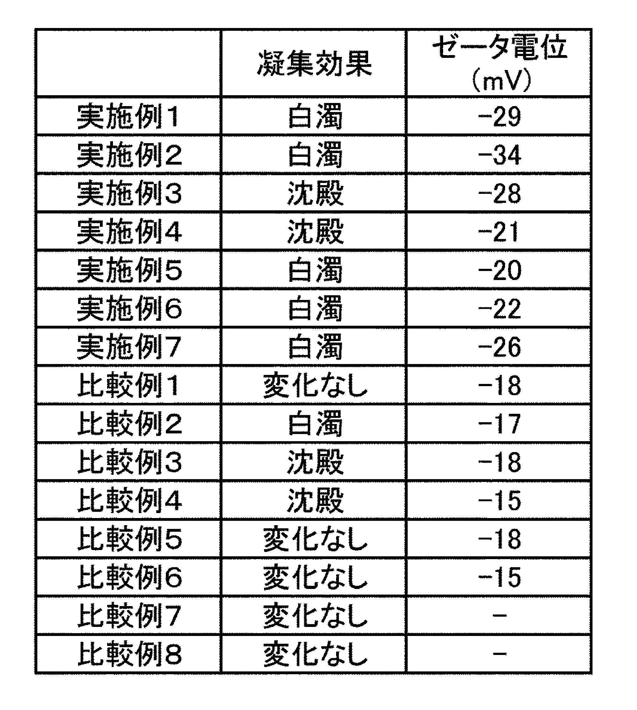
表2において、ゼータ電位(単位:mV)は、基板と洗浄の際に基板から離れた粒子との反発力の指標であり、マイナスの絶対値が大きいほど、反発力が大きくなることを示す。
-30mV未満:反発力が極めて大きい。
-30mV以上-20mV未満:反発力が大きく粒子の再付着が防止できる。
-20mV以上:成分(C)の効果が発揮されていない。
-30mV未満:反発力が極めて大きい。
-30mV以上-20mV未満:反発力が大きく粒子の再付着が防止できる。
-20mV以上:成分(C)の効果が発揮されていない。
本発明を詳細にまた特定の実施態様を参照して説明したが、本発明の精神と範囲を逸脱することなく様々な変更や修正を加えることができることは当業者にとって明らかである。本出願は2010年10月1日出願の日本特許出願(特願2010-224124)に基づくものであり、その内容はここに参照として取り込まれる。
本発明の半導体デバイス用基板洗浄液は、半導体デバイス用基板表面を腐食することなく、基板に付着した微粒子や有機汚染、金属汚染を同時に除去することが可能であり、水リンス性も良好であることから、本発明は半導体デバイスやディスプレイデバイスなどの製造工程における汚染半導体デバイス用基板の洗浄処理技術として、工業的に非常に有用である。
Claims (10)
- 半導体デバイス製造における化学的機械的研磨工程の後に行われる、半導体デバイス用基板の洗浄工程に用いられる洗浄液であって、以下の成分(A)~(D)を含有する半導体デバイス用基板洗浄液。
(A)有機酸
(B)スルホン酸型アニオン性界面活性剤
(C)ポリビニルピロリドン及びポリエチレンオキシド-ポリプロピレンオキシドブロック共重合体から選ばれる少なくとも1種の高分子凝集剤
(D)水 - 成分(A)が、カルボキシル基を1以上有する炭素数1~10の有機酸である請求項1記載の半導体デバイス用基板洗浄液。
- 成分(A)が、シュウ酸、クエン酸、酒石酸、リンゴ酸、乳酸、アスコルビン酸、没食子酸及び酢酸からなる群から選ばれた少なくとも1種である請求項2記載の半導体デバイス用基板洗浄液。
- 成分(B)が、アルキルスルホン酸及びその塩、アルキルベンゼンスルホン酸及びその塩、アルキルジフェニルエーテルジスルホン酸及びその塩、アルキルメチルタウリン酸及びその塩、並びにスルホコハク酸ジエステル及びその塩からなる群から選ばれた少なくとも1種である請求項1から3のいずれか1項に記載の半導体デバイス用基板洗浄液。
- 成分(A)が、5~30質量%、成分(B)が、0.01~10質量%、成分(C)が、0.001~10質量%の濃度で含有される請求項1から4のいずれか1項に記載の半導体デバイス用基板洗浄液。
- 成分(C)がポリビニルピロリドンであり、成分(A)が、0.03~3質量%、成分(B)が、0.0001~1質量%、成分(C)が、0.00001~0.003質量%の濃度で含有される請求項1~4のいずれか1項に記載の半導体デバイス用基板洗浄液。
- 成分(C)がポリエチレンオキシド-ポリプロピレンオキシドブロック共重合体であり、成分(A)が、0.03~3質量%、成分(B)が、0.0001~1質量%、成分(C)が、0.00001~0.03質量%の濃度で含有される請求項1~4のいずれか1項に記載の半導体デバイス用基板洗浄液。
- 水/洗浄液の質量比率を40とした調製液中で測定した、一次粒径が80nmのコロイダルシリカのゼータ電位が、-20mV以下である請求項1~4、6及び7のいずれか1項に記載の半導体デバイス用基板洗浄液。
- 請求項1から4及び6~8のいずれか1項に記載の半導体デバイス用基板洗浄液を用いて、半導体デバイス用基板を洗浄する半導体デバイス用基板の洗浄方法。
- 前記半導体デバイス用基板が、基板表面にCu配線と低誘電率絶縁膜を有し、かつ、化学的機械的研磨を行った後の前記半導体デバイス用基板を洗浄する請求項9に記載の半導体デバイス用基板の洗浄方法。
Priority Applications (2)
| Application Number | Priority Date | Filing Date | Title |
|---|---|---|---|
| KR1020137007595A KR101846597B1 (ko) | 2010-10-01 | 2011-09-29 | 반도체 디바이스용 기판의 세정액 및 세정 방법 |
| US13/854,235 US20130225464A1 (en) | 2010-10-01 | 2013-04-01 | Cleaning liquid for semiconductor device substrates and cleaning method |
Applications Claiming Priority (2)
| Application Number | Priority Date | Filing Date | Title |
|---|---|---|---|
| JP2010224124 | 2010-10-01 | ||
| JP2010-224124 | 2010-10-01 |
Related Child Applications (1)
| Application Number | Title | Priority Date | Filing Date |
|---|---|---|---|
| US13/854,235 Continuation US20130225464A1 (en) | 2010-10-01 | 2013-04-01 | Cleaning liquid for semiconductor device substrates and cleaning method |
Publications (1)
| Publication Number | Publication Date |
|---|---|
| WO2012043767A1 true WO2012043767A1 (ja) | 2012-04-05 |
Family
ID=45893204
Family Applications (1)
| Application Number | Title | Priority Date | Filing Date |
|---|---|---|---|
| PCT/JP2011/072466 Ceased WO2012043767A1 (ja) | 2010-10-01 | 2011-09-29 | 半導体デバイス用基板の洗浄液及び洗浄方法 |
Country Status (5)
| Country | Link |
|---|---|
| US (1) | US20130225464A1 (ja) |
| JP (1) | JP6014985B2 (ja) |
| KR (1) | KR101846597B1 (ja) |
| TW (1) | TW201215672A (ja) |
| WO (1) | WO2012043767A1 (ja) |
Cited By (4)
| Publication number | Priority date | Publication date | Assignee | Title |
|---|---|---|---|---|
| WO2018061365A1 (ja) * | 2016-09-28 | 2018-04-05 | 株式会社フジミインコーポレーテッド | 表面処理組成物 |
| JP2019502803A (ja) * | 2015-12-22 | 2019-01-31 | ビーエーエスエフ ソシエタス・ヨーロピアBasf Se | 化学機械研磨後の洗浄組成物 |
| CN114653665A (zh) * | 2022-02-14 | 2022-06-24 | 浙江富芯微电子科技有限公司 | 一种在碳化硅衬底化学抛光后清洗的方法 |
| TWI810765B (zh) * | 2021-01-07 | 2023-08-01 | 韓商细美事有限公司 | 處理液供應裝置以及處理液供應裝置的固體去除方法 |
Families Citing this family (12)
| Publication number | Priority date | Publication date | Assignee | Title |
|---|---|---|---|---|
| JP6123335B2 (ja) | 2012-02-17 | 2017-05-10 | 三菱化学株式会社 | 半導体デバイス用洗浄液及び半導体デバイス用基板の洗浄方法 |
| KR102628568B1 (ko) | 2015-07-16 | 2024-01-23 | 바스프 에스이 | 설포에스테르의 암모늄 염을 함유하는 결함 감소 헹굼 용액 |
| JP6880047B2 (ja) * | 2016-09-21 | 2021-06-02 | 株式会社フジミインコーポレーテッド | 表面処理組成物 |
| JP7061862B2 (ja) | 2016-10-28 | 2022-05-02 | 花王株式会社 | シリコンウェーハ用リンス剤組成物 |
| WO2018079675A1 (ja) | 2016-10-28 | 2018-05-03 | 花王株式会社 | シリコンウェーハ用リンス剤組成物 |
| KR102434647B1 (ko) * | 2017-01-17 | 2022-08-22 | 주식회사 다이셀 | 반도체 기판 세정제 |
| WO2018180256A1 (ja) * | 2017-03-31 | 2018-10-04 | 関東化學株式会社 | 洗浄液組成物 |
| SG11202004420QA (en) * | 2018-01-25 | 2020-06-29 | Merck Patent Gmbh | Photoresist remover compositions |
| US11560533B2 (en) * | 2018-06-26 | 2023-01-24 | Versum Materials Us, Llc | Post chemical mechanical planarization (CMP) cleaning |
| JP7230621B2 (ja) * | 2019-03-25 | 2023-03-01 | 三菱ケミカル株式会社 | 半導体ウェハの洗浄方法及び半導体ウェハの製造方法 |
| KR20250054080A (ko) | 2022-09-30 | 2025-04-22 | 후지필름 가부시키가이샤 | 조성물, 기판의 처리 방법, 반도체 디바이스의 제조 방법, 화합물 |
| WO2024190141A1 (ja) | 2023-03-15 | 2024-09-19 | 富士フイルム株式会社 | 処理液、被処理物の洗浄方法、電子デバイスの製造方法 |
Citations (1)
| Publication number | Priority date | Publication date | Assignee | Title |
|---|---|---|---|---|
| JP2008047842A (ja) * | 2006-08-21 | 2008-02-28 | Jsr Corp | 洗浄用組成物、洗浄方法及び半導体装置の製造方法 |
Family Cites Families (16)
| Publication number | Priority date | Publication date | Assignee | Title |
|---|---|---|---|---|
| JPH1143791A (ja) * | 1997-07-23 | 1999-02-16 | Mitsubishi Chem Corp | 研磨液用洗浄剤組成物 |
| JP2001252630A (ja) * | 2000-03-10 | 2001-09-18 | Sharp Corp | 洗浄方法 |
| DE60124473T2 (de) * | 2000-09-08 | 2007-09-06 | Kanto Kagaku K.K. | Ätzflüssigkeitszusammensetzung |
| EP1389496A1 (en) | 2001-05-22 | 2004-02-18 | Mitsubishi Chemical Corporation | Method for cleaning surface of substrate |
| JP2003068696A (ja) | 2001-05-22 | 2003-03-07 | Mitsubishi Chemicals Corp | 基板表面洗浄方法 |
| TWI302950B (en) * | 2002-01-28 | 2008-11-11 | Mitsubishi Chem Corp | Cleaning solution and method of cleanimg board of semiconductor device |
| DE602005000732T2 (de) * | 2004-06-25 | 2007-12-06 | Jsr Corp. | Reinigungszusammensetzung für Halbleiterkomponente und Verfahren zur Herstellung eines Halbleitergeräts |
| JP4804986B2 (ja) * | 2006-03-30 | 2011-11-02 | 富士フイルム株式会社 | 半導体デバイス用基板の洗浄液及びそれを用いた洗浄方法 |
| US9058975B2 (en) * | 2006-06-09 | 2015-06-16 | Lam Research Corporation | Cleaning solution formulations for substrates |
| US20100273330A1 (en) * | 2006-08-23 | 2010-10-28 | Citibank N.A. As Collateral Agent | Rinse formulation for use in the manufacture of an integrated circuit |
| US20080125342A1 (en) * | 2006-11-07 | 2008-05-29 | Advanced Technology Materials, Inc. | Formulations for cleaning memory device structures |
| US20090056744A1 (en) * | 2007-08-29 | 2009-03-05 | Micron Technology, Inc. | Wafer cleaning compositions and methods |
| US8226775B2 (en) * | 2007-12-14 | 2012-07-24 | Lam Research Corporation | Methods for particle removal by single-phase and two-phase media |
| JP5813280B2 (ja) * | 2008-03-19 | 2015-11-17 | 富士フイルム株式会社 | 半導体デバイス用洗浄液、および洗浄方法 |
| US8227394B2 (en) * | 2008-11-07 | 2012-07-24 | Lam Research Corporation | Composition of a cleaning material for particle removal |
| JP5455452B2 (ja) * | 2009-06-05 | 2014-03-26 | Jsr株式会社 | 表面処理用組成物、表面処理方法および半導体装置の製造方法 |
-
2011
- 2011-09-29 KR KR1020137007595A patent/KR101846597B1/ko active Active
- 2011-09-29 WO PCT/JP2011/072466 patent/WO2012043767A1/ja not_active Ceased
- 2011-09-29 JP JP2011214851A patent/JP6014985B2/ja active Active
- 2011-09-30 TW TW100135815A patent/TW201215672A/zh unknown
-
2013
- 2013-04-01 US US13/854,235 patent/US20130225464A1/en not_active Abandoned
Patent Citations (1)
| Publication number | Priority date | Publication date | Assignee | Title |
|---|---|---|---|---|
| JP2008047842A (ja) * | 2006-08-21 | 2008-02-28 | Jsr Corp | 洗浄用組成物、洗浄方法及び半導体装置の製造方法 |
Cited By (7)
| Publication number | Priority date | Publication date | Assignee | Title |
|---|---|---|---|---|
| JP2019502803A (ja) * | 2015-12-22 | 2019-01-31 | ビーエーエスエフ ソシエタス・ヨーロピアBasf Se | 化学機械研磨後の洗浄組成物 |
| WO2018061365A1 (ja) * | 2016-09-28 | 2018-04-05 | 株式会社フジミインコーポレーテッド | 表面処理組成物 |
| JPWO2018061365A1 (ja) * | 2016-09-28 | 2019-07-18 | 株式会社フジミインコーポレーテッド | 表面処理組成物 |
| JP7028782B2 (ja) | 2016-09-28 | 2022-03-02 | 株式会社フジミインコーポレーテッド | 表面処理組成物 |
| TWI810765B (zh) * | 2021-01-07 | 2023-08-01 | 韓商细美事有限公司 | 處理液供應裝置以及處理液供應裝置的固體去除方法 |
| US12322610B2 (en) | 2021-01-07 | 2025-06-03 | Semes Co., Ltd. | Processing liquid supply apparatus and method of removing solids from processing liquid supply apparatus |
| CN114653665A (zh) * | 2022-02-14 | 2022-06-24 | 浙江富芯微电子科技有限公司 | 一种在碳化硅衬底化学抛光后清洗的方法 |
Also Published As
| Publication number | Publication date |
|---|---|
| KR20130115228A (ko) | 2013-10-21 |
| US20130225464A1 (en) | 2013-08-29 |
| JP6014985B2 (ja) | 2016-10-26 |
| TW201215672A (en) | 2012-04-16 |
| KR101846597B1 (ko) | 2018-04-06 |
| JP2012094852A (ja) | 2012-05-17 |
Similar Documents
| Publication | Publication Date | Title |
|---|---|---|
| JP6014985B2 (ja) | 半導体デバイス用基板洗浄液及び洗浄方法 | |
| JP5948758B2 (ja) | 半導体デバイス用基板洗浄液及び洗浄方法 | |
| JP6123334B2 (ja) | 半導体デバイス用洗浄液及び半導体デバイス用基板の洗浄方法 | |
| JP6711437B2 (ja) | 半導体デバイス用基板洗浄液及び半導体デバイス用基板の洗浄方法 | |
| JP6488740B2 (ja) | 半導体デバイス用基板洗浄液及び半導体デバイス用基板の洗浄方法 | |
| TWI736567B (zh) | 用於化學機械硏磨後清潔之組成物 | |
| TWI648430B (zh) | 半導體裝置用基板洗淨液及半導體裝置用基板之洗淨方法 | |
| TWI745569B (zh) | 半導體裝置用基板之清潔液、半導體裝置用基板之清潔方法、半導體裝置用基板之製造方法及半導體裝置用基板 | |
| KR20200058428A (ko) | 세정액, 세정 방법 및 반도체 웨이퍼의 제조 방법 | |
| CN108473918A (zh) | 用于化学机械抛光后清洁的组合物 | |
| JP2014036136A (ja) | 半導体デバイス用基板洗浄液及び半導体デバイス用基板の洗浄方法 | |
| TW201903138A (zh) | 半導體裝置用基板之清潔劑組合物、半導體裝置用基板之清潔方法、半導體裝置用基板之製造方法及半導體裝置用基板 | |
| JP5817310B2 (ja) | 半導体デバイス用基板の洗浄液及び洗浄方法 | |
| KR20190016093A (ko) | 포스트 화학적-기계적-폴리싱 세정용 조성물 | |
| JP2014154625A (ja) | 半導体デバイス用基板の洗浄液及び洗浄方法 | |
| JP6635213B2 (ja) | 半導体デバイス用基板洗浄液及び半導体デバイス用基板の洗浄方法 | |
| JP2015203047A (ja) | 半導体デバイス用基板洗浄液及び半導体デバイス用基板の洗浄方法 | |
| JP2012119513A (ja) | 半導体デバイス用基板洗浄液及び洗浄方法 | |
| JP2016178118A (ja) | 半導体デバイス用基板洗浄液及び半導体デバイス用基板の洗浄方法 |
Legal Events
| Date | Code | Title | Description |
|---|---|---|---|
| 121 | Ep: the epo has been informed by wipo that ep was designated in this application |
Ref document number: 11829320 Country of ref document: EP Kind code of ref document: A1 |
|
| ENP | Entry into the national phase |
Ref document number: 20137007595 Country of ref document: KR Kind code of ref document: A |
|
| NENP | Non-entry into the national phase |
Ref country code: DE |
|
| 122 | Ep: pct application non-entry in european phase |
Ref document number: 11829320 Country of ref document: EP Kind code of ref document: A1 |