WO2011125277A1 - 放射線検出器およびそれを製造する方法 - Google Patents
放射線検出器およびそれを製造する方法 Download PDFInfo
- Publication number
- WO2011125277A1 WO2011125277A1 PCT/JP2011/000953 JP2011000953W WO2011125277A1 WO 2011125277 A1 WO2011125277 A1 WO 2011125277A1 JP 2011000953 W JP2011000953 W JP 2011000953W WO 2011125277 A1 WO2011125277 A1 WO 2011125277A1
- Authority
- WO
- WIPO (PCT)
- Prior art keywords
- substrate
- semiconductor layer
- radiation detector
- radiation
- blocking layer
- Prior art date
Links
- 230000005855 radiation Effects 0.000 title claims abstract description 107
- 238000004519 manufacturing process Methods 0.000 title claims description 28
- 239000000758 substrate Substances 0.000 claims abstract description 329
- 239000004065 semiconductor Substances 0.000 claims abstract description 166
- OKTJSMMVPCPJKN-UHFFFAOYSA-N Carbon Chemical compound [C] OKTJSMMVPCPJKN-UHFFFAOYSA-N 0.000 claims abstract description 130
- 229910002804 graphite Inorganic materials 0.000 claims abstract description 129
- 239000010439 graphite Substances 0.000 claims abstract description 129
- 230000000903 blocking effect Effects 0.000 claims abstract description 96
- 238000000034 method Methods 0.000 claims description 31
- 229910007709 ZnTe Inorganic materials 0.000 claims description 23
- 229910004613 CdTe Inorganic materials 0.000 claims description 22
- 229910004611 CdZnTe Inorganic materials 0.000 claims description 22
- 238000004381 surface treatment Methods 0.000 claims description 20
- 238000004140 cleaning Methods 0.000 claims description 18
- 239000000463 material Substances 0.000 claims description 15
- 238000005422 blasting Methods 0.000 claims description 12
- 238000005498 polishing Methods 0.000 claims description 12
- SKJCKYVIQGBWTN-UHFFFAOYSA-N (4-hydroxyphenyl) methanesulfonate Chemical compound CS(=O)(=O)OC1=CC=C(O)C=C1 SKJCKYVIQGBWTN-UHFFFAOYSA-N 0.000 claims description 11
- MARUHZGHZWCEQU-UHFFFAOYSA-N 5-phenyl-2h-tetrazole Chemical compound C1=CC=CC=C1C1=NNN=N1 MARUHZGHZWCEQU-UHFFFAOYSA-N 0.000 claims description 11
- QWUZMTJBRUASOW-UHFFFAOYSA-N cadmium tellanylidenezinc Chemical compound [Zn].[Cd].[Te] QWUZMTJBRUASOW-UHFFFAOYSA-N 0.000 claims description 11
- 238000005530 etching Methods 0.000 claims description 11
- 238000003801 milling Methods 0.000 claims description 11
- VYPSYNLAJGMNEJ-UHFFFAOYSA-N Silicium dioxide Chemical compound O=[Si]=O VYPSYNLAJGMNEJ-UHFFFAOYSA-N 0.000 claims description 7
- 238000010304 firing Methods 0.000 claims description 7
- 229910052582 BN Inorganic materials 0.000 claims description 6
- PZNSFCLAULLKQX-UHFFFAOYSA-N Boron nitride Chemical compound N#B PZNSFCLAULLKQX-UHFFFAOYSA-N 0.000 claims description 6
- 229910052581 Si3N4 Inorganic materials 0.000 claims description 6
- PMHQVHHXPFUNSP-UHFFFAOYSA-M copper(1+);methylsulfanylmethane;bromide Chemical compound Br[Cu].CSC PMHQVHHXPFUNSP-UHFFFAOYSA-M 0.000 claims description 6
- 239000000203 mixture Substances 0.000 claims description 6
- TWNQGVIAIRXVLR-UHFFFAOYSA-N oxo(oxoalumanyloxy)alumane Chemical compound O=[Al]O[Al]=O TWNQGVIAIRXVLR-UHFFFAOYSA-N 0.000 claims description 6
- HBMJWWWQQXIZIP-UHFFFAOYSA-N silicon carbide Chemical compound [Si+]#[C-] HBMJWWWQQXIZIP-UHFFFAOYSA-N 0.000 claims description 6
- 229910010271 silicon carbide Inorganic materials 0.000 claims description 6
- HQVNEWCFYHHQES-UHFFFAOYSA-N silicon nitride Chemical compound N12[Si]34N5[Si]62N3[Si]51N64 HQVNEWCFYHHQES-UHFFFAOYSA-N 0.000 claims description 6
- 229910052814 silicon oxide Inorganic materials 0.000 claims description 6
- 238000010030 laminating Methods 0.000 claims description 5
- 230000000694 effects Effects 0.000 abstract description 11
- 239000010408 film Substances 0.000 description 25
- 239000003990 capacitor Substances 0.000 description 20
- 239000010409 thin film Substances 0.000 description 12
- 238000010586 diagram Methods 0.000 description 8
- 239000012535 impurity Substances 0.000 description 5
- 239000002245 particle Substances 0.000 description 5
- 239000004020 conductor Substances 0.000 description 4
- 238000005092 sublimation method Methods 0.000 description 4
- 230000003746 surface roughness Effects 0.000 description 4
- 230000015572 biosynthetic process Effects 0.000 description 3
- 239000011521 glass Substances 0.000 description 3
- 238000004544 sputter deposition Methods 0.000 description 3
- 238000007740 vapor deposition Methods 0.000 description 3
- CURLTUGMZLYLDI-UHFFFAOYSA-N Carbon dioxide Chemical compound O=C=O CURLTUGMZLYLDI-UHFFFAOYSA-N 0.000 description 2
- -1 ITO Substances 0.000 description 2
- 238000009388 chemical precipitation Methods 0.000 description 2
- 239000013078 crystal Substances 0.000 description 2
- 238000004070 electrodeposition Methods 0.000 description 2
- 229910052737 gold Inorganic materials 0.000 description 2
- 238000003475 lamination Methods 0.000 description 2
- 230000002093 peripheral effect Effects 0.000 description 2
- 238000012545 processing Methods 0.000 description 2
- 238000012546 transfer Methods 0.000 description 2
- 239000011701 zinc Substances 0.000 description 2
- 229910018072 Al 2 O 3 Inorganic materials 0.000 description 1
- 235000010627 Phaseolus vulgaris Nutrition 0.000 description 1
- 244000046052 Phaseolus vulgaris Species 0.000 description 1
- 238000010521 absorption reaction Methods 0.000 description 1
- 230000002411 adverse Effects 0.000 description 1
- PNEYBMLMFCGWSK-UHFFFAOYSA-N aluminium oxide Inorganic materials [O-2].[O-2].[O-2].[Al+3].[Al+3] PNEYBMLMFCGWSK-UHFFFAOYSA-N 0.000 description 1
- 230000004888 barrier function Effects 0.000 description 1
- 229910052799 carbon Inorganic materials 0.000 description 1
- 229910002092 carbon dioxide Inorganic materials 0.000 description 1
- 239000001569 carbon dioxide Substances 0.000 description 1
- 238000006243 chemical reaction Methods 0.000 description 1
- 238000005520 cutting process Methods 0.000 description 1
- 238000000151 deposition Methods 0.000 description 1
- 238000002474 experimental method Methods 0.000 description 1
- 238000002488 metal-organic chemical vapour deposition Methods 0.000 description 1
- 239000000843 powder Substances 0.000 description 1
- 238000011160 research Methods 0.000 description 1
- 239000004576 sand Substances 0.000 description 1
- 238000005488 sandblasting Methods 0.000 description 1
- 229910052710 silicon Inorganic materials 0.000 description 1
- 239000010703 silicon Substances 0.000 description 1
- 238000009751 slip forming Methods 0.000 description 1
- 238000005507 spraying Methods 0.000 description 1
- 230000000087 stabilizing effect Effects 0.000 description 1
- 238000003860 storage Methods 0.000 description 1
- 238000000859 sublimation Methods 0.000 description 1
- 230000008022 sublimation Effects 0.000 description 1
- JBQYATWDVHIOAR-UHFFFAOYSA-N tellanylidenegermanium Chemical compound [Te]=[Ge] JBQYATWDVHIOAR-UHFFFAOYSA-N 0.000 description 1
- 238000013518 transcription Methods 0.000 description 1
- 230000035897 transcription Effects 0.000 description 1
Images


Classifications
-
- H—ELECTRICITY
- H01—ELECTRIC ELEMENTS
- H01L—SEMICONDUCTOR DEVICES NOT COVERED BY CLASS H10
- H01L31/00—Semiconductor devices sensitive to infrared radiation, light, electromagnetic radiation of shorter wavelength or corpuscular radiation and specially adapted either for the conversion of the energy of such radiation into electrical energy or for the control of electrical energy by such radiation; Processes or apparatus specially adapted for the manufacture or treatment thereof or of parts thereof; Details thereof
- H01L31/02—Details
- H01L31/0236—Special surface textures
-
- H—ELECTRICITY
- H01—ELECTRIC ELEMENTS
- H01L—SEMICONDUCTOR DEVICES NOT COVERED BY CLASS H10
- H01L27/00—Devices consisting of a plurality of semiconductor or other solid-state components formed in or on a common substrate
- H01L27/14—Devices consisting of a plurality of semiconductor or other solid-state components formed in or on a common substrate including semiconductor components sensitive to infrared radiation, light, electromagnetic radiation of shorter wavelength or corpuscular radiation and specially adapted either for the conversion of the energy of such radiation into electrical energy or for the control of electrical energy by such radiation
- H01L27/144—Devices controlled by radiation
- H01L27/146—Imager structures
- H01L27/14601—Structural or functional details thereof
- H01L27/14636—Interconnect structures
-
- Y—GENERAL TAGGING OF NEW TECHNOLOGICAL DEVELOPMENTS; GENERAL TAGGING OF CROSS-SECTIONAL TECHNOLOGIES SPANNING OVER SEVERAL SECTIONS OF THE IPC; TECHNICAL SUBJECTS COVERED BY FORMER USPC CROSS-REFERENCE ART COLLECTIONS [XRACs] AND DIGESTS
- Y02—TECHNOLOGIES OR APPLICATIONS FOR MITIGATION OR ADAPTATION AGAINST CLIMATE CHANGE
- Y02E—REDUCTION OF GREENHOUSE GAS [GHG] EMISSIONS, RELATED TO ENERGY GENERATION, TRANSMISSION OR DISTRIBUTION
- Y02E10/00—Energy generation through renewable energy sources
- Y02E10/50—Photovoltaic [PV] energy
Definitions
- the present invention relates to a radiation detector used in the medical field, the industrial field, the nuclear field, and the like, and a method of manufacturing the same.
- CdTe cadmium telluride
- ZnTe zinc telluride
- CdZnTe cadmium zinc telluride
- the present invention has been made in view of such circumstances, and a radiation detector capable of stabilizing the film quality of a semiconductor layer formed on a substrate and improving the adhesion between the substrate and the semiconductor layer. It is an object to provide a method for manufacturing the same.
- the state of the substrate surface on which the semiconductor layers are stacked is not defined, and it has been unclear what kind of problem occurs depending on the state of the substrate surface. Therefore, focusing on the substrate, it has been found through experiments that the surface roughness of the substrate affects the semiconductor layer.
- the experimental data shown in FIGS. 5 (a) to 5 (c) when a graphite substrate is used as the substrate shows that if the irregularities are large, the crystal growth of the stacked semiconductor layer will be adversely affected, and leakage may occur. If spots are generated and the concavities and convexities are small, the adhesion of the semiconductor layers formed by lamination is poor, and a porous film quality is formed.
- FIG. 5 (a) shows an image observed at x100 magnification by laminating (depositing) a semiconductor layer on a substrate with irregularities (surface roughness) in the range of 1 ⁇ m to 8 ⁇ m.
- FIG. 5B shows an image of ⁇ 100 magnification obtained by forming a semiconductor layer on a substrate having the unevenness of less than 1 ⁇ m
- FIG. 5C shows an image of forming the semiconductor layer on a substrate having the unevenness exceeding 8 ⁇ m.
- a 500 ⁇ image is shown.
- the film forming conditions other than the substrate are all the same, and the difference due to only the surface difference is seen from the image. As can be seen from FIG.
- FIG. 5 (b) it can be seen that the semiconductor layer laminated on the substrate having the unevenness of less than 1 ⁇ m is coarse and porous as compared with FIG. 5 (a).
- FIG. 5C it can be seen that the semiconductor layer laminated on the substrate with the unevenness exceeding 8 ⁇ m has a boundary of the film quality of the semiconductor layer from the upper left to the lower right on the image. Such a boundary is dotted on a substrate having irregularities exceeding 8 ⁇ m, and a leak spot portion where excessive leakage current flows is formed at that portion.
- the radiation detector according to the present invention is a radiation detector for detecting radiation, which converts radiation information into charge information by the incidence of radiation, CdTe (cadmium telluride), ZnTe (zinc telluride) or A polycrystalline semiconductor layer formed of CdZnTe (cadmium zinc telluride), a bias voltage is applied to the semiconductor layer, a graphite substrate for a voltage application electrode also serving as a support substrate, the charge information is read, and the pixel And a readout substrate having a pixel electrode formed in accordance with each, the semiconductor layer is laminated on the graphite substrate, and the semiconductor layer is laminated so that the semiconductor layer and the pixel electrode are bonded to each other inside When the formed graphite substrate and the readout substrate are bonded together to form each, the graphite substrate Unevenness of the surface is characterized in that in the range of 1 [mu] m ⁇ 8 [mu] m.
- a polycrystalline semiconductor layer formed of CdTe, ZnTe, or CdZnTe is used, and a graphite substrate serving as both a voltage application electrode and a support substrate is used as a substrate.
- the irregularities on the surface of the graphite substrate are in the range of 1 ⁇ m to 8 ⁇ m. By setting it within this range, it is possible to prevent the substrate layer having irregularities of less than 1 ⁇ m from being rough and porous, resulting in poor adhesion between the substrate and the semiconductor layer, and conversely, substrates having irregularities exceeding 8 ⁇ m. Let's prevent leak spots. As a result, the film quality of the semiconductor layer stacked on the substrate is stabilized, and the adhesion between the substrate and the semiconductor layer can be improved.
- a radiation detector different from the above-described radiation detector is a radiation detector that detects radiation, and converts radiation information into charge information by the incidence of radiation, and CdTe (cadmium telluride), ZnTe ( A polycrystalline semiconductor layer formed of zinc telluride) or CdZnTe (cadmium zinc telluride), a bias voltage is applied to the semiconductor layer, and a graphite substrate for a voltage application electrode also serving as a support substrate; A pixel electrode formed in accordance with each pixel for reading out information and a readout substrate on which a readout pattern is formed are provided, the semiconductor layer is laminated on the graphite substrate, and the pixel electrode is laminated on the semiconductor layer And a graphite layer in which a semiconductor layer is laminated with the pixel electrode so that the pixel electrode is bonded to the readout substrate side.
- CdTe cadmium telluride
- ZnTe A polycrystalline semiconductor layer formed of zinc telluride
- CdZnTe cadmium zinc
- a polycrystalline semiconductor layer formed of CdTe, ZnTe, or CdZnTe is used, and a graphite substrate serving as both a voltage application electrode and a support substrate is used as a substrate.
- the irregularities on the surface of the graphite substrate are in the range of 1 ⁇ m to 8 ⁇ m. By setting it within this range, it is possible to prevent the substrate layer having irregularities of less than 1 ⁇ m from being rough and porous, resulting in poor adhesion between the substrate and the semiconductor layer, and conversely, substrates having irregularities exceeding 8 ⁇ m. Let's prevent leak spots. As a result, the film quality of the semiconductor layer stacked on the substrate is stabilized, and the adhesion between the substrate and the semiconductor layer can be improved.
- another radiation detector other than the above-described radiation detector is a radiation detector that detects radiation, and converts radiation information into charge information by the incidence of radiation, so that CdTe (cadmium telluride), ZnTe (Zinc Telluride) or CdZnTe (Cadmium Zinc Telluride), a polycrystalline semiconductor layer, a voltage application electrode for applying a bias voltage to the semiconductor layer, and reading out the charge information, depending on the pixel
- the formed pixel electrode, the voltage application electrode, the semiconductor layer, and the pixel electrode are supported, and are formed of any of aluminum oxide, aluminum nitride, boron nitride, silicon oxide, silicon nitride, or silicon carbide, or these materials
- the voltage application electrode is stacked on the support substrate, the semiconductor layer is stacked on the voltage application electrode, the pixel electrode is stacked on the semiconductor layer, and the pixel electrode is
- the unevenness of the surface of the support substrate is in the range of 1 ⁇ m to 8 ⁇ m. It is characterized by this.
- a semiconductor substrate of a polycrystalline film formed of CdTe, ZnTe or CdZnTe, which is supported as a substrate independently of a voltage application electrode, is provided.
- the unevenness of the surface of the support substrate is set in the range of 1 ⁇ m to 8 ⁇ m. By setting it within this range, it is possible to prevent the substrate layer having irregularities of less than 1 ⁇ m from being rough and porous, resulting in poor adhesion between the substrate and the semiconductor layer, and conversely, substrates having irregularities exceeding 8 ⁇ m. Let's prevent leak spots.
- the film quality of the semiconductor layer stacked on the substrate is stabilized, and the adhesion between the substrate and the semiconductor layer can be improved.
- the support substrate is formed of any of aluminum oxide, aluminum nitride, boron nitride, silicon oxide, silicon nitride, or silicon carbide, or formed by firing a mixture of these materials. It only has to be done.
- the voltage application electrode is interposed between the support substrate and the semiconductor layer, but the voltage application electrode is thin, and the unevenness on the surface of the support substrate is transferred to the voltage application electrode, so that the unevenness on the surface of the support substrate is 1 ⁇ m.
- the thickness is in the range of ⁇ 8 ⁇ m, the irregularities on the surface of the voltage application electrode are also in the range, and the effect is almost the same as the structure in which the semiconductor layer is formed on the support substrate.
- the electron blocking layer and the hole blocking layer is formed in direct contact with the semiconductor layer.
- the blocking layer is thin, and irregularities on the surface of the graphite substrate or the supporting substrate are transferred to the blocking layer. Therefore, if the unevenness of the surface of the graphite substrate or the support substrate is in the range of 1 ⁇ m to 8 ⁇ m, the unevenness of the surface of the blocking layer is also almost in this range, and the structure is formed by directly contacting the semiconductor layer with the graphite substrate or the support substrate. Has almost the same effect.
- the surface of the substrate is subjected to surface treatment using any one of milling, polishing, blasting, or etching for the irregularities on the surface of the substrate.
- the unevenness of the surface of the substrate is in the range of 1 ⁇ m to 8 ⁇ m, so that the semiconductor layer stacked on the substrate can be formed.
- the film quality is stable and the adhesion between the substrate and the semiconductor layer can be improved.
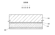
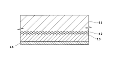
- FIG. 3 is a longitudinal sectional view showing a configuration of a radiation detector according to Example 1 on a graphite substrate side.
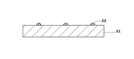
- FIG. FIG. 3 is a longitudinal sectional view showing a configuration on the readout substrate side of the radiation detector according to the first embodiment. It is a circuit diagram which shows the structure of a read-out board
- the experimental data when a graphite substrate is used as the substrate (a) is an image obtained by forming a semiconductor layer on the substrate with surface irregularities in the range of 1 ⁇ m to 8 ⁇ m and observing it at ⁇ 100 magnification, (b ) Is a ⁇ 100 magnification image obtained by forming a semiconductor layer on a substrate having the unevenness of less than 1 ⁇ m, and (c) is a ⁇ 500 magnification image obtained by forming a semiconductor layer on the substrate having the unevenness exceeding 8 ⁇ m.
- FIG. 1 It is a longitudinal cross-sectional view when the structure by the side of a graphite substrate and the structure by the side of a reading substrate are bonded together in the radiation detector which concerns on Example 2.
- FIG. It is a longitudinal cross-sectional view when the structure by the side of a support substrate and the structure by the side of a reading substrate are bonded together in the radiation detector which concerns on Example 3.
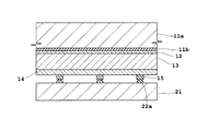
- FIG. It is a schematic diagram for explaining the transfer of irregularities when a voltage application electrode and an electron blocking layer are interposed between a support substrate and a semiconductor layer.
- FIG. 1 is a longitudinal sectional view showing the configuration of the radiation detector according to the first embodiment on the graphite substrate side
- FIG. 2 is a longitudinal sectional view showing the configuration of the radiation detector according to the first embodiment on the readout substrate side
- FIG. 3 is a circuit diagram showing the configuration of the readout substrate and the peripheral circuit
- FIG. 4 is a longitudinal sectional view when the configuration on the graphite substrate side and the configuration on the readout substrate side according to Example 1 are bonded together. It is.
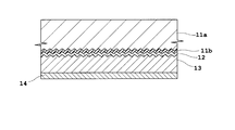
- the radiation detector is roughly divided into a graphite substrate 11 and a readout substrate 21 as shown in FIGS.
- an electron blocking layer 12, a semiconductor layer 13, and a hole blocking layer 14 are laminated on a graphite substrate 11 in this order.
- the readout substrate 21 has a pixel electrode 22 to be described later, and a capacitor 23, a thin film transistor 24, and the like are patterned (only the readout substrate 21 and the pixel electrode 22 are shown in FIG. 2).
- the graphite substrate 11 corresponds to the graphite substrate in this invention
- the electron blocking layer 12 corresponds to the electron blocking layer in this invention
- the semiconductor layer 13 corresponds to the semiconductor layer in this invention
- the hole blocking layer 14
- the readout substrate 21 corresponds to the readout substrate in the present invention
- the pixel electrode 22 corresponds to the pixel electrode in the present invention.
- the graphite substrate 11 serves both as a support substrate 11a and a voltage application electrode 11b in Example 3 described later. That is, a bias voltage (a bias voltage of ⁇ 0.1 V / ⁇ m to 1 V / ⁇ m in each of Examples 1 to 3) is applied to the semiconductor layer 13 and the graphite substrate 11 serving as a voltage application electrode also serving as the support substrate 11a is used.
- the radiation detector according to the first embodiment is constructed.
- the graphite substrate 11 is made of a conductive carbon graphite plate material, and uses a flat plate material (thickness of about 2 mm) whose firing conditions are adjusted in order to match the thermal expansion coefficient of the semiconductor layer 13.
- the semiconductor layer 13 converts radiation information into charge information (carrier) by the incidence of radiation (for example, X-rays).
- a polycrystalline film formed of CdTe (cadmium telluride), ZnTe (zinc telluride) or CdZnTe (cadmium zinc telluride) is used for the semiconductor layer 13.
- the thermal expansion coefficients of these semiconductor layers 13 are about 5 ppm / deg for CdTe and about 8 ppm / deg for ZnTe, and CdZnTe takes an intermediate value according to the Zn concentration.
- a P-type semiconductor such as ZnTe, Sb 2 S 3 , or Sb 2 Te 3 is used.
- an N-type such as CdS, ZnS, ZnO, or Sb 2 S 3 or Use ultra-high resistance semiconductors. 1 and 4, the hole blocking layer 14 is continuously formed. However, when the film resistance of the hole blocking layer 14 is low, the hole blocking layer 14 may be formed separately corresponding to the pixel electrode 22. When the hole blocking layer 14 is formed separately corresponding to the pixel electrode 22, the alignment of the hole blocking layer 14 and the pixel electrode 22 is performed when the graphite substrate 11 and the readout substrate 21 are bonded together. Is required. If there is no problem in the characteristics of the radiation detector, either or both of the electron blocking layer 12 and the hole blocking layer 14 may be omitted.
- the readout substrate 21 has a conductive material (conductive paste, anisotropic conductive film (ACF), anisotropic) at a location (pixel region) of a capacitance electrode 23 a (see FIG. 4) of the capacitor 23 described later.
- the pixel electrode 22 is formed in the place by bump connection at the time of bonding to the graphite substrate 11 with a conductive paste or the like. As described above, the pixel electrode 22 is formed according to each pixel, and reads the carrier converted by the semiconductor layer 13. As the reading substrate 21, a glass substrate is used.
- the readout substrate 21 has a pattern in which a capacitor 23 as a charge storage capacitor and a thin film transistor 24 as a switching element are divided for each pixel.
- a readout substrate 21 having a size (for example, 1024 ⁇ 1024 pixels) that matches the number of pixels of the two-dimensional radiation detector is used.
- the capacitor electrode 23 a of the capacitor 23 and the gate electrode 24 a of the thin film transistor 24 are stacked on the surface of the readout substrate 21 and covered with the insulating layer 25.
- a reference electrode 23b of the capacitor 23 is stacked on the insulating layer 25 so as to face the capacitor electrode 23a with the insulating layer 25 interposed therebetween, and a source electrode 24b and a drain electrode 24c of the thin film transistor 24 are stacked to form a pixel electrode.
- the insulating layer 26 is covered except for the connection portion 22. Note that the capacitor electrode 23a and the source electrode 24b are electrically connected to each other. As shown in FIG. 4, the capacitor electrode 23a and the source electrode 24b may be integrally formed simultaneously.
- the reference electrode 23b is grounded.
- plasma SiN is used for the insulating layers 25 and 26, for example, plasma SiN is used.
- the gate line 27 is electrically connected to the gate electrode 24a of the thin film transistor 24 shown in FIG. 4, and the data line 28 is electrically connected to the drain electrode 24c of the thin film transistor 24 shown in FIG. Yes.
- the gate line 27 extends in the row direction of each pixel, and the data line 28 extends in the column direction of each pixel.
- the gate line 27 and the data line 28 are orthogonal to each other.
- the capacitor 23, the thin film transistor 24, and the insulating layers 25 and 26 including the gate line 27 and the data line 28 are patterned on the surface of the reading substrate 21 made of a glass substrate using a semiconductor thin film manufacturing technique or a fine processing technique.
- a gate drive circuit 29 and a readout circuit 30 are provided around the readout substrate 21.
- the gate drive circuit 29 is electrically connected to the gate line 27 extending to each row, and sequentially drives the pixels in each row.
- the readout circuit 30 is electrically connected to the data line 28 extending in each column, and reads out the carrier of each pixel through the data line 28.
- the gate drive circuit 29 and the readout circuit 30 are composed of a semiconductor integrated circuit such as silicon, and electrically connect the gate line 27 and the data line 28 via an anisotropic conductive film (ACF) or the like.
- ACF anisotropic conductive film
- Surface treatment is performed so that the unevenness of the surface of the graphite substrate 11 is in the range of 1 ⁇ m to 8 ⁇ m.
- a cleaning process for cleaning the graphite substrate 11 is performed to remove impurities, particles, and the like on the surface of the graphite substrate 11.
- milling that performs cutting by applying rotation may be applied to the graphite substrate 11, or polishing may be applied to the graphite substrate 11.
- blasting may be performed by causing a powder such as carbon dioxide (CO 2 ), glass beans, or alumina (Al 2 O 3 ) to collide with the once flattened graphite substrate 11.
- an etching process may be applied to the graphite substrate 11.
- the surface unevenness of the graphite substrate 11 is subjected to surface treatment using any one of milling, polishing, blasting, or etching, so that the surface unevenness of the graphite substrate 11 is in the range of 1 ⁇ m to 8 ⁇ m. Process.
- an electron blocking layer 12 is formed on the graphite substrate 11 having a surface roughness of 1 ⁇ m to 8 ⁇ m by a sublimation method, a vapor deposition method, a sputtering method, a chemical precipitation method, an electrodeposition method, or the like.
- a semiconductor layer 13 which is a conversion layer is laminated on the electron blocking layer 12 by a sublimation method.
- a ZnTe or CdZnTe film containing zinc (Zn) having a thickness of about 300 ⁇ m and containing about several mol% to several tens mol% for use as an X-ray detector having an energy of several tens keV to several hundreds keV is a semiconductor layer. 13 is formed by proximity sublimation.
- a CdTe film containing no Zn may be formed as the semiconductor layer 13.
- the formation of the semiconductor layer 13 is not limited to the sublimation method, and a MOCVD method or a paste containing CdTe, ZnTe, or CdZnTe is applied to form a polycrystalline semiconductor layer 13 formed of CdTe, ZnTe, or CdZnTe. It may be formed.
- the semiconductor layer 13 is planarized by sand blasting or the like that performs blasting by polishing or spraying an abrasive such as sand.
- a hole blocking layer 14 is laminated on the planarized semiconductor layer 13 by a sublimation method, a vapor deposition method, a sputtering method, a chemical precipitation method, an electrodeposition method, or the like.
- the graphite substrate 11 on which the semiconductor layer 13 is laminated and the readout substrate 21 are bonded so that the semiconductor layer 13 and the pixel electrode 22 are bonded inside.
- bump connection with a conductive material conductive paste, anisotropic conductive film (ACF), anisotropic conductive paste, or the like
- ACF anisotropic conductive film
- the pixel electrode 22 is formed at that location, and the graphite substrate 11 and the readout substrate 21 are bonded together.
- the semiconductor layer 13 is a polycrystalline film formed of CdTe, ZnTe, or CdZnTe, and the voltage application electrode and the support substrate are used as a substrate.
- the unevenness of the surface of the graphite substrate 11 is in the range of 1 ⁇ m to 8 ⁇ m. By setting it in such a range, the graphite substrate 11 having unevenness of less than 1 ⁇ m prevents the semiconductor layer 13 from being coarse and porous, thereby preventing the adhesion between the graphite substrate 11 and the semiconductor layer 13 from being deteriorated.
- the occurrence of a leak spot is prevented.
- the film quality of the semiconductor 13 layer formed on the graphite substrate 11 is stabilized, and the adhesion between the graphite substrate 11 and the semiconductor layer 13 can be improved.
- the semiconductor layer 13 formed on the graphite substrate 11 from the experimental data shown in FIG. 5A as described in the above knowledge. It has been confirmed that the film quality is stable and the adhesion between the graphite substrate 11 and the semiconductor layer 13 can be improved.
- Example 1 the electron blocking layer 12 is formed in direct contact with the semiconductor substrate 13 on the graphite substrate 11 side, and the hole blocking layer 14 is in direct contact with the semiconductor layer 13 on the opposite side to the graphite substrate 11 side. And formed. As a result, the electron blocking layer 12 is interposed between the graphite substrate 11 and the semiconductor layer 13. When the electron blocking layer 12 is interposed between the graphite substrate 11 and the semiconductor layer 13 as in the first embodiment, the blocking layers 12 and 14 are thin. As shown in the schematic diagram of FIG. 11 is transferred to the blocking layer (electron blocking layer 12 in the case of Example 1).
- the blocking layer electron blocking layer
- the irregularities on the surface of 12 are also in the above range, and the effect is almost the same as the structure formed by directly contacting the semiconductor layer 13 with the graphite substrate 11.
- the size is shown larger than the surroundings, but it should be noted that the actual size is small.
- the hole blocking layer 14 is interposed between the graphite substrate 11 and the semiconductor layer 13. Even in this structure, the surface unevenness of the graphite substrate 11 is positive.
- the irregularities on the surface of the graphite substrate 11 are transferred to the hole blocking layer 14 and the irregularities on the surface of the graphite substrate 11 are in the range of 1 ⁇ m to 8 ⁇ m, the irregularities on the surface of the hole blocking layer 14 are also almost in this range, and the semiconductor layer 13 is in direct contact with the graphite substrate 11. The same effect as the structure formed in this way can be obtained.
- the unevenness on the surface of the graphite substrate 11 is subjected to surface treatment using any one of milling, polishing, blasting, or etching, so that the unevenness on the surface of the graphite substrate 11 is 1 ⁇ m to 8 ⁇ m. It is possible to process within the range. Moreover, it is preferable to perform a cleaning process for cleaning the graphite substrate 11 before performing the above-described surface treatment. By removing impurities, particles, and the like on the substrate surface by cleaning, the surface irregularities of the graphite substrate 11 can be easily processed into a range of 1 ⁇ m to 8 ⁇ m.
- FIG. 7 is a longitudinal sectional view of the radiation detector according to the second embodiment when the configuration on the graphite substrate side and the configuration on the readout substrate side are bonded together.
- the readout pattern of the capacitor 23, the thin film transistor 24, and the like is not shown on the readout substrate 11 side, and only the readout substrate 11 and the bumps 22a are illustrated.
- the pixel electrode 15 is not provided on the readout substrate 11 side as in the first embodiment, but the pixel electrode 15 is provided on the graphite substrate 11 side as shown in FIG. It is a point. That is, the electron blocking layer 12, the semiconductor layer 13, and the hole blocking layer 14 are formed in this order on the graphite substrate 11 as in the first embodiment, and the pixel electrode 15 is further formed on the hole blocking layer 14 in the second embodiment. Laminate. When the hole blocking layer 14 is not provided, the pixel electrode 15 is formed in direct contact with the semiconductor layer 13.
- the pixel electrode 15 is not a bump as in the first embodiment, but a conductive material such as ITO, Au, or Pt is used.
- the other materials using the graphite substrate 11, the electron blocking layer 12, the semiconductor layer 13, and the hole blocking layer 14 are the same as those in the first embodiment.
- the electron blocking layer 12 and the hole blocking layer 14 may be omitted.
- the pixel electrode 15 corresponds to the pixel electrode in this invention.
- the readout substrate 21 is patterned with a capacitor 23, a thin film transistor 24, and the like (see FIG. 4), as in the first embodiment.
- the bump 22a is formed at the location (pixel region) of the capacitor electrode 23a (see FIG. 4) of the capacitor 23, and the bump 22a and the pixel electrode 15 are connected, so that the graphite substrate 11 and the readout substrate are connected. 21 and pasted together.
- the graphite substrate 11 and the readout substrate 21 are bonded to each other, it is necessary to align the bump 22a and the pixel electrode 15, but depending on the material forming the pixel electrode 15, the pixel The electrode 15 may function as a barrier layer.
- the surface irregularities on the surface of the graphite substrate 11 are processed by performing surface treatment using any one of milling, polishing, blasting, or etching. Processing in the range of 1 ⁇ m to 8 ⁇ m.
- a cleaning process for cleaning the graphite substrate 11 is performed to remove impurities, particles, and the like on the surface of the graphite substrate 11.
- the electron blocking layer 12, the semiconductor layer 13, and the hole blocking layer 14 are laminated in this order on the graphite substrate 11 whose surface irregularities are defined in the range of 1 ⁇ m to 8 ⁇ m.
- the formation method of the electron blocking layer 12, the semiconductor layer 13, and the hole blocking layer 14 is the same as in the first embodiment.
- the graphite substrate 11 on which the semiconductor layer 13 is laminated together with the pixel electrode 15 and the readout substrate 21 are attached so that the pixel electrode 15 is attached to the readout substrate 21 side.
- the bump 22a is formed at the location of the capacitive electrode 23a (see FIG. 4) at the location not covered with the insulating layer 26 (see FIG. 4), and the bump 22a and the pixel electrode 15 are connected. By doing so, the graphite substrate 11 and the readout substrate 21 are bonded together.
- the semiconductor layer 13 is a polycrystalline film formed of CdTe, ZnTe, or CdZnTe, and the voltage application electrode and the support substrate are used as a substrate.
- the graphite substrate 11 is employed in the second embodiment and the pixel electrode 15 is provided on the graphite substrate 11 side, the surface irregularities of the graphite substrate 11 are in the range of 1 ⁇ m to 8 ⁇ m.
- the film quality of the semiconductor layer 13 formed on the graphite substrate 11 is stabilized, and the graphite substrate 11 and the semiconductor Adhesiveness with the layer 13 can be improved.
- the electron blocking layer 12 is formed in direct contact with the graphite substrate 11 side of the semiconductor layer 13 and the hole blocking layer 14 is formed on the graphite substrate 11 of the semiconductor layer 13.
- the electron blocking layer 12 is interposed between the graphite substrate 11 and the semiconductor layer 13 because it is formed in direct contact with the side opposite to the side.
- the irregularities on the surface of the graphite substrate 11 are transferred to the blocking layer (in the case of Example 2, the electron blocking layer 12). Therefore, the same effect as the structure formed by directly contacting the semiconductor layer 13 with the graphite substrate 11 can be obtained.
- the surface of the graphite substrate 11 is subjected to surface treatment using any one of milling, polishing, blasting, or etching, thereby providing a graphite substrate.
- 11 surface irregularities can be processed in the range of 1 ⁇ m to 8 ⁇ m.
- FIG. 8 is a longitudinal cross-sectional view when the configuration on the support substrate side and the configuration on the readout substrate side are bonded together in the radiation detector according to the third embodiment. Similar to FIG. 7 of the second embodiment described above, in FIG. 8, the readout pattern of the capacitor 23, the thin film transistor 24, and the like is omitted on the readout substrate 11 side, and only the readout substrate 11 and the bump 22a are illustrated.
- the third embodiment does not employ a graphite substrate as a substrate, and as shown in FIG. 8, a support substrate 11a that supports the substrate independently of the voltage application electrode 11b as shown in FIG. It is a point that was adopted.
- the third embodiment does not have a pixel electrode on the readout substrate 11 side as in the first embodiment.
- the pixel electrode 15 is provided on the support substrate 11a side. That is, the voltage application electrode 11b, the electron blocking layer 12, the semiconductor layer 13, the hole blocking layer 14, and the pixel electrode 15 are stacked in this order on the support substrate 11a.
- the support substrate 11a corresponds to the support substrate in this invention
- the voltage application electrode 11b corresponds to the voltage application electrode in this invention.
- a material having a small radiation absorption coefficient is used for the support substrate 11a.
- aluminum oxide, aluminum nitride, boron nitride, silicon oxide, silicon nitride is used.
- silicon carbide or a material formed by firing a mixture of these materials is used.
- a conductive material such as ITO, Au, or Pt is used.
- the other materials using the electron blocking layer 12, the semiconductor layer 13, the hole blocking layer 14 and the pixel electrode 15 are the same as those in the second embodiment.
- either or both of the electron blocking layer 12 and the hole blocking layer 14 may be omitted.
- the readout substrate 21 is patterned with a capacitor 23, a thin film transistor 24, and the like (see FIG. 4), as in the first and second embodiments.
- a bump 22a is formed at a location (pixel area) of the capacitor electrode 23a (see FIG. 4) of the capacitor 23, and the bump 22a and the pixel electrode 15 are connected to each other, thereby supporting the support substrate 11a and the readout substrate. 21 and pasted together.
- the unevenness on the surface of the support substrate 11a is used by any one of milling, polishing, blasting, or etching.
- the unevenness of the surface of the support substrate 11a is processed into a range of 1 ⁇ m to 8 ⁇ m.
- a cleaning process for cleaning the support substrate 11a is performed to remove impurities, particles, and the like on the surface of the support substrate 11a.
- the voltage application electrode 11b, the electron blocking layer 12, the semiconductor layer 13, and the hole blocking layer 14 are laminated in this order on the support substrate 11a having a surface irregularity of 1 ⁇ m to 8 ⁇ m.
- the voltage application electrode 11b is laminated on the support substrate 11a by sputtering or vapor deposition.
- the formation method of the electron blocking layer 12, the semiconductor layer 13, and the hole blocking layer 14 is the same as in the first and second embodiments.
- the support substrate 11a in which the voltage application electrode 11b is laminated together with the pixel electrode 15 and the semiconductor layer 13 and the read substrate 21 are bonded so that the pixel electrode 15 is bonded to the read substrate 21 side.
- the semiconductor layer 13 is a polycrystalline film formed of CdTe, ZnTe, or CdZnTe, and is independent of the voltage application electrode 11b as a substrate.
- the unevenness of the surface of the supporting substrate 11a is in the range of 1 ⁇ m to 8 ⁇ m.
- the film quality of the semiconductor layer 13 stacked on the support substrate 11a is stabilized, and the adhesion between the support substrate 11a and the semiconductor layer 13 is improved. be able to.
- the support substrate 11a is formed of any of aluminum oxide, aluminum nitride, boron nitride, silicon oxide, silicon nitride, or silicon carbide, or these materials. It is sufficient that the mixture is formed by firing. Further, the voltage application electrode 11b is interposed between the support substrate 11a and the semiconductor layer 13, but the voltage application electrode 11b is thin, and the unevenness on the surface of the support substrate 11a is applied as shown in the schematic diagram of FIG.
- the unevenness on the surface of the support substrate 11a is in the range of 1 ⁇ m to 8 ⁇ m because it is transferred to the electrode 11b, the unevenness on the surface of the voltage application electrode 11b is also almost in this range, and the semiconductor layer 13 is laminated on the support substrate 11a.
- the size is shown larger than the surroundings, but it should be noted that the actual size is small.
- the electron blocking layer 12 is formed in direct contact with the semiconductor substrate 13 on the support substrate 11a side, and the hole blocking layer 14 is supported on the semiconductor layer 13. Since it is formed in direct contact with the side opposite to the substrate 11a side, the electron blocking layer 12 is interposed between the supporting substrate 11a and the semiconductor layer 13 in addition to the voltage applying electrode 11b.
- the electron blocking layer 12 is interposed between the support substrate 11a and the semiconductor layer 13
- the unevenness on the surface of the support substrate 11a is transferred to the blocking layer (in the case of the third embodiment, the electron blocking layer 12). Therefore, the same effect as the structure in which the semiconductor layer 13 is formed in direct contact with the support substrate 11a can be obtained.
- the unevenness on the surface of the support substrate 11a is subjected to surface treatment using any one of milling, polishing, blasting, or etching, so that the unevenness on the surface of the support substrate 11a is 1 ⁇ m to 8 ⁇ m. It is possible to process within the range.
- the present invention is not limited to the above embodiment, and can be modified as follows.
- X-rays are taken as an example of radiation, but there is no particular limitation as exemplified by ⁇ -rays, light, etc. as radiation other than X-rays.
Landscapes
- Physics & Mathematics (AREA)
- Condensed Matter Physics & Semiconductors (AREA)
- Electromagnetism (AREA)
- General Physics & Mathematics (AREA)
- Engineering & Computer Science (AREA)
- Computer Hardware Design (AREA)
- Microelectronics & Electronic Packaging (AREA)
- Power Engineering (AREA)
- Measurement Of Radiation (AREA)
- Solid State Image Pick-Up Elements (AREA)
- Transforming Light Signals Into Electric Signals (AREA)
Priority Applications (4)
| Application Number | Priority Date | Filing Date | Title |
|---|---|---|---|
| CN201180017676.6A CN102859691B (zh) | 2010-04-07 | 2011-02-21 | 放射线检测器及其制造方法 |
| JP2012509285A JP5423880B2 (ja) | 2010-04-07 | 2011-02-21 | 放射線検出器およびそれを製造する方法 |
| EP11765179.4A EP2557597A4 (en) | 2010-04-07 | 2011-02-21 | RADIATION DETECTOR AND METHOD FOR MANUFACTURING SAME |
| US13/639,318 US9985150B2 (en) | 2010-04-07 | 2011-02-21 | Radiation detector and method of manufacturing the same |
Applications Claiming Priority (2)
| Application Number | Priority Date | Filing Date | Title |
|---|---|---|---|
| JP2010088754 | 2010-04-07 | ||
| JP2010-088754 | 2010-04-07 |
Publications (1)
| Publication Number | Publication Date |
|---|---|
| WO2011125277A1 true WO2011125277A1 (ja) | 2011-10-13 |
Family
ID=44762249
Family Applications (1)
| Application Number | Title | Priority Date | Filing Date |
|---|---|---|---|
| PCT/JP2011/000953 WO2011125277A1 (ja) | 2010-04-07 | 2011-02-21 | 放射線検出器およびそれを製造する方法 |
Country Status (5)
| Country | Link |
|---|---|
| US (1) | US9985150B2 (zh) |
| EP (1) | EP2557597A4 (zh) |
| JP (1) | JP5423880B2 (zh) |
| CN (1) | CN102859691B (zh) |
| WO (1) | WO2011125277A1 (zh) |
Cited By (7)
| Publication number | Priority date | Publication date | Assignee | Title |
|---|---|---|---|---|
| WO2013088601A1 (ja) * | 2011-12-16 | 2013-06-20 | 株式会社島津製作所 | 放射線検出器とその製造方法 |
| JP5621919B2 (ja) * | 2011-04-01 | 2014-11-12 | 株式会社島津製作所 | 放射線検出器の製造方法および放射線検出器 |
| JP2017092419A (ja) * | 2015-11-17 | 2017-05-25 | 株式会社島津製作所 | 半導体検出器 |
| US10472734B2 (en) | 2013-06-21 | 2019-11-12 | Norwegian University Of Science And Technology (Ntnu) | III-V or II-VI compound semiconductor films on graphitic substrates |
| JP2020098709A (ja) * | 2018-12-18 | 2020-06-25 | キヤノン株式会社 | 検出器 |
| JP2021046336A (ja) * | 2019-09-18 | 2021-03-25 | 住友金属鉱山株式会社 | 黒鉛製支持基板の表面処理方法、炭化珪素多結晶膜の成膜方法および炭化珪素多結晶基板の製造方法 |
| JP2022013244A (ja) * | 2020-07-03 | 2022-01-18 | 信越半導体株式会社 | 接合型半導体受光素子及び接合型半導体受光素子の製造方法 |
Families Citing this family (188)
| Publication number | Priority date | Publication date | Assignee | Title |
|---|---|---|---|---|
| US9385095B2 (en) | 2010-02-26 | 2016-07-05 | Taiwan Semiconductor Manufacturing Company, Ltd. | 3D semiconductor package interposer with die cavity |
| GB201021112D0 (en) | 2010-12-13 | 2011-01-26 | Ntnu Technology Transfer As | Nanowires |
| DE102011089776B4 (de) * | 2011-12-23 | 2015-04-09 | Siemens Aktiengesellschaft | Detektorelement, Strahlungsdetektor, medizinisches Gerät und Verfahren zum Erzeugen eines solchen Detektorelements |
| GB201211038D0 (en) | 2012-06-21 | 2012-08-01 | Norwegian Univ Sci & Tech Ntnu | Solar cells |
| US9048222B2 (en) | 2013-03-06 | 2015-06-02 | Taiwan Semiconductor Manufacturing Company, Ltd. | Method of fabricating interconnect structure for package-on-package devices |
| KR20140136301A (ko) * | 2013-05-20 | 2014-11-28 | 인텔렉추얼디스커버리 주식회사 | 방사선 영상 촬영 장치 |
| US9583420B2 (en) | 2015-01-23 | 2017-02-28 | Taiwan Semiconductor Manufacturing Company, Ltd. | Semiconductor device and method of manufactures |
| US9935090B2 (en) | 2014-02-14 | 2018-04-03 | Taiwan Semiconductor Manufacturing Company, Ltd. | Substrate design for semiconductor packages and method of forming same |
| US10056267B2 (en) | 2014-02-14 | 2018-08-21 | Taiwan Semiconductor Manufacturing Company, Ltd. | Substrate design for semiconductor packages and method of forming same |
| US9653443B2 (en) | 2014-02-14 | 2017-05-16 | Taiwan Semiconductor Manufacturing Company, Ltd. | Thermal performance structure for semiconductor packages and method of forming same |
| US9768090B2 (en) | 2014-02-14 | 2017-09-19 | Taiwan Semiconductor Manufacturing Company, Ltd. | Substrate design for semiconductor packages and method of forming same |
| US10026671B2 (en) | 2014-02-14 | 2018-07-17 | Taiwan Semiconductor Manufacturing Company, Ltd. | Substrate design for semiconductor packages and method of forming same |
| US9281297B2 (en) | 2014-03-07 | 2016-03-08 | Taiwan Semiconductor Manufacturing Company, Ltd. | Solution for reducing poor contact in info packages |
| US9293442B2 (en) | 2014-03-07 | 2016-03-22 | Taiwan Semiconductor Manufacturing Company, Ltd. | Semiconductor package and method |
| US9824990B2 (en) | 2014-06-12 | 2017-11-21 | Taiwan Semiconductor Manufacturing Company, Ltd. | Pad design for reliability enhancement in packages |
| US9881857B2 (en) | 2014-06-12 | 2018-01-30 | Taiwan Semiconductor Manufacturing Company, Ltd. | Pad design for reliability enhancement in packages |
| US9449947B2 (en) | 2014-07-01 | 2016-09-20 | Taiwan Semiconductor Manufacturing Company, Ltd. | Semiconductor package for thermal dissipation |
| US9754928B2 (en) | 2014-07-17 | 2017-09-05 | Taiwan Semiconductor Manufacturing Company, Ltd. | SMD, IPD, and/or wire mount in a package |
| US9613910B2 (en) | 2014-07-17 | 2017-04-04 | Taiwan Semiconductor Manufacturing Company, Ltd. | Anti-fuse on and/or in package |
| US9812337B2 (en) | 2014-12-03 | 2017-11-07 | Taiwan Semiconductor Manufacturing Company, Ltd. | Integrated circuit package pad and methods of forming |
| US10032651B2 (en) | 2015-02-12 | 2018-07-24 | Taiwan Semiconductor Manufacturing Company, Ltd. | Package structures and method of forming the same |
| US9564416B2 (en) | 2015-02-13 | 2017-02-07 | Taiwan Semiconductor Manufacturing Company, Ltd. | Package structures and methods of forming the same |
| US10032704B2 (en) | 2015-02-13 | 2018-07-24 | Taiwan Semiconductor Manufacturing Company, Ltd. | Reducing cracking by adjusting opening size in pop packages |
| US10497660B2 (en) | 2015-02-26 | 2019-12-03 | Taiwan Semiconductor Manufacturing Company, Ltd. | Interconnect structures, packaged semiconductor devices, and methods of packaging semiconductor devices |
| US9595482B2 (en) | 2015-03-16 | 2017-03-14 | Taiwan Semiconductor Manufacturing Company, Ltd. | Structure for die probing |
| US9589903B2 (en) | 2015-03-16 | 2017-03-07 | Taiwan Semiconductor Manufacturing Company, Ltd. | Eliminate sawing-induced peeling through forming trenches |
| US10115647B2 (en) | 2015-03-16 | 2018-10-30 | Taiwan Semiconductor Manufacturing Company, Ltd. | Non-vertical through-via in package |
| US10368442B2 (en) | 2015-03-30 | 2019-07-30 | Taiwan Semiconductor Manufacturing Company, Ltd. | Integrated circuit structure and method of forming |
| US9786519B2 (en) | 2015-04-13 | 2017-10-10 | Taiwan Semiconductor Manufacturing Company, Ltd. | Packaged semiconductor devices and methods of packaging semiconductor devices |
| US9653406B2 (en) | 2015-04-16 | 2017-05-16 | Taiwan Semiconductor Manufacturing Company, Ltd. | Conductive traces in semiconductor devices and methods of forming same |
| US9659805B2 (en) | 2015-04-17 | 2017-05-23 | Taiwan Semiconductor Manufacturing Company, Ltd. | Fan-out interconnect structure and methods forming the same |
| US9461018B1 (en) | 2015-04-17 | 2016-10-04 | Taiwan Semiconductor Manufacturing Company, Ltd. | Fan-out PoP structure with inconsecutive polymer layer |
| US9666502B2 (en) | 2015-04-17 | 2017-05-30 | Taiwan Semiconductor Manufacturing Company, Ltd. | Discrete polymer in fan-out packages |
| US9613931B2 (en) | 2015-04-30 | 2017-04-04 | Taiwan Semiconductor Manufacturing Company, Ltd. | Fan-out stacked system in package (SIP) having dummy dies and methods of making the same |
| US9748212B2 (en) | 2015-04-30 | 2017-08-29 | Taiwan Semiconductor Manufacturing Company, Ltd. | Shadow pad for post-passivation interconnect structures |
| US10340258B2 (en) | 2015-04-30 | 2019-07-02 | Taiwan Semiconductor Manufacturing Company, Ltd. | Interconnect structures, packaged semiconductor devices, and methods of packaging semiconductor devices |
| US9484227B1 (en) | 2015-06-22 | 2016-11-01 | Taiwan Semiconductor Manufacturing Company, Ltd. | Dicing in wafer level package |
| US9741586B2 (en) | 2015-06-30 | 2017-08-22 | Taiwan Semiconductor Manufacturing Company, Ltd. | Method of fabricating package structures |
| US10170444B2 (en) | 2015-06-30 | 2019-01-01 | Taiwan Semiconductor Manufacturing Company, Ltd. | Packages for semiconductor devices, packaged semiconductor devices, and methods of packaging semiconductor devices |
| US9793231B2 (en) | 2015-06-30 | 2017-10-17 | Taiwan Semiconductor Manufacturing Company, Ltd. | Under bump metallurgy (UBM) and methods of forming same |
| US9818711B2 (en) | 2015-06-30 | 2017-11-14 | Taiwan Semiconductor Manufacturing Company, Ltd. | Post-passivation interconnect structure and methods thereof |
| US10276541B2 (en) | 2015-06-30 | 2019-04-30 | Taiwan Semiconductor Manufacturing Company, Ltd. | 3D package structure and methods of forming same |
| AU2016292850B2 (en) | 2015-07-13 | 2019-05-16 | Crayonano As | Nanowires or nanopyramids grown on graphitic substrate |
| KR20180055803A (ko) | 2015-07-13 | 2018-05-25 | 크래요나노 에이에스 | 나노와이어/나노피라미드 형상 발광 다이오드 및 광검출기 |
| US9842826B2 (en) | 2015-07-15 | 2017-12-12 | Taiwan Semiconductor Manufacturing Company, Ltd. | Semiconductor device and method of manufacture |
| US9373605B1 (en) | 2015-07-16 | 2016-06-21 | Taiwan Semiconductor Manufacturing Company, Ltd. | DIE packages and methods of manufacture thereof |
| US9570410B1 (en) | 2015-07-31 | 2017-02-14 | Taiwan Semiconductor Manufacturing Company, Ltd. | Methods of forming connector pad structures, interconnect structures, and structures thereof |
| CA2993884A1 (en) | 2015-07-31 | 2017-02-09 | Crayonano As | Process for growing nanowires or nanopyramids on graphitic substrates |
| US10269767B2 (en) | 2015-07-31 | 2019-04-23 | Taiwan Semiconductor Manufacturing Company, Ltd. | Multi-chip packages with multi-fan-out scheme and methods of manufacturing the same |
| US10141288B2 (en) | 2015-07-31 | 2018-11-27 | Taiwan Semiconductor Manufacturing Company, Ltd. | Surface mount device/integrated passive device on package or device structure and methods of forming |
| US11018025B2 (en) | 2015-07-31 | 2021-05-25 | Taiwan Semiconductor Manufacturing Company, Ltd. | Redistribution lines having stacking vias |
| US9391028B1 (en) | 2015-07-31 | 2016-07-12 | Taiwan Semiconductor Manufacturing Company, Ltd. | Integrated circuit dies having alignment marks and methods of forming same |
| US9847269B2 (en) | 2015-07-31 | 2017-12-19 | Taiwan Semiconductor Manufacturing Company, Ltd. | Fan-out packages and methods of forming same |
| US9768145B2 (en) | 2015-08-31 | 2017-09-19 | Taiwan Semiconductor Manufacturing Company, Ltd. | Methods of forming multi-die package structures including redistribution layers |
| US9685411B2 (en) | 2015-09-18 | 2017-06-20 | Taiwan Semiconductor Manufacturing Company, Ltd. | Integrated circuit dies having alignment marks and methods of forming same |
| US9881850B2 (en) | 2015-09-18 | 2018-01-30 | Taiwan Semiconductor Manufacturing Company, Ltd. | Package structures and method of forming the same |
| US9917072B2 (en) | 2015-09-21 | 2018-03-13 | Taiwan Semiconductor Manufacturing Company, Ltd. | Method of manufacturing an integrated stacked package with a fan-out redistribution layer (RDL) and a same encapsulating process |
| US10049953B2 (en) | 2015-09-21 | 2018-08-14 | Taiwan Semiconductor Manufacturing Company, Ltd. | Method of manufacturing an integrated fan-out package having fan-out redistribution layer (RDL) to accommodate electrical connectors |
| US9929112B2 (en) | 2015-09-25 | 2018-03-27 | Taiwan Semiconductor Manufacturing Company, Ltd. | Semiconductor device and method of manufacture |
| US10068844B2 (en) | 2015-09-30 | 2018-09-04 | Taiwan Semiconductor Manufacturing Company, Ltd. | Integrated fan-out structure and method of forming |
| US9704825B2 (en) | 2015-09-30 | 2017-07-11 | Taiwan Semiconductor Manufacturing Company, Ltd. | Chip packages and methods of manufacture thereof |
| US10720788B2 (en) | 2015-10-09 | 2020-07-21 | Taiwan Semiconductor Manufacturing Company, Ltd. | Wireless charging devices having wireless charging coils and methods of manufacture thereof |
| US9640498B1 (en) | 2015-10-20 | 2017-05-02 | Taiwan Semiconductor Manufacturing Company, Ltd. | Integrated fan-out (InFO) package structures and methods of forming same |
| US10304700B2 (en) | 2015-10-20 | 2019-05-28 | Taiwan Semiconductor Manufacturing Company, Ltd. | Semiconductor device and method |
| US9691723B2 (en) | 2015-10-30 | 2017-06-27 | Taiwan Semiconductor Manufacturing Company, Ltd. | Connector formation methods and packaged semiconductor devices |
| US9953892B2 (en) | 2015-11-04 | 2018-04-24 | Taiwan Semiconductor Manufacturing Company, Ltd. | Polymer based-semiconductor structure with cavity |
| US9524959B1 (en) | 2015-11-04 | 2016-12-20 | Taiwan Semiconductor Manufacturing Company, Ltd. | System on integrated chips and methods of forming same |
| US9953963B2 (en) | 2015-11-06 | 2018-04-24 | Taiwan Semiconductor Manufacturing Company, Ltd. | Integrated circuit process having alignment marks for underfill |
| US9735131B2 (en) | 2015-11-10 | 2017-08-15 | Taiwan Semiconductor Manufacturing Company, Ltd. | Multi-stack package-on-package structures |
| US9793245B2 (en) | 2015-11-16 | 2017-10-17 | Taiwan Semiconductor Manufacturing Company, Ltd. | Semiconductor device and method of manufacture |
| US9786614B2 (en) | 2015-11-16 | 2017-10-10 | Taiwan Semiconductor Manufacturing Company, Ltd. | Integrated fan-out structure and method of forming |
| US9898645B2 (en) | 2015-11-17 | 2018-02-20 | Taiwan Semiconductor Manufacturing Company, Ltd. | Fingerprint sensor device and method |
| US9892962B2 (en) | 2015-11-30 | 2018-02-13 | Taiwan Semiconductor Manufacturing Company, Ltd. | Wafer level chip scale package interconnects and methods of manufacture thereof |
| US9627365B1 (en) | 2015-11-30 | 2017-04-18 | Taiwan Semiconductor Manufacturing Company, Ltd. | Tri-layer CoWoS structure |
| US10641911B2 (en) * | 2015-12-02 | 2020-05-05 | Shenzhen Xpectvision Technology Co., Ltd. | Packaging methods of semiconductor X-ray detectors |
| US9735118B2 (en) | 2015-12-04 | 2017-08-15 | Taiwan Semiconductor Manufacturing Company, Ltd. | Antennas and waveguides in InFO structures |
| US9893042B2 (en) | 2015-12-14 | 2018-02-13 | Taiwan Semiconductor Manufacturing Company, Ltd. | Semiconductor device and method |
| US10074472B2 (en) | 2015-12-15 | 2018-09-11 | Taiwan Semiconductor Manufacturing Company, Ltd. | InFO coil on metal plate with slot |
| US10165682B2 (en) | 2015-12-28 | 2018-12-25 | Taiwan Semiconductor Manufacturing Company, Ltd. | Opening in the pad for bonding integrated passive device in InFO package |
| US10050013B2 (en) | 2015-12-29 | 2018-08-14 | Taiwan Semiconductor Manufacturing Company, Ltd. | Packaged semiconductor devices and packaging methods |
| US9850126B2 (en) | 2015-12-31 | 2017-12-26 | Taiwan Semiconductor Manufacturing Company, Ltd. | Integrated circuit package and method of forming same |
| US9984998B2 (en) | 2016-01-06 | 2018-05-29 | Taiwan Semiconductor Manufacturing Company, Ltd. | Devices employing thermal and mechanical enhanced layers and methods of forming same |
| US9881908B2 (en) | 2016-01-15 | 2018-01-30 | Taiwan Semiconductor Manufacturing Company, Ltd. | Integrated fan-out package on package structure and methods of forming same |
| US9773757B2 (en) | 2016-01-19 | 2017-09-26 | Taiwan Semiconductor Manufacturing Company, Ltd. | Devices, packaged semiconductor devices, and semiconductor device packaging methods |
| US9620465B1 (en) | 2016-01-25 | 2017-04-11 | Taiwan Semiconductor Manufacturing Company, Ltd. | Dual-sided integrated fan-out package |
| US9768303B2 (en) | 2016-01-27 | 2017-09-19 | Taiwan Semiconductor Manufacturing Co., Ltd. | Method and structure for FinFET device |
| US9761522B2 (en) | 2016-01-29 | 2017-09-12 | Taiwan Semiconductor Manufacturing Company, Ltd. | Wireless charging package with chip integrated in coil center |
| US10269702B2 (en) | 2016-01-29 | 2019-04-23 | Taiwan Semiconductor Manufacturing Company, Ltd. | Info coil structure and methods of manufacturing same |
| DE102016118802B4 (de) | 2016-01-29 | 2022-12-08 | Taiwan Semiconductor Manufacturing Co. Ltd. | Drahtloses Ladepaket mit in Spulenmitte integriertem Chip und Herstellungsverfahren dafür |
| US9911629B2 (en) | 2016-02-10 | 2018-03-06 | Taiwan Semiconductor Manufacturing Company, Ltd. | Integrated passive device package and methods of forming same |
| US9904776B2 (en) | 2016-02-10 | 2018-02-27 | Taiwan Semiconductor Manufacturing Company, Ltd. | Fingerprint sensor pixel array and methods of forming same |
| US10797038B2 (en) | 2016-02-25 | 2020-10-06 | Taiwan Semiconductor Manufacturing Company, Ltd. | Semiconductor package and rework process for the same |
| US9754805B1 (en) | 2016-02-25 | 2017-09-05 | Taiwan Semiconductor Manufacturing Company, Ltd. | Packaging method and structure |
| US9842815B2 (en) | 2016-02-26 | 2017-12-12 | Taiwan Semiconductor Manufacturing Company, Ltd. | Semiconductor device and method of manufacture |
| US10062648B2 (en) | 2016-02-26 | 2018-08-28 | Taiwan Semiconductor Manufacturing Company, Ltd. | Semiconductor package and method of forming the same |
| US9847320B2 (en) | 2016-03-09 | 2017-12-19 | Taiwan Semiconductor Manufacturing Company Ltd. | Semiconductor structure and method of fabricating the same |
| US9831148B2 (en) | 2016-03-11 | 2017-11-28 | Taiwan Semiconductor Manufacturing Company, Ltd. | Integrated fan-out package including voltage regulators and methods forming same |
| US10026716B2 (en) | 2016-04-15 | 2018-07-17 | Taiwan Semiconductor Manufacturing Company, Ltd. | 3DIC formation with dies bonded to formed RDLs |
| US9997464B2 (en) | 2016-04-29 | 2018-06-12 | Taiwan Semiconductor Manufacturing Company, Ltd. | Dummy features in redistribution layers (RDLS) and methods of forming same |
| US9935080B2 (en) | 2016-04-29 | 2018-04-03 | Taiwan Semiconductor Manufacturing Company, Ltd. | Three-layer Package-on-Package structure and method forming same |
| US9922895B2 (en) | 2016-05-05 | 2018-03-20 | Taiwan Semiconductor Manufacturing Company, Ltd. | Package with tilted interface between device die and encapsulating material |
| US9806059B1 (en) | 2016-05-12 | 2017-10-31 | Taiwan Semiconductor Manufacturing Company, Ltd. | Multi-stack package-on-package structures |
| US10797025B2 (en) | 2016-05-17 | 2020-10-06 | Taiwan Semiconductor Manufacturing Company, Ltd. | Advanced INFO POP and method of forming thereof |
| US9852957B2 (en) | 2016-05-27 | 2017-12-26 | Taiwan Semiconductor Manufacturing Company, Ltd. | Testing, manufacturing, and packaging methods for semiconductor devices |
| US10269481B2 (en) | 2016-05-27 | 2019-04-23 | Taiwan Semiconductor Manufacturing Company, Ltd. | Stacked coil for wireless charging structure on InFO package |
| US11056436B2 (en) | 2016-06-07 | 2021-07-06 | Taiwan Semiconductor Manufacturing Co., Ltd. | Integrated fan-out structure with rugged interconnect |
| US10354114B2 (en) | 2016-06-13 | 2019-07-16 | Taiwan Semiconductor Manufacturing Company, Ltd. | Fingerprint sensor in InFO structure and formation method |
| US10050024B2 (en) | 2016-06-17 | 2018-08-14 | Taiwan Semiconductor Manufacturing Company Ltd. | Semiconductor package and manufacturing method of the same |
| US10229901B2 (en) | 2016-06-27 | 2019-03-12 | Taiwan Semiconductor Manufacturing Company, Ltd. | Immersion interconnections for semiconductor devices and methods of manufacture thereof |
| US9793230B1 (en) | 2016-07-08 | 2017-10-17 | Taiwan Semiconductor Manufacturing Company, Ltd. | Semiconductor structure and method of forming |
| US10083949B2 (en) | 2016-07-29 | 2018-09-25 | Taiwan Semiconductor Manufacturing Company, Ltd. | Using metal-containing layer to reduce carrier shock in package formation |
| US10340206B2 (en) | 2016-08-05 | 2019-07-02 | Taiwan Semiconductor Manufacturing Company, Ltd. | Dense redistribution layers in semiconductor packages and methods of forming the same |
| US10134708B2 (en) | 2016-08-05 | 2018-11-20 | Taiwan Semiconductor Manufacturing Company, Ltd. | Package with thinned substrate |
| US10672741B2 (en) | 2016-08-18 | 2020-06-02 | Taiwan Semiconductor Manufacturing Company, Ltd. | Semiconductor packages with thermal-electrical-mechanical chips and methods of forming the same |
| US9741690B1 (en) | 2016-09-09 | 2017-08-22 | Taiwan Semiconductor Manufacturing Company, Ltd. | Redistribution layers in semiconductor packages and methods of forming same |
| US9922896B1 (en) | 2016-09-16 | 2018-03-20 | Taiwan Semiconductor Manufacturing Company, Ltd. | Info structure with copper pillar having reversed profile |
| US10529697B2 (en) | 2016-09-16 | 2020-01-07 | Taiwan Semiconductor Manufacturing Company, Ltd. | Package structure and method of forming the same |
| US10037963B2 (en) | 2016-11-29 | 2018-07-31 | Taiwan Semiconductor Manufacturing Company, Ltd. | Package structure and method of forming the same |
| US9972581B1 (en) | 2017-02-07 | 2018-05-15 | Taiwan Semiconductor Manufacturing Company, Ltd. | Routing design of dummy metal cap and redistribution line |
| US10854568B2 (en) | 2017-04-07 | 2020-12-01 | Taiwan Semiconductor Manufacturing Company, Ltd. | Packages with Si-substrate-free interposer and method forming same |
| US10522449B2 (en) | 2017-04-10 | 2019-12-31 | Taiwan Semiconductor Manufacturing Company, Ltd. | Packages with Si-substrate-free interposer and method forming same |
| DE102017123449B4 (de) | 2017-04-10 | 2023-12-28 | Taiwan Semiconductor Manufacturing Co. Ltd. | Gehäuse mit Si-substratfreiem Zwischenstück und Ausbildungsverfahren |
| GB201705755D0 (en) | 2017-04-10 | 2017-05-24 | Norwegian Univ Of Science And Tech (Ntnu) | Nanostructure |
| US10269589B2 (en) | 2017-06-30 | 2019-04-23 | Taiwan Semiconductor Manufacturing Company, Ltd. | Method of manufacturing a release film as isolation film in package |
| DE102017012352B4 (de) | 2017-06-30 | 2024-01-18 | Taiwan Semiconductor Manufacturing Co., Ltd. | Verfahren mit einem Trennfilm als Isolierfilm im Gehäuse und Gehäuse |
| US10170341B1 (en) | 2017-06-30 | 2019-01-01 | Taiwan Semiconductor Manufacturing Company, Ltd. | Release film as isolation film in package |
| US10867924B2 (en) | 2017-07-06 | 2020-12-15 | Taiwan Semiconductor Manufacturing Company, Ltd. | Semiconductor package with redistribution structure and pre-made substrate on opposing sides for dual-side metal routing |
| US10522526B2 (en) | 2017-07-28 | 2019-12-31 | Taiwan Semiconductor Manufacturing Company, Ltd. | LTHC as charging barrier in InFO package formation |
| US10290571B2 (en) | 2017-09-18 | 2019-05-14 | Taiwan Semiconductor Manufacturing Company, Ltd. | Packages with si-substrate-free interposer and method forming same |
| US10629540B2 (en) | 2017-09-27 | 2020-04-21 | Taiwan Semiconductor Manufacturing Company, Ltd. | Semiconductor device and method |
| US10269773B1 (en) | 2017-09-29 | 2019-04-23 | Taiwan Semiconductor Manufacturing Company, Ltd. | Semiconductor packages and methods of forming the same |
| US10727217B2 (en) | 2017-09-29 | 2020-07-28 | Taiwan Semiconductor Manufacturing Company, Ltd. | Method of manufacturing semiconductor device that uses bonding layer to join semiconductor substrates together |
| US10790244B2 (en) | 2017-09-29 | 2020-09-29 | Taiwan Semiconductor Manufacturing Company, Ltd. | Semiconductor device and method |
| US10784203B2 (en) | 2017-11-15 | 2020-09-22 | Taiwan Semiconductor Manufacturing Company, Ltd. | Semiconductor package and method |
| US10529650B2 (en) | 2017-11-15 | 2020-01-07 | Taiwan Semiconductor Manufacturing Company, Ltd. | Semiconductor package and method |
| US11031342B2 (en) | 2017-11-15 | 2021-06-08 | Taiwan Semiconductor Manufacturing Company, Ltd. | Semiconductor package and method |
| US10522501B2 (en) | 2017-11-17 | 2019-12-31 | Taiwan Semiconductor Manufacturing Company, Ltd. | Semiconductor structure and method of forming the same |
| US10468339B2 (en) | 2018-01-19 | 2019-11-05 | Taiwan Semiconductor Manufacturing Company, Ltd. | Heterogeneous fan-out structure and method of manufacture |
| US10510650B2 (en) | 2018-02-02 | 2019-12-17 | Taiwan Semiconductor Manufacturing Company, Ltd. | Method of manufacturing semiconductor device packaging structure having through interposer vias and through substrate vias |
| US11488881B2 (en) | 2018-03-26 | 2022-11-01 | Taiwan Semiconductor Manufacturing Company, Ltd. | Semiconductor device and method of manufacture |
| US11062915B2 (en) | 2018-03-29 | 2021-07-13 | Taiwan Semiconductor Manufacturing Company, Ltd. | Redistribution structures for semiconductor packages and methods of forming the same |
| US10631392B2 (en) | 2018-04-30 | 2020-04-21 | Taiwan Semiconductor Manufacturing Company, Ltd. | EUV collector contamination prevention |
| US10510595B2 (en) | 2018-04-30 | 2019-12-17 | Taiwan Semiconductor Manufacturing Company, Ltd. | Integrated fan-out packages and methods of forming the same |
| US10340249B1 (en) | 2018-06-25 | 2019-07-02 | Taiwan Semiconductor Manufacturing Company, Ltd. | Semiconductor device and method |
| US11049805B2 (en) | 2018-06-29 | 2021-06-29 | Taiwan Semiconductor Manufacturing Company, Ltd. | Semiconductor package and method |
| US10886231B2 (en) | 2018-06-29 | 2021-01-05 | Taiwan Semiconductor Manufacturing Company, Ltd. | Method of forming RDLS and structure formed thereof |
| US10825696B2 (en) | 2018-07-02 | 2020-11-03 | Taiwan Semiconductor Manufacturing Company, Ltd. | Cross-wafer RDLs in constructed wafers |
| US11004803B2 (en) | 2018-07-02 | 2021-05-11 | Taiwan Semiconductor Manufacturing Company, Ltd. | Dummy dies for reducing warpage in packages |
| US10515848B1 (en) | 2018-08-01 | 2019-12-24 | Taiwan Semiconductor Manufacturing Company, Ltd. | Semiconductor package and method |
| US10832985B2 (en) | 2018-09-27 | 2020-11-10 | Taiwan Semiconductor Manufacturing Company, Ltd. | Sensor package and method |
| US10658348B2 (en) | 2018-09-27 | 2020-05-19 | Taiwan Semiconductor Manufacturing Company, Ltd. | Semiconductor devices having a plurality of first and second conductive strips |
| US10861841B2 (en) | 2018-09-28 | 2020-12-08 | Taiwan Semiconductor Manufacturing Co., Ltd. | Semiconductor device with multiple polarity groups |
| US11164754B2 (en) | 2018-09-28 | 2021-11-02 | Taiwan Semiconductor Manufacturing Company, Ltd. | Fan-out packages and methods of forming the same |
| DE102019101999B4 (de) | 2018-09-28 | 2021-08-05 | Taiwan Semiconductor Manufacturing Company, Ltd. | Halbleitervorrichtung mit mehreren polaritätsgruppen |
| US10665520B2 (en) | 2018-10-29 | 2020-05-26 | Taiwan Semiconductor Manufacturing Company, Ltd. | Integrated circuit package and method |
| US11217538B2 (en) | 2018-11-30 | 2022-01-04 | Taiwan Semiconductor Manufacturing Company, Ltd. | Integrated circuit package and method |
| US11121089B2 (en) | 2018-11-30 | 2021-09-14 | Taiwan Semiconductor Manufacturing Company, Ltd. | Integrated circuit package and method |
| US11011451B2 (en) | 2018-12-05 | 2021-05-18 | Taiwan Semiconductor Manufacturing Company, Ltd. | Integrated circuit package and method |
| US11217546B2 (en) | 2018-12-14 | 2022-01-04 | Taiwan Semiconductor Manufacturing Company, Ltd. | Embedded voltage regulator structure and method forming same |
| US11538735B2 (en) | 2018-12-26 | 2022-12-27 | Taiwan Semiconductor Manufacturing Company, Ltd. | Method of forming integrated circuit packages with mechanical braces |
| US10978382B2 (en) | 2019-01-30 | 2021-04-13 | Taiwan Semiconductor Manufacturing Company, Ltd. | Integrated circuit package and method |
| US11145560B2 (en) | 2019-04-30 | 2021-10-12 | Taiwan Semiconductor Manufacturing Company, Ltd. | Semiconductor device and methods of manufacturing |
| US11133282B2 (en) | 2019-05-31 | 2021-09-28 | Taiwan Semiconductor Manufacturing Company, Ltd. | COWOS structures and methods forming same |
| US10950519B2 (en) | 2019-05-31 | 2021-03-16 | Taiwan Semiconductor Manufacturing Company, Ltd. | Integrated circuit package and method |
| US11088094B2 (en) | 2019-05-31 | 2021-08-10 | Taiwan Semiconductor Manufacturing Company, Ltd. | Air channel formation in packaging process |
| US11380620B2 (en) | 2019-06-14 | 2022-07-05 | Taiwan Semiconductor Manufacturing Company, Ltd. | Semiconductor package including cavity-mounted device |
| US11004758B2 (en) | 2019-06-17 | 2021-05-11 | Taiwan Semiconductor Manufacturing Company, Ltd. | Integrated circuit package and method |
| US11133258B2 (en) | 2019-07-17 | 2021-09-28 | Taiwan Semiconductor Manufacturing Company, Ltd. | Package with bridge die for interconnection and method forming same |
| US11387191B2 (en) | 2019-07-18 | 2022-07-12 | Taiwan Semiconductor Manufacturing Company, Ltd. | Integrated circuit package and method |
| US10879114B1 (en) | 2019-08-23 | 2020-12-29 | Taiwan Semiconductor Manufacturing Company, Ltd. | Conductive fill |
| DE102020114141B4 (de) | 2019-10-18 | 2024-03-28 | Taiwan Semiconductor Manufacturing Co., Ltd. | Integriertes schaltungspackage und verfahren |
| US11387222B2 (en) | 2019-10-18 | 2022-07-12 | Taiwan Semiconductor Manufacturing Co., Ltd. | Integrated circuit package and method |
| US11532533B2 (en) | 2019-10-18 | 2022-12-20 | Taiwan Semiconductor Manufacturing Co., Ltd. | Integrated circuit package and method |
| US11211371B2 (en) | 2019-10-18 | 2021-12-28 | Taiwan Semiconductor Manufacturing Co., Ltd. | Integrated circuit package and method |
| US11227837B2 (en) | 2019-12-23 | 2022-01-18 | Taiwan Semiconductor Manufacturing Company, Ltd. | Integrated circuit package and method |
| US11515224B2 (en) | 2020-01-17 | 2022-11-29 | Taiwan Semiconductor Manufacturing Co., Ltd. | Packages with enlarged through-vias in encapsulant |
| US11227795B2 (en) | 2020-01-17 | 2022-01-18 | Taiwan Semiconductor Manufacturing Company, Ltd. | Integrated circuit package and method |
| US11682626B2 (en) | 2020-01-29 | 2023-06-20 | Taiwan Semiconductor Manufacturing Co., Ltd. | Chamfered die of semiconductor package and method for forming the same |
| US11393746B2 (en) | 2020-03-19 | 2022-07-19 | Taiwan Semiconductor Manufacturing Company, Ltd. | Reinforcing package using reinforcing patches |
| US11264359B2 (en) | 2020-04-27 | 2022-03-01 | Taiwan Semiconductor Manufacturing Co., Ltd. | Chip bonded to a redistribution structure with curved conductive lines |
| US11948930B2 (en) | 2020-04-29 | 2024-04-02 | Taiwan Semiconductor Manufacturing Co., Ltd. | Semiconductor package and method of manufacturing the same |
| US11929261B2 (en) | 2020-05-01 | 2024-03-12 | Taiwan Semiconductor Manufacturing Company, Ltd. | Semiconductor package and method of manufacturing the same |
| US11670601B2 (en) | 2020-07-17 | 2023-06-06 | Taiwan Semiconductor Manufacturing Co., Ltd. | Stacking via structures for stress reduction |
| US11532524B2 (en) | 2020-07-27 | 2022-12-20 | Taiwan Semiconductor Manufacturing Co., Ltd. | Integrated circuit test method and structure thereof |
| US11652037B2 (en) | 2020-07-31 | 2023-05-16 | Taiwan Semiconductor Manufacturing Co., Ltd. | Semiconductor package and method of manufacture |
| US11454888B2 (en) | 2020-09-15 | 2022-09-27 | Taiwan Semiconductor Manufacturing Co., Ltd. | Semiconductor device and method of manufacture |
| US11868047B2 (en) | 2020-09-21 | 2024-01-09 | Taiwan Semiconductor Manufacturing Co., Ltd. | Polymer layer in semiconductor device and method of manufacture |
| US11830821B2 (en) | 2020-10-19 | 2023-11-28 | Taiwan Semiconductor Manufacturing Co., Ltd. | Semiconductor devices and methods of manufacture |
Citations (6)
| Publication number | Priority date | Publication date | Assignee | Title |
|---|---|---|---|---|
| JP2000307091A (ja) * | 1999-04-19 | 2000-11-02 | Sharp Corp | 光又は放射線検出素子ならびに二次元画像検出器の製造方法 |
| JP2000352586A (ja) * | 1999-06-10 | 2000-12-19 | Fuji Photo Film Co Ltd | 放射線固体検出器 |
| JP2001242256A (ja) | 2000-02-29 | 2001-09-07 | Shimadzu Corp | 放射線検出器およびアレイ型放射線検出器および二次元放射線撮像装置 |
| JP2002026300A (ja) * | 2000-07-04 | 2002-01-25 | Sharp Corp | 電磁波検出器及び画像検出器 |
| JP2007235039A (ja) * | 2006-03-03 | 2007-09-13 | Shimadzu Corp | 放射線検出器の製造方法 |
| JP2008071961A (ja) * | 2006-09-14 | 2008-03-27 | Shimadzu Corp | 光または放射線検出器の製造方法 |
Family Cites Families (5)
| Publication number | Priority date | Publication date | Assignee | Title |
|---|---|---|---|---|
| US5273911A (en) * | 1991-03-07 | 1993-12-28 | Mitsubishi Denki Kabushiki Kaisha | Method of producing a thin-film solar cell |
| CN1265209C (zh) * | 1998-06-18 | 2006-07-19 | 浜松光子学株式会社 | 闪烁器面板及放射线图象传感器 |
| JP2002111211A (ja) * | 2000-09-28 | 2002-04-12 | Kyocera Corp | セラミック配線基板 |
| JP3788740B2 (ja) * | 2001-02-07 | 2006-06-21 | シャープ株式会社 | アクティブマトリクス基板および電磁波検出器 |
| JP4734597B2 (ja) | 2008-02-12 | 2011-07-27 | 株式会社島津製作所 | 放射線検出器の製造方法及び、放射線検出器並びに放射線撮像装置 |
-
2011
- 2011-02-21 US US13/639,318 patent/US9985150B2/en not_active Expired - Fee Related
- 2011-02-21 JP JP2012509285A patent/JP5423880B2/ja not_active Expired - Fee Related
- 2011-02-21 EP EP11765179.4A patent/EP2557597A4/en not_active Withdrawn
- 2011-02-21 WO PCT/JP2011/000953 patent/WO2011125277A1/ja active Application Filing
- 2011-02-21 CN CN201180017676.6A patent/CN102859691B/zh not_active Expired - Fee Related
Patent Citations (6)
| Publication number | Priority date | Publication date | Assignee | Title |
|---|---|---|---|---|
| JP2000307091A (ja) * | 1999-04-19 | 2000-11-02 | Sharp Corp | 光又は放射線検出素子ならびに二次元画像検出器の製造方法 |
| JP2000352586A (ja) * | 1999-06-10 | 2000-12-19 | Fuji Photo Film Co Ltd | 放射線固体検出器 |
| JP2001242256A (ja) | 2000-02-29 | 2001-09-07 | Shimadzu Corp | 放射線検出器およびアレイ型放射線検出器および二次元放射線撮像装置 |
| JP2002026300A (ja) * | 2000-07-04 | 2002-01-25 | Sharp Corp | 電磁波検出器及び画像検出器 |
| JP2007235039A (ja) * | 2006-03-03 | 2007-09-13 | Shimadzu Corp | 放射線検出器の製造方法 |
| JP2008071961A (ja) * | 2006-09-14 | 2008-03-27 | Shimadzu Corp | 光または放射線検出器の製造方法 |
Non-Patent Citations (1)
| Title |
|---|
| See also references of EP2557597A4 * |
Cited By (12)
| Publication number | Priority date | Publication date | Assignee | Title |
|---|---|---|---|---|
| JP5621919B2 (ja) * | 2011-04-01 | 2014-11-12 | 株式会社島津製作所 | 放射線検出器の製造方法および放射線検出器 |
| WO2013088601A1 (ja) * | 2011-12-16 | 2013-06-20 | 株式会社島津製作所 | 放射線検出器とその製造方法 |
| JP5664798B2 (ja) * | 2011-12-16 | 2015-02-04 | 株式会社島津製作所 | 放射線検出器とその製造方法 |
| US10472734B2 (en) | 2013-06-21 | 2019-11-12 | Norwegian University Of Science And Technology (Ntnu) | III-V or II-VI compound semiconductor films on graphitic substrates |
| US11261537B2 (en) | 2013-06-21 | 2022-03-01 | Norwegian University Of Science And Technology (Ntnu) | III-V or II-VI compound semiconductor films on graphitic substrates |
| JP2017092419A (ja) * | 2015-11-17 | 2017-05-25 | 株式会社島津製作所 | 半導体検出器 |
| JP2020098709A (ja) * | 2018-12-18 | 2020-06-25 | キヤノン株式会社 | 検出器 |
| JP7292868B2 (ja) | 2018-12-18 | 2023-06-19 | キヤノン株式会社 | 検出器 |
| JP2021046336A (ja) * | 2019-09-18 | 2021-03-25 | 住友金属鉱山株式会社 | 黒鉛製支持基板の表面処理方法、炭化珪素多結晶膜の成膜方法および炭化珪素多結晶基板の製造方法 |
| JP7294021B2 (ja) | 2019-09-18 | 2023-06-20 | 住友金属鉱山株式会社 | 黒鉛製支持基板の表面処理方法、炭化珪素多結晶膜の成膜方法および炭化珪素多結晶基板の製造方法 |
| JP2022013244A (ja) * | 2020-07-03 | 2022-01-18 | 信越半導体株式会社 | 接合型半導体受光素子及び接合型半導体受光素子の製造方法 |
| JP7354943B2 (ja) | 2020-07-03 | 2023-10-03 | 信越半導体株式会社 | 接合型半導体受光素子及び接合型半導体受光素子の製造方法 |
Also Published As
| Publication number | Publication date |
|---|---|
| CN102859691B (zh) | 2015-06-10 |
| CN102859691A (zh) | 2013-01-02 |
| EP2557597A1 (en) | 2013-02-13 |
| JPWO2011125277A1 (ja) | 2013-07-08 |
| US20130026468A1 (en) | 2013-01-31 |
| JP5423880B2 (ja) | 2014-02-19 |
| US9985150B2 (en) | 2018-05-29 |
| EP2557597A4 (en) | 2014-11-26 |
Similar Documents
| Publication | Publication Date | Title |
|---|---|---|
| JP5423880B2 (ja) | 放射線検出器およびそれを製造する方法 | |
| JP4106397B2 (ja) | 光または放射線検出器の製造方法 | |
| JP4269653B2 (ja) | 放射線検出器の製造方法 | |
| WO2009101670A1 (ja) | 放射線検出器の製造方法及び、放射線検出器並びに放射線撮像装置 | |
| JP3792433B2 (ja) | 光又は放射線検出素子ならびに二次元画像検出器の製造方法 | |
| JP5567671B2 (ja) | 放射線検出器の製造方法 | |
| JP5343550B2 (ja) | 放射線検出器の製造方法 | |
| JP5817441B2 (ja) | Soiウェーハ | |
| WO2012004913A1 (ja) | 放射線検出器およびそれを製造する方法 | |
| JP2000301456A (ja) | 半導体膜表面の平坦化方法 | |
| JP5621919B2 (ja) | 放射線検出器の製造方法および放射線検出器 | |
| JP2007273576A (ja) | X線検出器 | |
| JP2007235039A (ja) | 放射線検出器の製造方法 | |
| JP2012194046A (ja) | 放射線検出器の製造方法 | |
| WO2012056612A1 (ja) | 放射線検出器および放射線検出器の製造方法 | |
| WO2013088625A1 (ja) | 放射線検出器の製造方法 | |
| JP2021190478A (ja) | 固体撮像素子およびその製造方法 | |
| JP2012063166A (ja) | 放射線検出器の製造方法および放射線検出器 | |
| JPWO2013080251A1 (ja) | 放射線検出器 |
Legal Events
| Date | Code | Title | Description |
|---|---|---|---|
| WWE | Wipo information: entry into national phase |
Ref document number: 201180017676.6 Country of ref document: CN |
|
| 121 | Ep: the epo has been informed by wipo that ep was designated in this application |
Ref document number: 11765179 Country of ref document: EP Kind code of ref document: A1 |
|
| WWE | Wipo information: entry into national phase |
Ref document number: 2012509285 Country of ref document: JP |
|
| WWE | Wipo information: entry into national phase |
Ref document number: 13639318 Country of ref document: US |
|
| NENP | Non-entry into the national phase |
Ref country code: DE |
|
| WWE | Wipo information: entry into national phase |
Ref document number: 2011765179 Country of ref document: EP |