JP4106397B2 - 光または放射線検出器の製造方法 - Google Patents
光または放射線検出器の製造方法 Download PDFInfo
- Publication number
- JP4106397B2 JP4106397B2 JP2006249736A JP2006249736A JP4106397B2 JP 4106397 B2 JP4106397 B2 JP 4106397B2 JP 2006249736 A JP2006249736 A JP 2006249736A JP 2006249736 A JP2006249736 A JP 2006249736A JP 4106397 B2 JP4106397 B2 JP 4106397B2
- Authority
- JP
- Japan
- Prior art keywords
- substrate
- semiconductor
- radiation
- semiconductor film
- vapor deposition
- Prior art date
- Legal status (The legal status is an assumption and is not a legal conclusion. Google has not performed a legal analysis and makes no representation as to the accuracy of the status listed.)
- Expired - Fee Related
Links
Images


Classifications
-
- H—ELECTRICITY
- H10—SEMICONDUCTOR DEVICES; ELECTRIC SOLID-STATE DEVICES NOT OTHERWISE PROVIDED FOR
- H10F—INORGANIC SEMICONDUCTOR DEVICES SENSITIVE TO INFRARED RADIATION, LIGHT, ELECTROMAGNETIC RADIATION OF SHORTER WAVELENGTH OR CORPUSCULAR RADIATION
- H10F39/00—Integrated devices, or assemblies of multiple devices, comprising at least one element covered by group H10F30/00, e.g. radiation detectors comprising photodiode arrays
- H10F39/011—Manufacture or treatment of image sensors covered by group H10F39/12
-
- G—PHYSICS
- G01—MEASURING; TESTING
- G01T—MEASUREMENT OF NUCLEAR OR X-RADIATION
- G01T1/00—Measuring X-radiation, gamma radiation, corpuscular radiation, or cosmic radiation
- G01T1/16—Measuring radiation intensity
- G01T1/24—Measuring radiation intensity with semiconductor detectors
-
- H—ELECTRICITY
- H10—SEMICONDUCTOR DEVICES; ELECTRIC SOLID-STATE DEVICES NOT OTHERWISE PROVIDED FOR
- H10F—INORGANIC SEMICONDUCTOR DEVICES SENSITIVE TO INFRARED RADIATION, LIGHT, ELECTROMAGNETIC RADIATION OF SHORTER WAVELENGTH OR CORPUSCULAR RADIATION
- H10F71/00—Manufacture or treatment of devices covered by this subclass
- H10F71/139—Manufacture or treatment of devices covered by this subclass using temporary substrates
-
- H—ELECTRICITY
- H10—SEMICONDUCTOR DEVICES; ELECTRIC SOLID-STATE DEVICES NOT OTHERWISE PROVIDED FOR
- H10F—INORGANIC SEMICONDUCTOR DEVICES SENSITIVE TO INFRARED RADIATION, LIGHT, ELECTROMAGNETIC RADIATION OF SHORTER WAVELENGTH OR CORPUSCULAR RADIATION
- H10F39/00—Integrated devices, or assemblies of multiple devices, comprising at least one element covered by group H10F30/00, e.g. radiation detectors comprising photodiode arrays
- H10F39/80—Constructional details of image sensors
- H10F39/809—Constructional details of image sensors of hybrid image sensors
-
- Y—GENERAL TAGGING OF NEW TECHNOLOGICAL DEVELOPMENTS; GENERAL TAGGING OF CROSS-SECTIONAL TECHNOLOGIES SPANNING OVER SEVERAL SECTIONS OF THE IPC; TECHNICAL SUBJECTS COVERED BY FORMER USPC CROSS-REFERENCE ART COLLECTIONS [XRACs] AND DIGESTS
- Y02—TECHNOLOGIES OR APPLICATIONS FOR MITIGATION OR ADAPTATION AGAINST CLIMATE CHANGE
- Y02E—REDUCTION OF GREENHOUSE GAS [GHG] EMISSIONS, RELATED TO ENERGY GENERATION, TRANSMISSION OR DISTRIBUTION
- Y02E10/00—Energy generation through renewable energy sources
- Y02E10/50—Photovoltaic [PV] energy
Landscapes
- Physics & Mathematics (AREA)
- Health & Medical Sciences (AREA)
- Life Sciences & Earth Sciences (AREA)
- General Physics & Mathematics (AREA)
- High Energy & Nuclear Physics (AREA)
- Molecular Biology (AREA)
- Spectroscopy & Molecular Physics (AREA)
- Solid State Image Pick-Up Elements (AREA)
- Measurement Of Radiation (AREA)
- Physical Vapour Deposition (AREA)
- Light Receiving Elements (AREA)
Description
中井康雄著 「薄膜の作製・評価とその応用技術ハンドブック」, フジテクノシステム, p.250
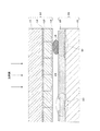
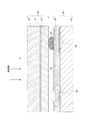
すなわち、この発明の光または放射線検出器の製造方法は、光または放射線の入射により電荷を生成する多結晶の半導体膜と、その半導体膜を積層形成するために支持する支持基板とを備え、前記半導体膜の結晶粒が厚み方向に結晶粒界が存在しないように連続的に形成された光または放射線検出器を製造する製造方法であって、前記半導体膜を形成する際に、ダミー基板に所定厚みの半導体膜を蒸着によって形成した後に、そのダミー基板から前記支持基板に交換して、その支持基板に半導体膜を蒸着によって引き続き形成し、かつ、蒸着源と、前記支持基板またはダミー基板とを近接させて、その基板の表面に前記蒸着源の昇華物を堆積させる近接昇華法によって、前記支持基板に形成されるべき前記半導体膜または前記ダミー基板に形成されるべき前記半導体膜を形成することを特徴とするものである。
この発明では、このような蒸着する手法の中でも、蒸着源と、支持基板またはダミー基板とを近接させて、その基板の表面に蒸着源の昇華物を堆積させる近接昇華法を採用している。すなわち、近接昇華法の場合には、支持基板またはダミー基板に半導体膜が形成される。この近接昇華法では蒸着源が近接にあるので、比較的に容易に大面積の半導体膜を形成することができる。
さらに、蒸着源と、支持基板またはダミー基板とを近接させて、その基板の表面に蒸着源の昇華物を堆積させる近接昇華法を採用しており、近接昇華法の場合には、支持基板またはダミー基板に半導体膜が形成される。この近接昇華法では蒸着源が近接にあるので、比較的に容易に大面積の半導体膜を形成することができる。
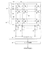
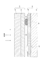
図1は、実施例に係る直接変換型のフラットパネル型X線検出器(以下、適宜「FPD」と略記する)の概略断面図であり、図2は、フラットパネル型X線検出器(FPD)のアクティブマトリックス基板の等価回路を示すブロック図である。本実施例では、放射線検出器としてフラットパネル型X線検出器(FPD)を例に採って説明する。
13 … (放射線感応型の)半導体
20 … アクティブマトリックス基板
22 … 電荷蓄積容量素子
23 … TFT(薄膜電界効果トランジスタ)素子
26 … ゲート線
27 … データ線
Claims (1)
- 光または放射線の入射により電荷を生成する多結晶の半導体膜と、その半導体膜を積層形成するために支持する支持基板とを備え、前記半導体膜の結晶粒が厚み方向に結晶粒界が存在しないように連続的に形成された光または放射線検出器を製造する製造方法であって、前記半導体膜を形成する際に、ダミー基板に所定厚みの半導体膜を蒸着によって形成した後に、そのダミー基板から前記支持基板に交換して、その支持基板に半導体膜を蒸着によって引き続き形成し、かつ、蒸着源と、前記支持基板またはダミー基板とを近接させて、その基板の表面に前記蒸着源の昇華物を堆積させる近接昇華法によって、前記支持基板に形成されるべき前記半導体膜または前記ダミー基板に形成されるべき前記半導体膜を形成することを特徴とする光または放射線検出器の製造方法。
Priority Applications (4)
| Application Number | Priority Date | Filing Date | Title |
|---|---|---|---|
| JP2006249736A JP4106397B2 (ja) | 2006-09-14 | 2006-09-14 | 光または放射線検出器の製造方法 |
| PCT/JP2007/058064 WO2008032461A1 (en) | 2006-09-14 | 2007-04-12 | Method for fabricating light or radiation detector, and light or radiation detector |
| CN2007800342878A CN101517751B (zh) | 2006-09-14 | 2007-04-12 | 光或放射线检测器的制造方法及光或放射线检测器 |
| US12/441,312 US7736941B2 (en) | 2006-09-14 | 2007-04-12 | Light or radiation detector manufacturing method |
Applications Claiming Priority (1)
| Application Number | Priority Date | Filing Date | Title |
|---|---|---|---|
| JP2006249736A JP4106397B2 (ja) | 2006-09-14 | 2006-09-14 | 光または放射線検出器の製造方法 |
Publications (2)
| Publication Number | Publication Date |
|---|---|
| JP2008071961A JP2008071961A (ja) | 2008-03-27 |
| JP4106397B2 true JP4106397B2 (ja) | 2008-06-25 |
Family
ID=39183530
Family Applications (1)
| Application Number | Title | Priority Date | Filing Date |
|---|---|---|---|
| JP2006249736A Expired - Fee Related JP4106397B2 (ja) | 2006-09-14 | 2006-09-14 | 光または放射線検出器の製造方法 |
Country Status (4)
| Country | Link |
|---|---|
| US (1) | US7736941B2 (ja) |
| JP (1) | JP4106397B2 (ja) |
| CN (1) | CN101517751B (ja) |
| WO (1) | WO2008032461A1 (ja) |
Families Citing this family (24)
| Publication number | Priority date | Publication date | Assignee | Title |
|---|---|---|---|---|
| JP2012508375A (ja) * | 2008-11-10 | 2012-04-05 | コーニンクレッカ フィリップス エレクトロニクス エヌ ヴィ | 放射線検出器用のコンバータ・エレメント |
| JP4835710B2 (ja) * | 2009-03-17 | 2011-12-14 | ソニー株式会社 | 固体撮像装置、固体撮像装置の製造方法、固体撮像装置の駆動方法、及び電子機器 |
| JP5610798B2 (ja) * | 2010-03-12 | 2014-10-22 | キヤノン株式会社 | シンチレータの製造方法 |
| JP5423880B2 (ja) * | 2010-04-07 | 2014-02-19 | 株式会社島津製作所 | 放射線検出器およびそれを製造する方法 |
| CN102332479A (zh) * | 2010-07-13 | 2012-01-25 | 李硕 | 叠层薄膜太阳能电池 |
| GB201021112D0 (en) | 2010-12-13 | 2011-01-26 | Ntnu Technology Transfer As | Nanowires |
| US20140246744A1 (en) * | 2011-04-01 | 2014-09-04 | Shimadzu Corporation | Method of manufacturing radiation detector and radiation detector |
| WO2013088625A1 (ja) * | 2011-12-16 | 2013-06-20 | 株式会社島津製作所 | 放射線検出器の製造方法 |
| JP5664798B2 (ja) * | 2011-12-16 | 2015-02-04 | 株式会社島津製作所 | 放射線検出器とその製造方法 |
| JP5895650B2 (ja) * | 2012-03-28 | 2016-03-30 | ソニー株式会社 | 撮像装置および撮像表示システム |
| GB201211038D0 (en) | 2012-06-21 | 2012-08-01 | Norwegian Univ Sci & Tech Ntnu | Solar cells |
| CN104164649A (zh) * | 2013-05-16 | 2014-11-26 | 朱兴华 | 大面积碘化铅厚膜的制备方法及其实施设备 |
| GB201311101D0 (en) | 2013-06-21 | 2013-08-07 | Norwegian Univ Sci & Tech Ntnu | Semiconducting Films |
| JP6163936B2 (ja) * | 2013-07-22 | 2017-07-19 | 株式会社島津製作所 | 二次元放射線検出器の製造方法 |
| DE102014114575A1 (de) | 2014-06-23 | 2015-12-24 | Von Ardenne Gmbh | Transportvorrichtung, Prozessieranordnung und Beschichtungsverfahren |
| KR20180055803A (ko) | 2015-07-13 | 2018-05-25 | 크래요나노 에이에스 | 나노와이어/나노피라미드 형상 발광 다이오드 및 광검출기 |
| KR102564288B1 (ko) | 2015-07-13 | 2023-08-04 | 크래요나노 에이에스 | 그라파이트 기판상에서 성장한 나노와이어 또는 나노피라미드 |
| EA201890238A1 (ru) | 2015-07-31 | 2018-08-31 | Крайонано Ас | Способ выращивания нанопроволок или нанопирамидок на графитовых подложках |
| CA3037960A1 (en) | 2016-11-30 | 2018-06-07 | The Research Foundation For The State University Of New York | Hybrid active matrix flat panel detector system and method |
| US10651334B2 (en) * | 2017-02-14 | 2020-05-12 | International Business Machines Corporation | Semitransparent chalcogen solar cell |
| GB201703196D0 (en) * | 2017-02-28 | 2017-04-12 | Univ Of Sussex | X-ray and gammay-ray photodiode |
| GB201705755D0 (en) | 2017-04-10 | 2017-05-24 | Norwegian Univ Of Science And Tech (Ntnu) | Nanostructure |
| CN110230039B (zh) * | 2019-07-02 | 2020-07-10 | 中南大学 | 一种单层硫化钼调控碘化铅生长的方法 |
| GB201913701D0 (en) | 2019-09-23 | 2019-11-06 | Crayonano As | Composition of matter |
Family Cites Families (12)
| Publication number | Priority date | Publication date | Assignee | Title |
|---|---|---|---|---|
| JPH0878707A (ja) | 1994-09-08 | 1996-03-22 | Japan Energy Corp | 太陽電池の製造方法 |
| JPH10303441A (ja) | 1997-04-28 | 1998-11-13 | Matsushita Denchi Kogyo Kk | 太陽電池及びその製造方法 |
| WO1997045880A1 (fr) | 1996-05-28 | 1997-12-04 | Matsushita Battery Industrial Co., Ltd. | Procede de formation d'un film au tellure de cadmium et d'une photopile mettant en oeuvre ce film |
| JPH1174551A (ja) | 1997-08-28 | 1999-03-16 | Matsushita Denchi Kogyo Kk | 硫化物半導体膜の製造方法および太陽電池 |
| JPH11152564A (ja) * | 1997-11-17 | 1999-06-08 | Murata Mfg Co Ltd | プリスパッタ方法および装置 |
| JP3792433B2 (ja) | 1999-04-19 | 2006-07-05 | シャープ株式会社 | 光又は放射線検出素子ならびに二次元画像検出器の製造方法 |
| JP2000357810A (ja) | 1999-06-16 | 2000-12-26 | Matsushita Battery Industrial Co Ltd | テルル化カドミウム膜の製造方法および太陽電池 |
| JP4092825B2 (ja) | 1999-09-30 | 2008-05-28 | 株式会社島津製作所 | アレイ型検出装置、およびその製造方法 |
| JP2004138472A (ja) | 2002-10-17 | 2004-05-13 | Mitsubishi Heavy Ind Ltd | 放射線検出素子、放射線検出装置、放射線ct装置及び放射線検査装置 |
| US7223989B2 (en) | 2003-10-21 | 2007-05-29 | Konica Minolta Medical & Graphic, Inc. | Radiation image conversion panel |
| JP3997978B2 (ja) | 2003-10-21 | 2007-10-24 | コニカミノルタエムジー株式会社 | 放射線画像変換パネル |
| JP2005298894A (ja) | 2004-04-12 | 2005-10-27 | Fujitsu Ltd | ターゲットのクリーニング方法及び物理的堆積装置 |
-
2006
- 2006-09-14 JP JP2006249736A patent/JP4106397B2/ja not_active Expired - Fee Related
-
2007
- 2007-04-12 WO PCT/JP2007/058064 patent/WO2008032461A1/ja not_active Ceased
- 2007-04-12 US US12/441,312 patent/US7736941B2/en not_active Expired - Fee Related
- 2007-04-12 CN CN2007800342878A patent/CN101517751B/zh not_active Expired - Fee Related
Also Published As
| Publication number | Publication date |
|---|---|
| CN101517751A (zh) | 2009-08-26 |
| WO2008032461A1 (en) | 2008-03-20 |
| US20100029037A1 (en) | 2010-02-04 |
| JP2008071961A (ja) | 2008-03-27 |
| US7736941B2 (en) | 2010-06-15 |
| CN101517751B (zh) | 2011-12-07 |
Similar Documents
| Publication | Publication Date | Title |
|---|---|---|
| JP4106397B2 (ja) | 光または放射線検出器の製造方法 | |
| JP4269653B2 (ja) | 放射線検出器の製造方法 | |
| CA2669678C (en) | Photodetector/imaging device with avalanche gain | |
| US8405037B2 (en) | Radiation detector manufacturing method, a radiation detector, and a radiographic apparatus | |
| JP2001242255A (ja) | 放射線検出器および放射線撮像装置 | |
| JPH04214669A (ja) | 固体放射線検出装置 | |
| US20210242415A1 (en) | Fabrication method for fused multi-layer amorphous selenium sensor | |
| KR100598577B1 (ko) | 방사선 검출기 | |
| US7420178B2 (en) | Radiation detector and radiation imaging device equipped with the same | |
| CN103081127B (zh) | 放射线检测器的制造方法 | |
| JP4092825B2 (ja) | アレイ型検出装置、およびその製造方法 | |
| WO2012004913A1 (ja) | 放射線検出器およびそれを製造する方法 | |
| Scheuermann et al. | Low dose digital X-ray imaging with avalanche amorphous selenium | |
| JP2005019543A (ja) | 二次元半導体検出器および二次元撮像装置 | |
| JP2007235039A (ja) | 放射線検出器の製造方法 | |
| JP5621919B2 (ja) | 放射線検出器の製造方法および放射線検出器 | |
| JP2012194046A (ja) | 放射線検出器の製造方法 | |
| HK40019087B (en) | Fabrication method for fused multi-layer amorphous selenium sensor | |
| HK40019087A (en) | Fabrication method for fused multi-layer amorphous selenium sensor | |
| JP2005033003A (ja) | 放射線検出器およびその製造方法 | |
| JP2012063166A (ja) | 放射線検出器の製造方法および放射線検出器 |
Legal Events
| Date | Code | Title | Description |
|---|---|---|---|
| A521 | Request for written amendment filed |
Free format text: JAPANESE INTERMEDIATE CODE: A523 Effective date: 20080107 |
|
| TRDD | Decision of grant or rejection written | ||
| A01 | Written decision to grant a patent or to grant a registration (utility model) |
Free format text: JAPANESE INTERMEDIATE CODE: A01 Effective date: 20080205 |
|
| A61 | First payment of annual fees (during grant procedure) |
Free format text: JAPANESE INTERMEDIATE CODE: A61 Effective date: 20080214 |
|
| FPAY | Renewal fee payment (event date is renewal date of database) |
Free format text: PAYMENT UNTIL: 20110411 Year of fee payment: 3 |
|
| R150 | Certificate of patent or registration of utility model |
Ref document number: 4106397 Country of ref document: JP Free format text: JAPANESE INTERMEDIATE CODE: R150 Free format text: JAPANESE INTERMEDIATE CODE: R150 |
|
| FPAY | Renewal fee payment (event date is renewal date of database) |
Free format text: PAYMENT UNTIL: 20110411 Year of fee payment: 3 |
|
| FPAY | Renewal fee payment (event date is renewal date of database) |
Free format text: PAYMENT UNTIL: 20120411 Year of fee payment: 4 |
|
| R250 | Receipt of annual fees |
Free format text: JAPANESE INTERMEDIATE CODE: R250 |
|
| FPAY | Renewal fee payment (event date is renewal date of database) |
Free format text: PAYMENT UNTIL: 20120411 Year of fee payment: 4 |
|
| FPAY | Renewal fee payment (event date is renewal date of database) |
Free format text: PAYMENT UNTIL: 20130411 Year of fee payment: 5 |
|
| R250 | Receipt of annual fees |
Free format text: JAPANESE INTERMEDIATE CODE: R250 |
|
| FPAY | Renewal fee payment (event date is renewal date of database) |
Free format text: PAYMENT UNTIL: 20130411 Year of fee payment: 5 |
|
| FPAY | Renewal fee payment (event date is renewal date of database) |
Free format text: PAYMENT UNTIL: 20140411 Year of fee payment: 6 |
|
| R250 | Receipt of annual fees |
Free format text: JAPANESE INTERMEDIATE CODE: R250 |
|
| R250 | Receipt of annual fees |
Free format text: JAPANESE INTERMEDIATE CODE: R250 |
|
| R250 | Receipt of annual fees |
Free format text: JAPANESE INTERMEDIATE CODE: R250 |
|
| R250 | Receipt of annual fees |
Free format text: JAPANESE INTERMEDIATE CODE: R250 |
|
| R250 | Receipt of annual fees |
Free format text: JAPANESE INTERMEDIATE CODE: R250 |
|
| R250 | Receipt of annual fees |
Free format text: JAPANESE INTERMEDIATE CODE: R250 |
|
| LAPS | Cancellation because of no payment of annual fees |