JP4106397B2 - Method for manufacturing light or radiation detector - Google Patents
Method for manufacturing light or radiation detector Download PDFInfo
- Publication number
- JP4106397B2 JP4106397B2 JP2006249736A JP2006249736A JP4106397B2 JP 4106397 B2 JP4106397 B2 JP 4106397B2 JP 2006249736 A JP2006249736 A JP 2006249736A JP 2006249736 A JP2006249736 A JP 2006249736A JP 4106397 B2 JP4106397 B2 JP 4106397B2
- Authority
- JP
- Japan
- Prior art keywords
- substrate
- semiconductor
- radiation
- semiconductor film
- vapor deposition
- Prior art date
- Legal status (The legal status is an assumption and is not a legal conclusion. Google has not performed a legal analysis and makes no representation as to the accuracy of the status listed.)
- Expired - Fee Related
Links
Images


Classifications
-
- H—ELECTRICITY
- H10—SEMICONDUCTOR DEVICES; ELECTRIC SOLID-STATE DEVICES NOT OTHERWISE PROVIDED FOR
- H10F—INORGANIC SEMICONDUCTOR DEVICES SENSITIVE TO INFRARED RADIATION, LIGHT, ELECTROMAGNETIC RADIATION OF SHORTER WAVELENGTH OR CORPUSCULAR RADIATION
- H10F39/00—Integrated devices, or assemblies of multiple devices, comprising at least one element covered by group H10F30/00, e.g. radiation detectors comprising photodiode arrays
- H10F39/011—Manufacture or treatment of image sensors covered by group H10F39/12
-
- G—PHYSICS
- G01—MEASURING; TESTING
- G01T—MEASUREMENT OF NUCLEAR OR X-RADIATION
- G01T1/00—Measuring X-radiation, gamma radiation, corpuscular radiation, or cosmic radiation
- G01T1/16—Measuring radiation intensity
- G01T1/24—Measuring radiation intensity with semiconductor detectors
-
- H—ELECTRICITY
- H10—SEMICONDUCTOR DEVICES; ELECTRIC SOLID-STATE DEVICES NOT OTHERWISE PROVIDED FOR
- H10F—INORGANIC SEMICONDUCTOR DEVICES SENSITIVE TO INFRARED RADIATION, LIGHT, ELECTROMAGNETIC RADIATION OF SHORTER WAVELENGTH OR CORPUSCULAR RADIATION
- H10F71/00—Manufacture or treatment of devices covered by this subclass
- H10F71/139—Manufacture or treatment of devices covered by this subclass using temporary substrates
-
- H—ELECTRICITY
- H10—SEMICONDUCTOR DEVICES; ELECTRIC SOLID-STATE DEVICES NOT OTHERWISE PROVIDED FOR
- H10F—INORGANIC SEMICONDUCTOR DEVICES SENSITIVE TO INFRARED RADIATION, LIGHT, ELECTROMAGNETIC RADIATION OF SHORTER WAVELENGTH OR CORPUSCULAR RADIATION
- H10F39/00—Integrated devices, or assemblies of multiple devices, comprising at least one element covered by group H10F30/00, e.g. radiation detectors comprising photodiode arrays
- H10F39/80—Constructional details of image sensors
- H10F39/809—Constructional details of image sensors of hybrid image sensors
-
- Y—GENERAL TAGGING OF NEW TECHNOLOGICAL DEVELOPMENTS; GENERAL TAGGING OF CROSS-SECTIONAL TECHNOLOGIES SPANNING OVER SEVERAL SECTIONS OF THE IPC; TECHNICAL SUBJECTS COVERED BY FORMER USPC CROSS-REFERENCE ART COLLECTIONS [XRACs] AND DIGESTS
- Y02—TECHNOLOGIES OR APPLICATIONS FOR MITIGATION OR ADAPTATION AGAINST CLIMATE CHANGE
- Y02E—REDUCTION OF GREENHOUSE GAS [GHG] EMISSIONS, RELATED TO ENERGY GENERATION, TRANSMISSION OR DISTRIBUTION
- Y02E10/00—Energy generation through renewable energy sources
- Y02E10/50—Photovoltaic [PV] energy
Landscapes
- Physics & Mathematics (AREA)
- Health & Medical Sciences (AREA)
- Life Sciences & Earth Sciences (AREA)
- General Physics & Mathematics (AREA)
- High Energy & Nuclear Physics (AREA)
- Molecular Biology (AREA)
- Spectroscopy & Molecular Physics (AREA)
- Solid State Image Pick-Up Elements (AREA)
- Measurement Of Radiation (AREA)
- Light Receiving Elements (AREA)
- Physical Vapour Deposition (AREA)
Description
この発明は、医療分野,工業分野,さらには、原子力分野などに用いられる光または放射線検出器の製造方法に関する。 The present invention relates to a method for manufacturing a light or radiation detector used in the medical field, the industrial field, and the nuclear field.
光または放射線検出器は、光または放射線の入射により電荷を生成する半導体と、その半導体を積層形成するために支持する支持基板とを備えている。放射線(例えばX線)検出器には、放射線(例えばX線)の入射により光を一旦生成して、その光から電荷を生成することで、放射線から電荷に間接的に変換して放射線を検出する「間接変換型」の検出器と、放射線の入射により電荷を生成することで、放射線から電荷に直接的に変換して放射線を検出する「直接変換型」の検出器とがある。「直接変換型」の検出器では、電荷を生成する半導体は放射線感応型の半導体である。 The light or radiation detector includes a semiconductor that generates electric charges upon incidence of light or radiation, and a support substrate that supports the semiconductor to form a stacked layer. Radiation (for example, X-ray) detectors detect light by indirectly converting radiation into charge by generating light once by the incidence of radiation (for example, X-ray) and generating charge from that light. There are “indirect conversion type” detectors, and “direct conversion type” detectors that detect radiation by directly converting radiation into electric charge by generating charges by the incidence of radiation. In a “direct conversion type” detector, the semiconductor that generates the charge is a radiation sensitive semiconductor.
この放射線感応型の半導体として、物理蒸着法(Physical Vapor Deposition :PVD)によって形成されたCdTe,ZnTe,HgI2,PbI2,PbO,BiI3,TlBr,Se,Si,GaAs,InP等の膜が使用もしくは検討されている。例えば、CdTeのような高感度材料の成膜方法としてスパッタリング・CVD・昇華法・化学堆積法等が知られているが、これらの方法ではいずれも多結晶膜が得られる。多結晶膜の光または放射線に対する検出特性は、膜の結晶形態に大きく依存し、したがって膜の形成条件に大きく依存する。 As this radiation-sensitive semiconductor, a film of CdTe, ZnTe, HgI 2 , PbI 2 , PbO, BiI 3 , TlBr, Se, Si, GaAs, InP or the like formed by physical vapor deposition (PVD) is used. Used or considered. For example, sputtering, CVD, sublimation, chemical deposition, and the like are known as film formation methods for high-sensitivity materials such as CdTe. In any of these methods, a polycrystalline film can be obtained. The detection characteristics of the polycrystalline film with respect to light or radiation largely depend on the crystalline form of the film, and therefore greatly depend on the film forming conditions.
ところで、物理蒸着法の中で「近接昇華法」と呼ばれる方法がある。この近接昇華法は、蒸着源であるソースと半導体を表面に形成させる対象物である支持基板とを近接させて、その支持基板の表面にソースの昇華物による半導体を形成する方法である。この近接昇華法ではソースが近接にあるので、比較的に容易に大面積の半導体を形成することができる。 By the way, there is a method called “proximity sublimation method” in physical vapor deposition. This proximity sublimation method is a method in which a source that is a vapor deposition source and a support substrate that is an object on which a semiconductor is formed are brought close to each other, and a semiconductor by a sublimate of the source is formed on the surface of the support substrate. In this proximity sublimation method, since the source is close, a semiconductor with a large area can be formed relatively easily.
しかし、これらの方法に代表される物理蒸着法によって形成される半導体膜では、ソースの表面層から初期に基板界面近傍に形成される膜は結晶性が悪い。特に、近接昇華法で形成されたCdZnTe膜では、ソースの表面層から初期に基板に形成される膜は結晶性が悪く、検出特性を劣化させる原因となることを実験的に確認している。 However, in a semiconductor film formed by a physical vapor deposition method typified by these methods, a film formed in the vicinity of the substrate interface in the initial stage from the surface layer of the source has poor crystallinity. In particular, in the CdZnTe film formed by the proximity sublimation method, it has been experimentally confirmed that the film formed on the substrate initially from the surface layer of the source has poor crystallinity and causes deterioration in detection characteristics.
そこで、蒸着源であるソースと基板の成膜面との間に遮蔽する手段を設けることで、初期に蒸着形成される膜をカットした後に、基板の表面に半導体膜を形成する手法がある(例えば、非特許文献1参照)。この手法によれば、初期状態ではソースに不純物が混ざっているので、その初期において遮蔽することで、初期に蒸着形成されるべき不良膜をカットする。したがって、それ以降に遮蔽を解除することで、解除後に形成される半導体膜は高品質なものとなり、検出特性を向上させることができる。
このような遮蔽する手法によって、高品質な半導体を備えた光または放射線検出器を実現することができるが、上述した手法以外の手法においても、高品質な半導体を備えた光または放射線検出器を実現することが望まれる。 By such a shielding method, a light or radiation detector provided with a high-quality semiconductor can be realized, but in a method other than the method described above, a light or radiation detector provided with a high-quality semiconductor is also used. Realization is desired.
この発明は、このような事情に鑑みてなされたものであって、高品質な半導体を備えた検出器を実現することができる光または放射線検出器の製造方法を提供することを目的とする。 This invention is made | formed in view of such a situation, Comprising: It aims at providing the manufacturing method of the light or radiation detector which can implement | achieve the detector provided with the high quality semiconductor.
この発明は、このような目的を達成するために、次のような構成をとる。
すなわち、この発明の光または放射線検出器の製造方法は、光または放射線の入射により電荷を生成する多結晶の半導体膜と、その半導体膜を積層形成するために支持する支持基板とを備え、前記半導体膜の結晶粒が厚み方向に結晶粒界が存在しないように連続的に形成された光または放射線検出器を製造する製造方法であって、前記半導体膜を形成する際に、ダミー基板に所定厚みの半導体膜を蒸着によって形成した後に、そのダミー基板から前記支持基板に交換して、その支持基板に半導体膜を蒸着によって引き続き形成し、かつ、蒸着源と、前記支持基板またはダミー基板とを近接させて、その基板の表面に前記蒸着源の昇華物を堆積させる近接昇華法によって、前記支持基板に形成されるべき前記半導体膜または前記ダミー基板に形成されるべき前記半導体膜を形成することを特徴とするものである。
In order to achieve such an object, the present invention has the following configuration.
That is, the method for manufacturing a light or radiation detector according to the present invention includes a polycrystalline semiconductor film that generates an electric charge upon incidence of light or radiation, and a support substrate that supports the semiconductor film to form a stacked layer. A manufacturing method for manufacturing a light or radiation detector in which crystal grains of a semiconductor film are continuously formed so that there are no crystal grain boundaries in the thickness direction. After forming a semiconductor film having a thickness by vapor deposition, the dummy substrate is replaced with the support substrate, a semiconductor film is continuously formed on the support substrate by vapor deposition, and a vapor deposition source and the support substrate or dummy substrate are formed. Formed on the semiconductor film or the dummy substrate to be formed on the support substrate by a proximity sublimation method in which a sublimate of the evaporation source is deposited on the surface of the substrate. It is characterized in forming said semiconductor film to be.
この発明の光または放射線検出器によれば、多結晶の半導体膜を形成する際に、ダミー基板に所定厚みの半導体膜を蒸着によって形成した後に、そのダミー基板から支持基板に交換して、その支持基板に半導体膜を蒸着によって引き続き形成する。ダミー基板に所定厚みの半導体膜を蒸着によって形成する際は初期状態なので、本来であれば形成される不良膜がダミー基板に形成される。その後に、交換された支持基板には初期状態でない半導体膜が形成されるので、従来よりも高品質な半導体を備えた検出器を実現することができる。また、このようにして製造された半導体膜は、半導体膜の結晶粒が厚み方向に結晶粒界が存在しないように連続的に形成されたものとなる。
この発明では、このような蒸着する手法の中でも、蒸着源と、支持基板またはダミー基板とを近接させて、その基板の表面に蒸着源の昇華物を堆積させる近接昇華法を採用している。すなわち、近接昇華法の場合には、支持基板またはダミー基板に半導体膜が形成される。この近接昇華法では蒸着源が近接にあるので、比較的に容易に大面積の半導体膜を形成することができる。
According to the light or radiation detector of the present invention, when a polycrystalline semiconductor film is formed, a semiconductor film having a predetermined thickness is formed on the dummy substrate by vapor deposition, and then the dummy substrate is replaced with a support substrate. A semiconductor film is subsequently formed on the support substrate by vapor deposition. Since a semiconductor film having a predetermined thickness is formed by vapor deposition on the dummy substrate, it is in an initial state, so that a defective film that is originally formed is formed on the dummy substrate. After that, since the semiconductor film which is not in the initial state is formed on the replaced support substrate, it is possible to realize a detector including a semiconductor having a higher quality than the conventional one. In addition, the semiconductor film manufactured in this way is formed continuously so that crystal grains of the semiconductor film do not have crystal grain boundaries in the thickness direction.
In the present invention, among such techniques for vapor deposition, a proximity sublimation method is adopted in which a vapor deposition source and a support substrate or a dummy substrate are brought close to each other, and a sublimate of the vapor deposition source is deposited on the surface of the substrate. That is, in the case of the proximity sublimation method, a semiconductor film is formed on a support substrate or a dummy substrate. In this proximity sublimation method, since the deposition source is in the vicinity, a semiconductor film having a large area can be formed relatively easily.
この発明に係る光または放射線検出器の製造方法によれば、多結晶の半導体膜を形成する際に、ダミー基板に所定厚みの半導体膜を蒸着によって形成した後に、そのダミー基板から支持基板に交換して、その支持基板に半導体膜を蒸着によって引き続き形成することで、従来よりも高品質な半導体を備えた検出器を実現することができる。また、このようにして製造された半導体膜は、半導体膜の結晶粒が厚み方向に結晶粒界が存在しないように連続的に形成されたものとなる。
さらに、蒸着源と、支持基板またはダミー基板とを近接させて、その基板の表面に蒸着源の昇華物を堆積させる近接昇華法を採用しており、近接昇華法の場合には、支持基板またはダミー基板に半導体膜が形成される。この近接昇華法では蒸着源が近接にあるので、比較的に容易に大面積の半導体膜を形成することができる。
According to the method for manufacturing a light or radiation detector according to the present invention, when a polycrystalline semiconductor film is formed, a semiconductor film having a predetermined thickness is formed on the dummy substrate by vapor deposition, and then the dummy substrate is replaced with a support substrate. Then, by continuously forming a semiconductor film on the supporting substrate by vapor deposition, it is possible to realize a detector having a higher quality semiconductor than the conventional one. In addition, the semiconductor film manufactured in this way is formed continuously so that crystal grains of the semiconductor film do not have crystal grain boundaries in the thickness direction.
Further, a proximity sublimation method is adopted in which a vapor deposition source and a support substrate or a dummy substrate are brought close to each other, and a sublimate of the vapor deposition source is deposited on the surface of the substrate. A semiconductor film is formed on the dummy substrate. In this proximity sublimation method, since the deposition source is in the vicinity, a semiconductor film having a large area can be formed relatively easily.
以下、図面を参照してこの発明の実施例を説明する。
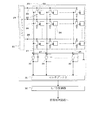
図1は、実施例に係る直接変換型のフラットパネル型X線検出器(以下、適宜「FPD」と略記する)の概略断面図であり、図2は、フラットパネル型X線検出器(FPD)のアクティブマトリックス基板の等価回路を示すブロック図である。本実施例では、放射線検出器としてフラットパネル型X線検出器(FPD)を例に採って説明する。
Embodiments of the present invention will be described below with reference to the drawings.
FIG. 1 is a schematic cross-sectional view of a direct conversion flat panel X-ray detector (hereinafter abbreviated as “FPD” where appropriate) according to an embodiment, and FIG. 2 is a flat panel X-ray detector (FPD). 2 is a block diagram showing an equivalent circuit of the active matrix substrate of FIG. In the present embodiment, a flat panel X-ray detector (FPD) will be described as an example of the radiation detector.
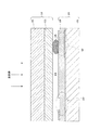
本実施例に係るFPDは、図1に示すように、検出器基板10とアクティブマトリックス基板20とを備えている。検出器基板10は、導電性グラファイト基板11と放射線感応型の半導体13と2つのキャリア選択性の阻止層12,14とを備えている。アクティブマトリックス基板20は、ガラス基板21に電荷蓄積容量素子22やTFT(薄膜電界効果トランジスタ)素子23や画素電極24などがパターン形成されて構成されている。検出器基板10とアクティブマトリックス基板20との間にはバンプ電極15を介在させており、バンプ電極15を介して各画素電極24毎に画素電極24がキャリア選択性の阻止層14に接続されている。導電性グラファイト基板11は、この発明における支持基板に相当し、放射線感応型の半導体13は、この発明における半導体膜に相当し、アクティブマトリックス基板20は、この発明におけるアクティブマトリックス基板に相当し、電荷蓄積容量素子22は、この発明における電荷蓄積容量素子に相当し、TFT素子23は、この発明におけるスイッチング素子に相当する。
The FPD according to this embodiment includes a
図1に示すように、検出器基板10とアクティブマトリックス基板20とを、バンプ電極15を介して貼り合わせることで、アクティブマトリックス基板20は入射側に半導体13を積層形成する。
As shown in FIG. 1, the
半導体13は、放射線(実施例ではX線)の入射により電荷を生成する。導電性グラファイト基板11は、半導体13を積層形成するために支持し、バイアス電圧印加用の共通電極としての機能を有する。
The
電荷蓄積容量素子22は、半導体13によって生成された電荷を蓄積する。TFT素子23は、蓄積された電荷をスイッチングによって読み出す。ガラス基板21の表面には、電荷蓄積容量素子22やTFT素子23や画素電極24などがパターン形成され、電荷蓄積容量素子22の各電極や、ゲート電極/ソース・ドレイン電極間に絶縁層25が介在するように積層形成されている。電荷蓄積容量素子22の入射側の電極は、画素電極24であって、その一部がTFT素子23のソース電極を形成している。すなわち、電荷蓄積容量素子22の画素電極24はTFT素子23のソース電極に接続されている。また、TFT素子23のゲート電極は、ゲート線26(図2を参照)に接続され、TFT素子23のドレイン電極はデータ線27(図2を参照)に接続される。
The charge
図2に示すように、これらのゲート線26およびデータ線27のような電極配線、TFT素子23および電荷蓄積容量素子22を2次元状マトリックス配列で設定する。すなわち、ゲート線26は行毎に配設されているとともに、データ線27は列毎に配設されており、各ゲート線26と各データ線27とは互いに直交する。これらの2次元状マトリックス配列に応じて画素を割り当てることで、放射線で検出された電荷情報を画素値として変換することができる。すなわち、電荷蓄積容量素子22の画素電極24ごとに画素を割り当てる。したがって、画素領域28は全画素電極24が形成され得る領域となる。ゲート線26およびデータ線27は、この発明における電極配線に相当する。
As shown in FIG. 2, the electrode wiring such as the
ガラス基板21の表面には、上述した電荷蓄積容量素子22やTFT素子23などの他に、ゲートドライバ29や電荷電圧変換型増幅器30やマルチプレクサ31が画素領域28の周囲にパターン形成されている。なお、画素領域28の周辺には、A/D変換器32も配設されており、アクティブマトリックス基板20とは別基板で接続されている。なお、ゲートドライバ29、電荷電圧変換型増幅器30、マルチプレクサ31、A/D変換器32の一部または全部を、アクティブマトリックス基板20に内蔵してもよい。
On the surface of the
FPDによってX線を検出する際には、バイアス供給電源(図示省略)からバイアス電圧をバイアス電圧印加用の共通電極であるグラファイト基板11に印加する。バイアス電圧を印加した状態で、放射線(実施例ではX線)の入射に伴って放射線感応型の半導体13で電荷を生成する。この生成された電荷を、バンプ電極15を介して、収集電極でもある画素電極24で一旦収集する。収集された電荷を各画素電極24毎の放射線検出信号(実施例ではX線検出信号)として取り出す。
When X-rays are detected by the FPD, a bias voltage is applied from a bias supply power source (not shown) to the
具体的には、画素電極24で収集された電荷が電荷蓄積容量素子22で一旦蓄積される。そして、ゲートドライバ29からゲート線26を介して読み出し信号を各TFT素子23のゲート電極に順に与える。読み出し信号を与えることで、読み出し信号が与えられたTFT素子23がOFFからONに移行する。その移行したTFT素子23のドレイン電極に接続されたデータ線27がマルチプレクサ31によって順に切り換え接続されるのにしたがって、電荷蓄積容量素子22に蓄積された電荷を、TFT素子23からデータ線27を介して読み出す。読み出された電荷を電荷電圧変換型増幅器30で増幅して、マルチプレクサ31によって各画素電極24毎の放射線検出信号(実施例ではX線検出信号)としてA/D変換器32に送り出してアナログ値からディジタル値に変換する。
Specifically, the charges collected by the
例えば、FPDをX線透視撮影装置に備えた場合には、X線検出信号を後段の画像処理回路に送り込んで、画像処理を行って2次元X線透視画像等を出力する。2次元状マトリックス配列の各画素電極24は、放射線画像(ここでは2次元X線透視画像)の各画素にそれぞれ対応している。放射線検出信号(実施例ではX線検出信号)を取り出すことで、放射線の2次元強度分布に応じた放射線画像(ここでは2次元X線透視画像)を作成することができる。つまり、本実施例に係るFPDは、放射線(実施例ではX線)の2次元強度分布を検出することができる2次元アレイタイプの放射線検出器である。
For example, when an FPD is provided in an X-ray fluoroscopic apparatus, an X-ray detection signal is sent to an image processing circuit at a subsequent stage, image processing is performed, and a two-dimensional X-ray fluoroscopic image is output. Each
なお、電荷は一対の電子−正孔からなる。半導体13と電荷蓄積容量素子22とは、バンプ電極15を介して直列に接続された構造になっているので、例えばグラファイト基板11に負のバイアス電圧(−Vh)を印加すると、半導体13内で発生した電荷のうち、電子はバンプ電極15側に、正孔はグラファイト基板11側に移動する。その結果、電荷蓄積容量素子22に電荷が蓄積される。一方で、感度に寄与しない漏れ電荷が半導体13に注入され易くなっており、グラファイト基板11に負のバイアス電圧を印加する場合には、グラファイト基板11から半導体13へ電子が注入され易くなって、アクティブマトリックス基板20からバンプ電極15を介して半導体13へ正孔が注入され易くなっている。その結果、リーク電流が増加する。
The electric charge consists of a pair of electrons and holes. Since the
そこで、電荷の注入によるリーク電流を低減させるために、本実施例では、図1に示すように、グラファイト基板11と半導体13との間にキャリア選択性の阻止層12を形成するとともに、半導体13とアクティブマトリックス基板20との間にキャリア選択性の阻止層14を形成している。グラファイト基板11に負のバイアス電圧を印加する場合には、阻止層12は、グラファイト基板11からの電子の注入を阻止する電子阻止層として機能するとともに、阻止層14は、アクティブマトリックス基板20からの正孔の注入を阻止する正孔阻止層として機能する。
In order to reduce the leakage current due to the charge injection, in this embodiment, as shown in FIG. 1, a carrier-
このように、キャリア選択性の阻止層12,14を設けることによりリーク電流を低減させることができる。ここで言うキャリア選択性とは半導体中の電荷移動媒体(キャリア)である電子と正孔とで、電荷移動作用への寄与率が著しく異なる性質を指す。 Thus, the leakage current can be reduced by providing the carrier selective blocking layers 12 and 14. The carrier selectivity mentioned here refers to the property that the contribution rate to the charge transfer action is remarkably different between electrons and holes which are charge transfer media (carriers) in the semiconductor.
半導体13とキャリア選択性の阻止層12,14との組み合わせ方としては、次のような態様が挙げられる。グラファイト基板11に正のバイアス電圧を印加する場合には、阻止層12に電子の寄与率が大きい材料を使用する。これによりグラファイト基板11からの正孔の注入が阻止され、リーク電流を低減させることができる。阻止層14には正孔の寄与率が大きい材料を使用する。これによりアクティブマトリックス基板20からの電子の注入が阻止され、リーク電流を低減させることができる。
Examples of the combination of the
逆に、グラファイト基板11に負のバイアス電圧を印加する場合には、阻止層12に正孔の寄与率が大きい材料を使用する。上述したように、これによりグラファイト基板11からの電子の注入が阻止され、リーク電流を低減させることができる。阻止層14には電子の寄与率が大きい材料を使用する。上述したように、これによりアクティブマトリックス基板20からの正孔の注入が阻止され、リーク電流を低減させることができる。
Conversely, when a negative bias voltage is applied to the
阻止層12,14に用いられる半導体のうち、電子の寄与が大きいものとして、n型半導体であるCeO2 ,CdS,CdSe,ZnSe,ZnSのような多結晶半導体や、アルカリ金属やAsやTeをドープして正孔の寄与率を低下させたアモルファスSe等のアモルファス体が挙げられる。 Among the semiconductors used for the blocking layers 12 and 14, as semiconductors having a large contribution of electrons, polycrystalline semiconductors such as CeO 2 , CdS, CdSe, ZnSe, and ZnS that are n-type semiconductors, alkali metals, As, and Te are used. An amorphous body such as amorphous Se that has been doped to reduce the contribution ratio of holes can be used.
また、正孔の寄与が大きいものとして、p型半導体であるZnTeのような多結晶半導体や、ハロゲンをドープして電子の寄与率を低下させたアモルファスSe等のアモルファス体が挙げられる。 In addition, examples of a material having a large contribution of holes include a polycrystalline semiconductor such as ZnTe which is a p-type semiconductor, and an amorphous material such as amorphous Se doped with halogen to reduce the contribution of electrons.
さらに、Sb2 S3 ,CdTe,CdZnTe,PbI2 ,HgI2 ,TlBrや、ノンドープのアモルファスSeまたはSe化合物の場合、電子の寄与が大きいものと正孔の寄与が大きいもとの両方がある。これらの場合、成膜条件の調節で電子の寄与が大きいものでも、正孔の寄与が大きいものでも、選択形成することができる。 Furthermore, Sb 2 S 3, CdTe, CdZnTe, or PbI 2, HgI 2, TlBr, when the non-doped amorphous Se or Se compound, there is both a large contribution original electronic ones large contribution and the hole. In these cases, even if the contribution of electrons is large or the contribution of holes is large by adjusting the film forming conditions, selective formation can be performed.
本実施例のように、グラファイト基板11に負のバイアス電圧を印加する場合には、グラファイト基板11からの電子の注入を阻止する電子阻止層として阻止層12を機能させるために、正孔の寄与率が大きいZnTeで阻止層12を形成するとともに、アクティブマトリックス基板20からの正孔の注入を阻止する正孔阻止層として阻止層14を機能させるために、電子の寄与が大きいZnSで阻止層14を形成する。
When a negative bias voltage is applied to the
アクティブマトリックス基板20は、図1、図2に示すように、上述した電荷蓄積容量素子22やTFT素子23や画素電極24や絶縁層25やゲート線26やデータ線27やゲートドライバ29や電荷電圧変換型増幅器30やマルチプレクサ31をガラス基板21にスクリーン印刷等でパターン形成する。バンプ電極15をスクリーン印刷やスタッドバンプ工程により形成する。ガラス基板21の厚さは、例えば0.5mm〜1.5mm程度である。
As shown in FIGS. 1 and 2, the
半導体13の厚さは、通常、0.5mm〜1.5mm前後の厚膜(本実施例では約0.4mm)であり、面積は、例えば縦20cm〜50cm×横20cm〜50cm程度のものである。放射線感応型の半導体13は、高純度アモルファスセレン(a−Se),Na等のアルカリ金属やCl等のハロゲンもしくはAsやTeをドープしたセレンおよびセレン化合物のアモルファス半導体,CdTe,CdZnTe,PbI2 ,HgI2 ,TlBr等の非セレン系多結晶半導体のうちのいずれかであるのが好ましい。特に、CdTe,ZnTe,HgI2,PbI2,PbO,BiI3,TlBr,Se,Si,GaAs,InP、もしくはこれらを含む混合の結晶物(混晶)で半導体13を形成するのが好ましい。
The thickness of the
半導体13として、CdTe,ZnTe,HgI2,PbI2,PbO,BiI3,TlBr,GaAsを用いたものは、高感度でノイズ耐性の大きな検出器を得ることができる。Seを用いたものは、均一で大面積の検出器を容易に得ることができる。Si,InPを用いたものは、高エネルギー分解能の検出器を得ることができる。なお、半導体13としてCdZnTeを用いた場合には、CdZnTeは、CdTe,ZnTeの混合の結晶物(混晶)であるので、高感度でノイズ耐性の大きな検出器を得ることができる。
A semiconductor using CdTe, ZnTe, HgI 2 , PbI 2 , PbO, BiI 3 , TlBr, or GaAs as the
グラファイト基板11は、導電性を有するカーボンである。グラファイト基板11はバイアス電圧印加用の共通電極の機能を有するので、グラファイト以外で共通電極を形成してもよい。AlやMgAgなどの金属で共通電極を形成してもよいし、表面にITO(透明電極)などの電極を成膜したアルミナ基板などの電極基板で共通電極を形成してもよい。AlやMgAgなどの金属で共通電極を形成する場合には、共通電極の厚さは0.1μm程度の薄膜である。グラファイト基板11や電極基板で共通電極を形成する場合には、共通電極の厚さは2mm程度の厚膜である。また、阻止層12,14の厚さは、約200nm、抵抗率は1011Ω・cm台である。
The
次に、FPDの製造方法について説明する。アクティブマトリックス基板20側では、上述したように、電荷蓄積容量素子22やTFT素子23や画素電極24や絶縁層25やゲート線26やデータ線27やゲートドライバ29や電荷電圧変換型増幅器30やマルチプレクサ31をガラス基板21にスクリーン印刷等でパターン形成する。より具体的には、液晶表示用アクティブマトリックス基板と同様に、半導体薄膜製造技術や微細加工技術を用いてガラス基板21の表面に電荷蓄積容量素子22やTFT素子23を形成し、画素電極24との接続部分を除いて、その表面を絶縁層25で被膜する。画素領域28の周辺にあるゲートドライバ29や電荷電圧変換型増幅器30やマルチプレクサ31のような周辺回路を、シリコン等の半導体集積回路で構成し、異方導電性フィルム(ACF)などを介してゲート線26やゲート線27にそれぞれ接続する。
Next, an FPD manufacturing method will be described. On the
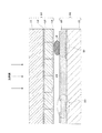
一方の検出器基板10側では、以下のように形成する。グラファイト基板11に阻止層12を積層形成する。阻止層14も含めて阻止層12を形成するには、物理蒸着(PVD)や化学析出法、電析法などを用いればよい。阻止層12が形成されたグラファイト基板11を、図3(b)に示すようにグラファイト基板Gとする。このグラファイト基板Gに半導体13を、図3(b)に示すような近接昇華法によって形成する。図3に示す近接昇華法については詳しく後述する。半導体13の形成後、表面を化学機械研磨(Chemical Mechanical Polishing :CMP)などの研磨等で平坦化処理する。そして、阻止層14を形成する。
On one
本実施例に係る近接昇華法について図3を参照して説明する。図3(a)に示すように、真空に脱気したチャンバCH内にCdZnTeの蒸着源であるソースSとダミー基板Dとを近接させて収容する。この場合の近接の距離は、形成される物質や成膜条件等で異なるが、2mm〜数mm程度の範囲である。また、ダミー基板Dは、交換される共通電極と同じ物質、同じサイズで形成されるのが好ましい。本実施例では共通電極はグラファイトであるので、グラファイトでダミー基板Dを形成する。 The proximity sublimation method according to the present embodiment will be described with reference to FIG. As shown in FIG. 3A, a source S as a CdZnTe vapor deposition source and a dummy substrate D are accommodated in a chamber CH that has been evacuated to a vacuum. The proximity distance in this case is in the range of about 2 mm to several mm, although it varies depending on the substance to be formed, film forming conditions, and the like. The dummy substrate D is preferably formed of the same material and the same size as the common electrode to be replaced. In this embodiment, since the common electrode is graphite, the dummy substrate D is formed of graphite.
ランプ加熱によってソースSを加熱するとソースSの固体が昇華して気化する。気化物はダミー基板Dに付着して再度固化してダミー基板Dの表面に形成される。ダミー基板Dに所定厚みのCdZnTeを形成した後に、図3(b)に示すように、そのダミー基板Dからグラファイト基板Gに交換して、そのグラファイト基板GにCdZnTeを引き続き形成する。 When the source S is heated by lamp heating, the solid of the source S is sublimated and vaporized. The vaporized material adheres to the dummy substrate D and solidifies again, and is formed on the surface of the dummy substrate D. After CdZnTe having a predetermined thickness is formed on the dummy substrate D, the dummy substrate D is replaced with the graphite substrate G, and CdZnTe is subsequently formed on the graphite substrate G, as shown in FIG.
ダミー基板Dからグラファイト基板Gに交換する際に、チャンバCH内の真空状態が保てなくなるが、CdZnTeの形成には支障がない。なお、グラファイト基板もダミー基板とともに予めチャンバCH内に収容するとともに、グラファイト基板をCdZnTeの形成に影響がない場所に退避させて収容し、交換時にグラファイト基板をソースに近接させるようにチャンバCH内で搬送してもよい。 When the dummy substrate D is replaced with the graphite substrate G, the vacuum state in the chamber CH cannot be maintained, but there is no problem in the formation of CdZnTe. The graphite substrate is also accommodated in the chamber CH together with the dummy substrate in advance, and the graphite substrate is retracted and accommodated in a place where there is no influence on the formation of CdZnTe. It may be conveyed.
上述した本実施例に係るFPDの製造方法によれば、半導体13を形成する際に、ダミー基板Dに所定厚みの半導体を蒸着によって形成した後に、そのダミー基板Dから支持基板であるグラファイト基板Gに交換して、そのグラファイト基板Gに半導体を蒸着によって引き続き形成する。ダミー基板Dに所定厚みの半導体を蒸着によって形成する際は初期状態なので、本来であれば形成される不良膜がダミー基板Dに形成される。その後に、交換されたグラファイト基板Dには初期状態でない半導体が形成されるので、従来よりも高品質な半導体13を備えた検出器を実現することができる。また、このようにして製造された半導体13は、少なくとも厚み方向に連続的に形成されたものとなる。かかる半導体13を検出器が備えることで、検出特性を向上させることができる。
According to the FPD manufacturing method according to the above-described embodiment, when the
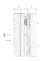
半導体13は、少なくとも厚み方向に連続的に形成されているケースとして、例えば、図1に示すように、厚み方向に直交する横方向にも半導体13は連続的に形成されているケースと、図4に示すように厚み方向に直交する横方向に半導体13は粒界によって断続的に形成されているケースとがある。これらはグラファイト基板11の温度によって、横方向の結晶粒径を制御することができ、温度が高いほど結晶粒径が大きくなる。したがって、図1に示すような厚み方向に直交する横方向にも連続的に形成された半導体13を実現するためには温度を高くして、図4に示すような厚み方向に直交する横方向に粒界によって断続的に形成された半導体13を実現するためには温度を低くする。
As the case where the
本実施例では、物理蒸着として近接昇華法を採用している。近接昇華法は、蒸着源であるソースと半導体13を表面に形成させる対象物であるグラファイト基板11とを近接させて、そのグラファイト基板11の表面にソースの昇華物による半導体13を形成する。この近接昇華法ではソースが近接にあるので、比較的に容易に大面積の半導体13を形成することができる。
In this embodiment, the proximity sublimation method is adopted as physical vapor deposition. In the proximity sublimation method, a source as a vapor deposition source and a
この発明は、上記実施形態に限られることはなく、下記のように変形実施することができる。 The present invention is not limited to the above-described embodiment, and can be modified as follows.
(1)上述した実施例では、直接変換型であったが、間接変換型にも適用できる。この場合には、半導体を、放射線の入射で生じた光の入射により電荷を生成する光電変換型(例えばフォトダイオード)で形成する。フォトダイオードの入射面にはシンチレータを積層形成してFPDを構成する。この場合にはシンチレータなどで放射線の入射により光を一旦生成して、その光から電荷をフォトダイオードが生成するので、FPDは、放射線から電荷に間接的に変換して放射線を検出する「間接変換型」となる。 (1) Although the direct conversion type is used in the above-described embodiments, the present invention can also be applied to an indirect conversion type. In this case, the semiconductor is formed of a photoelectric conversion type (for example, a photodiode) that generates charges by the incidence of light generated by the incidence of radiation. A scintillator is laminated on the incident surface of the photodiode to form an FPD. In this case, light is once generated by the incidence of radiation by a scintillator or the like, and the photodiode generates charge from the light. Therefore, the FPD detects radiation by indirectly converting radiation to charge. Type ".
(2)上述した実施例では、放射線検出器であったが、光検出器にも適用できる。この場合には、半導体を、光の入射により電荷を生成する光感応型で形成する。 (2) In the above-described embodiment, the radiation detector is used, but it can also be applied to a photodetector. In this case, the semiconductor is formed in a photosensitive type in which electric charges are generated by the incidence of light.
(3)上述した実施例では、フラットパネル型X線検出器に代表される放射線検出器は、2次元アレイタイプであったが、この発明の放射線検出器は、画素電極が1次元状マトリックス配列で形成されている1次元アレイタイプでもよいし、放射線検出信号取り出し用の電極が1個だけの非アレイタイプでもよい。 (3) In the above-described embodiment, the radiation detector represented by the flat panel X-ray detector is a two-dimensional array type. However, in the radiation detector of the present invention, pixel electrodes are arranged in a one-dimensional matrix array. Or a non-array type having only one electrode for extracting a radiation detection signal.
(4)上述した実施例では、放射線検出器としてX線検出器を例に採って説明したが、X線以外の放射線(例えばガンマ線)を検出する放射線検出器(例えばガンマ線検出器)にも適用できる。 (4) In the above-described embodiments, the X-ray detector is taken as an example of the radiation detector. However, the present invention is also applicable to a radiation detector (for example, a gamma ray detector) that detects radiation (for example, gamma rays) other than X-rays. it can.
(5)上述した実施例では、負のバイアス電圧をグラファイト基板11に代表される共通電極に印加して、阻止層12を電子阻止層として機能させ、阻止層14を正孔阻止層として機能させたが、正のバイアス電圧を印加する場合には、阻止層12を正孔阻止層として機能させ、阻止層14を電子阻止層として機能させるように阻止層12,14の材料を選択すればよい。
(5) In the embodiment described above, a negative bias voltage is applied to the common electrode typified by the
(6)上述した実施例では、グラファイト基板11と半導体13との間にキャリア選択性の阻止層12を形成するとともに、半導体13とアクティブマトリックス基板20との間にキャリア選択性の阻止層14を形成したが、グラファイト基板11と半導体13との間、半導体13とアクティブマトリックス基板20との間の少なくともいずれか一方に半導体13への電荷の注入を阻止する阻止層を備えてもよいし、阻止層を備えなくてもよい。阻止層12,14の形態については特に限定されない。例えば、グラファイト基板11と半導体13との間に阻止層12を形成せずに、図5に示すように、半導体13とアクティブマトリックス基板20との間に阻止層14のみを形成してもよいし、半導体13とアクティブマトリックス基板20との間に阻止層14を形成せずに、図6に示すように、グラファイト基板11と半導体13との間に阻止層12を形成してもよい。また、図7に示すように、阻止層を備えなくてもよい。
(6) In the embodiment described above, the carrier
(7)上述した実施例では、検出器基板10とアクティブマトリックス基板20とをバンプ電極15を介して貼り合わせた構造であったが、アクティブマトリックス基板20上に、阻止層14、半導体13、阻止層12、グラファイト基板11と順に積層する構造であってもよい。
(7) In the above-described embodiment, the
(8)上述した実施例では、物理蒸着として近接昇華法を例に採って説明したが、蒸着によって半導体を形成するのであれば、スパッタリング・CVD・昇華法・化学堆積法などに例示されるように、特に限定されない。 (8) In the above-described embodiment, the proximity sublimation method has been described as an example of physical vapor deposition. However, if a semiconductor is formed by vapor deposition, it may be exemplified by sputtering, CVD, sublimation method, chemical deposition method, and the like. There is no particular limitation.
11 … (導電性)グラファイト基板
13 … (放射線感応型の)半導体
20 … アクティブマトリックス基板
22 … 電荷蓄積容量素子
23 … TFT(薄膜電界効果トランジスタ)素子
26 … ゲート線
27 … データ線
DESCRIPTION OF
Claims (1)
Priority Applications (4)
| Application Number | Priority Date | Filing Date | Title |
|---|---|---|---|
| JP2006249736A JP4106397B2 (en) | 2006-09-14 | 2006-09-14 | Method for manufacturing light or radiation detector |
| CN2007800342878A CN101517751B (en) | 2006-09-14 | 2007-04-12 | Manufacturing method of light or radiation detector and light or radiation detector |
| PCT/JP2007/058064 WO2008032461A1 (en) | 2006-09-14 | 2007-04-12 | Method for fabricating light or radiation detector, and light or radiation detector |
| US12/441,312 US7736941B2 (en) | 2006-09-14 | 2007-04-12 | Light or radiation detector manufacturing method |
Applications Claiming Priority (1)
| Application Number | Priority Date | Filing Date | Title |
|---|---|---|---|
| JP2006249736A JP4106397B2 (en) | 2006-09-14 | 2006-09-14 | Method for manufacturing light or radiation detector |
Publications (2)
| Publication Number | Publication Date |
|---|---|
| JP2008071961A JP2008071961A (en) | 2008-03-27 |
| JP4106397B2 true JP4106397B2 (en) | 2008-06-25 |
Family
ID=39183530
Family Applications (1)
| Application Number | Title | Priority Date | Filing Date |
|---|---|---|---|
| JP2006249736A Expired - Fee Related JP4106397B2 (en) | 2006-09-14 | 2006-09-14 | Method for manufacturing light or radiation detector |
Country Status (4)
| Country | Link |
|---|---|
| US (1) | US7736941B2 (en) |
| JP (1) | JP4106397B2 (en) |
| CN (1) | CN101517751B (en) |
| WO (1) | WO2008032461A1 (en) |
Families Citing this family (24)
| Publication number | Priority date | Publication date | Assignee | Title |
|---|---|---|---|---|
| US20110211668A1 (en) * | 2008-11-10 | 2011-09-01 | Koninklijke Philips Electronics N.V. | Converter element for a radiation detector |
| JP4835710B2 (en) | 2009-03-17 | 2011-12-14 | ソニー株式会社 | Solid-state imaging device, method for manufacturing solid-state imaging device, driving method for solid-state imaging device, and electronic apparatus |
| JP5610798B2 (en) * | 2010-03-12 | 2014-10-22 | キヤノン株式会社 | Manufacturing method of scintillator |
| CN102859691B (en) * | 2010-04-07 | 2015-06-10 | 株式会社岛津制作所 | Radiation Detector And Method For Producing Same |
| CN102332479A (en) * | 2010-07-13 | 2012-01-25 | 李硕 | Lamination thin film solar cell |
| GB201021112D0 (en) | 2010-12-13 | 2011-01-26 | Ntnu Technology Transfer As | Nanowires |
| KR101540527B1 (en) * | 2011-04-01 | 2015-07-29 | 가부시키가이샤 시마쓰세사쿠쇼 | Process for producing radiation detector, and radiation detector |
| WO2013088601A1 (en) * | 2011-12-16 | 2013-06-20 | 株式会社島津製作所 | Radiation detector and manufacturing method therefor |
| WO2013088625A1 (en) * | 2011-12-16 | 2013-06-20 | 株式会社島津製作所 | Method for producing radiation detector |
| JP5895650B2 (en) * | 2012-03-28 | 2016-03-30 | ソニー株式会社 | Imaging apparatus and imaging display system |
| GB201211038D0 (en) | 2012-06-21 | 2012-08-01 | Norwegian Univ Sci & Tech Ntnu | Solar cells |
| CN104164649A (en) * | 2013-05-16 | 2014-11-26 | 朱兴华 | Preparation method for large-area lead iodide thick film and implementation equipment thereof |
| GB201311101D0 (en) | 2013-06-21 | 2013-08-07 | Norwegian Univ Sci & Tech Ntnu | Semiconducting Films |
| JP6163936B2 (en) * | 2013-07-22 | 2017-07-19 | 株式会社島津製作所 | Manufacturing method of two-dimensional radiation detector |
| DE102014114575A1 (en) * | 2014-06-23 | 2015-12-24 | Von Ardenne Gmbh | Transport device, processing arrangement and coating method |
| US11594657B2 (en) | 2015-07-13 | 2023-02-28 | Crayonano As | Nanowires/nanopyramids shaped light emitting diodes and photodetectors |
| CN108352424B (en) | 2015-07-13 | 2022-02-01 | 科莱约纳诺公司 | Nanowires or nanopyramids grown on graphite substrates |
| AU2016302692B2 (en) | 2015-07-31 | 2019-04-18 | Crayonano As | Process for growing nanowires or nanopyramids on graphitic substrates |
| EP3549168B1 (en) | 2016-11-30 | 2026-03-18 | The Research Foundation for The State University of New York | Hybrid active matrix flat panel detector system and method |
| US10651334B2 (en) * | 2017-02-14 | 2020-05-12 | International Business Machines Corporation | Semitransparent chalcogen solar cell |
| GB201703196D0 (en) * | 2017-02-28 | 2017-04-12 | Univ Of Sussex | X-ray and gammay-ray photodiode |
| GB201705755D0 (en) | 2017-04-10 | 2017-05-24 | Norwegian Univ Of Science And Tech (Ntnu) | Nanostructure |
| CN110230039B (en) * | 2019-07-02 | 2020-07-10 | 中南大学 | Method for regulating and controlling growth of lead iodide by using single-layer molybdenum sulfide |
| GB201913701D0 (en) | 2019-09-23 | 2019-11-06 | Crayonano As | Composition of matter |
Family Cites Families (12)
| Publication number | Priority date | Publication date | Assignee | Title |
|---|---|---|---|---|
| JPH0878707A (en) | 1994-09-08 | 1996-03-22 | Japan Energy Corp | Solar cell manufacturing method |
| US5994642A (en) | 1996-05-28 | 1999-11-30 | Matsushita Battery Industrial Co., Ltd. | Method for preparing CdTe film and solar cell using the same |
| JPH10303441A (en) | 1997-04-28 | 1998-11-13 | Matsushita Denchi Kogyo Kk | Solar battery and manufacture thereof |
| JPH1174551A (en) | 1997-08-28 | 1999-03-16 | Matsushita Denchi Kogyo Kk | Production of sulfide semiconductor film and solar cell |
| JPH11152564A (en) * | 1997-11-17 | 1999-06-08 | Murata Mfg Co Ltd | Presputtering method and device |
| JP3792433B2 (en) * | 1999-04-19 | 2006-07-05 | シャープ株式会社 | LIGHT OR RADIATION DETECTION ELEMENT AND METHOD FOR PRODUCING TWO-DIMENSIONAL IMAGE DETECTOR |
| JP2000357810A (en) | 1999-06-16 | 2000-12-26 | Matsushita Battery Industrial Co Ltd | Manufacture of cadmium telluride film and solar battery |
| JP4092825B2 (en) | 1999-09-30 | 2008-05-28 | 株式会社島津製作所 | Array type detection apparatus and method for manufacturing the same |
| JP2004138472A (en) | 2002-10-17 | 2004-05-13 | Mitsubishi Heavy Ind Ltd | Radiation detection element, radiation detection device, radiation CT device, and radiation inspection device |
| US7223989B2 (en) | 2003-10-21 | 2007-05-29 | Konica Minolta Medical & Graphic, Inc. | Radiation image conversion panel |
| JP3997978B2 (en) | 2003-10-21 | 2007-10-24 | コニカミノルタエムジー株式会社 | Radiation image conversion panel |
| JP2005298894A (en) | 2004-04-12 | 2005-10-27 | Fujitsu Ltd | Target cleaning method and physical deposition apparatus |
-
2006
- 2006-09-14 JP JP2006249736A patent/JP4106397B2/en not_active Expired - Fee Related
-
2007
- 2007-04-12 CN CN2007800342878A patent/CN101517751B/en not_active Expired - Fee Related
- 2007-04-12 US US12/441,312 patent/US7736941B2/en not_active Expired - Fee Related
- 2007-04-12 WO PCT/JP2007/058064 patent/WO2008032461A1/en not_active Ceased
Also Published As
| Publication number | Publication date |
|---|---|
| JP2008071961A (en) | 2008-03-27 |
| CN101517751B (en) | 2011-12-07 |
| US20100029037A1 (en) | 2010-02-04 |
| CN101517751A (en) | 2009-08-26 |
| WO2008032461A1 (en) | 2008-03-20 |
| US7736941B2 (en) | 2010-06-15 |
Similar Documents
| Publication | Publication Date | Title |
|---|---|---|
| JP4106397B2 (en) | Method for manufacturing light or radiation detector | |
| JP4269653B2 (en) | Manufacturing method of radiation detector | |
| CA2669678C (en) | Photodetector/imaging device with avalanche gain | |
| US8405037B2 (en) | Radiation detector manufacturing method, a radiation detector, and a radiographic apparatus | |
| JP2001242255A (en) | Radiation detector and radiation imaging device | |
| JPH04214669A (en) | Solid-state radiation detector | |
| US20210242415A1 (en) | Fabrication method for fused multi-layer amorphous selenium sensor | |
| KR100598577B1 (en) | Radiation detector | |
| US7420178B2 (en) | Radiation detector and radiation imaging device equipped with the same | |
| CN103081127B (en) | The manufacture method of radiation detector | |
| JP4092825B2 (en) | Array type detection apparatus and method for manufacturing the same | |
| WO2012004913A1 (en) | Radiation detector and manufacturing method therefor | |
| Scheuermann et al. | Low dose digital X-ray imaging with avalanche amorphous selenium | |
| JP2005019543A (en) | Two-dimensional semiconductor detector and two-dimensional imaging device | |
| JP2007235039A (en) | Manufacturing method of radiation detector | |
| JP5621919B2 (en) | Radiation detector manufacturing method and radiation detector | |
| JP2012194046A (en) | Method for manufacturing radiation detector | |
| JP2007093257A (en) | Radiation detector | |
| HK40019087B (en) | Fabrication method for fused multi-layer amorphous selenium sensor | |
| HK40019087A (en) | Fabrication method for fused multi-layer amorphous selenium sensor | |
| JP2005033003A (en) | Radiation detector and manufacturing method thereof | |
| JP2012063166A (en) | Method for manufacturing radiation detector and radiation detector |
Legal Events
| Date | Code | Title | Description |
|---|---|---|---|
| A521 | Request for written amendment filed |
Free format text: JAPANESE INTERMEDIATE CODE: A523 Effective date: 20080107 |
|
| TRDD | Decision of grant or rejection written | ||
| A01 | Written decision to grant a patent or to grant a registration (utility model) |
Free format text: JAPANESE INTERMEDIATE CODE: A01 Effective date: 20080205 |
|
| A61 | First payment of annual fees (during grant procedure) |
Free format text: JAPANESE INTERMEDIATE CODE: A61 Effective date: 20080214 |
|
| FPAY | Renewal fee payment (event date is renewal date of database) |
Free format text: PAYMENT UNTIL: 20110411 Year of fee payment: 3 |
|
| R150 | Certificate of patent or registration of utility model |
Ref document number: 4106397 Country of ref document: JP Free format text: JAPANESE INTERMEDIATE CODE: R150 Free format text: JAPANESE INTERMEDIATE CODE: R150 |
|
| FPAY | Renewal fee payment (event date is renewal date of database) |
Free format text: PAYMENT UNTIL: 20110411 Year of fee payment: 3 |
|
| FPAY | Renewal fee payment (event date is renewal date of database) |
Free format text: PAYMENT UNTIL: 20120411 Year of fee payment: 4 |
|
| R250 | Receipt of annual fees |
Free format text: JAPANESE INTERMEDIATE CODE: R250 |
|
| FPAY | Renewal fee payment (event date is renewal date of database) |
Free format text: PAYMENT UNTIL: 20120411 Year of fee payment: 4 |
|
| FPAY | Renewal fee payment (event date is renewal date of database) |
Free format text: PAYMENT UNTIL: 20130411 Year of fee payment: 5 |
|
| R250 | Receipt of annual fees |
Free format text: JAPANESE INTERMEDIATE CODE: R250 |
|
| FPAY | Renewal fee payment (event date is renewal date of database) |
Free format text: PAYMENT UNTIL: 20130411 Year of fee payment: 5 |
|
| FPAY | Renewal fee payment (event date is renewal date of database) |
Free format text: PAYMENT UNTIL: 20140411 Year of fee payment: 6 |
|
| R250 | Receipt of annual fees |
Free format text: JAPANESE INTERMEDIATE CODE: R250 |
|
| R250 | Receipt of annual fees |
Free format text: JAPANESE INTERMEDIATE CODE: R250 |
|
| R250 | Receipt of annual fees |
Free format text: JAPANESE INTERMEDIATE CODE: R250 |
|
| R250 | Receipt of annual fees |
Free format text: JAPANESE INTERMEDIATE CODE: R250 |
|
| R250 | Receipt of annual fees |
Free format text: JAPANESE INTERMEDIATE CODE: R250 |
|
| R250 | Receipt of annual fees |
Free format text: JAPANESE INTERMEDIATE CODE: R250 |
|
| LAPS | Cancellation because of no payment of annual fees |