JP5895650B2 - Imaging apparatus and imaging display system - Google Patents
Imaging apparatus and imaging display system Download PDFInfo
- Publication number
- JP5895650B2 JP5895650B2 JP2012072895A JP2012072895A JP5895650B2 JP 5895650 B2 JP5895650 B2 JP 5895650B2 JP 2012072895 A JP2012072895 A JP 2012072895A JP 2012072895 A JP2012072895 A JP 2012072895A JP 5895650 B2 JP5895650 B2 JP 5895650B2
- Authority
- JP
- Japan
- Prior art keywords
- electrode
- imaging
- pixels
- imaging device
- voltage
- Prior art date
- Legal status (The legal status is an assumption and is not a legal conclusion. Google has not performed a legal analysis and makes no representation as to the accuracy of the status listed.)
- Expired - Fee Related
Links
- 238000003384 imaging method Methods 0.000 title claims description 136
- 239000004065 semiconductor Substances 0.000 claims description 59
- 230000005855 radiation Effects 0.000 claims description 45
- 239000003990 capacitor Substances 0.000 claims description 28
- 230000005669 field effect Effects 0.000 claims description 8
- 239000011159 matrix material Substances 0.000 claims description 4
- 239000010410 layer Substances 0.000 description 72
- 238000006243 chemical reaction Methods 0.000 description 26
- 238000010586 diagram Methods 0.000 description 12
- 230000004048 modification Effects 0.000 description 10
- 238000012986 modification Methods 0.000 description 10
- 230000000052 comparative effect Effects 0.000 description 6
- 230000008878 coupling Effects 0.000 description 6
- 238000010168 coupling process Methods 0.000 description 6
- 238000005859 coupling reaction Methods 0.000 description 6
- 230000005684 electric field Effects 0.000 description 5
- 239000000758 substrate Substances 0.000 description 5
- XLOMVQKBTHCTTD-UHFFFAOYSA-N Zinc monoxide Chemical compound [Zn]=O XLOMVQKBTHCTTD-UHFFFAOYSA-N 0.000 description 3
- 230000007423 decrease Effects 0.000 description 3
- 229910021420 polycrystalline silicon Inorganic materials 0.000 description 3
- 239000011669 selenium Substances 0.000 description 3
- 229910021417 amorphous silicon Inorganic materials 0.000 description 2
- RPPBZEBXAAZZJH-UHFFFAOYSA-N cadmium telluride Chemical compound [Te]=[Cd] RPPBZEBXAAZZJH-UHFFFAOYSA-N 0.000 description 2
- 239000010408 film Substances 0.000 description 2
- 230000006870 function Effects 0.000 description 2
- 238000007689 inspection Methods 0.000 description 2
- 238000009434 installation Methods 0.000 description 2
- 239000010409 thin film Substances 0.000 description 2
- GYHNNYVSQQEPJS-UHFFFAOYSA-N Gallium Chemical compound [Ga] GYHNNYVSQQEPJS-UHFFFAOYSA-N 0.000 description 1
- BUGBHKTXTAQXES-UHFFFAOYSA-N Selenium Chemical compound [Se] BUGBHKTXTAQXES-UHFFFAOYSA-N 0.000 description 1
- XUIMIQQOPSSXEZ-UHFFFAOYSA-N Silicon Chemical compound [Si] XUIMIQQOPSSXEZ-UHFFFAOYSA-N 0.000 description 1
- 230000009471 action Effects 0.000 description 1
- 238000007599 discharging Methods 0.000 description 1
- 230000000694 effects Effects 0.000 description 1
- 229910052733 gallium Inorganic materials 0.000 description 1
- 229910052738 indium Inorganic materials 0.000 description 1
- APFVFJFRJDLVQX-UHFFFAOYSA-N indium atom Chemical compound [In] APFVFJFRJDLVQX-UHFFFAOYSA-N 0.000 description 1
- AMGQUBHHOARCQH-UHFFFAOYSA-N indium;oxotin Chemical compound [In].[Sn]=O AMGQUBHHOARCQH-UHFFFAOYSA-N 0.000 description 1
- 239000011229 interlayer Substances 0.000 description 1
- 239000000463 material Substances 0.000 description 1
- 229910021424 microcrystalline silicon Inorganic materials 0.000 description 1
- 230000003287 optical effect Effects 0.000 description 1
- 229920005591 polysilicon Polymers 0.000 description 1
- 238000002601 radiography Methods 0.000 description 1
- 229910052711 selenium Inorganic materials 0.000 description 1
- 229910052710 silicon Inorganic materials 0.000 description 1
- 239000010703 silicon Substances 0.000 description 1
- 239000000126 substance Substances 0.000 description 1
- 230000009466 transformation Effects 0.000 description 1
- 239000011787 zinc oxide Substances 0.000 description 1
Images


Classifications
-
- H—ELECTRICITY
- H01—ELECTRIC ELEMENTS
- H01L—SEMICONDUCTOR DEVICES NOT COVERED BY CLASS H10
- H01L27/00—Devices consisting of a plurality of semiconductor or other solid-state components formed in or on a common substrate
- H01L27/14—Devices consisting of a plurality of semiconductor or other solid-state components formed in or on a common substrate including semiconductor components sensitive to infrared radiation, light, electromagnetic radiation of shorter wavelength or corpuscular radiation and specially adapted either for the conversion of the energy of such radiation into electrical energy or for the control of electrical energy by such radiation
- H01L27/144—Devices controlled by radiation
- H01L27/146—Imager structures
- H01L27/14601—Structural or functional details thereof
-
- H—ELECTRICITY
- H01—ELECTRIC ELEMENTS
- H01L—SEMICONDUCTOR DEVICES NOT COVERED BY CLASS H10
- H01L27/00—Devices consisting of a plurality of semiconductor or other solid-state components formed in or on a common substrate
- H01L27/14—Devices consisting of a plurality of semiconductor or other solid-state components formed in or on a common substrate including semiconductor components sensitive to infrared radiation, light, electromagnetic radiation of shorter wavelength or corpuscular radiation and specially adapted either for the conversion of the energy of such radiation into electrical energy or for the control of electrical energy by such radiation
- H01L27/144—Devices controlled by radiation
- H01L27/146—Imager structures
- H01L27/14643—Photodiode arrays; MOS imagers
- H01L27/14658—X-ray, gamma-ray or corpuscular radiation imagers
- H01L27/14659—Direct radiation imagers structures
-
- H—ELECTRICITY
- H04—ELECTRIC COMMUNICATION TECHNIQUE
- H04N—PICTORIAL COMMUNICATION, e.g. TELEVISION
- H04N25/00—Circuitry of solid-state image sensors [SSIS]; Control thereof
-
- H—ELECTRICITY
- H04—ELECTRIC COMMUNICATION TECHNIQUE
- H04N—PICTORIAL COMMUNICATION, e.g. TELEVISION
- H04N25/00—Circuitry of solid-state image sensors [SSIS]; Control thereof
- H04N25/70—SSIS architectures; Circuits associated therewith
- H04N25/71—Charge-coupled device [CCD] sensors; Charge-transfer registers specially adapted for CCD sensors
- H04N25/75—Circuitry for providing, modifying or processing image signals from the pixel array
-
- H—ELECTRICITY
- H01—ELECTRIC ELEMENTS
- H01L—SEMICONDUCTOR DEVICES NOT COVERED BY CLASS H10
- H01L27/00—Devices consisting of a plurality of semiconductor or other solid-state components formed in or on a common substrate
- H01L27/14—Devices consisting of a plurality of semiconductor or other solid-state components formed in or on a common substrate including semiconductor components sensitive to infrared radiation, light, electromagnetic radiation of shorter wavelength or corpuscular radiation and specially adapted either for the conversion of the energy of such radiation into electrical energy or for the control of electrical energy by such radiation
- H01L27/144—Devices controlled by radiation
- H01L27/146—Imager structures
- H01L27/14601—Structural or functional details thereof
- H01L27/14609—Pixel-elements with integrated switching, control, storage or amplification elements
Description
本開示は、光電変換素子を有する撮像装置、およびそのような撮像装置を備えた撮像表示システムに関する。 The present disclosure relates to an imaging apparatus having a photoelectric conversion element and an imaging display system including such an imaging apparatus.
従来、画素(撮像画素)に光電変換素子を有する撮像装置として、種々のものが提案されている。このような撮像装置の一例としては、例えばいわゆる光学式のタッチパネルや、放射線(例えばX線)撮像装置などが挙げられる。 2. Description of the Related Art Conventionally, various types of imaging devices having photoelectric conversion elements in pixels (imaging pixels) have been proposed. As an example of such an imaging apparatus, for example, a so-called optical touch panel, a radiation (for example, X-ray) imaging apparatus, and the like can be given.
上記撮像装置のうち放射線撮像装置には、いわゆる間接変換型のものと直接変換型のものとがある。これらのうち間接変換型の放射線撮像装置は、入射した放射線をシンチレータ等を用いて可視光に波長変換した後、この可視光をフォトダイオードにおいて光電変換して信号電荷を得る。一方、直接変換型の放射線撮像装置は、入射した放射線に基づいて信号電荷を発生させるアモルファス半導体(α―Se等)を用いたものである(例えば、特許文献1)。 Among the imaging devices, radiation imaging devices include a so-called indirect conversion type and a direct conversion type. Among these, the indirect conversion type radiation imaging apparatus wavelength-converts incident radiation into visible light using a scintillator or the like, and then photoelectrically converts the visible light in a photodiode to obtain a signal charge. On the other hand, the direct conversion type radiation imaging apparatus uses an amorphous semiconductor (α-Se or the like) that generates a signal charge based on incident radiation (for example, Patent Document 1).
具体的には、直接変換型の放射線撮像装置では、上記のようなアモルファス半導体を一対の電極間に挟み、これらの電極間に電圧を印加することによって半導体層内に発生した電荷(電子/ホール)をそれぞれの電極へ移動させる。電界効果型のトランジスタおよび保持容量素子等を含む画素回路を用いて、一方の電極(画素電極)側から電荷(信号電荷)を読み出すことにより、画像信号が得られる。 Specifically, in a direct conversion type radiation imaging apparatus, an electric charge (electron / hole) generated in a semiconductor layer by sandwiching an amorphous semiconductor as described above between a pair of electrodes and applying a voltage between these electrodes. ) To each electrode. An image signal is obtained by reading out charges (signal charges) from one electrode (pixel electrode) side using a pixel circuit including a field effect transistor and a storage capacitor element.
しかしながら、読み出し動作後において、半導体層の局所的な領域に信号電荷が残存し易く、このような残存電荷が、撮像画像の画質を低下させる要因となっている。従って、信号電荷の残存を抑制して、高画質化を実現することが望まれている。 However, after the read operation, signal charges are likely to remain in a local region of the semiconductor layer, and such residual charges are a factor that degrades the image quality of a captured image. Therefore, it is desired to realize high image quality by suppressing the remaining signal charges.
本開示はかかる問題点に鑑みてなされたもので、その目的は、撮像画像の高画質化を実現することが可能な撮像装置、およびそのような撮像装置を備えた撮像表示システムを提供することにある。 The present disclosure has been made in view of such problems, and an object of the present disclosure is to provide an imaging device capable of realizing high image quality of a captured image, and an imaging display system including such an imaging device. It is in.
本開示の撮像装置は、複数の画素を有する撮像部と、複数の画素のそれぞれに蓄積された信号電荷の読み出しを行う駆動部とを備え、各画素は、電界効果型トランジスタ、信号線および保持容量素子を含む回路層と、回路層上に画素毎に配設された第1電極と、第1電極上に複数の画素にわたって形成されると共に、入射した放射線に基づいて信号電荷を発生させる半導体層と、半導体層上に設けられた第2電極と、回路層と半導体層との間の第1電極に非対向な領域に配置され、駆動部により電圧制御される第3電極とを有する。 An imaging device according to the present disclosure includes an imaging unit having a plurality of pixels, and a driving unit that reads out signal charges accumulated in each of the plurality of pixels. Each pixel includes a field-effect transistor, a signal line, and a holding unit. A circuit layer including a capacitive element, a first electrode provided for each pixel on the circuit layer, and a semiconductor formed over a plurality of pixels on the first electrode and generating a signal charge based on incident radiation A layer, a second electrode provided on the semiconductor layer, and a third electrode which is disposed in a region not facing the first electrode between the circuit layer and the semiconductor layer and is voltage-controlled by the driver.
本開示の撮像表示システムは、上記本開示の撮像装置と、この撮像装置により得られた撮像信号に基づく画像表示を行う表示装置とを備えたものである。 The imaging display system of the present disclosure includes the imaging device of the present disclosure and a display device that displays an image based on an imaging signal obtained by the imaging device.
本開示の撮像装置および撮像表示システムでは、各画素の半導体層に放射線が入射すると、半導体層において信号電荷が発生し、画素内に蓄積される。蓄積された信号電荷が、各画素から読み出されることにより、放射線に基づく撮像画像が得られる。ここで、回路層と半導体層との間の第1電極に非対向な領域には第3電極が配置され、この第3電極が駆動部によって電圧制御される。これにより、半導体層のうちの特に第1電極間(画素間)の領域等、電界が及びにくい領域における信号電荷の残存が抑制される。 In the imaging apparatus and imaging display system according to the present disclosure, when radiation enters the semiconductor layer of each pixel, signal charges are generated in the semiconductor layer and accumulated in the pixel. The stored signal charge is read from each pixel, whereby a captured image based on radiation is obtained. Here, a third electrode is disposed in a region not facing the first electrode between the circuit layer and the semiconductor layer, and the voltage of the third electrode is controlled by the driving unit. As a result, signal charge remaining in a region where the electric field is difficult to be applied, such as a region between the first electrodes (between pixels) in the semiconductor layer, is suppressed.
本開示の撮像装置および撮像表示システムによれば、各画素に蓄積された信号電荷が読み出され、これにより放射線に基づく撮像画像を得ることができる。回路層と半導体層との間の第1電極に非対向な領域に、駆動部によって電圧制御される第3電極を設けることにより、半導体層の局所的な領域に信号電荷が残存することを抑制できる。よって、撮像画像の高画質化を実現することが可能となる。 According to the imaging apparatus and the imaging display system of the present disclosure, the signal charge accumulated in each pixel is read out, and thereby a captured image based on radiation can be obtained. By providing a third electrode that is voltage-controlled by the drive unit in a region that is not opposed to the first electrode between the circuit layer and the semiconductor layer, it is possible to suppress signal charges from remaining in a local region of the semiconductor layer. it can. Therefore, it is possible to realize high image quality of the captured image.
以下、本開示における実施の形態について、図面を参照して詳細に説明する。尚、説明は以下の順序で行う。
1.実施の形態(画素間に電荷制御電極を配設し、そのインピーダンスの高低を切り替える電圧制御を行う放射線撮像装置の例)
2.変形例(低インピーダンス時の電荷制御電極の電圧制御動作の他の例)
3.適用例(撮像表示システムの例)
Hereinafter, embodiments of the present disclosure will be described in detail with reference to the drawings. The description will be given in the following order.
1. Embodiment (an example of a radiation imaging apparatus in which a charge control electrode is provided between pixels and voltage control is performed to switch the impedance level)
2. Modification (Another example of voltage control operation of charge control electrode at low impedance)
3. Application example (example of imaging display system)
<実施の形態>
[構成]
図1は、本開示の一実施の形態に係る撮像装置(撮像装置1)の全体のブロック構成を表すものである。撮像装置1は、放射線(例えばX線)に基づいて被写体の情報を読み取る(被写体を撮像する)ものであり、いわゆる直接変換型の放射線撮像装置である。この撮像装置1は、撮像部11、行走査部13、A/D変換部14、列走査部15、インピーダンス制御部18およびシステム制御部16を備えている。これらのうち、行走査部13、A/D変換部14、列走査部15、インピーダンス制御部18およびシステム制御部16が、本開示における「駆動部」の一具体例に相当する。尚、以下では、図1中に示したように、撮像部11内における水平方向(行方向)を「H」方向とし、垂直方向(列方向)を「V」方向として説明する。
<Embodiment>
[Constitution]
FIG. 1 illustrates an overall block configuration of an imaging apparatus (imaging apparatus 1) according to an embodiment of the present disclosure. The
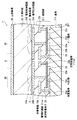
(撮像部11)
図2は、撮像部11の断面構成を隣接する2つの画素について表したものである。図3は、画素回路と電極レイアウトの一例を、インピーダンス制御部18および後述する列選択部17内のチャージアンプ回路171と共に例示したものである。模式的に表したものである。撮像部11は、入射した放射線に基づいて電気信号を発生させるものである。この撮像部11では、画素(撮像画素,単位画素)20が、行列状(マトリクス状)に2次元配置されており、撮像部11では、基板210上に、回路層211を介して画素電極21(第1電極)が配設されており、この画素電極21上には、複数の画素20にわたって(全画素にわたって)、半導体層25が形成されている。半導体層25上には、例えば全画素にわたって上部電極26(第2電極)が設けられている。
(Imaging unit 11)
FIG. 2 illustrates a cross-sectional configuration of the
回路層211には、例えば、TFT(Thin Film Transistor:薄膜トランジスタ)22、信号線電極22b(信号線Lsig)および保持容量素子23を含む画素回路(後述)が形成されている。
In the
TFT22は、例えばNチャネル型(N型)の電界効果型トランジスタ(FET:Field Effect Transistor)により構成されている。但し、TFT22はPチャネル型(P型)のFET等により構成されていてもよい。また、ここでは一例としてボトムゲート構造を示すが、これに限らずトップゲート構造であってもよい。
The
このTFT22のゲート(ゲート電極22a)は、読み出し制御線Lreadに接続され、ソースおよびドレインのうちの一方は、例えば信号線電極22b(信号線Lsig)に接続されている。ソースおよびドレインのうちの他方は、回路層211上に配設された画素電極21に接続されている。このTFT22のチャネル層22cには、例えば、非晶質シリコン(アモルファスシリコン)、微結晶シリコンまたは多結晶シリコン(ポリシリコン)等のシリコン系半導体が用いられている。あるいは、この他にも、酸化インジウムガリウム亜鉛(InGaZnO)または酸化亜鉛(ZnO)等の酸化物半導体が用いられてもよい。
The gate (
信号線電極22bは、回路層211内の画素電極21と非対向の領域に(画素電極21とオーバーラップしないように)設けられている。画素電極21との間に容量結合を生じにくくするためである。例えば、信号線電極22bは、画素間(画素電極21間)の領域Aに、例えばV方向に沿って延在してストライプ状に設けられている。
The
保持容量素子23は、層間絶縁膜211aの一部を挟んで設けられた一対の容量電極23a,23bにより形成されており、画素電極21を介して収集された信号電荷を一時的に蓄積させるものである。容量電極23a,23bのうち、容量電極23aは、例えばTFT22のゲート電極22aと同層に設けられ、容量電極23bは、例えば信号線電極22bと同層に設けられている。また、容量電極23bは、信号線電極22bと同様、画素間の領域Aに、例えばV方向に沿って延在してストライプ状に設けられている。
The
画素電極21は、半導体層25において発生したホール・電子対のうち、例えば電子を信号電荷として取り出すための電極として機能するものであり、画素毎に分離されて回路層211上に設けられている。この画素電極21は、例えばITO(インジウム錫酸化物)等から構成されている。
The
半導体層25は、入射した放射線を電気信号に変換する半導体よりなる。このような半導体としては、例えば、アモルファスセレン(a−Se)等のアモルファス半導体が挙げられる。但し、この他にも、カドミニウムテルル(CdTe)半導体等により構成されていてもよい。
The
上部電極26は、全画素に共通の電極として設けられ、半導体層25内のホール・電子対のうちのもう一方の電荷(例えばホール)を排出するための電極として機能するものである。この上部電極26は、例えばAu等から構成されている。
The
本実施の形態では、上記のような回路層211と半導体層25との間の画素電極21に非対向な領域に、画素電極21とは電気的に独立した電極(電荷制御電極24A,24B)が設けられている。具体的には、電荷制御電極24A,24B(第3電極)は、画素20間(画素電極21間)の領域Aにおいて、画素電極21と同層に設けられている。
In the present embodiment, electrodes that are electrically independent from the pixel electrode 21 (
電荷制御電極24A,24Bはそれぞれ、TFT32A,32Bおよび制御線L1を介してインピーダンス制御部18に接続されている。TFT32A,32Bは、上記TFT22と同様、電界効果型の薄膜トランジスタであり、撮像部11内に電荷制御電極24A,24Bと同一の個数設けられている。これらのTFT32A,32Bは、ゲートが制御線L1、ソースおよびドレインのうちの一方が、電荷制御電極24A,24Bに接続され、他方が所定の電位(例えばグランド電位)に保持されている。インピーダンス制御部18の駆動により、TFT32A,32Bの各ゲートには、所定の電圧パルスが印加され、TFT32A,32Bのオン動作およびオフ動作の切り替え制御がなされる。これにより、電荷制御電極24A,24Bのインピーダンスの高低が所定のタイミングで切り替えられる。このような電荷制御電極24A,24Bは、例えば画素電極21と同一の材料により構成されている。
The
これらの電荷制御電極24A,24Bのうち、電荷制御電極24Aは、信号線電極22bに対向する領域に設けられ、電荷制御電極24Bは、保持容量素子23に対向する領域に設けられている。例えば、電荷制御電極24Aは、信号線電極22bに重畳して、V方向に沿ってストライプ状に設けられ、電荷制御電極24Bは、容量電極23bに重畳してV方向に沿ってストライプ状に設けられている。画素20間の領域Aにおいては、例えば、信号線電極22bと容量電極23bとが互いに並行して配設されるが、本実施の形態のように、信号線電極22bと容量電極23bとに対向する各領域に、電荷制御電極24A,24Bを電気的に独立させて設けることが望ましい。電荷制御電極24A,24Bを電気的に分離することにより、容量結合による信号線電極22bへの電気的な影響を抑制できるためである。
Of these
(行走査部13)
行走査部13は、図示しないシフトレジスタ回路や論理回路等を含んで構成されており、撮像部11内の複数の画素20に対して行単位(水平ライン単位)での駆動(線順次走査)を行う画素駆動部(行走査回路)である。具体的には、後述する読み出し動作等の撮像動作を例えば線順次走査により行う。尚、この線順次走査は、読み出し制御線Lreadを介して前述した行走査信号を各画素20へ供給することによって行われるようになっている。
(Row scanning unit 13)
The
(A/D変換部14)
A/D変換部14は、複数(ここでは4つ)の信号線Lsigごとに1つ設けられた複数の列選択部17を有しており、信号線Lsigを介して入力した信号電圧(信号電荷)に基づいてA/D変換(アナログ/デジタル変換)を行うものである。これにより、デジタル信号からなる出力データDout(撮像信号)が生成され、外部へ出力されるようになっている。
(A / D converter 14)
The A / D conversion unit 14 includes a plurality of
列選択部17は、例えば図4に示したように、チャージアンプ回路171と、サンプルホールド(S/H)回路173、4つのスイッチSW2を含むマルチプレクサ回路(選択回路)174、およびA/Dコンバータ175を有している。これらのうち、チャージアンプ回路171、S/H回路173およびスイッチSW2はそれぞれ、信号線Lsig毎に設けられている。マルチプレクサ回路174およびA/Dコンバータ175は、列選択部17毎に設けられている。
For example, as shown in FIG. 4, the
チャージアンプ回路171は、チャージアンプ172および容量素子(コンデンサ,フィードバック容量素子)C1を含んで構成されている。チャージアンプ172は、信号線Lsigから読み出された信号電荷を電圧に変換(Q−V変換)するためのアンプ(増幅器)である。
The
S/H回路173は、チャージアンプ172とマルチプレクサ回路174(スイッチSW2)との間に配置されており、チャージアンプ172からの出力電圧Vcaを一時的に保持するための回路である。
The S /
マルチプレクサ回路174は、列走査部15による走査駆動に従って4つのスイッチSW2のうちの1つが順次オン状態となることにより、各S/H回路173とA/Dコンバータ175との間を選択的に接続または遮断する回路である。
The multiplexer circuit 174 selectively connects each S /
A/Dコンバータ175は、スイッチSW2を介して入力されたS/H回路173からの出力電圧に対してA/D変換を行うことにより、上記した出力データDoutを生成して出力する回路である。
The A /
(列走査部15)
列走査部15は、例えば図示しないシフトレジスタやアドレスデコーダ等を含んで構成されており、上記した列選択部17内の各スイッチSW2を走査しつつ順番に駆動するものである。このような列走査部15による選択走査によって、信号線Lsigの各々を介して読み出された各画素20の信号(上記した出力データDout)が、順番に外部へ出力されるようになっている。
(Column scanning unit 15)
The
(インピーダンス制御部18)
インピーダンス制御部18は、図示しない論理回路等を含んで構成されており、撮像部11内の複数の電荷制御電極24A,24Bを電圧制御し、電荷制御電極24A,24Bのインピーダンスの高低を制御するものである。このインピーダンス制御部18には、少なくとも1本の制御線L1が接続されていればよく、この1本の制御線L1が、TFT32A,32Bを介して各電荷制御電極24A,24Bに接続されている。これにより、インピーダンス制御部18は、撮像部11内に設けられた電荷制御電極24A,24Bの全てを一括して電圧制御する。
(Impedance control unit 18)
The
(システム制御部16)
システム制御部16は、行走査部13、A/D変換部14、列走査部15およびインピーダンス制御部18の動作を制御するものである。具体的には、システム制御部16は、前述した各種のタイミング信号(制御信号)を生成するタイミングジェネレータを有しており、このタイミングジェネレータにおいて生成される各種のタイミング信号を基に、行走査部13、A/D変換部14、列走査部15およびインピーダンス制御部18の駆動制御を行う。詳細は後述するが、撮影時には、このシステム制御部16の制御に基づいて、行走査部13、A/D変換部14および列走査部15が各画素20の撮像駆動を行うと共に、インピーダンス制御部18が電荷制御電極24A,24Bの電圧制御を行うようになっている。
(System control unit 16)
The
[作用、効果]
本実施の形態の撮像装置1では、放射線が撮像部11へ入射すると、各画素20内の半導体層25において、この放射線が信号電荷に変換される(半導体層25において放射線に基づく信号電荷が発生する)。詳細には、放射線照射時には、半導体層25内に、入射した放射線量に応じたホールおよび電子の対が発生する。この際、上部電極26へ所定のバイアス電圧(マイナス電圧)が印加されることにより、例えば信号電荷としての電子が画素電極21側、ホールが上部電極26側へそれぞれ移動する。これらのうち信号電荷は、画素電極21を通じて保持容量素子23に蓄積された後、読み出し動作時にTFT22がオン状態となることによって信号線Lsigへ読み出される。読み出された信号電荷は、Q−V変換およびA/D変換がなされた後、外部へ出力される。以下、この撮像駆動動作について詳細に説明する。
[Action, effect]
In the
図5(A),(B)は、撮像駆動動作の一例を説明するための模式図である。図6は、放射線(ここではX線)の照射期間(照射期間Tex)における画素20および列選択部17内のチャージアンプ回路171の動作例を表したものである。図7は、読み出し期間(読出し期間Tr)における画素20および列選択部17内のチャージアンプ回路171の動作例を表したものである。尚、図6および図7では説明の便宜上、TFT22,32A,32Bのオン・オフ状態を、スイッチを用いて表している。
5A and 5B are schematic diagrams for explaining an example of the imaging drive operation. FIG. 6 illustrates an operation example of the
図5(A)に示したように、撮像装置1では、放射線の照射期間Tex後の読み出し期間Trにおいて、撮像部11内の各画素20に対して線順次的に信号電荷の読み出しがなされる。尚、読み出し期間Trにおける矢印は、画面上部の画素から下部の画素に向かって線順次に読み出し動作がなされることを表しており、画面全体の読み出しに要する期間を「読み出し期間」とする。
As shown in FIG. 5A, in the
本実施の形態では、図5(B)に示したように、このような線順次撮像駆動と共に、電荷制御電極24A,24Bが電圧制御され、電荷制御電極24A,24Bのインピーダンスの高低が切り替えられる。具体的には、照射期間Texでは低インピーダンス(Low-Z)、読み出し期間Trでは高インピーダンス(High-Z)となるような電圧制御がなされる。
In the present embodiment, as shown in FIG. 5B, with such line-sequential imaging drive, the
詳細には、照射期間Texでは、図6に示したように、TFT22はオフ状態となっている。この状態では、画素20内の半導体層25へ入射した放射線に基づく信号電荷は、信号線Lsig側へは出力されず(読み出されず)、保持容量素子23に蓄積される。この照射期間Texでは、制御線L1を介して、TFT32A,32Bにはオン電圧(High側電圧パルス)が印加され、TFT32A,32Bがオン状態となる。これにより、電荷制御電極24A,24Bは電圧印加状態に保持され、低インピーダンスとなる。
Specifically, in the irradiation period Tex, as shown in FIG. 6, the
この後、読み出し期間Trでは、図7に示したように、TFT22がオン状態となることにより、保持容量素子23から信号線Lsig側へ信号電荷が読み出される。この読み出し期間Trでは、制御線L1を介してTFT32A,32Bにはオフ電圧(Low側電圧パルス)が印加され、TFT32A,32Bがオフ状態となる。これにより、電荷制御電極24A,24Bは電圧無印加状態(フローティング状態)に保持され、高インピーダンスとなる。
Thereafter, in the readout period Tr, as shown in FIG. 7, the
このようにして読み出された信号電荷は、チャージアンプ回路171へ入力される。詳細には、読み出された信号電荷は、信号線Lsigを介して複数(ここでは4つ)の画素列ごとに、A/D変換部14内の列選択部17へ入力される。列選択部17では、まず、信号線Lsig毎に、入力された信号電荷がチャージアンプ回路171においてQ−V変換(信号電荷から信号電圧への変換)される。次いで、変換後の信号電圧は、S/H回路173およびマルチプレクサ回路174を介してA/Dコンバータ175においてA/D変換される。このようにして、デジタル信号からなる出力データDout(撮像信号)が生成され、各列選択部17から出力される。出力データDoutは、外部へ伝送されるか、あるいは図示しない内部メモリーに記憶される。以上のようにして、撮像装置1では、撮像駆動動作がなされる。
The signal charge read in this way is input to the
(比較例)
ここで、図8に、比較例に係る撮像装置の照射期間Texにおける画素内の電荷の挙動について示す。この比較例の撮像装置は、本実施の形態と同様、各画素において、基板101上に、TFT106、信号線電極106bおよび保持容量素子107を含む回路層102が設けられ、この回路層102上に画素電極103が配設されている。画素電極103上には、全画素にわたって半導体層104が形成され、この半導体層104上に上部電極105が設けられている。但し、比較例では、画素間の領域(信号線電極106bおよび保持容量素子107に対向する領域)には、画素電極103の形成されていない領域(画素電極103に非対向の領域)Bが存在する。
(Comparative example)
Here, FIG. 8 shows the behavior of the charge in the pixel in the irradiation period Tex of the imaging apparatus according to the comparative example. In the imaging device of this comparative example, as in this embodiment, in each pixel, a
この比較例においても、本実施の形態と同様、照射期間Texには、放射線に基づいて発生したホール(図中「h」で示す)および電子(図中「e」で示す)の対のうち、信号電荷としての電子が、画素電極103側に、ホールは上部電極105側にそれぞれ移動し、信号電荷は保持容量素子107に蓄積される。そして、読み出し期間Trでは、この保持容量素子107に蓄積された信号電荷が図示しない信号線へ読み出される。ところが、各画素の半導体層104のうちの領域Bでは、画素電極103に対向する領域に比べて電界が弱いことから、読み出し動作後においても半導体層104内に信号電荷が残存してしまう(図中のB1)。
Also in this comparative example, as in the present embodiment, during the irradiation period Tex, a pair of holes (indicated by “h” in the figure) and electrons (indicated by “e” in the figure) generated based on radiation is included. Electrons as signal charges move to the
これに対し、本実施の形態では、半導体層25と回路層211との間の画素電極21に非対向な領域(画素間の領域A)に、インピーダンス制御部18によって電圧制御される電荷制御電極24A,24Bが設けられている。具体的には、電荷制御電極24A,24Bのインピーダンスの高低を所定のタイミングで切り替えるような電圧制御がなされる(照射期間Texには低インピーダンス、読み出し期間Trには高インピーダンスとなるような制御がなされる)。
In contrast, in the present embodiment, a charge control electrode that is voltage-controlled by the
上記のように、照射期間Texにおいて、電荷制御電極24A,24Bを低インピーダンスに保持することにより、画素間の領域Aにも電界が印加される。この領域Aにおいて発生したホール・電子対のうちの一方は、上部電極26側へ移動し、他方は電荷制御電極24A,24B側へ移動する。これにより、電荷制御電極24A,24Bを通じて電荷が画素20の外部へ排出される(図9)。一方、半導体層25内において発生したホールは、上部電極26を通じて画素20の外部へ排出される。尚、このような電荷制御電極24A,24Bからの電荷排出は、照射期間Tex(低インピーダンスに保持されている期間)中、継続してなされる。これにより、領域Aにおける信号電荷の残存が抑制される。また、読み出し期間Trにおいて、電荷制御電極24A,24Bを高インピーダンスに保持する(電荷制御電極24A,24Bをフローティング状態とする)ことにより、電荷制御電極24A,24Bの容量が減少して、信号線電極22bとの容量結合が軽減する。
As described above, an electric field is also applied to the region A between the pixels by holding the
以上のように本実施の形態では、各画素20の半導体層25に放射線が入射すると、半導体層25において信号電荷が発生し、画素20内に蓄積される。各画素20から蓄積された信号電荷を読み出すことにより、放射線に基づく撮像画像を得ることができる。回路層211と半導体層25との間の画素電極21に非対向な領域(領域A)に電荷制御電極24A,24Bを設け、この電荷制御電極24A,24Bを電圧制御する。これにより、半導体層25のうちの特に画素電極21間の領域等、電界が及びにくい領域における信号電荷の残存を抑制できる。よって、信号電荷の残存によるノイズの発生を抑制して、撮像画像の高画質化を実現することが可能となる。
As described above, in the present embodiment, when radiation is incident on the
具体的には、照射期間Texでは電荷制御電極24A,24Bを低インピーダンスとし、読み出し期間Trでは電荷制御電極24A,24Bを高インピーダンスとすることにより、効率的に照射期間Tex中には信号電荷を溜めつつも、読み出し期間Tr後には半導体層25内に信号電荷を残存させないように制御することができる。
Specifically, the
また、読み出し期間Trにおいて、電荷制御電極24Aを高インピーダンスとすることにより、信号線電極22bと電荷制御電極24A,24Bとの容量結合を軽減できる。電荷制御電極24Aは、領域Aにおいて信号線電極22bに対向配置されることから容量結合による読み出し速度の低下が懸念されるが、本実施の形態のように読み出し期間Trに電荷制御電極24Aが高インピーダンスであれば、電荷制御電極24A,24Bの容量が減少して、読み出し速度の低下を抑制できる。加えて、これにより、信号線電極22bおよび保持容量素子23に重畳して、電荷制御電極24A,24Bを配置できることから、画素電極の面積を縮小したり、画素間に別途電極設置スペースを設ける必要がなく、開口率への影響が少ない。
Further, by setting the
次に、上記実施の形態の撮像装置の変形例について説明する。尚、上記実施の形態と同様の構成要素については同一の符号を付し、その説明を省略する。 Next, a modification of the imaging device according to the above embodiment will be described. In addition, the same code | symbol is attached | subjected about the component similar to the said embodiment, and the description is abbreviate | omitted.
<変形例>
図10は、変形例に係る撮像装置の電荷制御電極24A,24Bに対する電圧制御動作について説明するための模式図である。本変形例においても、上記実施の形態と同様、半導体層25と回路層211との間の画素電極21に非対向な領域に、電荷制御電極24A,24Bが設けられている。また、撮像駆動動作の際には、照射期間Texにおいて電荷制御電極24Aを低インピーダンス、読み出し期間Trにおいて電荷制御電極24Bを高インピーダンスとなるようにインピーダンスの高低を切り替える制御を行う。
<Modification>
FIG. 10 is a schematic diagram for explaining a voltage control operation for the
但し、本変形例では、照射期間Texにおいて、電荷制御電極24Aを低インピーダンスに保持する際に、信号電荷が図10に示したような挙動を示すような電圧制御を行う。即ち、電荷制御電極24A,24Bを所定の電圧印加状態に保持して、半導体層25のうちの領域Aにおいて発生した信号電荷を、画素電極21へ向かって移動させるような電界を形成する。具体的には、上部電極26にバイアス電圧(マイナス電圧)を印加し、電荷制御電極24A,24Bへの印加電圧を、画素電極21への印加電圧よりも低く設定する。
これにより、半導体層25内において発生した信号電荷は、画素電極21へ向けて集まり易くなる。従って、信号電荷が領域Aに溜まりにくくなり、画素電極21からの電荷収集効率も高まる。
However, in this modification, voltage control is performed so that the signal charge behaves as shown in FIG. 10 when the
As a result, signal charges generated in the
上記の実施の形態および変形例に係る撮像装置では、入射した放射線に基づいて電気信号を得る、様々な種類の放射線撮像装置として利用される。放射線撮像装置としては、例えば、医療用のX線撮像装置(Digital Radiography等)や、空港等で用いられる携帯物検査用X線撮影装置、工業用X線撮像装置(例えば、コンテナ内の危険物等の検査や、鞄等の中身の検査を行う装置)などに適用することが可能である。 The imaging devices according to the above-described embodiments and modifications are used as various types of radiation imaging devices that obtain an electrical signal based on incident radiation. Examples of the radiation imaging apparatus include a medical X-ray imaging apparatus (Digital Radiography, etc.), a portable object inspection X-ray imaging apparatus used in an airport, etc., an industrial X-ray imaging apparatus (for example, a dangerous substance in a container) It is possible to apply to the inspection etc. of the etc., the apparatus which inspects the contents of a bag etc.).
<適用例>
続いて、上記実施の形態および変形例に係る撮像装置は、以下に説明するような撮像表示システムへ適用可能である。
<Application example>
Subsequently, the imaging apparatus according to the above-described embodiment and modification examples can be applied to an imaging display system as described below.
図11は、適用例に係る撮像表示システム(撮像表示システム5)の概略構成例を模式的に表したものである。撮像表示システム5は、上述の撮像部11を有する撮像装置1と、画像処理部52と、表示装置4とを備えており、この例では放射線を用いた撮像表示システム(放射線撮像表示システム)である。
FIG. 11 schematically illustrates a schematic configuration example of an imaging display system (imaging display system 5) according to an application example. The imaging display system 5 includes the
画像処理部52は、撮像装置1から出力される出力データDout(撮像信号)に対して所定の画像処理を施すことにより、画像データD1を生成するものである。表示装置4は、画像処理部52において生成された画像データD1に基づく画像表示を、所定のモニタ画面40上で行うものである。
The
この撮像表示システム5では、撮像装置1(ここでは放射線撮像装置)が、光源(ここではX線源等の放射線源)51から被写体50に向けて照射された照射光(ここでは放射線)に基づき、被写体50の画像データDoutを取得し、画像処理部52へ出力する。画像処理部52は、入力された画像データDoutに対して上記した所定の画像処理を施し、その画像処理後の画像データ(表示データ)D1を表示装置4へ出力する。表示装置4は、入力された画像データD1に基づいて、モニタ画面40上に画像情報(撮像画像)を表示する。
In this imaging display system 5, the imaging device 1 (here, a radiation imaging device) is based on irradiation light (here, radiation) emitted from a light source (here, a radiation source such as an X-ray source) 51 toward a subject 50. The image data Dout of the subject 50 is acquired and output to the
このように、本適用例の撮像表示システム5では、撮像装置1において被写体50の画像を電気信号として取得可能であるため、取得した電気信号を表示装置4へ伝送することによって画像表示を行うことができる。即ち、従来のような放射線写真フィルムを用いることなく、被写体50の画像を観察することが可能となり、また、動画撮影および動画表示にも対応可能となる。
As described above, in the imaging display system 5 of this application example, the image of the subject 50 can be acquired as an electrical signal in the
尚、本適用例では、撮像装置1が放射線撮像装置として構成されており、放射線を用いた撮像表示システムとなっている場合を例に挙げて説明したが、本開示の撮像表示システムは、他の方式の撮像装置を用いたものにも適用することが可能である。
In this application example, the case where the
以上、実施の形態、変形例および適用例を挙げたが、本開示内容はこれらの実施の形態等に限定されず、種々の変形が可能である。例えば、撮像部における画素の回路構成は、上記実施の形態等で説明したもの(画素20,20A〜20Dの回路構成)には限られず、他の回路構成であってもよい。同様に、行走査部や列選択部等の回路構成についても、上記実施の形態等で説明したものには限られず、他の回路構成であってもよい。
As mentioned above, although embodiment, the modification, and the application example were mentioned, this indication content is not limited to these embodiment etc., A various deformation | transformation is possible. For example, the circuit configuration of the pixel in the imaging unit is not limited to the one described in the above embodiment and the like (the circuit configuration of the
また、上記実施の形態等で説明した撮像部、行走査部、A/D変換部(列選択部)および列走査部等はそれぞれ、例えば同一基板上に形成されているようにしてもよい。具体的には、例えば低温多結晶シリコンなどの多結晶半導体を用いることにより、これらの回路部分におけるスイッチ等も同一基板上に形成することができるようになる。このため、例えば外部のシステム制御部からの制御信号に基づいて、同一基板上における駆動動作を行うことが可能となり、狭額縁化(3辺フリーの額縁構造)や配線接続の際の信頼性向上を実現することができる。 Further, the imaging unit, the row scanning unit, the A / D conversion unit (column selection unit), the column scanning unit, and the like described in the above embodiments may be formed on the same substrate, for example. Specifically, by using a polycrystalline semiconductor such as low-temperature polycrystalline silicon, switches and the like in these circuit portions can be formed on the same substrate. For this reason, for example, it becomes possible to perform a driving operation on the same substrate based on a control signal from an external system control unit, and to improve reliability when narrowing the frame (three-side free frame structure) or wiring connection. Can be realized.
更に、上記実施の形態等では、電荷制御電極24A,24Bが画素間の領域AにV方向に沿ったストライプ状に設けられた構成を例に挙げて説明したが、電荷制御電極24A,24Bの平面形状および設置領域はこれに限定されるものではない。例えば、H方向に沿ったストライプ状に設けられていてもよいし、あるいは画素電極21の周縁を囲うように(全体として格子状に)設けられていてもよい。
Further, in the above-described embodiment and the like, the
加えて、上記実施の形態等では、信号線電極22bに対向して電荷制御電極24Aを、保持容量素子23に対向して電荷制御電極24Bをそれぞれ電気的に独立させて配置した構成を例示したが、これらの電荷制御電極24A,24Bは一体的に設けられていてもよい。即ち、領域Aにおいて、信号線電極22bと保持容量素子23(容量電極23b)とが互いに並行して配置されている場合には、これらの信号線電極22bと保持容量素子23の双方に対向する1本の電荷制御電極を設けるようにしてもよい。但し、信号線電極22bとの容量結合を考慮すると、上記実施の形態において説明したように、電荷制御電極24A,24Bを電気的に分離して設けることが望ましい。
In addition, in the above-described embodiment and the like, the configuration in which the
尚、本開示は以下のような構成であってもよい。
(1)
複数の画素を有する撮像部と、
前記複数の画素のそれぞれに蓄積された信号電荷の読み出しを行う駆動部とを備え、
各画素は、
電界効果型トランジスタ、信号線および保持容量素子を含む回路層と、
前記回路層上に前記画素毎に配設された第1電極と、
前記第1電極上に前記複数の画素にわたって形成されると共に、入射した放射線に基づいて信号電荷を発生させる半導体層と、
前記半導体層上に設けられた第2電極と、
前記回路層と前記半導体層との間の前記第1電極に非対向な領域に配置され、前記駆動部により電圧制御される第3電極とを有する
撮像装置。
(2)
前記駆動部は、前記第3電極を電圧制御して、前記第3電極のインピーダンスの高低を切り替える
上記(1)に記載の撮像装置。
(3)
前記駆動部は、前記第3電極の前記信号電荷の読み出し期間におけるインピーダンスが、前記放射線の照射期間におけるインピーダンスよりも高くなるように、前記第3電極を電圧制御する
上記(2)に記載の撮像装置。
(4)
前記駆動部は、前記第3電極を、前記読み出し期間には電圧無印加状態に保持し、前記照射期間には電圧印加状態に保持する
上記(3)に記載の撮像装置。
(5)
前記駆動部は、前記照射期間において、前記半導体層のうちの前記第3電極に対向する領域内で生じた前記信号電荷が前記第1電極へ向かって移動するように、前記第3電極を電圧制御する
上記(4)に記載の撮像装置。
(6)
前記第3電極は、前記第1電極と同層に配置されている
上記(1)〜(5)のいずれかに記載の撮像装置。
(7)
前記第3電極は、画素間の領域に設けられている
上記(1)〜(5)のいずれかに記載の撮像装置。
(8)
前記複数の画素はマトリクス状に2次元配置され、
前記第3電極は、前記画素の配列方向に沿ってストライプ状に設けられている
上記(7)に記載の撮像装置。
(9)
前記第3電極は、前記信号線および前記保持容量素子に対向して配置されている
上記(1)〜(8)のいずれかに記載の撮像装置。
(10)
前記放射線はX線である
上記(1)〜(9)のいずれかに記載の撮像装置。
(11)
撮像装置と、この撮像装置により得られた撮像信号に基づく画像表示を行う表示装置とを備え
前記撮像装置は、
各々が光電変換素子を含む複数の画素を有する撮像部と、
前記複数の画素のそれぞれに蓄積された信号電荷の読み出しを行う駆動部とを備え、
各画素は、
電界効果型トランジスタ、信号線および保持容量素子を含む回路層と、
前記回路層上に前記画素毎に配設された第1電極と、
前記第1電極上に前記複数の画素にわたって形成されると共に、入射した放射線に基づいて信号電荷を発生させる半導体層と、
前記半導体層上に設けられた第2電極と、
前記回路層と前記半導体層との間の前記第1電極に非対向な領域に配置され、前記駆動部により電圧制御される第3電極とを有する
撮像表示システム。
The present disclosure may be configured as follows.
(1)
An imaging unit having a plurality of pixels;
A drive unit that reads out signal charges accumulated in each of the plurality of pixels,
Each pixel is
A circuit layer including a field effect transistor, a signal line, and a storage capacitor;
A first electrode disposed for each pixel on the circuit layer;
A semiconductor layer formed over the plurality of pixels on the first electrode and generating a signal charge based on incident radiation;
A second electrode provided on the semiconductor layer;
An imaging apparatus comprising: a third electrode disposed in a region not facing the first electrode between the circuit layer and the semiconductor layer, the voltage of which is controlled by the driving unit.
(2)
The imaging device according to (1), wherein the driving unit switches the level of the impedance of the third electrode by controlling the voltage of the third electrode.
(3)
The imaging unit according to (2), wherein the driving unit voltage-controls the third electrode such that an impedance of the third electrode in the signal charge readout period is higher than an impedance in the radiation irradiation period. apparatus.
(4)
The imaging device according to (3), wherein the driving unit holds the third electrode in a voltage non-application state during the readout period and holds a voltage application state during the irradiation period.
(5)
The driving unit applies a voltage to the third electrode so that the signal charge generated in a region of the semiconductor layer facing the third electrode moves toward the first electrode during the irradiation period. The imaging device according to (4), which is controlled.
(6)
The imaging device according to any one of (1) to (5), wherein the third electrode is disposed in the same layer as the first electrode.
(7)
The imaging device according to any one of (1) to (5), wherein the third electrode is provided in a region between pixels.
(8)
The plurality of pixels are two-dimensionally arranged in a matrix,
The imaging device according to (7), wherein the third electrode is provided in a stripe shape along an arrangement direction of the pixels.
(9)
The imaging device according to any one of (1) to (8), wherein the third electrode is disposed to face the signal line and the storage capacitor element.
(10)
The imaging device according to any one of (1) to (9), wherein the radiation is X-rays.
(11)
An imaging device, and a display device that displays an image based on an imaging signal obtained by the imaging device.
An imaging unit having a plurality of pixels each including a photoelectric conversion element;
A drive unit that reads out signal charges accumulated in each of the plurality of pixels,
Each pixel is
A circuit layer including a field effect transistor, a signal line, and a storage capacitor;
A first electrode disposed for each pixel on the circuit layer;
A semiconductor layer formed over the plurality of pixels on the first electrode and generating a signal charge based on incident radiation;
A second electrode provided on the semiconductor layer;
An imaging display system comprising: a third electrode disposed in a region not facing the first electrode between the circuit layer and the semiconductor layer, the voltage of which is controlled by the driving unit.
1…撮像装置、11…撮像部、13…行走査部、14…A/D変換部、15…列走査部、16…システム制御部、17…列選択部、171…チャージアンプ回路、172…チャージアンプ、173…S/H回路、174…マルチプレクサ回路、175…A/Dコンバータ、18…インピーダンス制御部、20…画素(撮像画素)、21…画素電極、22…TFT、22a…ゲート電極、22b…信号線電極、22c…チャネル層、23…保持容量素子、23a,23b…容量電極、24A,24B…電荷制御電極、25…半導体層、26…上部電極、4…表示装置、40…モニタ画面、5…撮像表示システム、50…被写体、51…放射線源、52…画像処理部、Lsig…信号線、Lread…読み出し制御線、Dout…出力データ、D1…撮像信号、Tex…照射期間、Tr…読み出し期間。
DESCRIPTION OF
Claims (11)
前記複数の画素のそれぞれに蓄積された信号電荷の読み出しを行う駆動部とを備え、
各画素は、
電界効果型トランジスタ、信号線および保持容量素子を含む回路層と、
前記回路層上に前記画素毎に配設された第1電極と、
前記第1電極上に前記複数の画素にわたって形成されると共に、入射した放射線に基づいて信号電荷を発生させる半導体層と、
前記半導体層上に設けられた第2電極と、
前記回路層と前記半導体層との間の前記第1電極に非対向な領域に配置され、前記駆動部により電圧制御される第3電極とを有する
撮像装置。 An imaging unit having a plurality of pixels;
A drive unit that reads out signal charges accumulated in each of the plurality of pixels,
Each pixel is
A circuit layer including a field effect transistor, a signal line, and a storage capacitor;
A first electrode disposed for each pixel on the circuit layer;
A semiconductor layer formed over the plurality of pixels on the first electrode and generating a signal charge based on incident radiation;
A second electrode provided on the semiconductor layer;
An imaging apparatus comprising: a third electrode disposed in a region not facing the first electrode between the circuit layer and the semiconductor layer, the voltage of which is controlled by the driving unit.
請求項1に記載の撮像装置。 The imaging apparatus according to claim 1, wherein the driving unit switches the level of the impedance of the third electrode by controlling the voltage of the third electrode.
請求項2に記載の撮像装置。 The imaging device according to claim 2, wherein the driving unit voltage-controls the third electrode so that an impedance of the third electrode in the signal charge readout period is higher than an impedance in the radiation irradiation period. .
請求項3に記載の撮像装置。 The imaging device according to claim 3, wherein the driving unit holds the third electrode in a voltage non-application state during the readout period and holds a voltage application state during the irradiation period.
請求項4に記載の撮像装置。 The driving unit applies a voltage to the third electrode so that the signal charge generated in a region of the semiconductor layer facing the third electrode moves toward the first electrode during the irradiation period. The imaging device according to claim 4 to be controlled.
請求項1に記載の撮像装置。 The imaging device according to claim 1, wherein the third electrode is disposed in the same layer as the first electrode.
請求項1に記載の撮像装置。 The imaging device according to claim 1, wherein the third electrode is provided in a region between pixels.
前記第3電極は、前記画素の配列方向に沿ってストライプ状に設けられている
請求項7に記載の撮像装置。 The plurality of pixels are two-dimensionally arranged in a matrix,
The imaging device according to claim 7, wherein the third electrode is provided in a stripe shape along the arrangement direction of the pixels.
請求項1に記載の撮像装置。 The imaging device according to claim 1, wherein the third electrode is disposed to face the signal line and the storage capacitor element.
請求項1に記載の撮像装置。 The imaging device according to claim 1, wherein the radiation is X-rays.
前記撮像装置は、
複数の画素を有する撮像部と、
前記複数の画素のそれぞれに蓄積された信号電荷の読み出しを行う駆動部とを備え、
各画素は、
電界効果型トランジスタ、信号線および保持容量素子を含む回路層と、
前記回路層上に前記画素毎に配設された第1電極と、
前記第1電極上に前記複数の画素にわたって形成されると共に、入射した放射線に基づいて信号電荷を発生させる半導体層と、
前記半導体層上に設けられた第2電極と、
前記回路層と前記半導体層との間の前記第1電極に非対向な領域に配置され、前記駆動部により電圧制御される第3電極とを有する
撮像表示システム。 An imaging device, and a display device that displays an image based on an imaging signal obtained by the imaging device.
An imaging unit having pixels of multiple,
A drive unit that reads out signal charges accumulated in each of the plurality of pixels,
Each pixel is
A circuit layer including a field effect transistor, a signal line, and a storage capacitor;
A first electrode disposed for each pixel on the circuit layer;
A semiconductor layer formed over the plurality of pixels on the first electrode and generating a signal charge based on incident radiation;
A second electrode provided on the semiconductor layer;
An imaging display system comprising: a third electrode disposed in a region not facing the first electrode between the circuit layer and the semiconductor layer, the voltage of which is controlled by the driving unit.
Priority Applications (3)
| Application Number | Priority Date | Filing Date | Title |
|---|---|---|---|
| JP2012072895A JP5895650B2 (en) | 2012-03-28 | 2012-03-28 | Imaging apparatus and imaging display system |
| US13/777,250 US8952336B2 (en) | 2012-03-28 | 2013-02-26 | Image pickup device and image pickup display system |
| CN201310091011.0A CN103369258B (en) | 2012-03-28 | 2013-03-21 | Image pick-up device and image pickup show system |
Applications Claiming Priority (1)
| Application Number | Priority Date | Filing Date | Title |
|---|---|---|---|
| JP2012072895A JP5895650B2 (en) | 2012-03-28 | 2012-03-28 | Imaging apparatus and imaging display system |
Publications (3)
| Publication Number | Publication Date |
|---|---|
| JP2013205140A JP2013205140A (en) | 2013-10-07 |
| JP2013205140A5 JP2013205140A5 (en) | 2015-04-02 |
| JP5895650B2 true JP5895650B2 (en) | 2016-03-30 |
Family
ID=49233621
Family Applications (1)
| Application Number | Title | Priority Date | Filing Date |
|---|---|---|---|
| JP2012072895A Expired - Fee Related JP5895650B2 (en) | 2012-03-28 | 2012-03-28 | Imaging apparatus and imaging display system |
Country Status (3)
| Country | Link |
|---|---|
| US (1) | US8952336B2 (en) |
| JP (1) | JP5895650B2 (en) |
| CN (1) | CN103369258B (en) |
Families Citing this family (8)
| Publication number | Priority date | Publication date | Assignee | Title |
|---|---|---|---|---|
| JP5895504B2 (en) | 2011-12-15 | 2016-03-30 | ソニー株式会社 | Imaging panel and imaging processing system |
| CN105453269B (en) * | 2013-08-07 | 2019-04-05 | 夏普株式会社 | Radioscopic image sensor substrate |
| JP6555867B2 (en) | 2014-09-26 | 2019-08-07 | キヤノン株式会社 | Imaging device |
| JP6512909B2 (en) | 2015-04-09 | 2019-05-15 | キヤノン株式会社 | Radiation imaging apparatus and radiation imaging system |
| DE102016122658B4 (en) | 2015-12-04 | 2021-07-15 | Canon Kabushiki Kaisha | Imaging device and system |
| JP6808316B2 (en) * | 2015-12-04 | 2021-01-06 | キヤノン株式会社 | Imaging device and imaging system |
| JP7020770B2 (en) * | 2015-12-04 | 2022-02-16 | キヤノン株式会社 | Imaging device and imaging system |
| JP2021100081A (en) * | 2019-12-23 | 2021-07-01 | 株式会社ジャパンディスプレイ | Detector |
Family Cites Families (26)
| Publication number | Priority date | Publication date | Assignee | Title |
|---|---|---|---|---|
| GB2289983B (en) * | 1994-06-01 | 1996-10-16 | Simage Oy | Imaging devices,systems and methods |
| US5591963A (en) * | 1994-08-22 | 1997-01-07 | Canon Kabushiki Kaisha | Photoelectric conversion device with dual insulating layer |
| US5677539A (en) * | 1995-10-13 | 1997-10-14 | Digirad | Semiconductor radiation detector with enhanced charge collection |
| DE19616545B4 (en) * | 1996-04-25 | 2006-05-11 | Siemens Ag | Fast radiation detector |
| DE69623659T2 (en) * | 1996-05-08 | 2003-05-08 | Ifire Technology Inc | HIGH-RESOLUTION FLAT SENSOR FOR RADIATION IMAGING SYSTEM |
| JPH11218858A (en) * | 1998-01-30 | 1999-08-10 | Konica Corp | Method for removing residual charge for x-ray image pickup panel |
| KR100279294B1 (en) * | 1998-05-21 | 2001-02-01 | 윤종용 | Source follower circuit having improved gain and output circuit of solid-state imaging device using the same |
| JP4188544B2 (en) * | 2000-07-03 | 2008-11-26 | 富士フイルム株式会社 | Image information recording method and apparatus, and image information reading method and apparatus |
| JP3984808B2 (en) * | 2000-09-07 | 2007-10-03 | キヤノン株式会社 | Signal processing apparatus, imaging apparatus using the same, and radiation imaging system |
| JP3678162B2 (en) | 2001-04-12 | 2005-08-03 | 株式会社島津製作所 | Radiation detector |
| JP2004071638A (en) * | 2002-08-01 | 2004-03-04 | Canon Inc | Radiation imaging apparatus and radiation imaging system using same |
| JP3757946B2 (en) * | 2003-03-18 | 2006-03-22 | 株式会社島津製作所 | Radiation imaging device |
| JP2006005057A (en) * | 2004-06-16 | 2006-01-05 | Fuji Photo Film Co Ltd | Radiation image recording medium and image display medium |
| US7304308B2 (en) * | 2005-02-16 | 2007-12-04 | Hologic, Inc. | Amorphous selenium flat panel x-ray imager for tomosynthesis and static imaging |
| US7122803B2 (en) * | 2005-02-16 | 2006-10-17 | Hologic, Inc. | Amorphous selenium flat panel x-ray imager for tomosynthesis and static imaging |
| US20070290142A1 (en) * | 2006-06-16 | 2007-12-20 | General Electeric Company | X-ray detectors with adjustable active area electrode assembly |
| US8193501B2 (en) * | 2006-07-20 | 2012-06-05 | Koninklijke Philips Electronics N.V. | Detector for and a method of detecting electromagnetic radiation |
| JP4106397B2 (en) * | 2006-09-14 | 2008-06-25 | 株式会社島津製作所 | Method for manufacturing light or radiation detector |
| JP2008089345A (en) * | 2006-09-29 | 2008-04-17 | Fujifilm Corp | Radiation conversion panel, radiation image information reading apparatus and method using it |
| US7601962B2 (en) * | 2007-01-12 | 2009-10-13 | General Electric Company | Systems and methods for reading data |
| JP5070031B2 (en) * | 2007-12-25 | 2012-11-07 | 富士フイルム株式会社 | Radiation image detector |
| JP5361267B2 (en) * | 2008-07-18 | 2013-12-04 | 富士フイルム株式会社 | Signal line correction method and apparatus |
| JP5602390B2 (en) * | 2008-08-19 | 2014-10-08 | 富士フイルム株式会社 | Thin film transistor, active matrix substrate, and imaging device |
| JP5172573B2 (en) * | 2008-09-29 | 2013-03-27 | 富士フイルム株式会社 | Afterimage correction method and apparatus |
| CA2766485C (en) * | 2009-07-16 | 2017-07-25 | Karim S. Karim | Multi-layer flat panel x-ray detector |
| JP5495711B2 (en) * | 2009-10-26 | 2014-05-21 | キヤノン株式会社 | Imaging apparatus and imaging system, control method thereof, and program thereof |
-
2012
- 2012-03-28 JP JP2012072895A patent/JP5895650B2/en not_active Expired - Fee Related
-
2013
- 2013-02-26 US US13/777,250 patent/US8952336B2/en not_active Expired - Fee Related
- 2013-03-21 CN CN201310091011.0A patent/CN103369258B/en not_active Expired - Fee Related
Also Published As
| Publication number | Publication date |
|---|---|
| US20130256544A1 (en) | 2013-10-03 |
| US8952336B2 (en) | 2015-02-10 |
| CN103369258A (en) | 2013-10-23 |
| JP2013205140A (en) | 2013-10-07 |
| CN103369258B (en) | 2017-09-08 |
Similar Documents
| Publication | Publication Date | Title |
|---|---|---|
| JP5895650B2 (en) | Imaging apparatus and imaging display system | |
| JP5874670B2 (en) | Imaging apparatus and imaging display system | |
| US9053994B2 (en) | Image pickup unit and image pickup display system | |
| JP5935287B2 (en) | Imaging apparatus and imaging display system | |
| JP5988291B2 (en) | Imaging apparatus and imaging display system | |
| JP5999921B2 (en) | Imaging apparatus and imaging display system | |
| JP5935286B2 (en) | Imaging apparatus and imaging display system | |
| JP6152729B2 (en) | Imaging apparatus and imaging display system | |
| JP5935285B2 (en) | Imaging apparatus and imaging display system | |
| JP2015023080A (en) | Radiation imaging apparatus and radiation imaging display system | |
| WO2015008630A1 (en) | Radiographic imaging device and radiographic imaging/display system | |
| JP5935291B2 (en) | Imaging apparatus and imaging display system | |
| JP5974654B2 (en) | Imaging apparatus and imaging display system | |
| JP2014192320A (en) | Imaging device and imaging display system | |
| JP2012129425A (en) | Matrix substrate, detection apparatus, detection system and detection apparatus driving method | |
| US9564461B2 (en) | Radiation image-pickup device and radiation image-pickup display system | |
| JP6190192B2 (en) | Radiation imaging apparatus and radiation imaging display system | |
| JP6166128B2 (en) | Radiation imaging apparatus and radiation imaging display system | |
| US20130075621A1 (en) | Radiation detection apparatus and detection system including same | |
| JP5817227B2 (en) | Radiation imaging apparatus and radiation imaging display system | |
| CN115808431A (en) | Dynamic X-ray detection panel, X-ray detector and method of driving the same |
Legal Events
| Date | Code | Title | Description |
|---|---|---|---|
| A521 | Request for written amendment filed |
Free format text: JAPANESE INTERMEDIATE CODE: A523 Effective date: 20150213 |
|
| A621 | Written request for application examination |
Free format text: JAPANESE INTERMEDIATE CODE: A621 Effective date: 20150213 |
|
| A977 | Report on retrieval |
Free format text: JAPANESE INTERMEDIATE CODE: A971007 Effective date: 20160120 |
|
| TRDD | Decision of grant or rejection written | ||
| A01 | Written decision to grant a patent or to grant a registration (utility model) |
Free format text: JAPANESE INTERMEDIATE CODE: A01 Effective date: 20160202 |
|
| A61 | First payment of annual fees (during grant procedure) |
Free format text: JAPANESE INTERMEDIATE CODE: A61 Effective date: 20160215 |
|
| R151 | Written notification of patent or utility model registration |
Ref document number: 5895650 Country of ref document: JP Free format text: JAPANESE INTERMEDIATE CODE: R151 |
|
| S111 | Request for change of ownership or part of ownership |
Free format text: JAPANESE INTERMEDIATE CODE: R313111 |
|
| R350 | Written notification of registration of transfer |
Free format text: JAPANESE INTERMEDIATE CODE: R350 |
|
| R250 | Receipt of annual fees |
Free format text: JAPANESE INTERMEDIATE CODE: R250 |
|
| R250 | Receipt of annual fees |
Free format text: JAPANESE INTERMEDIATE CODE: R250 |
|
| LAPS | Cancellation because of no payment of annual fees |