JP5935291B2 - Imaging apparatus and imaging display system - Google Patents
Imaging apparatus and imaging display system Download PDFInfo
- Publication number
- JP5935291B2 JP5935291B2 JP2011240135A JP2011240135A JP5935291B2 JP 5935291 B2 JP5935291 B2 JP 5935291B2 JP 2011240135 A JP2011240135 A JP 2011240135A JP 2011240135 A JP2011240135 A JP 2011240135A JP 5935291 B2 JP5935291 B2 JP 5935291B2
- Authority
- JP
- Japan
- Prior art keywords
- pixel
- period
- amplifier
- imaging
- reset operation
- Prior art date
- Legal status (The legal status is an assumption and is not a legal conclusion. Google has not performed a legal analysis and makes no representation as to the accuracy of the status listed.)
- Expired - Fee Related
Links
- 238000003384 imaging method Methods 0.000 title claims description 196
- 238000006243 chemical reaction Methods 0.000 claims description 99
- 230000005855 radiation Effects 0.000 claims description 30
- 230000035945 sensitivity Effects 0.000 claims description 3
- 230000000368 destabilizing effect Effects 0.000 claims 2
- 230000004048 modification Effects 0.000 description 35
- 238000012986 modification Methods 0.000 description 35
- 238000010586 diagram Methods 0.000 description 29
- 230000000875 corresponding effect Effects 0.000 description 7
- 230000000694 effects Effects 0.000 description 7
- 238000000034 method Methods 0.000 description 6
- 239000004065 semiconductor Substances 0.000 description 6
- 101150105133 RRAD gene Proteins 0.000 description 5
- 230000007423 decrease Effects 0.000 description 5
- 229910021420 polycrystalline silicon Inorganic materials 0.000 description 4
- XLOMVQKBTHCTTD-UHFFFAOYSA-N Zinc monoxide Chemical compound [Zn]=O XLOMVQKBTHCTTD-UHFFFAOYSA-N 0.000 description 3
- 230000001603 reducing effect Effects 0.000 description 3
- 239000000758 substrate Substances 0.000 description 3
- OAICVXFJPJFONN-UHFFFAOYSA-N Phosphorus Chemical compound [P] OAICVXFJPJFONN-UHFFFAOYSA-N 0.000 description 2
- 206010047571 Visual impairment Diseases 0.000 description 2
- 238000009825 accumulation Methods 0.000 description 2
- 229910021417 amorphous silicon Inorganic materials 0.000 description 2
- 230000003321 amplification Effects 0.000 description 2
- 239000003990 capacitor Substances 0.000 description 2
- 230000008859 change Effects 0.000 description 2
- 230000000052 comparative effect Effects 0.000 description 2
- 238000005516 engineering process Methods 0.000 description 2
- 239000011159 matrix material Substances 0.000 description 2
- 229910021424 microcrystalline silicon Inorganic materials 0.000 description 2
- 238000003199 nucleic acid amplification method Methods 0.000 description 2
- 230000004044 response Effects 0.000 description 2
- 238000005070 sampling Methods 0.000 description 2
- 239000011669 selenium Substances 0.000 description 2
- 229910004261 CaF 2 Inorganic materials 0.000 description 1
- 229910004613 CdTe Inorganic materials 0.000 description 1
- GYHNNYVSQQEPJS-UHFFFAOYSA-N Gallium Chemical compound [Ga] GYHNNYVSQQEPJS-UHFFFAOYSA-N 0.000 description 1
- BUGBHKTXTAQXES-UHFFFAOYSA-N Selenium Chemical compound [Se] BUGBHKTXTAQXES-UHFFFAOYSA-N 0.000 description 1
- XUIMIQQOPSSXEZ-UHFFFAOYSA-N Silicon Chemical compound [Si] XUIMIQQOPSSXEZ-UHFFFAOYSA-N 0.000 description 1
- 230000009471 action Effects 0.000 description 1
- 230000005260 alpha ray Effects 0.000 description 1
- 230000005250 beta ray Effects 0.000 description 1
- 230000002596 correlated effect Effects 0.000 description 1
- 230000003247 decreasing effect Effects 0.000 description 1
- 238000002474 experimental method Methods 0.000 description 1
- 230000005669 field effect Effects 0.000 description 1
- 229910052733 gallium Inorganic materials 0.000 description 1
- 230000005251 gamma ray Effects 0.000 description 1
- 239000011521 glass Substances 0.000 description 1
- 230000006872 improvement Effects 0.000 description 1
- 229910052738 indium Inorganic materials 0.000 description 1
- APFVFJFRJDLVQX-UHFFFAOYSA-N indium atom Chemical compound [In] APFVFJFRJDLVQX-UHFFFAOYSA-N 0.000 description 1
- 238000007689 inspection Methods 0.000 description 1
- 239000000463 material Substances 0.000 description 1
- 239000000203 mixture Substances 0.000 description 1
- 230000003287 optical effect Effects 0.000 description 1
- 229920005591 polysilicon Polymers 0.000 description 1
- 238000002601 radiography Methods 0.000 description 1
- 229910052711 selenium Inorganic materials 0.000 description 1
- 229910052710 silicon Inorganic materials 0.000 description 1
- 239000010703 silicon Substances 0.000 description 1
- 230000007704 transition Effects 0.000 description 1
- 239000011787 zinc oxide Substances 0.000 description 1
Images


Classifications
-
- H—ELECTRICITY
- H04—ELECTRIC COMMUNICATION TECHNIQUE
- H04N—PICTORIAL COMMUNICATION, e.g. TELEVISION
- H04N5/00—Details of television systems
- H04N5/30—Transforming light or analogous information into electric information
- H04N5/32—Transforming X-rays
-
- H—ELECTRICITY
- H04—ELECTRIC COMMUNICATION TECHNIQUE
- H04N—PICTORIAL COMMUNICATION, e.g. TELEVISION
- H04N25/00—Circuitry of solid-state image sensors [SSIS]; Control thereof
- H04N25/60—Noise processing, e.g. detecting, correcting, reducing or removing noise
- H04N25/65—Noise processing, e.g. detecting, correcting, reducing or removing noise applied to reset noise, e.g. KTC noise related to CMOS structures by techniques other than CDS
-
- H—ELECTRICITY
- H04—ELECTRIC COMMUNICATION TECHNIQUE
- H04N—PICTORIAL COMMUNICATION, e.g. TELEVISION
- H04N25/00—Circuitry of solid-state image sensors [SSIS]; Control thereof
- H04N25/70—SSIS architectures; Circuits associated therewith
- H04N25/71—Charge-coupled device [CCD] sensors; Charge-transfer registers specially adapted for CCD sensors
- H04N25/75—Circuitry for providing, modifying or processing image signals from the pixel array
-
- H—ELECTRICITY
- H04—ELECTRIC COMMUNICATION TECHNIQUE
- H04N—PICTORIAL COMMUNICATION, e.g. TELEVISION
- H04N25/00—Circuitry of solid-state image sensors [SSIS]; Control thereof
- H04N25/70—SSIS architectures; Circuits associated therewith
- H04N25/76—Addressed sensors, e.g. MOS or CMOS sensors
- H04N25/78—Readout circuits for addressed sensors, e.g. output amplifiers or A/D converters
Landscapes
- Engineering & Computer Science (AREA)
- Multimedia (AREA)
- Signal Processing (AREA)
- Transforming Light Signals Into Electric Signals (AREA)
- Measurement Of Radiation (AREA)
Description
本開示は、光電変換素子を有する撮像装置、およびそのような撮像装置を備えた撮像表示システムに関する。 The present disclosure relates to an imaging apparatus having a photoelectric conversion element and an imaging display system including such an imaging apparatus.
従来、各画素(撮像画素)に光電変換素子を内蔵する撮像装置として、種々のものが提案されている。例えば特許文献1には、そのような光電変換素子を有する撮像装置の一例として、いわゆる光学式のタッチパネルや、放射線撮像装置などが挙げられている。
2. Description of the Related Art Conventionally, various types of imaging devices have been proposed that incorporate a photoelectric conversion element in each pixel (imaging pixel). For example,
ところで、上記したような撮像装置では一般に、複数の画素を駆動(撮像駆動)することによって撮像画像が得られる。このようにして得られた撮像画像について、従来より高画質化のための様々な手法が提案されているが、更なる高画質化を実現可能な撮像装置の提案が望まれる。 By the way, generally in an imaging device as described above, a captured image is obtained by driving (imaging driving) a plurality of pixels. Various methods for improving the image quality have been proposed for the captured image obtained in this way, but it is desired to propose an imaging device that can realize further image quality improvement.
本開示はかかる問題点に鑑みてなされたもので、その目的は、撮像画像の高画質化を実現することが可能な撮像装置、およびそのような撮像装置を備えた撮像表示システムを提供することにある。 The present disclosure has been made in view of such problems, and an object of the present disclosure is to provide an imaging device capable of realizing high image quality of a captured image, and an imaging display system including such an imaging device. It is in.
本開示の撮像装置は、各々が光電変換素子を含む複数の画素を有する撮像部と、アンプを含んで構成されると共に、光電変換素子により得られた電荷をアンプを用いて画素から信号として読み出す読み出し動作と、画素内の電荷をリセットするための1または複数回の画素リセット動作と、アンプの動作をリセットするためのアンプリセット動作とがそれぞれ行われるように各画素を駆動する駆動部とを備えたものである。この駆動部は、読み出し動作および画素リセット動作の終了タイミングと、アンプリセット動作の終了タイミングとの双方が、所定の電源電位不安定化期間内に含まれず、かつ、読み出し動作および画素リセット動作の全期間と、アンプリセット動作の全期間とが、上記電源電位不安定化期間内に含まれないように、各画素の駆動を行う。
The imaging device according to the present disclosure includes an imaging unit having a plurality of pixels each including a photoelectric conversion element and an amplifier, and reads out the electric charge obtained by the photoelectric conversion element as a signal from the pixel using the amplifier. A drive unit that drives each pixel so that a read operation, one or more pixel reset operations for resetting the charge in the pixel, and an amplifier reset operation for resetting the operation of the amplifier are performed. It is provided. In this drive unit, both the end timing of the readout operation and the pixel reset operation and the end timing of the amplifier reset operation are not included in the predetermined power supply potential instability period , and the readout operation and the pixel reset operation are not performed. Each pixel is driven so that the entire period and the entire period of the amplifier reset operation are not included in the power supply potential instability period .
本開示の撮像表示システムは、上記本開示の撮像装置と、この撮像装置により得られた撮像信号に基づく画像表示を行う表示装置とを備えたものである。 The imaging display system of the present disclosure includes the imaging device of the present disclosure and a display device that displays an image based on an imaging signal obtained by the imaging device.
本開示の撮像装置および撮像表示システムでは、上記読出し動作と、上記画素リセット動作と、上記アンプリセット動作がそれぞれ行われるように、各画素が駆動される。このとき、画素リセット動作の終了タイミングおよびアンプリセット動作の終了タイミングのうちの少なくとも一方が所定の電源電位不安定化期間内に含まれないように、各画素の駆動が行われる。これにより、画素リセット動作やアンプリセット動作の終了タイミングが上記電源電位不安定化期間内に含まれる場合と比べ、リセット電圧の不安定化に起因した撮像信号におけるノイズ成分が低減する。 In the imaging device and the imaging display system according to the present disclosure, each pixel is driven so that the readout operation, the pixel reset operation, and the amplifier reset operation are performed. At this time, each pixel is driven so that at least one of the end timing of the pixel reset operation and the end timing of the amplifier reset operation is not included in the predetermined power supply potential instability period. Thereby, compared with the case where the end timing of the pixel reset operation or the amplifier reset operation is included in the power supply potential instability period, the noise component in the imaging signal due to the instability of the reset voltage is reduced.
本開示の撮像装置および撮像表示システムによれば、画素リセット動作の終了タイミングおよびアンプリセット動作の終了タイミングのうちの少なくとも一方が所定の電源電位不安定化期間内に含まれないように、各画素の駆動を行うようにしたので、撮像信号におけるノイズ成分を低減する(S/N比を向上させる)ことができる。よって、撮像画像の高画質化を実現することが可能となる。 According to the imaging device and the imaging display system of the present disclosure, each pixel is set such that at least one of the end timing of the pixel reset operation and the end timing of the amplifier reset operation is not included in the predetermined power supply potential instability period. Therefore, the noise component in the imaging signal can be reduced (S / N ratio can be improved). Therefore, it is possible to realize high image quality of the captured image.
以下、本開示の実施の形態について、図面を参照して詳細に説明する。なお、説明は以下の順序で行う。
1.実施の形態(パッシブ型の画素回路の例1)
2.変形例
変形例1(パッシブ型の画素回路の例2)
変形例2,3(アクティブ型の画素回路の例)
変形例4(線順次撮像駆動の他の例)
変形例5,6(列選択部の他の構成例)
変形例7,8(放射線に基づいて撮像を行う撮像部の例)
3.適用例(撮像表示システムへの適用例)
4.その他の変形例
Hereinafter, embodiments of the present disclosure will be described in detail with reference to the drawings. The description will be given in the following order.
1. Embodiment (Example 1 of Passive Pixel Circuit)
2. Modified example Modified example 1 (Example 2 of a passive pixel circuit)
Modification 4 (Another example of line-sequential imaging drive)
Modifications 5 and 6 (Other configuration examples of the column selection unit)
Modified examples 7 and 8 (examples of imaging units that perform imaging based on radiation)
3. Application example (application example to imaging display system)
4). Other variations
<実施の形態>
[撮像装置1の全体構成]
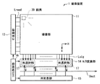
図1は、本開示の一実施の形態に係る撮像装置(撮像装置1)の全体のブロック構成を表すものである。撮像装置1は、撮像光に基づいて被写体の情報を読み取る(被写体を撮像する)ものである。この撮像装置1は、撮像部11、行走査部13、A/D変換部14、列走査部15およびシステム制御部16を備えている。これらのうち、行走査部13、A/D変換部14、列走査部15およびシステム制御部16が、本開示における「駆動部」の一具体例に対応する。
<Embodiment>
[Overall Configuration of Imaging Device 1]
FIG. 1 illustrates an overall block configuration of an imaging apparatus (imaging apparatus 1) according to an embodiment of the present disclosure. The
(撮像部11)
撮像部11は、入射した撮像光に応じて電気信号を発生させるもの(撮像領域)である。この撮像部11では、入射した撮像光の光量に応じた電荷量の光電荷を発生して内部に蓄積する光電変換部(後述する光電変換素子21)を有する画素(撮像画素,単位画素)20が、行列状(マトリクス状)に2次元配置されている。なお、図1中に示したように、以下、撮像部11内における水平方向(行方向)を「H」方向とし、垂直方向(列方向)を「V」方向として説明する。
(Imaging unit 11)
The
図2は、この撮像部11の概略構成例を表したものである。撮像部11には、上記した複数の画素20が配置された光電変換層111が設けられている。この光電変換層111では、図中に示したように、入射した撮像光Linに基づく光電変換(撮像光Linから信号電荷への変換)がなされるようになっている。
FIG. 2 illustrates a schematic configuration example of the
図3は、画素20の回路構成例(いわゆるパッシブ型の回路構成例)を、A/D変換部14内の後述する列選択部17の回路構成例とともに表したものである。このパッシブ型の画素20には、1つの光電変換素子21と、1つのトランジスタ22とが設けられている。この画素20にはまた、H方向に沿って延在する読み出し制御線Lreadと、V方向に沿って延在する信号線Lsigとが接続されている。
FIG. 3 illustrates a circuit configuration example of the pixel 20 (a so-called passive circuit configuration example) together with a circuit configuration example of a
光電変換素子21は、例えばPIN(Positive Intrinsic Negative)型のフォトダイオードからなり、前述したように、入射光(撮像光Lin)の光量に応じた電荷量の信号電荷を発生させるようになっている。なお、この光電変換素子21のカソードは、蓄積ノードNに接続されている。
The
トランジスタ22は、読み出し制御線Lreadから供給される行走査信号に応じてオン状態となることにより、光電変換素子21により得られた信号電荷(入力電圧Vin)を信号線Lsigへ出力するトランジスタ(読み出し用トランジスタ)である。このトランジスタ22は、ここではNチャネル型(N型)の電界効果トランジスタ(FET;Field Effect Transistor)により構成されている。ただし、トランジスタ22がPチャネル型(P型)のFET等により構成されていてもよい。このトランジスタ22はまた、例えば、微結晶シリコン(Si)または多結晶シリコン(ポリシリコン)等のシリコン系半導体を用いて構成されている。あるいは、酸化インジウムガリウム亜鉛(InGaZnO)または酸化亜鉛(ZnO)等の酸化物半導体を用いて構成してもよい。微結晶シリコン、多結晶シリコンおよび酸化物半導体は、非晶質シリコン(アモルファスシリコン)と比べて移動度μが高いため、例えばトランジスタ22による信号電荷の高速読み出しが可能となる。
The
この画素20では、トランジスタ22のゲートが読み出し制御線Lreadに接続され、ソースが信号線Lsigに接続され、ドレインが、光電変換素子21のカソード(蓄積ノードN)に接続されている。また、光電変換素子21のアノードは、ここではグランド(接地)に接続されている。
In the
(行走査部13)
図1に示した行走査部13は、例えば図示しないシフトレジスタ回路やアドレスデコーダ、論理回路等を含んで構成されており、撮像部11内の複数の画素20に対して行単位(水平ライン単位)での駆動(線順次走査)を行う画素駆動部(行走査回路)である。具体的には、後述する線順次読み出し駆動や線順次リセット駆動等の線順次撮像駆動の際に、そのような線順次走査を行う。なお、この線順次走査は、読み出し制御線Lreadを介して前述した行走査信号を各画素20へ供給することによって行われるようになっている。
(Row scanning unit 13)
The
(A/D変換部14)
A/D変換部14は、図1に示したように、複数(ここでは4つ)の信号線Lsigごとに1つ設けられた複数の列選択部17を有しており、信号線Lsigを介して入力した信号電圧(信号電荷)に基づいてA/D変換(アナログ/デジタル変換)を行うものである。これにより、デジタル信号からなる出力データDout(撮像信号)が生成され、外部へ出力されるようになっている。
(A / D converter 14)
As shown in FIG. 1, the A / D conversion unit 14 includes a plurality of
各列選択部17は、例えば図3および図4に示したように、チャージアンプ172、容量素子(コンデンサ,フィードバック容量素子)C1、スイッチSW1、サンプルホールド(S/H)回路173、4つのスイッチSW2を含むマルチプレクサ回路(選択回路)174、およびA/Dコンバータ175を有している。これらのうち、チャージアンプ172、容量素子C1、スイッチSW1、S/H回路173およびスイッチSW2はそれぞれ、図4に示したように、信号線Lsigごとに1つずつ設けられている。一方、マルチプレクサ回路174およびA/Dコンバータ175は、列選択部17全体として1つ設けられている。
Each
チャージアンプ172は、信号線Lsigから読み出された信号電荷を電圧に変換(Q−V変換)するためのアンプ(増幅器)である。このチャージアンプ172では、負側(−側)の入力端子に信号線Lsigの一端が接続され、正側(+側)の入力端子には所定のリセット電圧Vrstが入力されるようになっている。また、チャージアンプ172の出力端子と負側の入力端子との間は、容量素子C1とスイッチSW1との並列接続回路を介して帰還接続(フィードバック接続)されている。すなわち、容量素子C1の一方の端子がチャージアンプ172の負側の入力端子に接続され、他方の端子がチャージアンプ172の出力端子に接続されている。同様に、スイッチSW1の一方の端子がチャージアンプ172の負側の入力端子に接続され、他方の端子がチャージアンプ172の出力端子に接続されている。なお、このスイッチSW1のオン・オフ状態は、システム制御部16からアンプリセット制御線Lcarstを介して供給される制御信号(アンプリセット制御信号)によって制御されるようになっている。このようにして、チャージアンプ172、容量素子C1およびスイッチSW1によって、上記したQ−V変換を行うチャージアンプ回路が形成されている。
The
S/H回路173は、チャージアンプ172とマルチプレクサ回路174(スイッチSW2)との間に配置されており、チャージアンプ172からの出力電圧Vcaを一時的に保持するための回路である。
The S /
マルチプレクサ回路174は、列走査部15による走査駆動に従って4つのスイッチSW2のうちの1つが順次オン状態となることにより、各S/H回路173とA/Dコンバータ175との間を選択的に接続または遮断する回路である。これにより、チャージアンプ172(チャージアンプ回路)を用いて読み出された信号の一部を選択することが可能となっている。
The
A/Dコンバータ175は、スイッチSW2を介して入力されたS/H回路173からの出力電圧(マルチプレクサ回路174により選択された信号)に対してA/D変換を行うことにより、上記した出力データDoutを生成して出力する回路である。
The A /
(列走査部15・システム制御部16)
列走査部15は、例えば図示しないシフトレジスタやアドレスデコーダ等を含んで構成されており、上記した列選択部17内の各スイッチSW2を走査しつつ順番に駆動するものである。このような列走査部15による選択走査によって、信号線Lsigの各々を介して読み出された各画素20の信号(上記した出力データDout)が、順番に外部へ出力されるようになっている。
(
The
システム制御部16は、行走査部13、A/D変換部14および列走査部15の動作を制御するものである。具体的には、このシステム制御部16は、前述した各種のタイミング信号(制御信号)を生成するタイミングジェネレータを有しており、このタイミングジェネレータにおいて生成される各種のタイミング信号を基に、行走査部13、A/D変換部14および列走査部15の駆動制御を行う。このようにして、システム制御部16の制御に基づいて、行走査部13、A/D変換部14および列走査部15がそれぞれ撮像部11内の複数の画素20に対する撮像駆動(線順次撮像駆動)を行うことにより、撮像部11から出力データDoutが取得されるようになっている。
The
[撮像装置1の作用・効果]
(1.基本動作)
この撮像装置1では、図2に示したように、後述する露光期間Texにおいて撮像光Linが撮像部11へ入射すると、光電変換層111(図3に示した各画素20内の光電変換素子21)では、この撮像光Linが信号電荷に変換(光電変換)される。この光電変換によって発生した信号電荷により、蓄積ノードNでは蓄積ノード容量に応じた電圧変化が生じる。具体的には、蓄積ノード容量をCs、発生した信号電荷をqとすると、蓄積ノードNでは(q/Cs)の分だけ電圧が低下する。このような電圧変化に応じて、トランジスタ22のドレインには入力電圧Vin(信号電荷に対応した電圧)が印加される。このトランジスタ22へ供給される入力電圧Vinは、読み出し制御線Lreadから供給される行走査信号に応じてトランジスタ22がオン状態になると、その電荷が画素20から信号線Lsigへ読み出される(読み出し期間)。
[Operation and Effect of Imaging Device 1]
(1. Basic operation)
In the
このようにして読み出された信号電荷は、信号線Lsigを介して複数(ここでは4つ)の画素列ごとに、A/D変換部14内の列選択部17へ入力される。列選択部17では、まず、各信号線Lsigから入力される信号電荷ごとに、チャージアンプ172等からなるチャージアンプ回路においてQ−V変換(信号電荷から信号電圧への変換)を行う。次いで、変換された信号電圧(チャージアンプ回路からの出力電圧Vca)ごとに、S/H回路173およびマルチプレクサ回路174を介してA/Dコンバータ175においてA/D変換を行い、デジタル信号からなる出力データDout(撮像信号)を生成する。このようにして、各列選択部17から出力データDoutが順番に出力され、外部へ伝送される。
The signal charges read out in this way are input to the
(2.露光期間Tex・読み出し期間における動作)
ここで、図5(A),(B)を参照して、上記した露光期間Texおよび読み出し期間における画素20および列選択部17内のチャージアンプ回路の動作について、詳細に説明する。なお、以下では説明の便宜上、トランジスタ22のオン・オフ状態を、スイッチを用いて図示している。
(2. Operation during exposure period Tex and readout period)
Here, with reference to FIGS. 5A and 5B, operations of the
まず、図5(A)に示したように、画素20内の光電変換素子21へ撮像光Linが入射する露光期間Texでは、蓄積ノードNに蓄積された信号電荷が露光期間Tex中には信号線Lsig側へ出力されない(読み出されない)よう、トランジスタ22はオフ状態となっている。なお、このときチャージアンプ回路では、後述するアンプリセット動作(チャージアンプ回路のリセット動作)がなされた後の状態であるため、スイッチSW1がオン状態となっており、結果としてボルテージフォロワ回路が形成されている。
First, as shown in FIG. 5A, in the exposure period Tex in which the imaging light Lin is incident on the
一方、上記した読み出し期間は、本実施の形態では、画素20内に蓄積された電荷(信号電荷)をリセットするためのリセット動作(画素リセット動作)を行う期間ともなっている。すなわち、本実施の形態の画素20はパッシブ型の画素回路となっていることに起因して、光電変換素子21により得られた電荷を画素20から信号として読み出す「読み出し動作」と、上記した「画素リセット動作」とが、実質的に同時に(並行して)行われる。換言すると、詳細は後述するが、この読み出し動作を線順次で行うための線順次読み出し駆動と、画素リセット動作を線順次で行うための線順次リセット駆動とが、単一の線順次駆動によって(実質的に)同時に行われるようになっている。なお、このときの画素リセット動作は、後述する複数回(ここでは2回)の画素リセット動作のうちの1回目の画素リセット動作に対応していることから、以下では、この読み出し動作と1回目の画素リセット動作とが実質的同時に行われる期間を、「読み出し/第1リセット期間Tr1」と称する。
On the other hand, the above readout period is also a period for performing a reset operation (pixel reset operation) for resetting charges (signal charges) accumulated in the
この読み出し/第1リセット期間Tr1では、図5(B)に示したように、トランジスタ22がオン状態となることにより、画素20内の蓄積ノードNから信号線Lsig側へ信号電荷が読み出される(図中の矢印P11参照)。このようにして読み出された信号電荷は、チャージアンプ回路へ入力される。ここで、この読み出し/第1リセット期間Tr1では、チャージアンプ回路におけるスイッチSW1は、オフ状態となっている。すなわち、チャージアンプ回路が読み出し動作状態となっている。したがって、このチャージアンプ回路へ入力された信号電荷は容量素子C1に蓄積され、その蓄積電荷に応じた信号電圧(出力電圧Vca)がチャージアンプ172から出力される。このようにしてチャージアンプ回路において、信号電荷から信号電圧への変換(Q−V変換)がなされる。なお、このようにして容量素子C1に蓄積された電荷は、後述するアンプリセット動作の際にスイッチSW1がオン状態となることにより、リセットされる(アンプリセット動作がなされる)ようになっている。
In the readout / first reset period Tr1, as shown in FIG. 5B, the
また、このような読み出し動作とともに、この読み出し/第1リセット期間Tr1では、以下のようにして1回目の画素リセット動作(第1の画素リセット動作)が行われる。すなわち、図中の矢印P12で示したように、チャージアンプ回路(チャージアンプ172)における仮想短絡(イマジナリー・ショート)現象を利用して、1回目の画素リセット動作がなされる。つまり、この仮想短絡現象によって、チャージアンプ172における負側の入力端子側(信号線Lsig側)の電圧が、正側の入力端子に印加されているリセット電圧Vrstに略等しくなることから、トランジスタ22を介して画素20内の蓄積ノードNも、このリセット電圧Vrstとなるのである。このようにして、上記した読み出し動作に伴い、蓄積ノードNの蓄積電荷が所定のリセット電圧Vrstにリセットされる。
In addition to the readout operation, the first pixel reset operation (first pixel reset operation) is performed in the readout / first reset period Tr1 as follows. That is, as indicated by an arrow P12 in the figure, the first pixel reset operation is performed using the virtual short circuit (imaginary short) phenomenon in the charge amplifier circuit (charge amplifier 172). That is, due to this virtual short-circuit phenomenon, the voltage on the negative input terminal side (signal line Lsig side) of the
(3.複数回の画素リセット動作を利用した残留電荷の低減作用)
ところで、上記のような1回目の画素リセット動作を行ったにも関わらず、この1回目の画素リセット動作前に蓄積された信号電荷の一部が、画素20内に残存してしまう場合がある。このように信号電荷の一部が画素20内に残ってしまうと、次の読み出し動作時(次のフレーム期間での撮像時)においてその残留電荷に起因した残像が発生し、撮像画質が低下してしまうという問題がある。
(3. Reducing residual charge using multiple pixel reset operations)
By the way, in spite of performing the first pixel reset operation as described above, a part of the signal charge accumulated before the first pixel reset operation may remain in the
そこで本実施の形態では、例えば図6および図7に示したように、複数回(ここでは2回)の画素リセット動作を行うことによって上記した残留電荷を低減し、この残留電荷に起因した残像を抑えるようにしている。以下、この複数回の画素リセット動作を利用した残留電荷の低減作用について、詳細に説明する。 Therefore, in the present embodiment, for example, as shown in FIGS. 6 and 7, the residual charge is reduced by performing the pixel reset operation a plurality of times (here, twice), and the afterimage caused by the residual charge is reduced. I try to suppress it. Hereinafter, the residual charge reducing action using the plurality of pixel reset operations will be described in detail.
図6において、(A)は読み出し制御線Lreadの電位Vreadのタイミング波形を、(B)は、チャージアンプ172からの出力電圧Vcaのタイミング波形を、(C)は信号線Lsigの電位Vsigのタイミング波形を、(D)は蓄積ノードNの電位Vnのタイミング波形を、それぞれ示す。また、これらの各タイミング波形は、1垂直期間(1フレーム期間)ΔTvを含む前後の期間についてのものである。
6A is a timing waveform of the potential Vread of the read control line Lread, FIG. 6B is a timing waveform of the output voltage Vca from the
また、図7は、本実施の形態に係る線順次撮像駆動(線順次読み出し駆動および線順次リセット駆動)の一例を、タイミング波形図で表わしたものである。ここで、(A)〜(F)はそれぞれ、n本の読み出し制御線Lread(1)〜Lread(3),Lread(n−2)〜Lread(n)の電位Vread(1)〜Vread(3),Vread(n−2)〜Vread(n)のタイミング波形を示している。また、図中に示したΔThは、1水平期間(1水平走査期間)を表している。更に、ΔTr1は、1回目の画素リセット動作等(第1読み出し/リセット期間Tr1の動作)についての線順次駆動期間を、ΔTr2は、2回目の画素リセット動作等(第1読み出し/リセット期間Tr1の動作)についての線順次駆動期間を、それぞれ表している。 FIG. 7 is a timing waveform diagram showing an example of line-sequential imaging driving (line-sequential readout driving and line-sequential reset driving) according to the present embodiment. Here, (A) to (F) are potentials Vread (1) to Vread (3) of n read control lines Lread (1) to Lread (3) and Lread (n−2) to Lread (n), respectively. ), Vread (n-2) to Vread (n). Further, ΔTh shown in the drawing represents one horizontal period (one horizontal scanning period). Further, ΔTr1 is a line sequential drive period for the first pixel reset operation or the like (operation in the first readout / reset period Tr1), and ΔTr2 is a second pixel reset operation or the like (in the first readout / reset period Tr1). Line-sequential driving periods for (operation) are respectively shown.
この1フレーム期間ΔTvでは、まずタイミングt11〜t12の露光期間Texにおいて、図5(A)等を用いて前述したようにして、露光動作が行われる。すなわち、撮像光Linが撮像部11へ入射すると、各画素20内の光電変換素子21では、この撮像光Linが信号電荷に変換(光電変換)される。そして、この信号電荷が画素20内の蓄積ノードNに蓄積され、その電位Vnが徐々に変化する(図6中の矢印P31参照)。なお、この露光動作に伴って、電位Vnがリセット電圧Vrst側から0Vへ向けて徐々に低下していっているのは、ここでは光電変換素子21のカソード側が蓄積ノードNに接続されているためである。
In this one frame period ΔTv, first, an exposure operation is performed in the exposure period Tex at timings t11 to t12 as described above with reference to FIG. That is, when the imaging light Lin enters the
次いで、タイミングt13〜t14の読み出し/第1リセット期間Tr1では、図5(B)等を用いて前述したようにして、読み出し動作と1回目の画素リセット動作とが行われる。すなわち、画素20から信号電荷を読み出すことによってこの信号電荷に対応する撮像信号D11を取得する読み出し動作と、この画素20内の信号電荷をリセットするための1回目の画素リセット動作とが、実質的に同時に行われる。ただし、図6中の矢印P32で示したように、この1回目の画素リセット動作後において蓄積ノードNの電位Vnが徐々に低下していき、前述した残留電荷q1が発生してしまっている。
Next, in the readout / first reset period Tr1 at timings t13 to t14, the readout operation and the first pixel reset operation are performed as described above with reference to FIG. That is, the readout operation for acquiring the imaging signal D11 corresponding to the signal charge by reading out the signal charge from the
なお、例えばその後のタイミングt15では、チャージアンプ回路におけるスイッチSW1がオン状態となることにより、このチャージアンプ回路内の容量素子C1に蓄積された電荷がリセットされる。すなわち、チャージアンプ回路のリセット動作(アンプリセット動作)が行われる。 For example, at the subsequent timing t15, the switch SW1 in the charge amplifier circuit is turned on, whereby the charge accumulated in the capacitive element C1 in the charge amplifier circuit is reset. That is, the reset operation (amplifier reset operation) of the charge amplifier circuit is performed.
続いて、その後のタイミングt16〜t17において、以下説明する2回目の画素リセット動作(第2の画素リセット動作)が行われる(第2リセット期間Tr2)。 Subsequently, at subsequent timings t16 to t17, a second pixel reset operation (second pixel reset operation) described below is performed (second reset period Tr2).
この第2リセット期間Tr2では、具体的には、例えば図8(A)に示した第1の動作例のようにして、2回目の画素リセット動作が行われる。すなわち、この第1の動作例では、画素20内のトランジスタ22がオン状態になると共に、チャージアンプ回路におけるスイッチSW1もオン状態となり、チャージアンプ172を用いたボルテージフォロワ回路が形成される。このため、このチャージアンプ172における帰還特性(フィードバック特性)により、チャージアンプ172における負側の入力端子側(信号線Lsig側)の電圧が、正側の入力端子に印加されているリセット電圧Vrstに略等しくなる。このように第1の動作例では、チャージアンプ172における帰還特性を利用して、画素20内の蓄積ノードNの電位Vnがリセット電圧Vrstに設定される(2回目の画素リセット動作がなされる)。
Specifically, in the second reset period Tr2, for example, the second pixel reset operation is performed as in the first operation example illustrated in FIG. That is, in this first operation example, the
一方、図8(B)に示した第2の動作例では、前述した1回目の画素リセット動作のときと同様に、チャージアンプ回路(チャージアンプ172)における仮想短絡現象を利用して、2回目の画素リセット動作がなされる(図中の矢印P42参照)。つまり、この仮想短絡現象によって、画素20内の蓄積ノードNの電位Vnがリセット電圧Vrstに設定される。なお、このときは、読み出し/第1リセット期間Tr1のときと同様に、画素20内のトランジスタ22がオン状態であると共にチャージアンプ回路におけるスイッチSW1がオフ状態であることから、チャージアンプ回路が読み出し動作状態となっている。つまり、図中の矢印P41で示したように、この第2の動作例では、蓄積ノードNに残存している電荷をチャージアンプ回路によって読み出すことも可能となっている。
On the other hand, in the second operation example shown in FIG. 8B, as in the case of the first pixel reset operation described above, the virtual short-circuit phenomenon in the charge amplifier circuit (charge amplifier 172) is used for the second operation. The pixel reset operation is performed (see arrow P42 in the figure). That is, the potential Vn of the storage node N in the
このようにして本実施の形態では、画素20内の蓄積電荷の画素リセット動作(後述する線順次リセット駆動)が、1フレーム期間内で間欠的に(独立して)複数回行われる。具体的には、ここでは1回目の画素リセット動作(読み出し/第1リセット期間Tr1)と2回目の画素リセット動作(第2リセット期間Tr2)とが、間欠的に行われるように設定されている。これにより、1回目の画素リセット動作後における画素20内の残留電荷(信号電荷の残存量)がより確実にリセットされ、そのような残留電荷が低減される(図6中に示した矢印P33参照)。
In this manner, in the present embodiment, the pixel reset operation (line-sequential reset driving described later) of accumulated charges in the
なお、このような複数回の画素リセット動作(線順次リセット駆動)は、例えば1水平期間(1水平走査期間:一例として32μs程度)を超える期間に亘って間欠的に行われるようにするのが望ましい。これは、以下の理由によるものである。すなわち、例えばPIN型のフォトダイオードにおける状態遷移には、数百μs程度の時間がかかる。このことから、例えば100μs程度の時間、リセット電圧Vrstを連続的または間欠的に蓄積ノードNに与えることで、残留電荷の発生を低減することができると考えられる。ただし、実際には、このリセット電圧Vrstを与える期間が1水平期間(例えば32μs程度)を超えると残留電荷が大きく減少し始めることが、実験等により確認されている。 It should be noted that such a plurality of pixel reset operations (line-sequential reset driving) are performed intermittently over a period exceeding, for example, one horizontal period (one horizontal scanning period: about 32 μs as an example). desirable. This is due to the following reason. That is, for example, a state transition in a PIN type photodiode takes about several hundred μs. From this, it is considered that the generation of residual charges can be reduced by applying the reset voltage Vrst to the storage node N continuously or intermittently for a time of, for example, about 100 μs. However, in practice, it has been confirmed by experiments and the like that the residual charge starts to greatly decrease when the period during which the reset voltage Vrst is applied exceeds one horizontal period (for example, about 32 μs).
(4.各リセット動作のタイミング等について)
また、本実施の形態では、例えば以下の図9〜図16に示したようにして、線順次撮像駆動(線順次読み出し駆動および線順次リセット駆動)の際の、各リセット動作(画素リセット動作およびアンプリセット動作)のタイミングや期間が設定されている。
(4. Timing of each reset operation)
In this embodiment, for example, as shown in FIGS. 9 to 16 below, each reset operation (pixel reset operation and pixel sequential drive and line sequential read drive and line sequential reset drive) in line sequential imaging drive (line sequential read drive and line sequential reset drive) is performed. The timing and period of the unpreset operation are set.
すなわち、例えば図9(A),図9(B)または図9(C)に示したように、画素リセット動作を行う画素リセット期間Tprstの終了タイミングと、アンプリセット動作を行うアンプリセット期間Tarstの終了タイミングとのうちの一方が、所定の電源電位不安定化期間内に含まれないように設定されている(図中の矢印参照)。あるいは、例えば図10(A),図10(B)または図10(C)に示したように、画素リセット期間Tprstの終了タイミングとアンプリセット期間Tarstの終了タイミングとの双方が、所定の電源電位不安定化期間内に含まれないように設定されている(図中の矢印参照)。また、特に図9(A)および図10(A)に示したように、画素リセット期間Tprstの全期間(画素リセット動作の全期間)またはアンプリセット期間Tarstの全期間(アンプリセット動作の全期間)が、この電源電位不安定化期間内に含まれないようにするのが望ましい。 That is, for example, as illustrated in FIG. 9A, FIG. 9B, or FIG. 9C, the end timing of the pixel reset period Tprst in which the pixel reset operation is performed and the amplifier reset period Tarst in which the amplifier reset operation is performed. One of the end timings is set so as not to be included in a predetermined power supply potential instability period (see arrow in the figure). Alternatively, for example, as shown in FIG. 10A, FIG. 10B, or FIG. 10C, both the end timing of the pixel reset period Tprst and the end timing of the amplifier reset period Tarst have a predetermined power supply potential. It is set not to be included in the instability period (see arrow in the figure). In particular, as shown in FIGS. 9A and 10A, the entire period of the pixel reset period Tprst (the entire period of the pixel reset operation) or the entire period of the amplifier reset period Tarst (the entire period of the amplifier reset operation) ) Is not included in the power supply potential instability period.
ここで、画素リセット期間Tprstとは、ここでは読み出し/第1リセット期間Tr1および第2リセット期間Tr2の双方の期間を意味している。また、ここでいう「電源電位不安定化期間」とは、グランド電位(接地電位)を含む電源電位が揺れてしまっている(不安定になっている)期間のことである。具体的には、例えば図9中に示したように、マルチプレクサ動作期間Tmux(マルチプレクサ回路174の動作期間)や、A/D変換期間Tadc(A/Dコンバータ175の動作期間)など(これら2つの動作期間のうちの少なくとも一方)を含んでいる。 Here, the pixel reset period Tprst here means both the readout / first reset period Tr1 and the second reset period Tr2. In addition, the “power supply potential instability period” referred to here is a period in which the power supply potential including the ground potential (ground potential) fluctuates (becomes unstable). Specifically, for example, as shown in FIG. 9, the multiplexer operation period Tmux (the operation period of the multiplexer circuit 174), the A / D conversion period Tadc (the operation period of the A / D converter 175), etc. At least one of the operation periods).
ここで、これらの画素リセット期間Tprstやアンプリセット期間Tarstの終了タイミングを、上記した電源電位不安定化期間から避けて(外して)設定しているのは、リセット電圧Vrst等の不安定化に起因した撮像信号(出力データDout)におけるノイズ成分を低減するためである。以下、このノイズ成分に関する問題について詳述する。 Here, the end timing of the pixel reset period Tprst and the amplifier reset period Tarst is set so as to be avoided (excluded) from the power supply potential instability period in order to destabilize the reset voltage Vrst and the like. This is to reduce the noise component in the resulting imaging signal (output data Dout). Hereinafter, the problem relating to the noise component will be described in detail.
まず、例えば図4に示したように、マルチプレクサ回路174内には多数のスイッチSW2が設けられていることから、これらのスイッチSW2のオン・オフ状態を切り換える際に、電源(接地電源等)にノイズ(スイッチング・ノイズ)が乗り易い。また、一般にデジタル信号を扱う回路は、ノイズ源となり易い。これは、デジタル信号は、2つの電圧レベル(ハイ・レベルおよびロー・レベル)を急峻に切り替えることによって得られることから、これらの電圧レベル間での切り換え時に、高周波成分のノイズが発生するためである。このような高周波成分のノイズは主にデジタル系の電源(接地電源等)に乗っていき、アナログ系の電源と分離するように設計されていても、多少影響してしまう。そして、一般にA/Dコンバータでは、アナログ系とデジタル系とが直近に存在するため、特に影響が大きくなる。
First, for example, as shown in FIG. 4, since a large number of switches SW2 are provided in the
このように、マルチプレクサ動作期間TmuxやA/D変換期間Tadcでは電源が揺れてしまう(電源電位が不安定となってしまう)ことから、これらの期間内に画素リセット期間Tprstやアンプリセット期間Tarstの終了タイミングが含まれると、以下のようなノイズの問題が生じる。 Thus, since the power supply fluctuates (the power supply potential becomes unstable) during the multiplexer operation period Tmux and the A / D conversion period Tadc, the pixel reset period Tprst and the amplifier reset period Tarst are included in these periods. When the end timing is included, the following noise problem occurs.
すなわち、まず、電源電位が不安定となっていることに起因してリセット電圧Vrstも揺れていると、前述したチャージアンプ回路における仮想短絡(イマジナリー・ショート)現象により、信号線Lsigの電位Vsigも揺れてしまう。このような状態で画素リセット動作(画素リセット期間Tprst)がなされると、揺れているリセット電圧Vrstで画素20内の電荷がリセットされる。そして、このようにリセット電圧Vrstが揺れている状態で画素リセット期間Tprstが終了となると、不安定な電圧状態で画素20内のトランジスタ22がオフ状態となるため、蓄積ノードNの電位(および接地電位)が画素リセット動作の度にばらついてしまう。つまり、光電変換素子21のアノード側およびカソード側の電位がそれぞればらついてしまい、それが撮像信号におけるノイズ成分として現れ、S/N比の低下につながるのである。
That is, first, when the reset voltage Vrst fluctuates due to the unstable power supply potential, the potential Vsig of the signal line Lsig is also caused by the virtual short circuit (imaginary short) phenomenon in the charge amplifier circuit described above. It will shake. When the pixel reset operation (pixel reset period Tprst) is performed in such a state, the charges in the
また、アンプリセット動作(アンプリセット期間Tarst)の際には、前述した理由により、チャージアンプ172における正側および負側の入力端子における電圧は、互いに等しくなっている。ところが、このアンプリセット期間Tarstが終了してからリセット電圧Vrstが揺れると、正側および負側の入力端子に電位差が生じ、チャージアンプ172の出力電圧Vcaが変化する。このようにしてチャージアンプ172の出力電圧Vcaが変化すると、フィードバックがかかるため、容量素子C1と信号線Lsigの容量との容量比に応じて負側の入力端子の電圧が変化する。その結果、画素20から撮像信号を読み出していない状態でも容量素子C1に電荷が蓄積されてしまい(容量素子C1の両端間に電圧が発生し)、それがそのまま撮像信号におけるノイズ成分として現れてしまう。
In the amplifier reset operation (amplifier reset period Tarst), the voltages at the positive and negative input terminals of the
これらの理由により本実施の形態では、上記した図9および図10のように、画素リセット期間Tprstの終了タイミングおよびアンプリセット期間Tarstの終了タイミングのうちの少なくとも一方が、上記した電源電位不安定化期間内に含まれないように、各画素20の駆動が行われる。これにより、例えば図11(A),(B)に示した比較例のように、画素リセット期間Tprstやアンプリセット期間Tarstの終了タイミングが電源電位不安定化期間内に含まれる場合と比べ、上記したリセット電圧Vrstの不安定化に起因した撮像信号におけるノイズ成分が低減する。
For these reasons, in the present embodiment, as shown in FIGS. 9 and 10, at least one of the end timing of the pixel reset period Tprst and the end timing of the amplifier reset period Tarst is the power supply potential instability described above. Each
また、本実施の形態では、例えば図12(A)に示したように、画素リセット期間Tprstとアンプリセット期間Tarstとが互いにオーバーラップ(重畳)していない場合よりも、例えば図12(B)〜(D)に示したように、これらの期間の少なくとも一部が互いにオーバーラップしているほうが望ましい。具体的には、図12(B)に示した例では、画素リセット期間Tprstとアンプリセット期間Tarstとの一部が互いにオーバーラップしており、オーバーラップ期間ΔTolとなっている。また、図12(C)に示した例では、画素リセット期間Tprstおよびアンプリセット期間Tarstの全期間が互いにオーバーラップしており、オーバーラップ期間ΔTolとなっている。つまり、これらの画素リセット期間Tprstとアンプリセット期間Tarstとが、互いに一致している。更に、図12(D)に示した例では、アンプリセット期間Tarst内に画素リセット期間Tprst全体(開始タイミングから終了タイミングまでの全期間)が含まれるようにして、オーバーラップ期間ΔTolが設けられている。このように、画素リセット期間Tprstとアンプリセット期間Tarstとの少なくとも一部が互いにオーバーラップしているようにした場合、リセット動作時間の短縮化を図ることができ、フレームレートの低下を最低限に抑えつつ(あるいは低下することなく)、上記したノイズ成分を低減してS/N比を向上させることが可能となる。 Further, in the present embodiment, for example, as shown in FIG. 12A, for example, as shown in FIG. 12B, the pixel reset period Tprst and the amplifier reset period Tarst are not overlapped with each other. As shown in (D), it is desirable that at least a part of these periods overlap each other. Specifically, in the example shown in FIG. 12B, part of the pixel reset period Tprst and the amplifier reset period Tarst overlap each other, which is the overlap period ΔTol. In the example shown in FIG. 12C, the entire pixel reset period Tprst and amplifier reset period Tarst overlap each other, which is an overlap period ΔTol. That is, the pixel reset period Tprst and the amplifier reset period Tarst coincide with each other. Furthermore, in the example shown in FIG. 12D, an overlap period ΔTol is provided so that the entire pixel reset period Tprst (all periods from the start timing to the end timing) is included in the amplifier reset period Tarst. Yes. As described above, when at least a part of the pixel reset period Tprst and the amplifier reset period Tarst are overlapped with each other, the reset operation time can be shortened and the decrease in the frame rate is minimized. While suppressing (or not decreasing), it is possible to improve the S / N ratio by reducing the noise component described above.
ここで、前述した図7中の符号P5で示した期間付近のタイミング波形を拡大して示すと、各リセット動作(画素リセット動作およびアンプリセット動作)のタイミングや期間は、詳細には例えば図13〜図16に示したようになる。なお、これらの図13〜図16ではそれぞれ、前述したアンプリセット制御線Lcarstの電位Vcarstを、前述した第1の動作例の場合(各図の(D))および第2の動作例の場合(各図の(E))の各々について示している。 Here, when the timing waveform in the vicinity of the period indicated by the symbol P5 in FIG. 7 is enlarged, the timing and period of each reset operation (pixel reset operation and amplifier reset operation) are shown in detail in FIG. As shown in FIG. 13 to 16, the potential Vcarst of the amplifier reset control line Lcarst described above is set in the case of the above-described first operation example ((D) in each drawing) and the case of the second operation example ( It shows about each of (E)) of each figure.
まず、図13および図14に示した例では、符号P5または符号P5aで示した期間内において、以下のように設定されている。すなわち、Vread(2)(第2リセット期間Tr2)→Vread(n−2)(読み出し/第1リセット期間Tr1)→Vread(3)(第2リセット期間Tr2)の順に、行走査信号に相当する電位Vreadが印加されている。また、特に図14に示した例では、アンプリセット期間Tarstの一部(開始タイミングから途中までの期間)が、電源電位不安定化期間(マルチプレクサ動作期間TmuxやA/D変換期間Tadc等)の一部とオーバーラップしている。そして、これらの例ではそれぞれ、図中の矢印で示したように、画素リセット期間Tprstの終了タイミングおよびアンプリセット期間Tarstの終了タイミングがそれぞれ、この電源電位不安定化期間内に含まれないように設定されている。 First, in the example shown in FIG. 13 and FIG. 14, the following settings are made within the period indicated by the symbol P5 or the symbol P5a. That is, it corresponds to the row scanning signal in the order of Vread (2) (second reset period Tr2) → Vread (n−2) (reading / first reset period Tr1) → Vread (3) (second reset period Tr2). A potential Vread is applied. In particular, in the example shown in FIG. 14, a part of the amplifier reset period Tarst (period from the start timing to the middle) is a power supply potential instability period (multiplexer operation period Tmux, A / D conversion period Tadc, etc.). It overlaps with a part. In each of these examples, as indicated by arrows in the drawing, the end timing of the pixel reset period Tprst and the end timing of the amplifier reset period Tarst are not included in the power supply potential instability period, respectively. Is set.
一方、図15および図16に示した例では、符号P5bまたは符号P5cで示した期間内において、図13,図14中に示した符号P5,P5aの期間とは異なり、以下の順番で、行走査信号に相当する電位Vreadが印加されている。すなわち、Vread(n−2)(読み出し/第1リセット期間Tr1)→Vread(2)(第2リセット期間Tr2)→Vread(3)(第2リセット期間Tr2)の順に、電位Vreadが印加されている。また、特に図16に示した例では、アンプリセット期間Tarstの一部(途中の期間)が、電源電位不安定化期間(マルチプレクサ動作期間TmuxやA/D変換期間Tadc等)とオーバーラップしている。そして、これらの例ではそれぞれ、図中の矢印で示したように、画素リセット期間Tprstの終了タイミングおよびアンプリセット期間Tarstの終了タイミングがそれぞれ、この電源電位不安定化期間内に含まれないように設定されている。 On the other hand, in the example shown in FIG. 15 and FIG. 16, in the period indicated by the symbol P5b or the symbol P5c, unlike the periods indicated by the symbols P5 and P5a shown in FIG. A potential Vread corresponding to the scanning signal is applied. That is, the potential Vread is applied in the order of Vread (n−2) (reading / first reset period Tr1) → Vread (2) (second reset period Tr2) → Vread (3) (second reset period Tr2). Yes. In particular, in the example shown in FIG. 16, a part of the amplifier reset period Tarst (intermediate period) overlaps with the power supply potential instability period (multiplexer operation period Tmux, A / D conversion period Tadc, etc.). Yes. In each of these examples, as indicated by arrows in the drawing, the end timing of the pixel reset period Tprst and the end timing of the amplifier reset period Tarst are not included in the power supply potential instability period, respectively. Is set.
以上のように本実施の形態では、読出し動作、画素リセット動作およびアンプリセット動作がそれぞれ行われるように各画素20を駆動すると共に、画素リセット動作(画素リセット期間Tprst)の終了タイミングおよびアンプリセット動作(アンプリセット期間Tarst)の終了タイミングのうちの少なくとも一方が、所定の電源電位不安定化期間内に含まれないように、各画素20の駆動を行う。これにより、撮像信号におけるノイズ成分を低減する(S/N比を向上させる)ことができ、撮像画像の高画質化を実現することが可能となる。
As described above, in the present embodiment, each
特に、画素リセット期間Tprstの終了タイミングが電源電位不安定化期間内に含まれないようにした場合には、アンプリセット期間Tarstの終了タイミングが電源電位不安定化期間内に含まれないようにした場合と比べ、以下の理由により、更にS/N比を向上させて更なる撮像画像の高画質化を図ることが可能となる。すなわち、画素20から電荷を読み出す際にゲインがかかるため、画素20におけるリセット電圧Vrstの揺れが大きくなり、出力に現れてしまう(ノイズもゲイン倍されてしまう)ためである。ただし、このゲインの値が小さい場合などには、タイミングの設定等により、逆になる場合もあり得る。なお、上記したゲインは、画素容量Cpdと容量素子C1との容量比により規定されるものであり(ゲインG=(Cpd/C1))、G≧1の場合が多いが、G<1の場合もあり得る。
In particular, when the end timing of the pixel reset period Tprst is not included in the power supply potential instability period, the end timing of the amplifier reset period Tarst is not included in the power supply potential instability period. Compared to the case, it is possible to further improve the image quality of the captured image by further improving the S / N ratio for the following reason. That is, since a gain is applied when reading out electric charges from the
<変形例>
続いて、上記実施の形態の変形例(変形例1〜8)について説明する。なお、実施の形態における構成要素と同一のものには同一の符号を付し、適宜説明を省略する。
<Modification>
Subsequently, modified examples (modified examples 1 to 8) of the above-described embodiment will be described. In addition, the same code | symbol is attached | subjected to the same component as embodiment, and description is abbreviate | omitted suitably.
[変形例1]
図17は、変形例1に係る画素(画素20A)の回路構成を、上記実施の形態で説明した列選択部17の回路構成例とともに表したものである。本変形例の画素20Aは、実施の形態の画素20と同様にいわゆるパッシブ型の回路構成となっており、1つの光電変換素子21と1つのトランジスタ22とを有している。また、この画素20Aには画素20と同様に、H方向に沿って延在する読み出し制御線Lreadと、V方向に沿って延在する信号線Lsigとが接続されている。
[Modification 1]
FIG. 17 illustrates the circuit configuration of the pixel (pixel 20A) according to the first modification example together with the circuit configuration example of the
ただし、画素20Aでは、光電変換素子21の配置方向(向き)が、画素20とは逆になっている。すなわち、この画素20Aでは、光電変換素子21のアノードが蓄積ノードNに接続され、カソードがグランド(接地)に接続されている。ただし、この光電変換素子21のカソードが、グランド以外の他の電源電位に接続されているようにしてもよい。
However, in the
このような構成の画素20Aを有する撮像装置においても、上記実施の形態の撮像装置1と同様の作用により同様の効果を得ることが可能である。
Even in the imaging apparatus having the pixel 20A having such a configuration, the same effect can be obtained by the same operation as that of the
[変形例2,3]
(回路構成)
図18は、変形例2に係る画素(画素20B)の回路構成を、以下説明する列選択部17Bの回路構成例とともに表したものである。また、図19は、変形例3に係る画素(画素20C)の回路構成を、列選択部17Bの回路構成例とともに表したものである。これらの変形例2,3に係る画素20B,20Cはそれぞれ、これまで説明した画素20,20Aとは異なり、いわゆるアクティブ型の回路構成となっている。
[
(Circuit configuration)
FIG. 18 illustrates a circuit configuration of a pixel (pixel 20B) according to
具体的には、このアクティブ型の画素20B,20Cには、1つの光電変換素子21と、3つのトランジスタ22,23,24とが設けられている。これらの画素20B,20Cにはまた、H方向に沿って延在する読み出し制御線Lreadおよびリセット制御線Lrstと、V方向に沿って延在する信号線Lsigとが接続されている。
Specifically, the active pixels 20B and 20C are provided with one
画素20B,20Cではそれぞれ、トランジスタ22のゲートが読み出し制御線Lreadに接続され、ソースが信号線Lsigに接続され、ドレインが、ソースフォロワ回路を構成するトランジスタ23のドレインに接続されている。トランジスタ23のソースは電源VDDに接続され、ゲートは、光電変換素子21のカソード(図18に示した画素20B)またはアノード(図19に示した画素20C)(蓄積ノードN)と、リセット用トランジスタとして機能するトランジスタ24のドレインとに接続されている。このトランジスタ24のゲートはリセット制御線Lrstに接続され、ソースにはリセット電圧Vrstが印加されるようになっている。光電変換素子21のアノード(画素20B)またはカソード(画素20C)は、グランド(接地)に接続されている。ただし、画素20Cの場合、光電変換素子21のカソードが、グランド以外の他の電源電位に接続されているようにしてもよい。
In each of the pixels 20B and 20C, the gate of the
また、図18および図19に示した変形例2,3に係る列選択部17Bは、前述した列選択部17において、チャージアンプ172、容量素子C1およびスイッチSW1の代わりに、定電流源171およびアンプ176を設けたものとなっている。アンプ176では、正側の入力端子には信号線Lsigが接続されると共に、負側の入力端子と出力端子とが互いに接続され、ボルテージフォロワ回路が形成されている。なお、信号線Lsigの一端側には定電流源171の一方の端子が接続され、この定電流源171の他方の端子には電源VSSが接続されている。
In addition, the
(作用・効果)
このようなアクティブ型の回路構成からなる画素20B,20Cを有する変形例2,3の撮像装置では、以下のようにして撮像動作(線順次撮像駆動)がなされる。
(Action / Effect)
In the imaging devices of
すなわち、まず、これまで説明したパッシブ型の回路構成からなる画素20,20Aを有する撮像装置では、例えば図20(A)に示したようにして線順次撮像駆動が行われる。具体的には、線順次読み出し駆動と線順次リセット駆動とが、単一の線順次駆動(読み出し/第1リセット期間Tr1の線順次動作を行うための駆動)によって、実質的に同時に行われる。
That is, first, in the imaging apparatus having the
これに対して、変形例2,3のように、アクティブ型の回路構成からなる画素20B,20Cを有する撮像装置では、例えば図20(B)に示したようにして線順次撮像駆動が行われる。具体的には、線順次読み出し駆動と各回(ここでは1回目および2回目)の線順次リセット駆動とが、互いに独立して個別に行われる。すなわち、読み出し期間Tr1aの線順次動作を行うための線順次読み出し駆動と、1回目の画素リセット期間(第1リセット期間Tr1b)の線順次動作を行うための1回目の線順次リセット駆動と、2回目の画素リセット期間(第2リセット期間Tr2)の線順次動作を行うための2回目の線順次リセット駆動とが、互いに独立して個別に行われる。なお、このアクティブ型の回路構成の場合、各回の線順次リセット駆動の際の画素リセット動作は、リセット用トランジスタとして機能するトランジスタ24がオン状態となることによって行われる。
On the other hand, in the imaging apparatus having the pixels 20B and 20C having the active circuit configuration as in the second and third modifications, line-sequential imaging driving is performed as shown in FIG. 20B, for example. . Specifically, line-sequential readout driving and line-sequential reset driving each time (here, the first and second times) are performed independently of each other. That is, a line-sequential readout drive for performing a line-sequential operation in the readout period Tr1a, a first line-sequential reset drive for performing a line-sequential operation in the first pixel reset period (first reset period Tr1b), and 2 The second line sequential reset driving for performing the line sequential operation in the second pixel reset period (second reset period Tr2) is performed independently of each other. Note that in the case of this active circuit configuration, the pixel reset operation in each line-sequential reset drive is performed when the
このように、アクティブ型の回路構成からなる画素20B,20Cを有する撮像装置においても、これまで説明したパッシブ型の回路構成の場合と同様の効果が得られる。すなわち、画素リセット動作の終了タイミングおよびアンプリセット動作の終了タイミングのうちの少なくとも一方が電源電位不安定化期間内に含まれないように、各画素20の駆動を行うことにより、S/N比を向上させることができ、撮像画像の高画質化を実現することが可能となる。
As described above, even in the imaging apparatus having the pixels 20B and 20C having the active circuit configuration, the same effects as those of the passive circuit configuration described so far can be obtained . That is, by driving each
[変形例4]
図21(A)〜(C)および図22(A)〜(C)はそれぞれ、変形例4に係る撮像駆動例をタイミング図で表わしたものである。
[Modification 4]
FIGS. 21A to 21C and FIGS. 22A to 22C are timing diagrams illustrating an imaging driving example according to the fourth modification.
まず、図21(A),(B)に示した例では、上記した読み出し期間Tr1aの線順次動作を行うための線順次読み出し駆動と、画素リセット期間(リセット期間Tr1b)の線順次動作を行うための線順次リセット駆動とが、互いに独立して個別に行われている。具体的には、図21(A)の例では、これらの線順次読み出し駆動と線順次リセット駆動との間でオーバーラップ期間が設けられていない一方、図21(B)の例では、線順次読み出し駆動と線順次リセット駆動との間でオーバーラップ期間が設けられている。 First, in the example shown in FIGS. 21A and 21B, the line-sequential readout drive for performing the line-sequential operation in the readout period Tr1a and the line-sequential operation in the pixel reset period (reset period Tr1b) are performed. The line-sequential reset driving is performed independently of each other. Specifically, in the example of FIG. 21A, no overlap period is provided between the line-sequential readout drive and the line-sequential reset drive, whereas in the example of FIG. An overlap period is provided between the read drive and the line sequential reset drive.
また、図21(C)に示した例では、読み出し/リセット期間Tr1の線順次動作を行うための線順次駆動のみが行われている。 In the example shown in FIG. 21C, only the line sequential drive for performing the line sequential operation in the read / reset period Tr1 is performed.
更に、図22(A)〜(C)に示した例では、全ての水平ライン上の読み出し制御線Lreadに対して一括して(同時に)リセット動作を行う手法が用いられている。具体的には、図22(A)の例では、読み出し期間Tr1aの線順次動作を行うための線順次読み出し駆動と、第2リセット期間Tr2の線順次動作を行うための線順次リセット駆動との間に、一括した画素リセット期間(第1リセット期間Tr1b)が設けられている。一方、図22(B)の例では、読み出し期間Tr1aの線順次動作を行うための線順次読み出し駆動の直後に、一括した画素リセット期間(第1リセット期間Tr1b)が設けられている。他方、図22(C)の例では、読み出し期間Tr1aの線順次動作を行うための線順次読み出し駆動の直後に、一括した2つの画素リセット期間(第1リセット期間Tr1bおよび第2リセット期間Tr2)が、この順に設けられている。 Furthermore, in the example shown in FIGS. 22A to 22C, a method is used in which the reset operation is performed collectively (simultaneously) for the read control lines Lread on all horizontal lines. Specifically, in the example of FIG. 22A, the line-sequential read drive for performing the line-sequential operation in the read period Tr1a and the line-sequential reset drive for performing the line-sequential operation in the second reset period Tr2 are performed. Between them, a collective pixel reset period (first reset period Tr1b) is provided. On the other hand, in the example of FIG. 22B, a collective pixel reset period (first reset period Tr1b) is provided immediately after line-sequential readout driving for performing line-sequential operation in the readout period Tr1a. On the other hand, in the example of FIG. 22C, two pixel reset periods (a first reset period Tr1b and a second reset period Tr2) immediately after the line-sequential readout drive for performing the line-sequential operation in the readout period Tr1a are performed. Are provided in this order.
このように、他の様々な撮像駆動を行う場合においても、上記実施の形態の手法を用いることにより、同様の効果を得ることが可能である。すなわち、画素リセット動作の終了タイミングおよびアンプリセット動作の終了タイミングのうちの少なくとも一方が電源電位不安定化期間内に含まれないように、各画素20の駆動を行うことにより、S/N比を向上させることができ、撮像画像の高画質化を実現することが可能となる。
As described above, even when performing various other imaging driving operations, the same effect can be obtained by using the method of the above-described embodiment. That is, by driving each
[変形例5]
図23は、変形例5に係る列選択部(列選択部17C)の概略構成を回路図で表わしたものである。本変形例の列選択部17Cは、上記実施の形態の列選択部17において、チャージアンプ回路の構成が以下の点で異なっている。
[Modification 5]
FIG. 23 is a circuit diagram illustrating a schematic configuration of a column selection unit (column selection unit 17C) according to Modification 5. The column selection unit 17C of this modification differs from the
すなわち、チャージアンプ172における正側の入力端子と負側の入力端子との間に、スイッチSW4が更に設けられている。また、チャージアンプ172の出力端子と接地(グランド)との間に、スイッチSW3および電源V0(アンプリセット動作の際に用いられる電源)が、この順に直列接続して配置されている。
That is, the switch SW4 is further provided between the positive input terminal and the negative input terminal of the
このように、他の様々なチャージアンプ回路を設けた場合においても、上記実施の形態の手法を用いることにより、同様の効果を得ることが可能である。すなわち、画素リセット動作の終了タイミングおよびアンプリセット動作の終了タイミングのうちの少なくとも一方が電源電位不安定化期間内に含まれないように、各画素20の駆動を行うことにより、S/N比を向上させることができ、撮像画像の高画質化を実現することが可能となる。
Thus, even when other various charge amplifier circuits are provided, the same effect can be obtained by using the method of the above embodiment. That is, by driving each
[変形例6]
図24は、変形例6に係る列選択部(列選択部17D)のブロック構成を表したものであり、図25は、この列選択部17Dにおける詳細な回路構成例を表したものである。
[Modification 6]
FIG. 24 illustrates a block configuration of a column selection unit (column selection unit 17D) according to the modification 6. FIG. 25 illustrates a detailed circuit configuration example of the column selection unit 17D.
本変形例の列選択部17Dでは、上記実施の形態の列選択部17(図4)において、S/H回路173の代わりに、CDS(Correlated Double Sampling;相関2重サンプリング)回路177が設けられている。また、マルチプレクサ回路174とA/Dコンバータ175との間に、差動増幅回路178が更に設けられている。
In the column selection unit 17D of this modification, a CDS (Correlated Double Sampling)
CDS回路177は、相間のあるタイミングによって、チャージアンプ回路から撮像信号を取得してサンプリングを行う回路である。具体的には、例えば図25に示したように、互いに並設された、2つのスイッチSW5および2つの容量素子C2を有している。
The
差動増幅回路178は、例えば図25に示したように、3つのアンプAmp11,Amp12,Amp2を有しており、所定の差動増幅動作を行う回路である。具体的には、CDS回路177における一方のスイッチSW5および容量素子C2からマルチプレクサ回路174内のスイッチSW2を介して入力された信号と、CDS回路177における他方のスイッチSW5および容量素子C2からマルチプレクサ回路174内のスイッチSW2を介して入力された信号との差動増幅動作を行うようになっている。
For example, as shown in FIG. 25, the
このように、CDS回路177や差動増幅回路178等の他の回路を用いて構成された列選択部を設けた場合においても、上記実施の形態の手法を用いることにより、同様の効果を得ることが可能である。すなわち、画素リセット動作の終了タイミングおよびアンプリセット動作の終了タイミングのうちの少なくとも一方が電源電位不安定化期間内に含まれないように、各画素20の駆動を行うことにより、S/N比を向上させることができ、撮像画像の高画質化を実現することが可能となる。
As described above, even when the column selection unit configured using other circuits such as the
[変形例7,8]
図26(A),(B)はそれぞれ、変形例7,8に係る撮像部(撮像部11A,11B)の概略構成を模式的に表したものである。
[Modifications 7 and 8]
FIGS. 26A and 26B schematically show the schematic configuration of the imaging units (
まず、図26(A)に示した変形例7に係る撮像部11Aは、上記実施の形態で説明した光電変換層111に加え、波長変換層112を更に有している。具体的には、光電変換層111上(撮像部11Aの受光面(撮像面)側)に、波長変換層112が設けられている。
First, the
波長変換層112は、放射線Rrad(α線,β線,γ線,X線等)を、光電変換層111の感度域に波長変換するものであり、これにより光電変換層111では、この放射線Rradに基づく情報を読み取ることが可能となっている。この波長変換層112は、例えばX線などの放射線を可視光に変換する蛍光体(例えば、シンチレータ)からなる。このような波長変換層112は、例えば光電変換層111の上部に、有機平坦化膜もしくはスピンオングラス材料等からなる平坦化膜を形成し、その上部に蛍光体膜をCsI、NaI、CaF2等によって形成することにより得られる。
The
一方、図26(B)に示した変形例8に係る撮像部11Bは、上記実施の形態で説明した光電変換層111の代わりに、光電変換層111Bを有している。この光電変換層111Bは、入射した放射線Rradに応じて電気信号を直接発生させるものである。つまり、図26(A)に示した変形例7の撮像部11Aは、いわゆる間接型の放射線撮像装置に適用されるものであるのに対し、変形例8の撮像部11Bは、いわゆる直接型の放射線撮像装置に適用されるものとなっている。なお、このような直接型に適用される光電変換層111Bは、例えば、アモルファスセレン(a−Se)半導体や、カドミウムテルル(CdTe)半導体などにより構成されている。
On the other hand, an
このような構成の撮像部11A,11Bを有する変形例7,8に係る撮像装置では、撮像部11A,11Bが、入射した放射線Rradに応じて電気信号を発生するものとなっており、放射線撮像装置として構成されている。このような放射線撮像装置は、例えば医療機器(Digital Radiography等のX線撮像装置)や、空港等で用いられる携帯物検査用X線撮影装置、工業用X線撮像装置(例えば、コンテナ内の危険物等の検査や、鞄等の中身の検査を行う装置)などに適用することが可能である。
In the imaging devices according to the modified examples 7 and 8 having the
<適用例>
続いて、上記実施の形態および各変形例(変形例1〜8)に係る撮像装置の撮像表示システムへの適用例について説明する。
<Application example>
Next, application examples of the imaging apparatus according to the above-described embodiment and each modification (
図27は、適用例に係る撮像表示システム(撮像表示システム5)の概略構成例を模式的に表したものである。この撮像表示システム5は、上記実施の形態等に係る撮像部11(11A,11B)等を有する撮像装置1と、画像処理部52と、表示装置4とを備えており、この例では放射線を用いた撮像表示システム(放射線撮像表示システム)として構成されている。
FIG. 27 schematically illustrates a schematic configuration example of an imaging display system (imaging display system 5) according to an application example. The imaging display system 5 includes the
画像処理部52は、撮像装置1から出力される出力データDout(撮像信号)に対して所定の画像処理を施すことにより、画像データD1を生成するものである。表示装置4は、画像処理部52において生成された画像データD1に基づく画像表示を、所定のモニタ画面40上で行うものである。
The
このような構成からなる撮像表示システム5では、撮像装置1(ここでは放射線撮像装置)が、光源(ここではX線源等の放射線源)51から被写体50に向けて照射された照射光(ここでは放射線)に基づき、被写体50の画像データDoutを取得し、画像処理部52へ出力する。画像処理部52は、入力された画像データDoutに対して上記した所定の画像処理を施し、その画像処理後の画像データ(表示データ)D1を表示装置4へ出力する。表示装置4は、入力された画像データD1に基づいて、モニタ画面40上に画像情報(撮像画像)を表示する。
In the imaging display system 5 having such a configuration, the imaging device 1 (here, the radiation imaging device) emits irradiated light (here, a radiation source such as an X-ray source) 51 toward the subject 50 (here. In this case, the image data Dout of the subject 50 is acquired based on the radiation and is output to the
このように、本適用例の撮像表示システム5では、撮像装置1において被写体50の画像を電気信号として取得可能であるため、取得した電気信号を表示装置4へ伝送することによって画像表示を行うことができる。すなわち、従来のような放射線写真フィルムを用いることなく、被写体50の画像を観察することが可能となり、また、動画撮影および動画表示にも対応することが可能となる。
As described above, in the imaging display system 5 of this application example, the image of the subject 50 can be acquired as an electrical signal in the
なお、本適用例では、撮像装置1が放射線撮像装置として構成されており、放射線を用いた撮像表示システムとなっている場合を例に挙げて説明したが、本開示の撮像表示システムは、他の方式の撮像装置を用いたものにも適用することが可能である。
In this application example, the case where the
<その他の変形例>
以上、実施の形態、変形例および適用例を挙げて本開示の技術を説明したが、本技術はこれらの実施の形態等に限定されず、種々の変形が可能である。
<Other variations>
As described above, the technology of the present disclosure has been described with the embodiment, the modification, and the application example. However, the present technology is not limited to the embodiment and the like, and various modifications can be made.
例えば、撮像部における画素の回路構成は、上記実施の形態等で説明したもの(画素20,20A〜20Cの回路構成)には限られず、他の回路構成であってもよい。同様に、行走査部や列選択部等の回路構成についても、上記実施の形態等で説明したものには限られず、他の回路構成であってもよい。
For example, the circuit configuration of the pixel in the imaging unit is not limited to the one described in the above embodiment and the like (the circuit configuration of the
また、上記実施の形態等では、所定の単位期間(1フレーム期間)内において、1回または2回の画素リセット動作やアンプリセット動作を行う場合を例に挙げて説明したが、これには限られない。すなわち、例えば、1フレーム期間内で3回以上の画素リセット動作やアンプリセット動作を行うようにしてもよい。 In the above embodiments and the like, the case where the pixel reset operation or the amplifier reset operation is performed once or twice in a predetermined unit period (one frame period) has been described as an example. I can't. That is, for example, the pixel reset operation and the amplifier reset operation may be performed three times or more within one frame period.
更に、上記実施の形態等で説明した撮像部、行走査部、A/D変換部(列選択部)および列走査部等はそれぞれ、例えば同一基板上に形成されているようにしてもよい。具体的には、例えば低温多結晶シリコンなどの多結晶半導体を用いることにより、これらの回路部分におけるスイッチ等も同一基板上に形成することができるようになる。このため、例えば外部のシステム制御部からの制御信号に基づいて、同一基板上における駆動動作を行うことが可能となり、狭額縁化(3辺フリーの額縁構造)や配線接続の際の信頼性向上を実現することができる。 Furthermore, the imaging unit, row scanning unit, A / D conversion unit (column selection unit), column scanning unit, and the like described in the above embodiments may be formed on the same substrate, for example. Specifically, by using a polycrystalline semiconductor such as low-temperature polycrystalline silicon, switches and the like in these circuit portions can be formed on the same substrate. For this reason, for example, it becomes possible to perform a driving operation on the same substrate based on a control signal from an external system control unit, and to improve reliability when narrowing the frame (three-side free frame structure) or wiring connection. Can be realized.
なお、本技術は以下のような構成を取ることも可能である。
(1)
各々が光電変換素子を含む複数の画素を有する撮像部と、
アンプを含んで構成されると共に、前記光電変換素子により得られた電荷を前記アンプを用いて前記画素から信号として読み出す読み出し動作と、前記画素内の電荷をリセットするための画素リセット動作と、前記アンプの動作をリセットするためのアンプリセット動作とがそれぞれ行われるように、各画素を駆動する駆動部と
を備え、
前記駆動部は、前記画素リセット動作の終了タイミングおよび前記アンプリセット動作の終了タイミングのうちの少なくとも一方が、所定の電源電位不安定化期間内に含まれないように、各画素の駆動を行う
撮像装置。
(2)
前記駆動部は、前記画素リセット動作の終了タイミングが前記電源電位不安定化期間内に含まれないように、各画素の駆動を行う
上記(1)に記載の撮像装置。
(3)
前記駆動部は、前記画素リセット動作の終了タイミングおよび前記アンプリセット動作の終了タイミングの双方が前記電源電位不安定化期間内に含まれないように、各画素の駆動を行う
上記(2)に記載の撮像装置。
(4)
前記駆動部は、前記アンプリセット動作の終了タイミングが前記電源電位不安定化期間内に含まれないように、各画素の駆動を行う
上記(1)に記載の撮像装置。
(5)
前記画素リセット動作の期間と前記アンプリセット動作の期間との少なくとも一部が、互いにオーバーラップしている
上記(1)ないし(4)のいずれかに記載の撮像装置。
(6)
前記アンプリセット動作の期間内に、前記画素リセット動作の期間全体が含まれている
上記(5)に記載の撮像装置。
(7)
前記画素リセット動作の期間と前記アンプリセット動作の期間とが、互いに一致している
上記(5)に記載の撮像装置。
(8)
前記駆動部は、前記画素リセット動作の全期間または前記アンプリセット動作の全期間が前記電源電位不安定化期間内に含まれないように、各画素の駆動を行う
上記(1)ないし(7)のいずれかに記載の撮像装置。
(9)
前記駆動部は、
前記アンプを用いて読み出された信号の一部を選択するマルチプレクサ回路と、
前記マルチプレクサ回路により選択された信号に対してA/D変換を行うA/Dコンバータとを有し、
前記電源電位不安定化期間は、前記マルチプレクサ回路の動作期間および前記A/Dコンバータの動作期間のうちの少なくとも一方を含む
上記(1)ないし(8)のいずれかに記載の撮像装置。
(10)
前記駆動部は、前記画素リセット動作が所定の単位期間内で間欠的に複数回行われるように、各画素を駆動する
上記(1)ないし(9)のいずれかに記載の撮像装置。
(11)
前記画素リセット動作が、1水平期間を超える期間に亘って間欠的に複数回行われる
上記(10)に記載の撮像装置。
(12)
前記撮像部が、入射した放射線に応じて電気信号を発生させるものであり、放射線撮像装置として構成されている
上記(1)ないし(11)のいずれかに記載の撮像装置。
(13)
前記撮像部は、
前記光電変換素子を構成する光電変換層と、
前記放射線を前記光電変換層の感度域に波長変換する波長変換層と
を有する上記(12)に記載の撮像装置。
(14)
前記撮像部は、前記光電変換素子を構成すると共に前記放射線に応じて前記電気信号を直接発生させる光電変換層を有する
上記(12)に記載の撮像装置。
(15)
前記放射線がX線である
上記(12)ないし(14)のいずれかに記載の撮像装置。
(16)
撮像装置と、この撮像装置により得られた撮像信号に基づく画像表示を行う表示装置とを備え、
前記撮像装置は、
各々が光電変換素子を含む複数の画素を有する撮像部と、
アンプを含んで構成されると共に、前記光電変換素子により得られた電荷を前記アンプを用いて前記画素から信号として読み出す読み出し動作と、前記画素内の電荷をリセットするための画素リセット動作と、前記アンプの動作をリセットするためのアンプリセット動作とがそれぞれ行われるように、各画素を駆動する駆動部と
を備え、
前記駆動部は、前記画素リセット動作の終了タイミングおよび前記アンプリセット動作の終了タイミングのうちの少なくとも一方が、所定の電源電位不安定化期間内に含まれないように、各画素の駆動を行う
撮像表示システム。
In addition, this technique can also take the following structures.
(1)
An imaging unit having a plurality of pixels each including a photoelectric conversion element;
A read operation for reading out the charge obtained by the photoelectric conversion element as a signal from the pixel using the amplifier, a pixel reset operation for resetting the charge in the pixel, and A drive unit that drives each pixel so that an amplifier reset operation for resetting the operation of the amplifier is performed, and
The drive unit drives each pixel so that at least one of an end timing of the pixel reset operation and an end timing of the amplifier reset operation is not included in a predetermined power supply potential instability period. apparatus.
(2)
The imaging device according to (1), wherein the driving unit drives each pixel so that an end timing of the pixel reset operation is not included in the power supply potential instability period.
(3)
The drive unit drives each pixel so that both the end timing of the pixel reset operation and the end timing of the amplifier reset operation are not included in the power supply potential instability period. Imaging device.
(4)
The imaging device according to (1), wherein the driving unit drives each pixel so that an end timing of the amplifier reset operation is not included in the power supply potential instability period.
(5)
The imaging device according to any one of (1) to (4), wherein at least a part of the period of the pixel reset operation and the period of the amplifier reset operation overlap each other.
(6)
The imaging device according to (5), wherein the entire period of the pixel reset operation is included in the period of the amplifier reset operation.
(7)
The imaging device according to (5), wherein a period of the pixel reset operation and a period of the amplifier reset operation coincide with each other.
(8)
The drive unit drives each pixel so that the whole period of the pixel reset operation or the whole period of the amplifier reset operation is not included in the power supply potential instability period. The imaging device according to any one of the above.
(9)
The drive unit is
A multiplexer circuit for selecting a part of the signal read using the amplifier;
An A / D converter that performs A / D conversion on the signal selected by the multiplexer circuit;
The imaging apparatus according to any one of (1) to (8), wherein the power supply potential instability period includes at least one of an operation period of the multiplexer circuit and an operation period of the A / D converter.
(10)
The imaging device according to any one of (1) to (9), wherein the driving unit drives each pixel so that the pixel reset operation is intermittently performed a plurality of times within a predetermined unit period.
(11)
The imaging device according to (10), wherein the pixel reset operation is intermittently performed a plurality of times over a period exceeding one horizontal period.
(12)
The imaging device according to any one of (1) to (11), wherein the imaging unit generates an electrical signal according to incident radiation and is configured as a radiation imaging device.
(13)
The imaging unit
A photoelectric conversion layer constituting the photoelectric conversion element;
The imaging device according to (12), further comprising: a wavelength conversion layer that converts the wavelength of the radiation into a sensitivity range of the photoelectric conversion layer.
(14)
The imaging device according to (12), wherein the imaging unit includes a photoelectric conversion layer that configures the photoelectric conversion element and directly generates the electrical signal according to the radiation.
(15)
The imaging device according to any one of (12) to (14), wherein the radiation is X-rays.
(16)
An imaging device, and a display device that displays an image based on an imaging signal obtained by the imaging device,
The imaging device
An imaging unit having a plurality of pixels each including a photoelectric conversion element;
A read operation for reading out the charge obtained by the photoelectric conversion element as a signal from the pixel using the amplifier, a pixel reset operation for resetting the charge in the pixel, and A drive unit that drives each pixel so that an amplifier reset operation for resetting the operation of the amplifier is performed, and
The drive unit drives each pixel so that at least one of an end timing of the pixel reset operation and an end timing of the amplifier reset operation is not included in a predetermined power supply potential instability period. Display system.
1…撮像装置、11,11A,11B…撮像部、111,111B…光電変換層、112…波長変換層、13…行走査部、14…A/D変換部、15…列走査部、16…システム制御部、17,17B,17C,17D…列選択部、171…定電流源、172…チャージアンプ、173…S/H回路、174…マルチプレクサ回路、175…A/Dコンバータ、176…アンプ、177…CDS回路、178…差動増幅回路、20,20A〜20C…画素(撮像画素)、21…光電変換素子、22,23,24…トランジスタ、4…表示装置、40…モニタ画面、5…撮像表示システム、50…被写体、51…光源(放射線源)、52…画像処理部、Lsig…信号線、Lread…読み出し制御線、Lrst…リセット制御線、Lcarst…アンプリセット制御線、Dout…出力データ、D1…撮像信号、Vrst…リセット電圧、V0…電源、N…蓄積ノード、SW1〜SW5…スイッチ、C1,C2…容量素子、Amp11,Amp12,Amp2…アンプ、ΔTv…1垂直期間(1フレーム期間)、ΔTh…1水平期間、Tex…露光期間、Tr1…読み出し/第1リセット期間、Tr1a…読み出し期間、Tr1b…第1リセット期間、Tr2…第2リセット期間、Tmux…マルチプレクサ動作期間、Tadc…A/D変換期間、Tprst…画素リセット期間、Tarst…アンプリセット期間、ΔTr1,ΔTr2…線順次駆動期間、ΔTol…オーバーラップ期間、Lin…撮像光、Rrad…放射線。
DESCRIPTION OF
Claims (12)
アンプを含んで構成されると共に、前記光電変換素子により得られた電荷を前記アンプを用いて前記画素から信号として読み出す読み出し動作と、前記画素内の電荷をリセットするための1または複数回の画素リセット動作と、前記アンプの動作をリセットするためのアンプリセット動作とがそれぞれ行われるように、各画素を駆動する駆動部と
を備え、
前記駆動部は、
前記読み出し動作と、前記1または複数回の画素リセット動作のうちの1回目の画素リセット動作とが、並行して行われると共に、
前記読み出し動作および前記画素リセット動作の終了タイミングと、前記アンプリセット動作の終了タイミングとの双方が、所定の電源電位不安定化期間内に含まれず、かつ、
前記読み出し動作および前記画素リセット動作の全期間と、前記アンプリセット動作の全期間とが、前記電源電位不安定化期間内に含まれないように、各画素の駆動を行う
撮像装置。 An imaging unit having a plurality of pixels each including a photoelectric conversion element;
A read operation that includes an amplifier, reads out the charge obtained by the photoelectric conversion element as a signal from the pixel using the amplifier, and one or more times of pixels for resetting the charge in the pixel A drive unit that drives each pixel so that a reset operation and an amplifier reset operation for resetting the operation of the amplifier are performed, and
The drive unit is
The readout operation and the first pixel reset operation of the one or more pixel reset operations are performed in parallel,
Wherein the end timing of the read operation and the pixel reset operation, both the end timing of the amplifier reset operation, not included in a predetermined power supply potential destabilizing period, and,
An imaging apparatus that drives each pixel so that the entire period of the readout operation and the pixel reset operation and the entire period of the amplifier reset operation are not included in the power supply potential instability period .
請求項1に記載の撮像装置。 The imaging device according to claim 1, wherein at least a part of the period of the pixel reset operation and the period of the amplifier reset operation overlap each other.
請求項2に記載の撮像装置。 The imaging apparatus according to claim 2 , wherein an entire period of the pixel reset operation is included in a period of the amplifier reset operation.
請求項2に記載の撮像装置。 The imaging device according to claim 2 , wherein a period of the pixel reset operation and a period of the amplifier reset operation coincide with each other.
前記アンプを用いて読み出された信号の一部を選択するマルチプレクサ回路と、
前記マルチプレクサ回路により選択された信号に対してA/D変換を行うA/Dコンバータとを有し、
前記電源電位不安定化期間は、前記マルチプレクサ回路の動作期間および前記A/Dコンバータの動作期間のうちの少なくとも一方を含む
請求項1ないし請求項4のいずれか1項に記載の撮像装置。 The drive unit is
A multiplexer circuit for selecting a part of the signal read using the amplifier;
An A / D converter that performs A / D conversion on the signal selected by the multiplexer circuit;
Said power supply potential instability period, the imaging apparatus according to any one of claims 1 to 4 comprising at least one of operation time and the A / D converter operating period of the multiplexer circuit.
請求項1ないし請求項5のいずれか1項に記載の撮像装置。 The drive unit is configured so that the pixel reset operation is performed intermittently a plurality of times within a predetermined unit period, the imaging apparatus according to any one of claims 1 to 5 for driving the pixels.
請求項6に記載の撮像装置。 The imaging device according to claim 6 , wherein the pixel reset operation is intermittently performed a plurality of times over a period exceeding one horizontal period.
請求項1ないし請求項7のいずれか1項に記載の撮像装置。 The imaging device according to any one of claims 1 to 7 , wherein the imaging unit generates an electrical signal according to incident radiation, and is configured as a radiation imaging device.
前記光電変換素子を構成する光電変換層と、
前記放射線を前記光電変換層の感度域に波長変換する波長変換層と
を有する請求項8に記載の撮像装置。 The imaging unit
A photoelectric conversion layer constituting the photoelectric conversion element;
The imaging device according to claim 8 , further comprising: a wavelength conversion layer that converts the wavelength of the radiation into a sensitivity range of the photoelectric conversion layer.
請求項8に記載の撮像装置。 The imaging apparatus according to claim 8 , wherein the imaging unit includes a photoelectric conversion layer that constitutes the photoelectric conversion element and directly generates the electrical signal according to the radiation.
請求項8ないし請求項10のいずれか1項に記載の撮像装置。 The imaging apparatus according to any one of claims 8 to 1 0 wherein the radiation is X-ray.
前記撮像装置は、
各々が光電変換素子を含む複数の画素を有する撮像部と、
アンプを含んで構成されると共に、前記光電変換素子により得られた電荷を前記アンプを用いて前記画素から信号として読み出す読み出し動作と、前記画素内の電荷をリセットするための1または複数回の画素リセット動作と、前記アンプの動作をリセットするためのアンプリセット動作とがそれぞれ行われるように、各画素を駆動する駆動部と
を備え、
前記駆動部は、
前記読み出し動作と、前記1または複数回の画素リセット動作のうちの1回目の画素リセット動作とが、並行して行われると共に、
前記読み出し動作および前記画素リセット動作の終了タイミングと、前記アンプリセット動作の終了タイミングとの双方が、所定の電源電位不安定化期間内に含まれず、かつ、
前記読み出し動作および前記画素リセット動作の全期間と、前記アンプリセット動作の全期間とが、前記電源電位不安定化期間内に含まれないように、各画素の駆動を行う
撮像表示システム。 An imaging device, and a display device that displays an image based on an imaging signal obtained by the imaging device,
The imaging device
An imaging unit having a plurality of pixels each including a photoelectric conversion element;
A read operation that includes an amplifier, reads out the charge obtained by the photoelectric conversion element as a signal from the pixel using the amplifier, and one or more times of pixels for resetting the charge in the pixel A drive unit that drives each pixel so that a reset operation and an amplifier reset operation for resetting the operation of the amplifier are performed, and
The drive unit is
The readout operation and the first pixel reset operation of the one or more pixel reset operations are performed in parallel,
Wherein the end timing of the read operation and the pixel reset operation, both the end timing of the amplifier reset operation, not included in a predetermined power supply potential destabilizing period, and,
An imaging display system that drives each pixel so that the whole period of the readout operation and the pixel reset operation and the whole period of the amplifier reset operation are not included in the power supply potential instability period .
Priority Applications (3)
| Application Number | Priority Date | Filing Date | Title |
|---|---|---|---|
| JP2011240135A JP5935291B2 (en) | 2011-11-01 | 2011-11-01 | Imaging apparatus and imaging display system |
| US13/659,941 US8982255B2 (en) | 2011-11-01 | 2012-10-25 | Image pickup including photoelectric conversion |
| CN201210414005.XA CN103124323B (en) | 2011-11-01 | 2012-10-25 | Image capturing unit and image pickup display system |
Applications Claiming Priority (1)
| Application Number | Priority Date | Filing Date | Title |
|---|---|---|---|
| JP2011240135A JP5935291B2 (en) | 2011-11-01 | 2011-11-01 | Imaging apparatus and imaging display system |
Publications (3)
| Publication Number | Publication Date |
|---|---|
| JP2013098765A JP2013098765A (en) | 2013-05-20 |
| JP2013098765A5 JP2013098765A5 (en) | 2014-10-23 |
| JP5935291B2 true JP5935291B2 (en) | 2016-06-15 |
Family
ID=48172042
Family Applications (1)
| Application Number | Title | Priority Date | Filing Date |
|---|---|---|---|
| JP2011240135A Expired - Fee Related JP5935291B2 (en) | 2011-11-01 | 2011-11-01 | Imaging apparatus and imaging display system |
Country Status (3)
| Country | Link |
|---|---|
| US (1) | US8982255B2 (en) |
| JP (1) | JP5935291B2 (en) |
| CN (1) | CN103124323B (en) |
Families Citing this family (7)
| Publication number | Priority date | Publication date | Assignee | Title |
|---|---|---|---|---|
| JP5935293B2 (en) | 2011-11-02 | 2016-06-15 | ソニー株式会社 | Imaging apparatus and imaging display system |
| CN103959363B (en) * | 2011-12-07 | 2016-04-27 | 夏普株式会社 | The method of operating of optical sensor circuit and possess the method for operating of display device of this optical sensor circuit |
| JP5895504B2 (en) | 2011-12-15 | 2016-03-30 | ソニー株式会社 | Imaging panel and imaging processing system |
| JP6238573B2 (en) * | 2013-05-28 | 2017-11-29 | キヤノン株式会社 | Imaging device driving method, imaging device, and imaging system |
| JP6351252B2 (en) * | 2013-12-18 | 2018-07-04 | キヤノン株式会社 | Driving method of photoelectric conversion device |
| JP6501513B2 (en) * | 2014-12-22 | 2019-04-17 | キヤノン株式会社 | Radiation image capturing apparatus and control method thereof |
| JP6708474B2 (en) | 2016-04-28 | 2020-06-10 | キヤノン株式会社 | Imaging device and radiation imaging system |
Family Cites Families (10)
| Publication number | Priority date | Publication date | Assignee | Title |
|---|---|---|---|---|
| US5227900A (en) * | 1990-03-20 | 1993-07-13 | Canon Kabushiki Kaisha | Method of driving ferroelectric liquid crystal element |
| JP3911788B2 (en) | 1997-03-10 | 2007-05-09 | ソニー株式会社 | Solid-state imaging device and driving method thereof |
| DE69841968D1 (en) | 1997-08-15 | 2010-12-09 | Sony Corp | Solid state imaging device and control method therefor |
| JP3998134B2 (en) * | 2002-09-13 | 2007-10-24 | シャープ株式会社 | AD converter, multi-channel AD converter, X-ray sensor module and control method thereof |
| JP5171431B2 (en) | 2008-06-26 | 2013-03-27 | 株式会社ジャパンディスプレイウェスト | Photoelectric conversion device, radiation imaging device, and radiation detection device |
| EP2312830A4 (en) * | 2008-07-24 | 2012-11-14 | Shimadzu Corp | Light or radiation image-pickup apparatus |
| JP2010253089A (en) * | 2009-04-27 | 2010-11-11 | Konica Minolta Medical & Graphic Inc | Radiation image generator and radiation image generation system |
| JP5721994B2 (en) * | 2009-11-27 | 2015-05-20 | 株式会社ジャパンディスプレイ | Radiation imaging device |
| US8189402B2 (en) * | 2010-06-16 | 2012-05-29 | Ememory Technology Inc. | Sensing circuit for memory cell supplied with low power |
| JP5935293B2 (en) | 2011-11-02 | 2016-06-15 | ソニー株式会社 | Imaging apparatus and imaging display system |
-
2011
- 2011-11-01 JP JP2011240135A patent/JP5935291B2/en not_active Expired - Fee Related
-
2012
- 2012-10-25 US US13/659,941 patent/US8982255B2/en not_active Expired - Fee Related
- 2012-10-25 CN CN201210414005.XA patent/CN103124323B/en not_active Expired - Fee Related
Also Published As
| Publication number | Publication date |
|---|---|
| US8982255B2 (en) | 2015-03-17 |
| CN103124323A (en) | 2013-05-29 |
| US20130107092A1 (en) | 2013-05-02 |
| CN103124323B (en) | 2018-05-11 |
| JP2013098765A (en) | 2013-05-20 |
Similar Documents
| Publication | Publication Date | Title |
|---|---|---|
| JP5935291B2 (en) | Imaging apparatus and imaging display system | |
| JP5935286B2 (en) | Imaging apparatus and imaging display system | |
| JP5935293B2 (en) | Imaging apparatus and imaging display system | |
| JP5935284B2 (en) | Imaging apparatus and imaging display system | |
| JP5853486B2 (en) | Imaging apparatus and imaging display system | |
| JP5999921B2 (en) | Imaging apparatus and imaging display system | |
| JP5874670B2 (en) | Imaging apparatus and imaging display system | |
| US9197824B2 (en) | Image pickup unit, method of driving image pickup unit, and image pickup display system | |
| JP5935285B2 (en) | Imaging apparatus and imaging display system | |
| JP5895650B2 (en) | Imaging apparatus and imaging display system | |
| JP5724623B2 (en) | Signal transmission device and imaging display system | |
| JP5884384B2 (en) | Imaging apparatus and imaging display system | |
| JP5817227B2 (en) | Radiation imaging apparatus and radiation imaging display system |
Legal Events
| Date | Code | Title | Description |
|---|---|---|---|
| A521 | Request for written amendment filed |
Free format text: JAPANESE INTERMEDIATE CODE: A523 Effective date: 20140909 |
|
| A621 | Written request for application examination |
Free format text: JAPANESE INTERMEDIATE CODE: A621 Effective date: 20140909 |
|
| A977 | Report on retrieval |
Free format text: JAPANESE INTERMEDIATE CODE: A971007 Effective date: 20150928 |
|
| A131 | Notification of reasons for refusal |
Free format text: JAPANESE INTERMEDIATE CODE: A131 Effective date: 20151007 |
|
| A521 | Request for written amendment filed |
Free format text: JAPANESE INTERMEDIATE CODE: A523 Effective date: 20151109 |
|
| TRDD | Decision of grant or rejection written | ||
| A01 | Written decision to grant a patent or to grant a registration (utility model) |
Free format text: JAPANESE INTERMEDIATE CODE: A01 Effective date: 20160412 |
|
| A61 | First payment of annual fees (during grant procedure) |
Free format text: JAPANESE INTERMEDIATE CODE: A61 Effective date: 20160425 |
|
| R151 | Written notification of patent or utility model registration |
Ref document number: 5935291 Country of ref document: JP Free format text: JAPANESE INTERMEDIATE CODE: R151 |
|
| S111 | Request for change of ownership or part of ownership |
Free format text: JAPANESE INTERMEDIATE CODE: R313111 |
|
| R350 | Written notification of registration of transfer |
Free format text: JAPANESE INTERMEDIATE CODE: R350 |
|
| R250 | Receipt of annual fees |
Free format text: JAPANESE INTERMEDIATE CODE: R250 |
|
| R250 | Receipt of annual fees |
Free format text: JAPANESE INTERMEDIATE CODE: R250 |
|
| LAPS | Cancellation because of no payment of annual fees |