JP5724623B2 - Signal transmission device and imaging display system - Google Patents
Signal transmission device and imaging display system Download PDFInfo
- Publication number
- JP5724623B2 JP5724623B2 JP2011114827A JP2011114827A JP5724623B2 JP 5724623 B2 JP5724623 B2 JP 5724623B2 JP 2011114827 A JP2011114827 A JP 2011114827A JP 2011114827 A JP2011114827 A JP 2011114827A JP 5724623 B2 JP5724623 B2 JP 5724623B2
- Authority
- JP
- Japan
- Prior art keywords
- transistor
- signal
- imaging
- unit
- line
- Prior art date
- Legal status (The legal status is an assumption and is not a legal conclusion. Google has not performed a legal analysis and makes no representation as to the accuracy of the status listed.)
- Active
Links
Images


Classifications
-
- H—ELECTRICITY
- H04—ELECTRIC COMMUNICATION TECHNIQUE
- H04N—PICTORIAL COMMUNICATION, e.g. TELEVISION
- H04N25/00—Circuitry of solid-state image sensors [SSIS]; Control thereof
- H04N25/70—SSIS architectures; Circuits associated therewith
- H04N25/76—Addressed sensors, e.g. MOS or CMOS sensors
-
- G—PHYSICS
- G09—EDUCATION; CRYPTOGRAPHY; DISPLAY; ADVERTISING; SEALS
- G09G—ARRANGEMENTS OR CIRCUITS FOR CONTROL OF INDICATING DEVICES USING STATIC MEANS TO PRESENT VARIABLE INFORMATION
- G09G3/00—Control arrangements or circuits, of interest only in connection with visual indicators other than cathode-ray tubes
- G09G3/20—Control arrangements or circuits, of interest only in connection with visual indicators other than cathode-ray tubes for presentation of an assembly of a number of characters, e.g. a page, by composing the assembly by combination of individual elements arranged in a matrix no fixed position being assigned to or needed to be assigned to the individual characters or partial characters
-
- G—PHYSICS
- G09—EDUCATION; CRYPTOGRAPHY; DISPLAY; ADVERTISING; SEALS
- G09G—ARRANGEMENTS OR CIRCUITS FOR CONTROL OF INDICATING DEVICES USING STATIC MEANS TO PRESENT VARIABLE INFORMATION
- G09G2300/00—Aspects of the constitution of display devices
- G09G2300/04—Structural and physical details of display devices
- G09G2300/0421—Structural details of the set of electrodes
- G09G2300/0426—Layout of electrodes and connections
-
- G—PHYSICS
- G09—EDUCATION; CRYPTOGRAPHY; DISPLAY; ADVERTISING; SEALS
- G09G—ARRANGEMENTS OR CIRCUITS FOR CONTROL OF INDICATING DEVICES USING STATIC MEANS TO PRESENT VARIABLE INFORMATION
- G09G2330/00—Aspects of power supply; Aspects of display protection and defect management
- G09G2330/04—Display protection
-
- G—PHYSICS
- G09—EDUCATION; CRYPTOGRAPHY; DISPLAY; ADVERTISING; SEALS
- G09G—ARRANGEMENTS OR CIRCUITS FOR CONTROL OF INDICATING DEVICES USING STATIC MEANS TO PRESENT VARIABLE INFORMATION
- G09G2330/00—Aspects of power supply; Aspects of display protection and defect management
- G09G2330/06—Handling electromagnetic interferences [EMI], covering emitted as well as received electromagnetic radiation
-
- H—ELECTRICITY
- H04—ELECTRIC COMMUNICATION TECHNIQUE
- H04N—PICTORIAL COMMUNICATION, e.g. TELEVISION
- H04N5/00—Details of television systems
- H04N5/30—Transforming light or analogous information into electric information
- H04N5/32—Transforming X-rays
Description
本開示は、信号の入力動作および出力動作のうちの少なくとも一方の動作(信号伝達動作)を行う信号伝達装置、ならびに信号の入力動作(撮像動作)を行う撮像装置を備えた撮像表示システムに関する。 The present disclosure relates to a signal transmission device that performs at least one operation (signal transmission operation) of a signal input operation and an output operation, and an imaging display system including an imaging device that performs a signal input operation (imaging operation).
撮像装置や表示装置などの信号伝達装置では、ESD(Electro-Static Discharge;静電気放電)現象に起因した外部からの静電気入力に対して内部の素子(回路)を保護するため、一般に、静電気保護回路(ESD保護回路)が設けられている。例えば特許文献1には、信号線間に静電気保護回路を設けるようにした撮像装置が提案されている。
In signal transmission devices such as imaging devices and display devices, an electrostatic protection circuit is generally used to protect internal elements (circuits) against external electrostatic input caused by ESD (Electro-Static Discharge) phenomenon. (ESD protection circuit) is provided. For example,
しかしながら、上記特許文献1の静電気保護回路では、静電気からの有効な保護がなされない場合もあり得ることから、静電気からの保護をより確実に行うことを可能とする手法の提案が望まれる。
However, since the electrostatic protection circuit of
本開示はかかる問題点に鑑みてなされたもので、その目的は、静電気からの保護をより確実に行うことが可能な信号伝達装置および撮像表示システムを提供することにある。 The present disclosure has been made in view of such problems, and an object of the present disclosure is to provide a signal transmission device and an imaging display system that can more reliably protect against static electricity.
本開示の信号伝達装置は、信号の入力動作および出力動作のうちの少なくとも一方の動作を行う複数の画素と、画素に接続された1または複数の信号線と、この信号線を含む複数の配線と、複数の配線のうちの一の信号線と他の一の配線との間に配設され、第1トランジスタと容量素子と第2トランジスタにより構成された抵抗素子とを有する1または複数の静電気保護回路と、静電気保護回路に接続された第1制御線とを備えたものである。上記静電気保護回路では、第1トランジスタのゲートが、第1制御線と直接もしくは間接的に接続され、第1トランジスタにおけるソースおよびドレインのうちの一方が、上記一の信号線および容量素子の一端に接続されると共に、他方が上記他の一の配線に接続され、容量素子の他端が、第1トランジスタのゲートに接続され、抵抗素子の一端が第1制御線に接続され、抵抗素子の他端が、第1トランジスタのゲートおよび容量素子の他端に接続されている。 The signal transmission device according to the present disclosure includes a plurality of pixels that perform at least one of a signal input operation and an output operation, one or more signal lines connected to the pixels, and a plurality of wirings including the signal lines And one or a plurality of static electricity having a first transistor , a capacitor element, and a resistance element composed of a second transistor , which are disposed between one signal line of the plurality of wirings and the other wiring. A protection circuit and a first control line connected to the electrostatic protection circuit are provided. In the electrostatic protection circuit, the gate of the first transistor is directly or indirectly connected to the first control line, and one of the source and the drain of the first transistor is connected to one end of the one signal line and the capacitive element. The other end of the capacitor element is connected to the gate of the first transistor , one end of the resistor element is connected to the first control line, and the other end of the resistor element. The end is connected to the gate of the first transistor and the other end of the capacitive element.
本開示の撮像表示システムは、撮像装置と、この撮像装置により得られた撮像信号に基づく画像表示を行う表示装置とを備えたものである。上記撮像装置は、撮像動作を行う複数の画素と、上記複数の配線と、上記1または複数の静電気保護回路と、上記第1制御線とを備えている。 The imaging display system according to the present disclosure includes an imaging device and a display device that displays an image based on an imaging signal obtained by the imaging device. The imaging apparatus includes a plurality of pixels that perform an imaging operation, the plurality of wirings, the one or more electrostatic protection circuits, and the first control line.
本開示の信号伝達装置および撮像表示システムでは、例えば装置電源がオフ状態のときに、上記一の信号線および上記他の一の配線のうちの一方の配線に対して静電気が入力すると、これらの配線間に配設された静電気保護回路が有効状態(アクティブ状態)となる。具体的には、その静電気が正電荷からなる場合および負電荷のからなる場合のいずれであっても、静電気保護回路内の第1トランジスタがオン状態となり、上記一の信号線および上記他の一の配線のうちの他方の配線側に、静電気の電荷が放出される。 In the signal transmission device and the imaging display system according to the present disclosure, for example, when static electricity is input to one of the one signal line and the other one wiring when the apparatus power is off, The electrostatic protection circuit disposed between the wirings is in an effective state (active state). Specifically, regardless of whether the static electricity is a positive charge or a negative charge, the first transistor in the electrostatic protection circuit is turned on, and the one signal line and the other one are turned on. An electrostatic charge is discharged to the other wiring side of the wirings.
本開示の信号伝達装置および撮像表示システムによれば、上記一の信号線および上記他の一の配線の間に上記静電気保護回路を配設するようにしたので、これらの配線のうちの一方の配線に対して正電荷または負電荷の静電気が入力された場合のいずれにおいても、他方の配線側にその静電気の電荷を放出することができる。よって、静電気からの保護をより確実に行うことが可能となる。 According to the signal transmission device and the imaging display system of the present disclosure, since the electrostatic protection circuit is arranged between the one signal line and the other wiring, one of these wirings is arranged. In any case where positive or negative static electricity is input to the wiring, the electrostatic charge can be released to the other wiring side. Therefore, it is possible to more reliably protect against static electricity.
以下、本開示の実施の形態について、図面を参照して詳細に説明する。なお、説明は以下の順序で行う。
1.実施の形態(N型の第1トランジスタ,容量素子,抵抗素子を有する単位回路の例)
2.変形例
変形例1(P型の第1トランジスタ,容量素子,抵抗素子を有する単位回路の例)
変形例2(抵抗素子を第2トランジスタにより構成した単位回路の例)
変形例3(第1トランジスタ,容量素子を有する単位回路の例)
変形例4〜6(撮像部の他の構成例)
3.適用例(実施の形態および各変形例の撮像装置を備えた撮像表示システムの例)
4.その他の変形例(静電気保護部の表示装置への適用例等)
Hereinafter, embodiments of the present disclosure will be described in detail with reference to the drawings. The description will be given in the following order.
1. Embodiment (an example of a unit circuit having an N-type first transistor, a capacitive element, and a resistive element)
2. Modified Example Modified Example 1 (Example of a unit circuit having a P-type first transistor, a capacitive element, and a resistive element)
Modification Example 2 (Example of a unit circuit in which a resistance element is configured by a second transistor)
Modification 3 (Example of unit circuit having first transistor and capacitor)
Modified examples 4 to 6 (other configuration examples of the imaging unit)
3. Application example (an example of an imaging display system provided with imaging devices according to embodiments and modifications)
4). Other variations (application example of electrostatic protection part to display device)
<実施の形態>
[撮像装置1の構成]
図1は、本開示の一実施の形態に係る信号伝達装置としての撮像装置(撮像装置1)の全体のブロック構成を表すものである。撮像装置1は、信号の入力動作(撮像動作)を行うものであり、具体的には、撮像光に基づいて被写体の情報を読み取る(被写体を撮像する)ようになっている。この撮像装置1は、撮像部11、行走査部13、A/D変換部14、列走査部15、システム制御部16および静電気保護部18を備えている。
<Embodiment>
[Configuration of Imaging Device 1]
FIG. 1 illustrates an overall block configuration of an imaging device (imaging device 1) as a signal transmission device according to an embodiment of the present disclosure. The
(撮像部11)
撮像部11は、入射した撮像光に応じて電気信号を発生する撮像領域である。この撮像部11には、入射した撮像光の光量に応じた電荷量の光電荷を発生して内部に蓄積する光電変換部(後述する光電変換素子21)を有する画素(撮像画素)20が、行列状(マトリクス状)に2次元配置されている。換言すると、これらの複数の画素20では、信号の入力動作(撮像動作)がなされるようになっている。なお、図1中に示したように、以下、撮像部11内における水平方向(行方向)を「H」方向とし、垂直方向(列方向)を「V」方向として説明する。
(Imaging unit 11)
The
図2は、この撮像部11の概略構成例を表したものである。撮像部11では、上記した画素20が行列状に配置されてなる光電変換層111が設けられている。この光電変換層111では、図中に示したように、入射した撮像光Linに基づく情報の読み取りを行うようになっている。
FIG. 2 illustrates a schematic configuration example of the
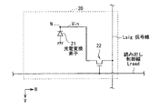
図3は、画素20の回路構成例を表したものである。画素20には、1つの光電変換素子21と、1つのトランジスタ22とが設けられている。この画素20にはまた、H方向に沿って延在する読み出し制御線Lreadと、V方向に沿って延在する信号線Lsigとが接続されている。
FIG. 3 illustrates a circuit configuration example of the
光電変換素子21は、例えばPIN(Positive Intrinsic Negative)型のフォトダイオードからなり、入射光(撮像光Lin)の光量に応じた電荷量の信号電荷を発生するようになっている。なお、この光電変換素子21のカソードは、蓄積ノードNに接続されている。
The
トランジスタ22は、読み出し制御線Lreadから供給される行走査信号に応じてオン状態となることにより、光電変換素子21で発生した信号電荷(入力電圧Vin)を信号線Lsigへ出力するトランジスタである。このトランジスタ22は、ここではNチャネル型(N型)の電界効果トランジスタ(FET)により構成されている。ただし、トランジスタ22がPチャネル型(P型)のFET等により構成されていてもよい。このトランジスタ22はまた、例えば、微結晶シリコンまたは多結晶シリコン等のシリコン系半導体を用いて構成されている。あるいは、酸化インジウムガリウム亜鉛(InGaZnO)または酸化亜鉛(ZnO)等の酸化物半導体を用いて構成してもよい。微結晶シリコン、多結晶シリコン(ポリシリコン)および酸化物半導体は、アモルファスシリコンに比べて移動度μが高いため、例えばトランジスタ22による信号の高速読み出しが可能になる。
The
この画素20では、トランジスタ22のゲートが読み出し制御線Lreadに接続され、ソースが信号線Lsigに接続され、ドレインが、光電変換素子21のカソード(蓄積ノードN)に接続されている。また、光電変換素子21のアノードは、グランド(接地)に接続されている。
In the
(静電気保護部18)
静電気保護部18は、ESD現象に起因した外部からの静電気入力に対して、内部の素子(具体的には、画素20内のトランジスタ22や光電変換素子21等)を保護する機能(ESD保護機能)を有している。具体的には、信号線Lsig等を介して入力する静電気に対して内部の素子を保護する役割を担っている。なお、ここでは、静電気保護部18が撮像領域(撮像部11)内に配設されている場合の例を示しているが、これには限られない。
(Static protection part 18)
The
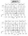
図4は、この静電気保護部18の回路構成例を表したものである。静電気保護部18は、H方向に沿って延在する複数の単位回路180(静電気保護回路)を有している。なお、ここでは便宜上、図中に示した6つの信号線を、Lsig1〜Lsig6として示している。
FIG. 4 shows a circuit configuration example of the
単位回路180は、信号線Lsig、グランド線Lgnd(接地線)および電源線(図示せず)からなる複数の配線のうちの、一の信号線Ligと他の一の配線との間に配設されている。具体的には、一の信号線Ligと他の一の信号線Ligとの間(隣接する一対の信号線Lsigの間)、一の信号線Lsigと一のグランド線Lgndとの間、または、一の信号線Lsigと一の電源線(図示せず)との間に、単位回路180が配設されている。図4に示した例では、信号線Lsig1,Lsig2の間、信号線Lsig2,Lsig3の間、信号線Lsig3,Lsig4の間、信号線Lsig4,Lsig5の間、および信号線Lsig5,Lsig6の間に、単位回路180が配設されている(本開示における「第1保護回路」の一具体例に対応)。また、信号線Lsig6とグランド線Lgndとの間に、単位回路180が配設されている(本開示における「第2保護回路」の一具体例に対応)。このように、図4に示した静電気保護部18では、複数の単位回路180(上記した「第1保護回路」および「第2保護回路」)が、隣接する複数の配線(ここでは、複数の信号線Lsig1〜Lsig6およびグランド線Lgnd等)の間で、連続的に(互いに隣り合って)配設されている。なお、上記したグランド線Lgndや電源線(図示せず)は、例えば撮像部11内の端部領域(例えばH方向に沿った右端部や左端部)に配設されている。
The
単位回路180は、1つのトランジスタTr1(第1のトランジスタ)と、1つの容量素子C1と、1つの抵抗素子R1とを有している。トランジスタTr1は、ここではNチャネル型(N型)のFETにより構成されている。なお、トランジスタTr1におけるゲート,ソース,ドレインはそれぞれ、図4中において「G」,「S」,「D」として示しており、以降の他の図においても同様である。各単位回路180にはまた、H方向に沿って延在する保護制御線Lctl1(第1の制御線)が接続されている。
The
この単位回路180では、トランジスタTr1のゲートが、抵抗素子R1を介して保護制御線Lctl1と間接的に接続されている。すなわち、抵抗素子R1の一端が保護制御線Lctl1に接続され、抵抗素子R1の他端がトランジスタTr1のゲートに接続されている。また、トランジスタTr1におけるソースおよびドレインのうちの一方(ここではドレイン)が、一の信号線Lsigおよび容量素子C1の一端に接続され、他方(ここではソース)が、前述した他の一の配線(ここでは信号線Lsigまたはグランド線Lgnd)に接続されている。容量素子C1の他端は、トランジスタTr1のゲートおよび抵抗素子R1の他端に接続されている。
In this
ここで、保護制御線Lctl1の電位Vctl1は、撮像装置1の電源(装置電源)がオン状態(装置動作状態)のときにトランジスタTr1がオフ状態となるように、設定されている。具体的には、例えば図5に示したように、トランジスタTr1におけるゲート−ソース間電圧Vgs<0を満たすように、保護制御線Lctl1の電位Vctl1が信号線Lsigの電位(信号電圧)Vsigよりも低く設定されている。また、例えば図6に示したように、信号線Lsigの電位Vsig(トランジスタTr1のソース電位に対応)が変化(ここでは、0V〜1Vの間で変化)した場合でもVgs<0を満たすように、保護制御線Lctl1の電位Vctl1(トランジスタTr1のゲート電位に対応)が設定されている。これにより、図5中の矢印P11で示したように、トランジスタTr1における閾値電圧Vthがマイナス側(負側)に多少変動した場合であっても、このトランジスタTr1におけるリーク電流(オフ状態のときの漏れ電流)を低く抑えることができる。したがって、装置電源がオン状態の際に、そのようなトランジスタTr1でのリーク電流に起因した各画素20からの信号(電荷)の読み出し動作への悪影響(電荷量の低減等)が抑えられるようになっている。つまり、画素20がいわゆるパッシブ型の回路構成(画素20内にソースフォロワ回路等のアンプが設けられていない構成)であっても、信号線Lsigにおける電位変動(電荷消失)が低減もしくは回避されるようになっている。
Here, the potential Vctl1 of the protection control line Lctl1 is set so that the transistor Tr1 is turned off when the power supply (device power supply) of the
図1に示した行走査部13は、例えばシフトレジスタやアドレスデコーダ等によって構成されており、撮像部11内の各画素20を例えば行単位で駆動する画素駆動部である。このような行単位での駆動は、上記した読み出し制御線Lreadを介して、上記した行走査信号を供給することによりなされる。
The
A/D変換部14は、図1に示したように、複数(ここでは4つ)の信号線Lsigごとに1つ設けられた複数の列選択部17を有しており、信号線Lsigを介して入力した信号電圧に基づいてA/D変換(アナログ/デジタル変換)を行うものである。また、各列選択部17は、例えば、アンプ、容量素子(コンデンサ)、スイッチ、サンプルホールド(S/H)回路、水平選択スイッチおよびA/Dコンバータ等(いずれも図示せず)を含んで構成されている。このような構成によりA/D変換部14では、デジタル信号からなる出力データDout(撮像信号)が生成され、外部へ出力されるようになっている。
As shown in FIG. 1, the A /
列走査部15は、例えばシフトレジスタやアドレスデコーダ等を含んで構成されており、上記した列選択部17内の各水平選択スイッチ(図示せず)を走査しつつ順番に駆動するものである。この列走査部15による選択走査により、信号線Lsigの各々を通して伝送される各画素20の信号(上記した出力データDout)が順番に出力されるようになっている。
The
システム制御部16は、上記した行走査部13、A/D変換部14および列走査部15等の動作を制御するものである。具体的には、システム制御部16は、各種のタイミング信号を生成するタイミングジェネレータを有しており、このタイミングジェネレータにおいて生成される各種のタイミング信号を基に、行走査部13、A/D変換部14および列走査部15等の駆動制御を行う。このようにして、システム制御部16の制御に基づいて、行走査部13、A/D変換部14および列走査部15がそれぞれ撮像部11内の複数の画素20に対する撮像駆動(順次走査)を行うことにより、撮像部11から出力データDoutが取得されるようになっている。
The
[撮像装置1の作用・効果]
(1.基本動作)
この撮像装置1では、図2に示したように撮像光Linが撮像部11へ入射すると、光電変換層111(図3に示した各画素20内の光電変換素子21)では、この撮像光Linが信号電荷に変換(光電変換)される。この光電変換によって発生した電荷により、蓄積ノードNでは蓄積ノード容量に応じた電圧変化が生じる。具体的には、蓄積ノード容量をCs、発生した電荷をqとすると、蓄積ノードNでは(q/Cs)の分だけ電圧が低下する。このような電圧変化に応じて、トランジスタ22のドレインには入力電圧Vin(光電変換素子21で発生した信号電荷)が印加される。このトランジスタ22へ供給される入力電圧Vinは、読み出し制御線Lreadから供給される行走査信号に応じてトランジスタ22がオン状態になると、その電荷が信号線Lsigへ出力される(読み出される)。
[Operation and Effect of Imaging Device 1]
(1. Basic operation)
In the
このようにして読み出された信号は、信号線Lsigを介して複数(ここでは4つ)の画素列ごとに、A/D変換部14内の列選択部17へ入力される。列選択部17では、まず、各信号線Lsigから入力される信号電荷ごとにチャージアンプ等においてQ−V変換を行い、信号電荷から信号電圧への変換を行う。次いで、変換された信号電圧ごとにA/D変換を行い、デジタル信号からなる出力データDout(撮像信号)を生成する。このようにして、各列選択部17から出力データDoutが順番に出力され、外部へ伝送される。
The signals read out in this way are input to the
(2.静電気保護部18の作用)
次に、本実施の形態における特徴部分の1つである、静電気保護部18(単位回路180)の作用について、比較例(比較例1,2)と比較しつつ詳細に説明する。
(2. Action of electrostatic protection unit 18)
Next, the operation of the electrostatic protection unit 18 (unit circuit 180), which is one of the characteristic parts in the present embodiment, will be described in detail in comparison with comparative examples (Comparative Examples 1 and 2).
(2−1.比較例1)
図7は、比較例1に係る静電気保護部の回路構成を表したものである。この比較例1の静電気保護部は、H方向に沿って延在する複数の単位回路108(静電気保護回路)を有している。
(2-1. Comparative Example 1)
FIG. 7 illustrates a circuit configuration of the electrostatic protection unit according to the first comparative example. The electrostatic protection unit of Comparative Example 1 includes a plurality of unit circuits 108 (electrostatic protection circuits) extending along the H direction.
単位回路108は、Nチャネル型(N型)のFETからなる2つのトランジスタTr101,102を有している。また、各単位回路108には、V方向に沿って延在する信号線Lsigと、H方向に沿って延在する電源線VDDおよび電源線VSS(グランド線)とが接続されている。この単位回路108では、トランジスタTr101のゲートおよびソースがともに信号線Lsigに接続され、トランジスタTr101のドレインが電源線VDDに接続されている。また、トランジスタTr102のゲートおよびソースがともに電源線VSSに接続され、トランジスタTr102のドレインが信号線Lsigに接続されている。このような回路構成により、トランジスタTr101,Tr102はそれぞれ、図中に破線で示した向きのダイオード(整流素子)として機能するようになっている。すなわち、アノードが電源線VDDに接続されると共にカソードが信号線Lsigに接続されたダイオードと、アノードが信号線Lsigに接続されると共にカソードが電源線VSSに接続されたダイオードとが配置されていることに相当する。
The
このような構成により単位回路108では、信号線Lsigに対して正電荷の静電気が入力すると、その静電気の電荷は、トランジスタTr101を介して電源線VDDへ放出される。また、信号線Lsigに対して負電荷の静電気が入力すると、その静電気の電荷は、トランジスタTr102を介して電源線VSSへ放出される。このようにして比較例1では、信号線Lsigを介して入力する静電気に対して内部の素子が保護されるようになっている。
With such a configuration, in the
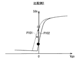
ところが、この比較例1の静電気保護部では、トランジスタTr101,Tr102においてそれぞれ、ソースとゲートとが互いに接続されており、常にVgs=0Vに設定されていることに起因して、以下の問題が生じる。すなわち、例えば図8中の矢印P101で示したように、トランジスタTr101,Tr102における閾値電圧Vthがマイナス側に多少でも変動すると、トランジスタTr101,Tr102におけるリーク電流が著しく増加してしまう(図8中の矢印P102参照)。このため、そのようなトランジスタTr1101,Tr102でのリーク電流に起因して、各画素20からの信号(電荷)の読み出し動作の際に、信号線Lsigにおける電位変動(電荷消失)が生じてしまう。このため、特に前述したパッシブ型の画素回路構成の場合、撮像画像において線欠陥等の画質劣化が発生してしまうことになる。
However, in the electrostatic protection unit of Comparative Example 1, the transistors Tr101 and Tr102 have the following problems caused by the fact that the source and the gate of the transistors Tr101 and Tr102 are connected to each other and are always set to Vgs = 0V. . That is, for example, as indicated by the arrow P101 in FIG. 8, if the threshold voltage Vth in the transistors Tr101 and Tr102 slightly varies to the minus side, the leakage current in the transistors Tr101 and Tr102 increases remarkably (in FIG. 8). (See arrow P102). For this reason, due to such a leakage current in the transistors Tr1101 and Tr102, a potential fluctuation (charge loss) in the signal line Lsig occurs during the signal (charge) read operation from each
また、この比較例1の静電気保護部では、各信号線Lsigと2つの電源線VDD,VSSとが交差していることから、以下の問題も生じる。すなわち、これらの配線間に形成される寄生容量Cp(図7中に破線で図示)が大きくなり、消費電力が増加したり、信号線Lsigにおける電圧波形がなまってしまったりする。 Further, in the electrostatic protection unit of Comparative Example 1, each signal line Lsig and the two power supply lines VDD and VSS intersect with each other, so that the following problem also occurs. That is, a parasitic capacitance Cp (shown by a broken line in FIG. 7) formed between these wirings increases, resulting in an increase in power consumption and a voltage waveform on the signal line Lsig being distorted.
(2−2.比較例2)
図9は、比較例2に係る静電気保護部の回路構成を表したものである。この比較例2の静電気保護部は、H方向に沿って延在する複数の単位回路208(静電気保護回路)を有している。各単位回路208には、V方向に沿って延在する複数の信号線(ここでは、3つの信号線Lsig201〜Lsig203を図示)と、H方向に沿って延在する1つの保護制御線Lctl1とが接続されている。また、各単位回路208は、隣接する一対の信号線間(ここでは、信号線Lsig201,Lsig202間および信号線Lsig202,Lsig203間)に配設されている。
(2-2. Comparative Example 2)
FIG. 9 illustrates a circuit configuration of the electrostatic protection unit according to the second comparative example. The electrostatic protection unit of Comparative Example 2 has a plurality of unit circuits 208 (electrostatic protection circuits) extending along the H direction. Each
単位回路208は、Nチャネル型(N型)のFETからなる1つのトランジスタTr201を有している。この単位回路208では、トランジスタTr201のゲートが保護制御線Lctl1に接続され、ソースが上記一対の信号線のうちの一方の信号線に接続され、ドレインが他方の信号線に接続されている。
The
このような構成により単位回路208では、例えば装置電源がオフ状態(装置停止状態)のときに、一方の信号線に対して負電荷の静電気が入力すると、Vgs>0となってトランジスタTr201がオン状態となることから、その静電気の電荷が他方の信号線側へ放出される。これにより比較例2では、信号線Lsigを介して入力する負電荷の静電気に対しては、内部の素子が保護されるようになっている。
With such a configuration, in the
ところが、例えば装置電源がオフ状態のときに、一方の信号線に対して正電荷の静電気が入力した場合には、Vgs<0のままである(Vgs>0とはならない)ことから、トランジスタTr201がオン状態とはならず、その静電気の電荷が他方の信号線側へ放出されない。すなわち、この比較例2の静電気保護部では、静電気が負電荷である場合には有効に動作する(内部の素子が有効に保護される)ものの、静電気が正電荷である場合には、有効に動作しない(内部の素子が有効に保護されない)。このように比較例2では、装置電源がオフ状態のときに、静電気からの有効な保護がなされない場合もあり得るのである。 However, for example, when positive charge static electricity is input to one of the signal lines when the device power is off, Vgs <0 remains (Vgs> 0 is not satisfied), so the transistor Tr201 Is not turned on, and the static charge is not released to the other signal line side. That is, the static electricity protection unit of Comparative Example 2 operates effectively when static electricity is negative charge (internal elements are effectively protected), but effective when static electricity is positive charge. Does not work (internal elements are not effectively protected). As described above, in Comparative Example 2, when the apparatus power supply is in the off state, effective protection from static electricity may not be achieved.
また、この比較例2の静電気保護部では、本実施の形態の静電気保護部18とは異なり、単位回路208のいずれもが一対の信号線間に配置されている(単位回路208が電源線やグランド線に接続されていない)ことから、以下の問題も生じ得る。すなわち、信号線を介して入力された静電気の電荷の最終的な放出経路が存在しないため、電界の放出効果(静電気からの保護機能)が不十分となり、場合によっては一部の素子が保護しきれないおそれがある。
Further, in the electrostatic protection unit of Comparative Example 2, unlike the
(2−3.本実施の形態)
これに対して本実施の形態では、図4に示した構成の複数の単位回路180が静電気保護部18内に設けられていることにより、各単位回路180では以下詳述する動作がなされ、その結果、上記比較例1,2と比べて静電気からの保護がより確実に行われる。
(2-3. This embodiment)
On the other hand, in the present embodiment, since the
(A.装置電源がオン状態のとき)
まず、装置電源がオン状態のときには、保護制御線Lctl1の電位Vctl1が、トランジスタTr1がオフ状態となるように設定されている。このため、例えば図10に示したように、装置電源がオン状態のときには、静電気保護部18内の各単位回路180では、トランジスタTr1が常にオフ状態となる。すなわち、装置電源がオン状態のときには、静電気保護部18は無効状態(非アクティブ状態)となる。ここで、図10および後述する図11,図12ではそれぞれ、便宜上、各トランジスタTr1をスイッチとして図示している。
(A. When the device power is on)
First, when the device power supply is in the on state, the potential Vctl1 of the protection control line Lctl1 is set so that the transistor Tr1 is in the off state. For this reason, as shown in FIG. 10, for example, when the apparatus power supply is in the on state, in each
(B.装置電源がオフ状態のとき)
一方、装置電源がオフ状態のときには、各信号線Lsigおよび保護制御線Lctl1がそれぞれフローティング状態となり、以下の図11および図12に示したように、静電気保護部18が有効状態(アクティブ状態)となる。また、撮像部11に対して何も接続されていない場合(例えば、撮像部11の製造工程中の場合)においても、同様のことが言える。なお、これらの図11および図12においては、便宜上、静電気保護部18内に図示した6つの単位回路180を、単位回路180−1〜180−6として示している。
(B. When the device power is off)
On the other hand, when the apparatus power supply is off, each signal line Lsig and protection control line Lctl1 are in a floating state, and as shown in FIGS. 11 and 12, the
(正電荷の静電気が入力した場合)
ここで、例えば図11(A)に示したように、信号線Lsig5を介して正電荷の静電気が入力すると(図中の矢印P21参照)、単位回路180−5内のトランジスタTr1において、ソース−ドレイン間の電圧Vds>0となる。また、それに伴い、容量素子C1による容量結合によって、トランジスタTr1のゲート電位も上昇し(図中の矢印P22参照)、ゲート−ソース間の電圧Vgs>0となる。したがって、この単位回路180−5内のトランジスタTr1が選択的にオン状態となり、信号線Lsig5を介して単位回路180−5内に入力した静電気の電荷(正電荷)が、トランジスタTr1のソース側(信号線Lsig6側)へと放出される(図中の矢印P21参照)。すなわち、隣接する2つの信号線Lsig5,Lsig6同士が、電気的に短絡状態(ショート状態)となる。また、このとき、単位回路180−5内の抵抗素子R1によって、トランジスタTr1のゲートと保護制御線Lctl1との電位差が一定期間保持されることから、トランジスタTr1が瞬時にオフしてしまう(オフ状態となってしまう)おそれが回避される。なお、このときトランジスタTr1が瞬時にオフしてしまうと、信号線Lsig5に入力した静電気の電荷を信号線Lsig6へ放出することができなくなってしまう。
(When positively charged static electricity is input)
Here, for example, as shown in FIG. 11A, when positively charged static electricity is input via the signal line Lsig5 (see the arrow P21 in the figure), the source − in the transistor Tr1 in the unit circuit 180-5. The drain-to-drain voltage Vds> 0. Accordingly, the gate potential of the transistor Tr1 also rises due to capacitive coupling by the capacitive element C1 (see arrow P22 in the figure), and the gate-source voltage Vgs> 0. Accordingly, the transistor Tr1 in the unit circuit 180-5 is selectively turned on, and the electrostatic charge (positive charge) input into the unit circuit 180-5 via the signal line Lsig5 is changed to the source side ( To the signal line Lsig6 side (see arrow P21 in the figure). That is, the two adjacent signal lines Lsig5 and Lsig6 are electrically short-circuited (short-circuited). At this time, the potential difference between the gate of the transistor Tr1 and the protection control line Lctl1 is held for a certain period by the resistance element R1 in the unit circuit 180-5, so that the transistor Tr1 is instantaneously turned off (OFF state). The risk of becoming) is avoided. At this time, if the transistor Tr1 is instantaneously turned off, the electrostatic charge input to the signal line Lsig5 cannot be discharged to the signal line Lsig6.
次いで、例えば図11(B)に示したように、信号線Lsig6側に放出された静電気の電荷(正電荷)は、単位回路180−5と隣接する単位回路180−6へ入力される(図中の矢印P23参照)。すると、この単位回路180−6においても、上記と同様にしてトランジスタTr1が選択的にオン状態となる。すなわち、Vds>0になると共に、容量素子C1による容量結合によってゲート電位も上昇し(図中の矢印P24参照)、Vgs>0となる。したがって、単位回路180−5側から単位回路180−6内に入力した静電気の電荷(正電荷)が、トランジスタTr1のソース側(グランド線Lgnd側)へと放出される(図中の矢印P23参照)。すなわち、隣接する信号線Lsig6およびグランド線Lgnd同士が電気的に短絡状態となり、静電気の電荷(正電荷)が最終的にグランド線Lgndへと放出される。このようにして、装置電源がオフ状態のときに信号線Lsigを介して正電荷の静電気が入力されると、静電気保護部18内の単位回路180において、次々に(順次に)トランジスタTr1がオン状態となり、最終的に電源線(図示せず)またはグランド線Lgndへと放出される。このとき、電荷が次々に分配されていくことから、電位は次第に低下していくことになる。その結果、上記比較例1,2と比べ、静電気からの保護がより確実に行われる。
Next, for example, as shown in FIG. 11B, the electrostatic charge (positive charge) discharged to the signal line Lsig6 side is input to the unit circuit 180-6 adjacent to the unit circuit 180-5 (FIG. 11B). (See arrow P23 in the middle). Then, also in this unit circuit 180-6, the transistor Tr1 is selectively turned on as described above. That is, Vds> 0, and the gate potential also rises due to capacitive coupling by the capacitive element C1 (see arrow P24 in the figure), and Vgs> 0. Therefore, the electrostatic charge (positive charge) input from the unit circuit 180-5 side into the unit circuit 180-6 is discharged to the source side (ground line Lgnd side) of the transistor Tr1 (see arrow P23 in the figure). ). That is, the adjacent signal line Lsig6 and the ground line Lgnd are electrically short-circuited, and static charges (positive charges) are finally discharged to the ground line Lgnd. In this way, when positively charged static electricity is input via the signal line Lsig when the apparatus power supply is off, the transistors Tr1 are turned on one after another in the
(負電荷の静電気が入力した場合)
一方、例えば図12(A)に示したように、信号線Lsig5を介して負電荷の静電気が入力すると(図中の矢印P31参照)、上記した正電荷の場合とは逆方向である単位回路180−4内のトランジスタTr1において、Vds>0かつVgs>0となる。したがって、この単位回路180−4内のトランジスタTr1が選択的にオン状態となり、信号線Lsig5を介して単位回路180−4内に入力した静電気の電荷(負電荷)が、トランジスタTr1のドレイン側(信号線Lsig4側)へと放出される(図中の矢印P31参照)。すなわち、隣接する2つの信号線Lsig5,Lsig4同士が、電気的に短絡状態となる。また、このときも単位回路180−4内の抵抗素子R1によって、トランジスタTr1のゲートと保護制御線Lctl1との電位差が一定期間保持されることから、トランジスタTr1が瞬時にオフしてしまうおそれが回避される。
(When negative static electricity is input)
On the other hand, for example, as shown in FIG. 12A, when negative charge static electricity is input via the signal line Lsig5 (see arrow P31 in the figure), the unit circuit is in the reverse direction to the case of the positive charge described above. In the transistor Tr1 in 180-4, Vds> 0 and Vgs> 0. Therefore, the transistor Tr1 in the unit circuit 180-4 is selectively turned on, and the electrostatic charge (negative charge) input into the unit circuit 180-4 via the signal line Lsig5 is changed to the drain side of the transistor Tr1 ( To the signal line Lsig4 side (see arrow P31 in the figure). That is, the two adjacent signal lines Lsig5 and Lsig4 are electrically short-circuited. Also at this time, the potential difference between the gate of the transistor Tr1 and the protection control line Lctl1 is held for a certain period by the resistance element R1 in the unit circuit 180-4, thereby avoiding the possibility of the transistor Tr1 being turned off instantaneously. Is done.
次いで、例えば図12(B)に示したように、信号線Lsig4側に放出された静電気の電荷(負電荷)は、単位回路180−4と隣接する単位回路180−3へ入力される(図中の矢印P32参照)。すると、この単位回路180−3においても、上記と同様にしてVds>0かつVgs>0となり、トランジスタTr1が選択的にオン状態となる。したがって、単位回路180−4側から単位回路180−3内に入力した静電気の電荷(負電荷)が、トランジスタTr1のドレイン側(信号線Lsig3側)へと放出される(図中の矢印P32参照)。すなわち、隣接する信号線Lsig4,Lsig3同士が電気的に短絡状態となる。なお、以降も同様の動作が連続的に行われることにより、静電気の電荷(負電荷)が、最終的に電源線(図示せず)またはグランド線Lgndへと放出される。このようにして、装置電源がオフ状態のときに信号線Lsigを介して負電荷の静電気が入力されると、静電気保護部18内の単位回路180において、次々に(順次に)トランジスタTr1がオン状態となり、最終的に電源線(図示せず)またはグランド線Lgndへと放出される。このときも電荷が次々に分配されていくことから、電位は次第に低下していくことになる。その結果、この場合も上記比較例1,2と比べ、静電気からの保護がより確実に行われる。
Next, for example, as shown in FIG. 12B, the electrostatic charge (negative charge) discharged to the signal line Lsig4 side is input to the unit circuit 180-3 adjacent to the unit circuit 180-4 (FIG. 12B). (See arrow P32 in the middle). Then, in this unit circuit 180-3 as well, Vds> 0 and Vgs> 0, and the transistor Tr1 is selectively turned on. Therefore, the electrostatic charge (negative charge) input from the unit circuit 180-4 side into the unit circuit 180-3 is discharged to the drain side (signal line Lsig3 side) of the transistor Tr1 (see arrow P32 in the figure). ). That is, the adjacent signal lines Lsig4 and Lsig3 are electrically short-circuited. Note that, since the same operation is continuously performed thereafter, electrostatic charges (negative charges) are finally discharged to the power supply line (not shown) or the ground line Lgnd. In this way, when negatively charged static electricity is input via the signal line Lsig when the apparatus power supply is off, the transistors Tr1 are turned on one after another in the
以上のように本実施の形態では、信号線Lsig、グランド線Lgnd(接地線)および電源線(図示せず)からなる複数の配線のうちの一の信号線Ligと他の一の配線との間に、単位回路180を有する静電気保護部18を設けるようにしたので、これらの配線のうちの一方の配線に対して正電荷または負電荷の静電気が入力された場合のいずれにおいても、他方の配線側にその静電気の電荷を放出することができる。よって、静電気からの保護をより確実に行うことが可能となり(静電耐圧を向上させることができ)、静電気による素子の特性変化を低減したり歩留まりを向上させることが可能となる。また、この静電気保護部18では、上記したように、静電気自身の電荷を利用してその静電気の電荷を放出させるようにしていることから、特殊なデバイスを別途設けることなく、静電耐圧を向上させることが可能となる。
As described above, in the present embodiment, one signal line Lig among the plurality of wirings including the signal line Lsig, the ground line Lgnd (grounding line), and the power supply line (not shown) is connected to the other wiring. Since the
また、装置電源がオン状態のときには、トランジスタTr1の閾値電圧Vth等がばらついてもリーク電流が小さくなるように制御されているため、各画素20からの信号(電荷)の読み出し動作の際に、信号線Lsigにおける電位変動(電荷消失)を抑えることができる。よって、画素20が前述したパッシブ型の回路構成であっても、撮像画像における線欠陥等の画質劣化の発生を低減することが可能となる。
Further, when the device power supply is in an on state, the leakage current is controlled to be small even if the threshold voltage Vth of the transistor Tr1 varies. Therefore, during the signal (charge) reading operation from each
更に、単位回路180内に抵抗素子R1を設けるようにしたので、トランジスタTr1のゲートと保護制御線Lctl1との電位差を一定期間保持することができ、トランジスタTr1が瞬時にオフしてしまうのを回避し、静電気保護部18をより確実に動作させることが可能となる。
Further, since the resistance element R1 is provided in the
加えて、複数の単位回路180が、隣接する複数の配線(ここでは、複数の信号線Lsig1〜Lsig6およびグランド線Lgnd等)の間で連続的に配設されているようにしたので、静電気の電荷を最終的に電源線(図示せず)またはグランド線Lgndへと放出することができ、静電気からの保護を更に確実に行うことが可能となる。
In addition, since the plurality of
<変形例>
続いて、上記実施の形態の変形例(変形例1〜6)について説明する。なお、実施の形態における構成要素と同一のものには同一の符号を付し、適宜説明を省略する。
<Modification>
Subsequently, modified examples (modified examples 1 to 6) of the above-described embodiment will be described. In addition, the same code | symbol is attached | subjected to the same thing as the component in embodiment, and description is abbreviate | omitted suitably.
[変形例1]
図13は、変形例1に係る静電気保護部(静電気保護部18A)の回路構成を表したものである。本変形例の静電気保護部18Aは、H方向に沿って延在する複数の単位回路180A(静電気保護回路)を有している。
[Modification 1]
FIG. 13 illustrates a circuit configuration of the electrostatic protection unit (
本変形例の単位回路180Aは、上記実施の形態の単位回路180において、Nチャネル型(N型)のFETからなるトランジスタTr1の代わりに、Pチャネル型(P型)のFETからなるトランジスタTr1を用いるようにしたものである。
In the
また、本変形例においても、保護制御線Lctl1の電位Vctl1は、装置電源がオン状態のときにトランジスタTr1がオフ状態となるように設定されている。具体的には、例えば図14に示したように、トランジスタTr1におけるゲート−ソース間電圧Vgs>0を満たすように、保護制御線Lctl1の電位Vctl1が信号線Lsigの電位(信号電圧)Vsigよりも高く設定されている。また、このときも、信号線Lsigの電位Vsigが変化した場合でもVgs>0を満たすように、保護制御線Lctl1の電位Vctl1が設定されている。これにより、図14中の矢印P41で示したように、トランジスタTr1における閾値電圧Vthがプラス側(正側)に多少変動した場合であっても、このトランジスタTr1におけるリーク電流(オフ状態のときの漏れ電流)を低く抑えることができる。したがって、本変形例においても上記実施の形態と同様に、装置電源がオン状態の際に、そのようなトランジスタTr1でのリーク電流に起因した各画素20からの信号(電荷)の読み出し動作への悪影響(電荷量の低減等)が抑えられるようになっている。
Also in this modification, the potential Vctl1 of the protection control line Lctl1 is set so that the transistor Tr1 is turned off when the device power supply is turned on. Specifically, for example, as shown in FIG. 14, the potential Vctl1 of the protection control line Lctl1 is higher than the potential (signal voltage) Vsig of the signal line Lsig so as to satisfy the gate-source voltage Vgs> 0 in the transistor Tr1. It is set high. Also at this time, the potential Vctl1 of the protection control line Lctl1 is set so as to satisfy Vgs> 0 even when the potential Vsig of the signal line Lsig changes. As a result, as indicated by an arrow P41 in FIG. 14, even when the threshold voltage Vth in the transistor Tr1 slightly fluctuates to the positive side (positive side), the leakage current (in the off state when the transistor Tr1 is off) (Leakage current) can be kept low. Therefore, in the present modification as well, in the same manner as in the above embodiment, when the apparatus power supply is in the on state, the signal (charge) read operation from each
このようにして本変形例においても、上記実施の形態と同様の作用により同様の効果を得ることが可能である。ただし、特にトランジスタTr1が多結晶半導体(多結晶シリコン等)を用いて構成されている場合、Pチャネル型よりもNチャネル型のほうが、一般にリーク電流が少ないことから、上記実施の形態のようにトランジスタTr1がNチャネル型であるほうが望ましいと言える。 Thus, also in this modification, it is possible to obtain the same effect by the same operation as the above embodiment. However, particularly when the transistor Tr1 is configured using a polycrystalline semiconductor (polycrystalline silicon or the like), the N-channel type generally has less leakage current than the P-channel type. It can be said that the transistor Tr1 is preferably an N-channel type.
[変形例2]
図15は、変形例2に係る静電気保護部(静電気保護部18B)の回路構成を表したものである。本変形例の静電気保護部18Bは、H方向に沿って延在する複数の単位回路180B(静電気保護回路)を有している。
[Modification 2]
FIG. 15 illustrates a circuit configuration of an electrostatic protection unit (electrostatic protection unit 18B) according to Modification 2. The electrostatic protection unit 18B according to the present modification includes a plurality of
本変形例の単位回路180Bは、上記実施の形態の単位回路180において、抵抗素子R1の代わりにトランジスタTr2(第2のトランジスタ)を設け、このトランジスタTr2が抵抗素子として機能するようにしたものとなっている。換言すると、この単位回路180Bでは、抵抗素子がトランジスタTr2により構成されている。また、各単位回路180Bには、これまで説明した保護制御線Lctl1に加え、H方向に沿って延在する保護制御線Lctl2(第2の制御線)もが接続されている。
The
この単位回路180Bでは、トランジスタTr1のゲートが、トランジスタTr2のドレインおよびソース(抵抗素子の一端および他端)を介して、保護制御線Lctl1と間接的に接続されている。すなわち、トランジスタTr2のソースが保護制御線Lctl1に接続され、トランジスタTr2のドレインがトランジスタTr1のゲートに接続されている。また、トランジスタTr2のゲートは、保護制御線Lctl2に接続されている。トランジスタTr1におけるソースおよびドレインのうちの一方(ここではドレイン)は、一の信号線Lsigおよび容量素子C1の一端に接続され、他方(ここではソース)が、前述した他の一の配線(ここでは信号線Lsigまたはグランド線Lgnd)に接続されている。容量素子C1の他端は、トランジスタTr1のゲートおよびトランジスタTr2のドレインに接続されている。
In the
また、本変形例では、上記した保護制御線Lctl2の電位は、装置電源がオン状態のときにトランジスタTr2がオン状態となるように設定されている。具体的には、トランジスタTr2におけるゲート−ソース間電圧Vgs>0を満たすように、保護制御線Lctl2の電位が設定されている。このようにして本変形例では、保護制御線Lctl2を用いて、装置電源がオン状態のときにトランジスタTr2が確実にオン状態となるように設定することが可能となっている。 In this modification, the potential of the protection control line Lctl2 is set so that the transistor Tr2 is turned on when the device power supply is turned on. Specifically, the potential of the protection control line Lctl2 is set so as to satisfy the gate-source voltage Vgs> 0 in the transistor Tr2. In this way, in this modification, the protection control line Lctl2 can be used to set the transistor Tr2 to be surely turned on when the device power supply is on.
このような構成により本変形例の静電気保護部18Bでは、装置電源がオン状態のときには、上記したように各単位回路180B内のトランジスタTr2がオン状態となるため、抵抗素子としての抵抗値が相対的に低くなる。したがって、撮像動作の際に信号電圧Vsigが変化し、容量素子C1による容量結合によってトランジスタTr1のゲート電位も変動した場合において、リーク電流が増大しないようにゲート電位を戻す作用を大きくすることが可能となる。
With this configuration, in the electrostatic protection unit 18B of the present modification, when the apparatus power supply is in the on state, the transistor Tr2 in each
一方、装置電源がオフ状態のときには、保護制御線Lctl2もフローティング状態となることから、上記とは逆にVgs≒0となるため、各単位回路180B内のトランジスタTr2がオフ状態となる。したがって、逆に抵抗素子としての抵抗値が相対的に高くなるため、トランジスタTr1が瞬時にオフしてしまうのをより確実に回避し、静電気保護部18Bをより確実に動作させることが可能となる。
On the other hand, since the protection control line Lctl2 is also in a floating state when the device power supply is in an off state, Vgs≈0, contrary to the above, so that the transistor Tr2 in each
なお、本変形例では、トランジスタTr1,Tr2がいずれもNチャネル型のFETにより構成されている場合について説明したが、例えば、これらのトランジスタTr1,Tr2のうちの少なくとも一方をPチャネル型のFETにより構成してもよい。 In this modification, the case where the transistors Tr1 and Tr2 are both N-channel FETs has been described. For example, at least one of the transistors Tr1 and Tr2 is formed of a P-channel FET. It may be configured.
[変形例3]
図16は、変形例3に係る静電気保護部(静電気保護部18C)の回路構成を表したものである。本変形例の静電気保護部18Cは、H方向に沿って延在する複数の単位回路180C(静電気保護回路)を有している。
[Modification 3]
FIG. 16 illustrates a circuit configuration of an electrostatic protection unit (
本変形例の単位回路180Cは、上記実施の形態の単位回路180において、抵抗素子R1を設けないようにした(省いた)ものであり、他の構成は同様となっている。これにより、各単位回路180Cでは、トランジスタTr1のゲートが、保護制御線Lctl1と直接接続されている。
The
このように、場合によっては、静電気保護部における各単位回路において抵抗素子を設けないようにしてもよい。ただし、前述したように、トランジスタTr1が瞬時にオフしてしまうのを回避し、静電気保護部をより確実に動作させることが可能となることから、抵抗素子を設けたほうが望ましいと言える。 In this way, depending on the case, the resistance element may not be provided in each unit circuit in the electrostatic protection unit. However, as described above, it can be said that it is desirable to provide a resistance element because the transistor Tr1 can be prevented from being turned off instantaneously and the electrostatic protection unit can be operated more reliably.
なお、本変形例では、トランジスタTr1がNチャネル型のFETにより構成されている場合について説明したが、例えば上記変形例1と同様に、トランジスタTr1をPチャネル型のFETにより構成してもよい。
In this modification, the case where the transistor Tr1 is configured by an N-channel FET has been described, but the transistor Tr1 may be configured by a P-channel FET, for example, as in the
[変形例4〜6]
図17(A)〜(C)はそれぞれ、変形例4〜6に係る撮像部(撮像部11A〜11C)の概略構成例を模式的に表したものである。
[
FIGS. 17A to 17C schematically illustrate schematic configuration examples of the imaging units (
まず、図17(A)に示した変形例4に係る撮像部11Aは、上記実施の形態の撮像部11における光電変換層111の代わりに、撮像素子112および縮小光学系113を有している。撮像素子112は、撮像光Linを検出して出力データDout(撮像信号)を取得する素子である。このような撮像素子112は、例えば、CCD(Charge-Coupled Devices)やCMOS(Complementary Metal-Oxide Semiconductor)等のイメージングセンサーを用いて構成することが可能である。縮小光学系113は、撮像素子112の受光面側に配設されており、例えばマイクロレンズアレイなどからなる。このような構成により、本変形例の撮像部11Aにおいても上記実施の形態の撮像部11と同様に、入射した撮像光Linに基づく情報の読み取りを行うことが可能となっている。
First, the
一方、図17(B)に示した変形例5に係る撮像部11Bは、上記実施の形態で説明した光電変換層111に加え、波長変換層114を更に有している。具体的には、光電変換層111上(撮像部11Bの受光側)に、波長変換層114が設けられている。また、図17(C)に示した変形例6に係る撮像部11Cは、上記変形例4で説明した撮像素子112および縮小光学系113に加え、波長変換層114を更に有している。具体的には、縮小光学系113上(撮像部11Cの受光側)に、波長変換層114が設けられている。
On the other hand, the imaging unit 11B according to the modified example 5 illustrated in FIG. 17B further includes a
波長変換層114は、放射線Rrad(α線,β線,γ線,X線等)を、光電変換層111または撮像素子112の感度域に波長変換するものであり、これにより光電変換層111および撮像素子112では、この放射線Rradに基づく情報を読み取ることが可能となっている。この波長変換層114は、例えばX線などの放射線を可視光に変換する蛍光体(例えば、シンチレータ)からなる。このような波長変換層114は、例えば光電変換層111または縮小光学系113の上部に、有機平坦化膜、スピンオングラス材料等からなる平坦化膜を形成し、その上部に蛍光体膜をCsI、NaI、CaF2等によって形成することにより得られる。
The
このような構成の撮像部11B,11Cを備えた変形例5,6に係る撮像装置では、撮像部11B,11Cが、入射した放射線Rradに応じて電気信号を発生するものとなっており、放射線撮像装置として構成されている。このような放射線撮像装置は、例えば医療機器(Digital Radiography等のX線撮像装置)や、空港等で用いられる携帯物検査用X線撮影装置、工業用X線撮像装置(例えば、コンテナ内の危険物等の検査や、鞄等の中身の検査を行う装置)などに適用することが可能である。 In the imaging devices according to the modified examples 5 and 6 including the imaging units 11B and 11C having such a configuration, the imaging units 11B and 11C generate an electrical signal according to the incident radiation Rrad, and the radiation It is configured as an imaging device. Such a radiation imaging apparatus is, for example, a medical device (an X-ray imaging apparatus such as Digital Radiography), an X-ray imaging apparatus for portable object inspection used in an airport or the like, an industrial X-ray imaging apparatus (for example, a danger in a container). The present invention can be applied to an apparatus for inspecting objects and the like, and inspecting contents of bags and the like.
<適用例>
続いて、上記実施の形態および各変形例(変形例1〜6)に係る撮像装置の撮像表示システムへの適用例について説明する。
<Application example>
Next, application examples of the imaging device according to the above-described embodiment and each modification (
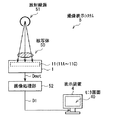
図18は、適用例に係る撮像表示システム(撮像表示システム5)の概略構成例を模式的に表したものである。この撮像表示システム5は、上記実施の形態等に係る撮像部11(11A〜11C)等を有する撮像装置1と、画像処理部52と、表示装置4とを備えており、この例では放射線を用いた撮像表示システムとして構成されている。
FIG. 18 schematically illustrates a schematic configuration example of an imaging display system (imaging display system 5) according to an application example. The imaging display system 5 includes the
画像処理部52は、撮像装置1から出力される出力データDout(撮像信号)に対して所定の画像処理を施すことにより、画像データD1を生成するものである。表示装置4は、画像処理部52において生成された画像データD1に基づく画像表示を、所定のモニタ画面40上で行うものである。
The
このような構成からなる撮像表示システム5では、撮像装置1(ここでは放射線撮像装置)が、放射線源(例えばX線源)51から被写体50に向けて照射された放射線に基づき、被写体50の画像データDoutを取得し、画像処理部52へ出力する。画像処理部52は、入力された画像データDoutに対して上記した所定の画像処理を施し、その画像処理後の画像データ(表示データ)D1を表示装置4へ出力する。表示装置4は、入力された画像データD1に基づいて、モニタ画面40上に画像情報(撮像画像)を表示する。
In the imaging display system 5 having such a configuration, the imaging device 1 (here, the radiation imaging device) is based on radiation emitted from a radiation source (for example, an X-ray source) 51 toward the subject 50, and an image of the subject 50 is displayed. Data Dout is acquired and output to the
このように、本適用例の撮像表示システム5では、撮像装置1において被写体50の画像を電気信号として取得可能であるため、取得した電気信号を表示装置4へ伝送することで、画像表示を行うことができる。すなわち、従来のような放射線写真フィルムを用いることなく、被写体50の画像を観察することが可能となり、また、動画撮影および動画表示にも対応することが可能となる。
As described above, in the imaging display system 5 of this application example, the image of the subject 50 can be acquired as an electrical signal in the
なお、本適用例では、撮像装置1が放射線撮像装置として構成されており、放射線を用いた撮像表示システムとなっている場合を例に挙げて説明したが、本開示の撮像表示システムは、他の方式の撮像装置を用いたものにも適用することが可能である。
In this application example, the case where the
<その他の変形例>
以上、実施の形態、変形例および適用例を挙げて本技術を説明したが、本技術はこれらの実施の形態等に限定されず、種々の変形が可能である。
<Other variations>
Although the present technology has been described with the embodiment, the modification, and the application example, the present technology is not limited to the embodiment and the like, and various modifications can be made.
例えば、上記実施の形態等では、静電気保護部内に単位回路(静電気保護回路)が複数設けられている場合について説明したが、これには限られず、静電気保護部内に単位回路が1つだけ設けられているようにしてもよい。 For example, in the above embodiment, the case where a plurality of unit circuits (electrostatic protection circuits) are provided in the electrostatic protection unit has been described. However, the present invention is not limited to this, and only one unit circuit is provided in the electrostatic protection unit. You may be allowed to.
また、撮像部における画素の回路構成は、上記実施の形態等で説明したもの(画素20の回路構成)には限られず、他の回路構成であってもよい。すなわち、例えば、光電変換素子21のアノードが蓄積ノードNに接続されていると共に、カソードが電源VDDに接続されているようにしてもよい。また、例えば画素内に、所定のソースフォロワ回路が設けられているようにしてもよい。
In addition, the circuit configuration of the pixel in the imaging unit is not limited to the one described in the above embodiment and the like (the circuit configuration of the pixel 20), and may be another circuit configuration. That is, for example, the anode of the
更に、上記実施の形態等で説明した撮像部11、行走査部13、A/D変換部14(列選択部17)、列走査部15および静電気保護部18はそれぞれ、同一基板上に形成されているようにしてもよい。具体的には、例えば低温多結晶シリコン(Si)などの多結晶半導体を用いることにより、これらの回路部分におけるスイッチ等も同一基板上に形成することができるため、例えば外部のシステム制御部16からの制御信号に基づいて同一基板上における駆動動作が可能となる。
Furthermore, the
加えて、上記実施の形態等では、本技術における「信号伝達装置」の一例として、複数の画素(撮像画素)が信号の入力動作(撮像動作)を行う撮像装置を挙げて説明したが、これには限られない。すなわち、上記実施の形態等で説明した静電気保護部(静電気保護回路)は、複数の画素において信号の入力動作(撮像動作)および出力動作(表示動作)のうちの少なくとも一方の動作を行う信号伝達装置において適用することが可能である。 In addition, in the above-described embodiment and the like, as an example of the “signal transmission device” in the present technology, an imaging device in which a plurality of pixels (imaging pixels) perform a signal input operation (imaging operation) has been described. It is not limited to. That is, the electrostatic protection unit (electrostatic protection circuit) described in the above embodiments and the like transmits a signal that performs at least one of a signal input operation (imaging operation) and an output operation (display operation) in a plurality of pixels. It can be applied in the apparatus.
具体的には、例えば図19に示した表示装置3(信号伝達装置)では、複数の画素60(表示画素)が信号の出力動作(表示動作)を行うようになっている。この表示装置3は、複数の画素60を有する表示部31と、信号線Lsigに対して映像信号を供給する信号線駆動部32(データドライバ)と、書き込み制御線Lwrite(ゲート線)をV方向に順次走査する行走査部33(ゲートドライバ)と、システム制御部34とを備えている。表示装置3にはまた、上記実施の形態等で説明した静電気保護部18(18A〜18C)が設けられている。システム制御部34は、信号線駆動部32および行走査部33の動作を制御するものである。また、各画素60には、表示素子61(例えば液晶素子や有機EL(Electro Luminescence)素子等)と、スイッチング素子としてのトランジスタ62とが設けられ、信号線Lsigおよび書き込み制御線Lwriteが接続されている。このような構成の表示装置3においても、上記実施の形態と同様の作用により同様の効果を得ることが可能である。
Specifically, for example, in the display device 3 (signal transmission device) illustrated in FIG. 19, a plurality of pixels 60 (display pixels) perform a signal output operation (display operation). The
なお、本技術は以下のような構成を取ることも可能である。
(1)
信号の入力動作および出力動作のうちの少なくとも一方の動作を行う複数の画素と、
前記画素に接続された1または複数の信号線と、
前記信号線を含む複数の配線と、
前記複数の配線のうちの一の信号線と他の一の配線との間に配設され、第1トランジスタおよび容量素子を有する1または複数の静電気保護回路と、
前記静電気保護回路に接続された第1制御線と
を備え、
前記静電気保護回路では、
前記第1トランジスタのゲートが、前記第1制御線と直接もしくは間接的に接続され、
前記第1トランジスタにおけるソースおよびドレインのうちの一方が、前記一の信号線および前記容量素子の一端に接続されると共に、他方が前記他の一の配線に接続され、
前記容量素子の他端が、前記第1トランジスタのゲートに接続されている
信号伝達装置。
(2)
前記静電気保護回路は、抵抗素子を更に有し、
前記抵抗素子の一端は、前記第1制御線に接続され、
前記抵抗素子の他端は、前記第1トランジスタのゲートおよび前記容量素子の他端に接続されている。
上記(1)に記載の信号伝達装置。
(3)
前記抵抗素子が、第2トランジスタにより構成されている
上記(2)に記載の信号伝達装置。
(4)
前記抵抗素子の一端および他端が、前記第2トランジスタのソースまたはドレインであり、
前記第2トランジスタのゲートには、第2制御線が接続されている
上記(3)に記載の信号伝達装置。
(5)
装置電源がオン状態のときに前記第2トランジスタがオン状態となるように、前記第2制御線の電位が設定されている
上記(4)に記載の信号伝達装置。
(6)
装置電源がオン状態のときに前記第1トランジスタがオフ状態となるように、前記第1制御線の電位が設定されている
上記(1)ないし(5)のいずれか1項に記載の信号伝達装置。
(7)
前記他の一の配線が、前記複数の配線のうちの、他の一の信号線、一の電源線または一の接地線である
上記(1)ないし(6)のいずれか1項に記載の信号伝達装置。
(8)
前記複数の静電気保護回路が、
前記一の信号線と前記他の一の信号線との間に配設された、1または複数の第1保護回路と、
前記一の信号線と、前記一の電源線または前記一の接地線との間に配設された、1または複数の第2保護回路とからなる
上記(7)に記載の信号伝達装置。
(9)
前記第1保護回路および前記第2保護回路が、隣接する複数の配線間で連続的に配設されている
上記(8)に記載の信号伝達装置。
(10)
前記複数の画素は、信号の入力動作としての撮像動作を行うものであり、撮像装置として構成されている
上記(1)ないし(9)のいずれか1項に記載の信号伝達装置。
(11)
前記複数の画素は、前記撮像動作として、入射した放射線に応じて電気信号を発生するものであり、放射線撮像装置として構成されている
上記(10)に記載の信号伝達装置。
(12)
前記放射線がX線である
上記(11)に記載の信号伝達装置。
(13)
前記複数の画素は、信号の出力動作としての表示動作を行うものであり、表示装置として構成されている
上記(1)ないし(9)のいずれか1項に記載の信号伝達装置。
(14)
撮像装置と、この撮像装置により得られた撮像信号に基づく画像表示を行う表示装置とを備え、
前記撮像装置は、
撮像動作を行う複数の画素と、
前記画素に接続された1または複数の信号線と、
前記信号線を含む複数の配線と、
前記複数の配線のうちの一の信号線と他の一の配線との間に配設され、第1トランジスタおよび容量素子を有する1または複数の静電気保護回路と、
前記静電気保護回路に接続された第1制御線と
を備え、
前記静電気保護回路では、
前記第1トランジスタのゲートが、前記第1制御線と直接もしくは間接的に接続され、
前記第1トランジスタにおけるソースおよびドレインのうちの一方が、前記一の信号線および前記容量素子の一端に接続されると共に、他方が前記他の一の配線に接続され、
前記容量素子の他端が、前記第1トランジスタのゲートに接続されている
撮像表示システム。
In addition, this technique can also take the following structures.
(1)
A plurality of pixels that perform at least one of a signal input operation and an output operation;
One or more signal lines connected to the pixel;
A plurality of wires including the signal lines;
One or a plurality of electrostatic protection circuits disposed between one signal line and the other one of the plurality of wirings and having a first transistor and a capacitor;
A first control line connected to the electrostatic protection circuit,
In the electrostatic protection circuit,
A gate of the first transistor is directly or indirectly connected to the first control line;
One of a source and a drain in the first transistor is connected to one signal line and one end of the capacitor, and the other is connected to the other wiring.
The other end of the capacitive element is connected to the gate of the first transistor.
(2)
The electrostatic protection circuit further includes a resistance element,
One end of the resistance element is connected to the first control line,
The other end of the resistive element is connected to the gate of the first transistor and the other end of the capacitive element.
The signal transmission device according to (1) above.
(3)
The signal transmission device according to (2), wherein the resistance element includes a second transistor.
(4)
One end and the other end of the resistive element are the source or drain of the second transistor,
The signal transmission device according to (3), wherein a second control line is connected to a gate of the second transistor.
(5)
The signal transmission device according to (4), wherein the potential of the second control line is set so that the second transistor is turned on when the device power supply is turned on.
(6)
The signal transmission according to any one of (1) to (5), wherein the potential of the first control line is set so that the first transistor is turned off when the apparatus power supply is on. apparatus.
(7)
The other one wiring is one other signal line, one power supply line, or one grounding line among the plurality of wirings, according to any one of (1) to (6) above. Signal transmission device.
(8)
The plurality of electrostatic protection circuits are
One or more first protection circuits disposed between the one signal line and the other signal line;
The signal transmission device according to (7), including the one signal line and one or a plurality of second protection circuits disposed between the one power line or the one ground line.
(9)
The signal transmission device according to (8), wherein the first protection circuit and the second protection circuit are continuously disposed between a plurality of adjacent wirings.
(10)
The signal transmission device according to any one of (1) to (9), wherein the plurality of pixels perform an imaging operation as a signal input operation and are configured as an imaging device.
(11)
The signal transmission device according to (10), wherein the plurality of pixels generate an electrical signal in accordance with incident radiation as the imaging operation, and are configured as a radiation imaging device.
(12)
The signal transmission device according to (11), wherein the radiation is X-rays.
(13)
The signal transmission device according to any one of (1) to (9), wherein the plurality of pixels perform display operation as signal output operation and are configured as a display device.
(14)
An imaging device, and a display device that displays an image based on an imaging signal obtained by the imaging device,
The imaging device
A plurality of pixels that perform imaging operations;
One or more signal lines connected to the pixel;
A plurality of wires including the signal lines;
One or a plurality of electrostatic protection circuits disposed between one signal line and the other one of the plurality of wirings and having a first transistor and a capacitor;
A first control line connected to the electrostatic protection circuit,
In the electrostatic protection circuit,
A gate of the first transistor is directly or indirectly connected to the first control line;
One of a source and a drain in the first transistor is connected to one signal line and one end of the capacitor, and the other is connected to the other wiring.
The imaging display system, wherein the other end of the capacitive element is connected to the gate of the first transistor.
1…撮像装置(信号伝達装置)、11,11A〜11C…撮像部、111…光電変換層、112…撮像素子、113…縮小光学系、114…波長変換層、13…行走査部、14…A/D変換部、15…列選択部、16…システム制御部、17…列選択部、18,18A〜18C…静電気保護部、180,180−1〜180−6,180A〜180C…単位回路(静電気保護回路)、20…画素(撮像画素)、21…光電変換素子、22…トランジスタ、3…表示装置(信号伝達装置)、31…表示部、32…信号線駆動部、33…行走査部、34…システム制御部、4…表示装置、40…モニタ画面、5…撮像表示システム、50…被写体、51…放射線源、52…画像処理部、60…画素(表示画素)、61…表示素子、62…トランジスタ、Vin…入力電圧、Lread…読み出し制御線、Lsig,Lsig1〜Lsig6…信号線、Lgnd…グランド線(接地線)、Lctl1,Lctl2…保護制御線、Lwrite…書き込み制御線(ゲート線)、Dout…出力データ(撮像信号)、D1…撮像信号、N…蓄積ノード、Lin…撮像光、Rrad…放射線、Tr1,Tr2…トランジスタ、C1…容量素子、R1…抵抗素子。
DESCRIPTION OF
Claims (12)
前記画素に接続された1または複数の信号線と、
前記信号線を含む複数の配線と、
前記複数の配線のうちの一の信号線と他の一の配線との間に配設され、第1トランジスタと、容量素子と、第2トランジスタにより構成された抵抗素子とを有する1または複数の静電気保護回路と、
前記静電気保護回路に接続された第1制御線と
を備え、
前記静電気保護回路では、
前記第1トランジスタのゲートが、前記第1制御線と直接もしくは間接的に接続され、
前記第1トランジスタにおけるソースおよびドレインのうちの一方が、前記一の信号線および前記容量素子の一端に接続されると共に、他方が前記他の一の配線に接続され、
前記容量素子の他端が、前記第1トランジスタのゲートに接続され、
前記抵抗素子の一端が、前記第1制御線に接続され、
前記抵抗素子の他端が、前記第1トランジスタのゲートおよび前記容量素子の他端に接続されている
信号伝達装置。 A plurality of pixels that perform at least one of a signal input operation and an output operation;
One or more signal lines connected to the pixel;
A plurality of wires including the signal lines;
One or a plurality of ones having a first transistor , a capacitive element, and a resistance element constituted by a second transistor , disposed between one signal line and the other one of the plurality of wirings An electrostatic protection circuit,
A first control line connected to the electrostatic protection circuit,
In the electrostatic protection circuit,
A gate of the first transistor is directly or indirectly connected to the first control line;
One of a source and a drain in the first transistor is connected to one signal line and one end of the capacitor, and the other is connected to the other wiring.
The other end of the capacitive element is connected to the gate of the first transistor ;
One end of the resistance element is connected to the first control line,
A signal transmission device in which the other end of the resistive element is connected to the gate of the first transistor and the other end of the capacitive element .
前記第2トランジスタのゲートには、第2制御線が接続されている
請求項1に記載の信号伝達装置。 One end and the other end of the resistive element are the source or drain of the second transistor,
The signal transmission device according to claim 1 , wherein a second control line is connected to a gate of the second transistor.
請求項2に記載の信号伝達装置。 As the device power supply is the second transistor is turned on when the on state, the signal transmission apparatus according to claim 2 in which the potential of the second control line is set.
請求項1ないし請求項3のいずれか1項に記載の信号伝達装置。 The signal transmission device according to any one of claims 1 to 3 , wherein the potential of the first control line is set so that the first transistor is turned off when the device power supply is on. .
請求項1ないし請求項4のいずれか1項に記載の信号伝達装置。 Said other one wiring, among the plurality of wirings, other one of the signal lines, the signal according to any one of one claims 1 to 4 as a power supply line or a ground line Transmission device.
前記一の信号線と前記他の一の信号線との間に配設された、1または複数の第1保護回路と、
前記一の信号線と、前記一の電源線または前記一の接地線との間に配設された、1または複数の第2保護回路とからなる
請求項5に記載の信号伝達装置。 The plurality of electrostatic protection circuits are
One or more first protection circuits disposed between the one signal line and the other signal line;
The signal transmission device according to claim 5 , comprising: the one signal line and one or a plurality of second protection circuits disposed between the one power supply line or the one ground line.
請求項6に記載の信号伝達装置。 The signal transmission device according to claim 6 , wherein the first protection circuit and the second protection circuit are continuously disposed between a plurality of adjacent wirings.
請求項1ないし請求項7のいずれか1項に記載の信号伝達装置。 Wherein the plurality of pixels is for performing an imaging operation as an input operation of the signal, the signal transmission device according to any one of claims 1 to 7 is configured as an imaging device.
請求項8に記載の信号伝達装置。 The signal transmission device according to claim 8 , wherein the plurality of pixels generate an electrical signal according to incident radiation as the imaging operation, and are configured as a radiation imaging device.
請求項9に記載の信号伝達装置。 The signal transmission device according to claim 9 , wherein the radiation is an X-ray.
請求項1ないし請求項7のいずれか1項に記載の信号伝達装置。 Wherein the plurality of pixels, which perform a display operation as the output operation of the signal, the signal transmission device according to any one of claims 1 to 7 is configured as a display device.
前記撮像装置は、
撮像動作を行う複数の画素と、
前記画素に接続された1または複数の信号線と、
前記信号線を含む複数の配線と、
前記複数の配線のうちの一の信号線と他の一の配線との間に配設され、第1トランジスタと、容量素子と、第2トランジスタにより構成された抵抗素子とを有する1または複数の静電気保護回路と、
前記静電気保護回路に接続された第1制御線と
を備え、
前記静電気保護回路では、
前記第1トランジスタのゲートが、前記第1制御線と直接もしくは間接的に接続され、
前記第1トランジスタにおけるソースおよびドレインのうちの一方が、前記一の信号線および前記容量素子の一端に接続されると共に、他方が前記他の一の配線に接続され、
前記容量素子の他端が、前記第1トランジスタのゲートに接続され、
前記抵抗素子の一端が、前記第1制御線に接続され、
前記抵抗素子の他端が、前記第1トランジスタのゲートおよび前記容量素子の他端に接続されている
撮像表示システム。 An imaging device, and a display device that displays an image based on an imaging signal obtained by the imaging device,
The imaging device
A plurality of pixels that perform imaging operations;
One or more signal lines connected to the pixel;
A plurality of wires including the signal lines;
One or a plurality of ones having a first transistor , a capacitive element, and a resistance element constituted by a second transistor , disposed between one signal line and the other one of the plurality of wirings An electrostatic protection circuit,
A first control line connected to the electrostatic protection circuit,
In the electrostatic protection circuit,
A gate of the first transistor is directly or indirectly connected to the first control line;
One of a source and a drain in the first transistor is connected to one signal line and one end of the capacitor, and the other is connected to the other wiring.
The other end of the capacitive element is connected to the gate of the first transistor ;
One end of the resistance element is connected to the first control line,
An imaging display system in which the other end of the resistive element is connected to the gate of the first transistor and the other end of the capacitive element .
Priority Applications (5)
| Application Number | Priority Date | Filing Date | Title |
|---|---|---|---|
| JP2011114827A JP5724623B2 (en) | 2011-05-23 | 2011-05-23 | Signal transmission device and imaging display system |
| TW101115862A TWI545717B (en) | 2011-05-23 | 2012-05-03 | Signal transmission apparatus and imaging display system |
| US13/468,403 US8970463B2 (en) | 2011-05-23 | 2012-05-10 | Signal transmission apparatus and imaging display system |
| KR1020120051311A KR101951486B1 (en) | 2011-05-23 | 2012-05-15 | Signal transmission apparatus and imaging display system |
| CN201210152327.1A CN102801902B (en) | 2011-05-23 | 2012-05-16 | Signal transmission device and imaging display system |
Applications Claiming Priority (1)
| Application Number | Priority Date | Filing Date | Title |
|---|---|---|---|
| JP2011114827A JP5724623B2 (en) | 2011-05-23 | 2011-05-23 | Signal transmission device and imaging display system |
Publications (3)
| Publication Number | Publication Date |
|---|---|
| JP2012244053A JP2012244053A (en) | 2012-12-10 |
| JP2012244053A5 JP2012244053A5 (en) | 2014-06-19 |
| JP5724623B2 true JP5724623B2 (en) | 2015-05-27 |
Family
ID=47200858
Family Applications (1)
| Application Number | Title | Priority Date | Filing Date |
|---|---|---|---|
| JP2011114827A Active JP5724623B2 (en) | 2011-05-23 | 2011-05-23 | Signal transmission device and imaging display system |
Country Status (5)
| Country | Link |
|---|---|
| US (1) | US8970463B2 (en) |
| JP (1) | JP5724623B2 (en) |
| KR (1) | KR101951486B1 (en) |
| CN (1) | CN102801902B (en) |
| TW (1) | TWI545717B (en) |
Families Citing this family (7)
| Publication number | Priority date | Publication date | Assignee | Title |
|---|---|---|---|---|
| KR102000738B1 (en) * | 2013-01-28 | 2019-07-23 | 삼성디스플레이 주식회사 | Circuit for preventing static electricity and display device comprising the same |
| JP2014195243A (en) * | 2013-02-28 | 2014-10-09 | Semiconductor Energy Lab Co Ltd | Semiconductor device |
| JP6202840B2 (en) * | 2013-03-15 | 2017-09-27 | キヤノン株式会社 | Radiation imaging apparatus, radiation imaging system, control method and program for radiation imaging apparatus |
| CN104090436B (en) * | 2014-06-26 | 2017-03-22 | 京东方科技集团股份有限公司 | Gate line drive circuit of array substrate and display device |
| CN109285510B (en) * | 2018-09-11 | 2021-04-02 | 重庆惠科金渝光电科技有限公司 | Display, display device and grounding resistance adjusting method |
| CN112509467B (en) * | 2020-11-27 | 2022-03-08 | 合肥维信诺科技有限公司 | Display substrate, electrostatic discharge device and method |
| WO2023155090A1 (en) * | 2022-02-17 | 2023-08-24 | Jade Bird Display (shanghai) Limited | Electrostatic discharge protection system of a micro device |
Family Cites Families (12)
| Publication number | Priority date | Publication date | Assignee | Title |
|---|---|---|---|---|
| US6337722B1 (en) * | 1997-08-07 | 2002-01-08 | Lg.Philips Lcd Co., Ltd | Liquid crystal display panel having electrostatic discharge prevention circuitry |
| GB0119299D0 (en) | 2001-08-08 | 2001-10-03 | Koninkl Philips Electronics Nv | Electrostatic discharge protection for pixellated electronic device |
| JP4000096B2 (en) * | 2003-08-04 | 2007-10-31 | 株式会社東芝 | ESD protection circuit |
| JP2006065284A (en) * | 2004-07-26 | 2006-03-09 | Seiko Epson Corp | Light-emitting device and electronic apparatus |
| JP5252817B2 (en) * | 2006-03-29 | 2013-07-31 | キヤノン株式会社 | Imaging device, radiation imaging device, driving method of imaging device, radiation imaging system, and manufacturing method of imaging device |
| JP4142066B2 (en) * | 2006-06-01 | 2008-08-27 | エプソンイメージングデバイス株式会社 | Electro-optical device and electronic apparatus |
| KR101304416B1 (en) * | 2006-11-10 | 2013-09-05 | 삼성디스플레이 주식회사 | Liquid crystal display device and manufacturing method thereof |
| JP2008233417A (en) * | 2007-03-19 | 2008-10-02 | Toshiba Matsushita Display Technology Co Ltd | Matrix array substrate and flat panel display device using the same |
| TWI357146B (en) * | 2008-04-07 | 2012-01-21 | Chunghwa Picture Tubes Ltd | Flat display panel |
| JP2009302092A (en) * | 2008-06-10 | 2009-12-24 | Epson Imaging Devices Corp | Solid-state imaging device |
| KR101362015B1 (en) * | 2008-12-24 | 2014-02-11 | 엘지디스플레이 주식회사 | Flat Panel Display Comprising Static Electricity Protection Circuit |
| KR101255289B1 (en) * | 2009-12-31 | 2013-04-15 | 엘지디스플레이 주식회사 | Liquid crystal display device |
-
2011
- 2011-05-23 JP JP2011114827A patent/JP5724623B2/en active Active
-
2012
- 2012-05-03 TW TW101115862A patent/TWI545717B/en not_active IP Right Cessation
- 2012-05-10 US US13/468,403 patent/US8970463B2/en not_active Expired - Fee Related
- 2012-05-15 KR KR1020120051311A patent/KR101951486B1/en active IP Right Grant
- 2012-05-16 CN CN201210152327.1A patent/CN102801902B/en not_active Expired - Fee Related
Also Published As
| Publication number | Publication date |
|---|---|
| CN102801902A (en) | 2012-11-28 |
| US20120299804A1 (en) | 2012-11-29 |
| KR20120130700A (en) | 2012-12-03 |
| CN102801902B (en) | 2017-05-17 |
| TWI545717B (en) | 2016-08-11 |
| TW201304110A (en) | 2013-01-16 |
| KR101951486B1 (en) | 2019-02-22 |
| US8970463B2 (en) | 2015-03-03 |
| JP2012244053A (en) | 2012-12-10 |
Similar Documents
| Publication | Publication Date | Title |
|---|---|---|
| JP5724623B2 (en) | Signal transmission device and imaging display system | |
| US9277153B2 (en) | Image pickup device and image pickup display system | |
| US8424764B2 (en) | Photoelectric conversion device, method for driving photoelectric conversion device, radiation imaging device, and method for driving radiation imaging device | |
| US9357143B2 (en) | Image pickup unit and image pickup display system | |
| JP5935293B2 (en) | Imaging apparatus and imaging display system | |
| KR101966991B1 (en) | Image pickup unit and image-pickup and display system | |
| JP5874670B2 (en) | Imaging apparatus and imaging display system | |
| US9196647B2 (en) | Image pickup unit and image pickup display system | |
| US9019425B2 (en) | Image pickup unit and image pickup display system | |
| JP5895650B2 (en) | Imaging apparatus and imaging display system | |
| JP2013247270A (en) | Imaging device and imaging display system | |
| JP5935291B2 (en) | Imaging apparatus and imaging display system | |
| JP2013090219A (en) | Imaging apparatus and imaging display system | |
| US20140291670A1 (en) | Image pickup device and image pickup display system | |
| JP5974654B2 (en) | Imaging apparatus and imaging display system | |
| US20100214460A1 (en) | Solid-state imaging device | |
| JP5817227B2 (en) | Radiation imaging apparatus and radiation imaging display system |
Legal Events
| Date | Code | Title | Description |
|---|---|---|---|
| A521 | Request for written amendment filed |
Free format text: JAPANESE INTERMEDIATE CODE: A523 Effective date: 20140428 |
|
| A621 | Written request for application examination |
Free format text: JAPANESE INTERMEDIATE CODE: A621 Effective date: 20140428 |
|
| A977 | Report on retrieval |
Free format text: JAPANESE INTERMEDIATE CODE: A971007 Effective date: 20150115 |
|
| A131 | Notification of reasons for refusal |
Free format text: JAPANESE INTERMEDIATE CODE: A131 Effective date: 20150120 |
|
| A521 | Request for written amendment filed |
Free format text: JAPANESE INTERMEDIATE CODE: A523 Effective date: 20150216 |
|
| TRDD | Decision of grant or rejection written | ||
| A01 | Written decision to grant a patent or to grant a registration (utility model) |
Free format text: JAPANESE INTERMEDIATE CODE: A01 Effective date: 20150303 |
|
| A61 | First payment of annual fees (during grant procedure) |
Free format text: JAPANESE INTERMEDIATE CODE: A61 Effective date: 20150316 |
|
| R151 | Written notification of patent or utility model registration |
Ref document number: 5724623 Country of ref document: JP Free format text: JAPANESE INTERMEDIATE CODE: R151 |
|
| S111 | Request for change of ownership or part of ownership |
Free format text: JAPANESE INTERMEDIATE CODE: R313111 |
|
| R350 | Written notification of registration of transfer |
Free format text: JAPANESE INTERMEDIATE CODE: R350 |
|
| R250 | Receipt of annual fees |
Free format text: JAPANESE INTERMEDIATE CODE: R250 |
|
| R250 | Receipt of annual fees |
Free format text: JAPANESE INTERMEDIATE CODE: R250 |
|
| R250 | Receipt of annual fees |
Free format text: JAPANESE INTERMEDIATE CODE: R250 |