JP5874670B2 - Imaging apparatus and imaging display system - Google Patents
Imaging apparatus and imaging display system Download PDFInfo
- Publication number
- JP5874670B2 JP5874670B2 JP2013068636A JP2013068636A JP5874670B2 JP 5874670 B2 JP5874670 B2 JP 5874670B2 JP 2013068636 A JP2013068636 A JP 2013068636A JP 2013068636 A JP2013068636 A JP 2013068636A JP 5874670 B2 JP5874670 B2 JP 5874670B2
- Authority
- JP
- Japan
- Prior art keywords
- voltage
- transistor
- imaging
- unit
- gate electrode
- Prior art date
- Legal status (The legal status is an assumption and is not a legal conclusion. Google has not performed a legal analysis and makes no representation as to the accuracy of the status listed.)
- Expired - Fee Related
Links
- 238000003384 imaging method Methods 0.000 title claims description 162
- 238000006243 chemical reaction Methods 0.000 claims description 80
- 239000004065 semiconductor Substances 0.000 claims description 38
- 230000005855 radiation Effects 0.000 claims description 37
- VYPSYNLAJGMNEJ-UHFFFAOYSA-N Silicium dioxide Chemical compound O=[Si]=O VYPSYNLAJGMNEJ-UHFFFAOYSA-N 0.000 claims description 12
- 229910021420 polycrystalline silicon Inorganic materials 0.000 claims description 12
- 229910052814 silicon oxide Inorganic materials 0.000 claims description 12
- 230000005669 field effect Effects 0.000 claims description 7
- 229910021417 amorphous silicon Inorganic materials 0.000 claims description 4
- 238000005070 sampling Methods 0.000 claims description 4
- 229910021424 microcrystalline silicon Inorganic materials 0.000 claims description 3
- 230000035945 sensitivity Effects 0.000 claims description 3
- 239000010408 film Substances 0.000 description 70
- 239000010410 layer Substances 0.000 description 49
- 230000004048 modification Effects 0.000 description 46
- 238000012986 modification Methods 0.000 description 46
- 238000010586 diagram Methods 0.000 description 21
- 239000011229 interlayer Substances 0.000 description 12
- 230000008859 change Effects 0.000 description 8
- 239000000758 substrate Substances 0.000 description 8
- 230000000694 effects Effects 0.000 description 6
- 101150105133 RRAD gene Proteins 0.000 description 5
- 229910052581 Si3N4 Inorganic materials 0.000 description 4
- XUIMIQQOPSSXEZ-UHFFFAOYSA-N Silicon Chemical compound [Si] XUIMIQQOPSSXEZ-UHFFFAOYSA-N 0.000 description 4
- 239000003990 capacitor Substances 0.000 description 4
- 230000006870 function Effects 0.000 description 4
- 230000003071 parasitic effect Effects 0.000 description 4
- 229910052710 silicon Inorganic materials 0.000 description 4
- 239000010703 silicon Substances 0.000 description 4
- HQVNEWCFYHHQES-UHFFFAOYSA-N silicon nitride Chemical compound N12[Si]34N5[Si]62N3[Si]51N64 HQVNEWCFYHHQES-UHFFFAOYSA-N 0.000 description 4
- 239000002356 single layer Substances 0.000 description 4
- OAICVXFJPJFONN-UHFFFAOYSA-N Phosphorus Chemical compound [P] OAICVXFJPJFONN-UHFFFAOYSA-N 0.000 description 3
- XLOMVQKBTHCTTD-UHFFFAOYSA-N Zinc monoxide Chemical compound [Zn]=O XLOMVQKBTHCTTD-UHFFFAOYSA-N 0.000 description 3
- 230000007423 decrease Effects 0.000 description 3
- 238000010030 laminating Methods 0.000 description 3
- 229920005591 polysilicon Polymers 0.000 description 3
- 230000004044 response Effects 0.000 description 3
- 238000009825 accumulation Methods 0.000 description 2
- 229910052782 aluminium Inorganic materials 0.000 description 2
- RPPBZEBXAAZZJH-UHFFFAOYSA-N cadmium telluride Chemical compound [Te]=[Cd] RPPBZEBXAAZZJH-UHFFFAOYSA-N 0.000 description 2
- 229910052804 chromium Inorganic materials 0.000 description 2
- 239000000463 material Substances 0.000 description 2
- 239000011159 matrix material Substances 0.000 description 2
- 229910052750 molybdenum Inorganic materials 0.000 description 2
- 239000011669 selenium Substances 0.000 description 2
- 229910052719 titanium Inorganic materials 0.000 description 2
- 229910052721 tungsten Inorganic materials 0.000 description 2
- 229910004261 CaF 2 Inorganic materials 0.000 description 1
- 102100040862 Dual specificity protein kinase CLK1 Human genes 0.000 description 1
- 102100040844 Dual specificity protein kinase CLK2 Human genes 0.000 description 1
- GYHNNYVSQQEPJS-UHFFFAOYSA-N Gallium Chemical compound [Ga] GYHNNYVSQQEPJS-UHFFFAOYSA-N 0.000 description 1
- 101000749294 Homo sapiens Dual specificity protein kinase CLK1 Proteins 0.000 description 1
- 101000749291 Homo sapiens Dual specificity protein kinase CLK2 Proteins 0.000 description 1
- BUGBHKTXTAQXES-UHFFFAOYSA-N Selenium Chemical compound [Se] BUGBHKTXTAQXES-UHFFFAOYSA-N 0.000 description 1
- 229910004298 SiO 2 Inorganic materials 0.000 description 1
- 101100313728 Vitis vinifera VINST1 gene Proteins 0.000 description 1
- 230000009471 action Effects 0.000 description 1
- QVGXLLKOCUKJST-UHFFFAOYSA-N atomic oxygen Chemical compound [O] QVGXLLKOCUKJST-UHFFFAOYSA-N 0.000 description 1
- 230000007547 defect Effects 0.000 description 1
- 230000003111 delayed effect Effects 0.000 description 1
- 238000007599 discharging Methods 0.000 description 1
- 230000009977 dual effect Effects 0.000 description 1
- 229910052733 gallium Inorganic materials 0.000 description 1
- 239000011521 glass Substances 0.000 description 1
- 229910052738 indium Inorganic materials 0.000 description 1
- APFVFJFRJDLVQX-UHFFFAOYSA-N indium atom Chemical compound [In] APFVFJFRJDLVQX-UHFFFAOYSA-N 0.000 description 1
- 238000007689 inspection Methods 0.000 description 1
- 230000007257 malfunction Effects 0.000 description 1
- 239000000203 mixture Substances 0.000 description 1
- 150000004767 nitrides Chemical class 0.000 description 1
- 230000003287 optical effect Effects 0.000 description 1
- 229910052760 oxygen Inorganic materials 0.000 description 1
- 239000001301 oxygen Substances 0.000 description 1
- 230000002093 peripheral effect Effects 0.000 description 1
- 238000002601 radiography Methods 0.000 description 1
- 229910052711 selenium Inorganic materials 0.000 description 1
- 150000003377 silicon compounds Chemical class 0.000 description 1
- 239000010409 thin film Substances 0.000 description 1
- 230000009466 transformation Effects 0.000 description 1
- 239000011787 zinc oxide Substances 0.000 description 1
Images


Classifications
-
- H—ELECTRICITY
- H01—ELECTRIC ELEMENTS
- H01L—SEMICONDUCTOR DEVICES NOT COVERED BY CLASS H10
- H01L27/00—Devices consisting of a plurality of semiconductor or other solid-state components formed in or on a common substrate
- H01L27/14—Devices consisting of a plurality of semiconductor or other solid-state components formed in or on a common substrate including semiconductor components sensitive to infrared radiation, light, electromagnetic radiation of shorter wavelength or corpuscular radiation and specially adapted either for the conversion of the energy of such radiation into electrical energy or for the control of electrical energy by such radiation
- H01L27/144—Devices controlled by radiation
- H01L27/146—Imager structures
- H01L27/14643—Photodiode arrays; MOS imagers
- H01L27/14658—X-ray, gamma-ray or corpuscular radiation imagers
-
- H—ELECTRICITY
- H04—ELECTRIC COMMUNICATION TECHNIQUE
- H04N—PICTORIAL COMMUNICATION, e.g. TELEVISION
- H04N25/00—Circuitry of solid-state image sensors [SSIS]; Control thereof
- H04N25/60—Noise processing, e.g. detecting, correcting, reducing or removing noise
- H04N25/62—Detection or reduction of noise due to excess charges produced by the exposure, e.g. smear, blooming, ghost image, crosstalk or leakage between pixels
-
- H—ELECTRICITY
- H04—ELECTRIC COMMUNICATION TECHNIQUE
- H04N—PICTORIAL COMMUNICATION, e.g. TELEVISION
- H04N25/00—Circuitry of solid-state image sensors [SSIS]; Control thereof
- H04N25/70—SSIS architectures; Circuits associated therewith
- H04N25/76—Addressed sensors, e.g. MOS or CMOS sensors
-
- H—ELECTRICITY
- H04—ELECTRIC COMMUNICATION TECHNIQUE
- H04N—PICTORIAL COMMUNICATION, e.g. TELEVISION
- H04N5/00—Details of television systems
- H04N5/30—Transforming light or analogous information into electric information
- H04N5/32—Transforming X-rays
Description
本開示は、光電変換素子を有する撮像装置、およびそのような撮像装置を備えた撮像表示システムに関する。 The present disclosure relates to an imaging apparatus having a photoelectric conversion element and an imaging display system including such an imaging apparatus.
従来、各画素(撮像画素)に光電変換素子を内蔵する撮像装置として、種々のものが提案されている。そのような光電変換素子を有する撮像装置の一例としては、例えばいわゆる光学式のタッチパネルや、放射線撮像装置などが挙げられる(例えば特許文献1)。 2. Description of the Related Art Conventionally, various types of imaging devices have been proposed that incorporate a photoelectric conversion element in each pixel (imaging pixel). As an example of an imaging apparatus having such a photoelectric conversion element, for example, a so-called optical touch panel, a radiation imaging apparatus, and the like can be given (for example, Patent Document 1).
上記のような撮像装置では、各画素から信号電荷を読み出すためのスイッチング素子として薄膜トランジスタ(TFT:Thin Film Transistor)が用いられるが、このTFTの閾値電圧のシフトによって信頼性が低下するという問題がある。 In the imaging apparatus as described above, a thin film transistor (TFT) is used as a switching element for reading out signal charges from each pixel. However, there is a problem that reliability is lowered due to the shift of the threshold voltage of the TFT. .
本開示はかかる問題点に鑑みてなされたもので、その目的は、トランジスタの閾値電圧のシフトによる影響を緩和して高信頼性を実現することが可能な撮像装置、およびそのような撮像装置を備えた撮像表示システムを提供することにある。 The present disclosure has been made in view of such problems, and an object of the present disclosure is to provide an imaging apparatus capable of reducing the influence of a shift in the threshold voltage of a transistor and realizing high reliability, and such an imaging apparatus. It is to provide an imaging display system provided.
本開示の撮像装置は、各々が光電変換素子と電界効果型のトランジスタとを含む複数の画素を有する撮像部と、トランジスタを電圧制御して、画素内に蓄積された信号電荷の読み出し駆動を行う駆動部と、トランジスタを駆動するための電圧値を補正する補正部とを備え、トランジスタは半導体層を間にして対向配置された第1および第2のゲート電極を有し、駆動部は、トランジスタの第1のゲート電極にパルス電圧である第1の電圧を印加すると共に、第2のゲート電極にバイアス電圧である第2の電圧を印加することにより、トランジスタのオン・オフ制御を行い、補正部は、トランジスタの閾値電圧のシフト量に応じて第1および第2の電圧のうちの少なくとも一方の電圧値を補正するものである。ここで、補正部は、第2の電圧の電圧値を補正する際に、非露光状態において、第2の電圧として複数の電圧値を段階的に変化させて印加しつつ、複数の電圧値のそれぞれに対応する画素値をサンプリングし、サンプリングした複数の画素値に基づいて、閾値電圧のシフト量に応じた第2の電圧の最適値を算出する。 An imaging apparatus according to the present disclosure performs an image pickup unit having a plurality of pixels each including a photoelectric conversion element and a field effect transistor, and performs voltage reading of the signal charges accumulated in the pixels by controlling the voltage of the transistors. A driving unit; and a correction unit that corrects a voltage value for driving the transistor. The transistor includes first and second gate electrodes arranged to face each other with a semiconductor layer interposed therebetween. By applying a first voltage, which is a pulse voltage, to the first gate electrode and applying a second voltage, which is a bias voltage, to the second gate electrode, the transistor is turned on and off, and correction is performed. The unit corrects the voltage value of at least one of the first and second voltages according to the shift amount of the threshold voltage of the transistor . Here, when correcting the voltage value of the second voltage, the correction unit applies a plurality of voltage values as the second voltage in a non-exposure state while changing the voltage values stepwise. The pixel value corresponding to each is sampled, and the optimum value of the second voltage corresponding to the shift amount of the threshold voltage is calculated based on the sampled pixel values.
本開示の撮像表示システムは、上記本開示の撮像装置と、この撮像装置により得られた撮像信号に基づく画像表示を行う表示装置とを備えたものである。 The imaging display system of the present disclosure includes the imaging device of the present disclosure and a display device that displays an image based on an imaging signal obtained by the imaging device.
本開示の撮像装置および撮像表示システムでは、信号電荷の読み出しの際、トランジスタの第1のゲート電極に第1の電圧、第2のゲート電極に第2の電圧がそれぞれ印加されることにより、トランジスタのオン・オフ制御がなされる。第1および第2の電圧のうちの一方の電圧値が、トランジスタの閾値電圧のシフト量に応じて、所定のタイミングで補正される。 In the imaging device and the imaging display system according to the present disclosure, when signal charges are read, the first voltage is applied to the first gate electrode and the second voltage is applied to the second gate electrode of the transistor, whereby the transistor ON / OFF control is performed. One voltage value of the first voltage and the second voltage is corrected at a predetermined timing according to the shift amount of the threshold voltage of the transistor.
本開示の撮像装置および撮像表示システムによれば、撮像部が、光電変換素子と電界効果型のトランジスタとを含む複数の画素を有し、トランジスタが半導体層を間にして対向配置された第1および第2のゲート電極を有する。駆動部が、そのようなトランジスタの第1のゲート電極に対して第1の電圧を印加すると共に、第2のゲート電極に第2の電圧を印加して、トランジスタのオン・オフ制御を行い、補正部が、閾値電圧のシフト量に応じて、第1および第2の電圧のうちの一方の電圧値を補正する。これにより、トランジスタの閾値電圧のシフトによる影響を緩和して高信頼性を実現することが可能となる。 According to the imaging apparatus and the imaging display system of the present disclosure, the imaging unit includes a plurality of pixels including a photoelectric conversion element and a field effect transistor, and the transistors are arranged to face each other with the semiconductor layer interposed therebetween. And a second gate electrode. The driving unit applies a first voltage to the first gate electrode of such a transistor and applies a second voltage to the second gate electrode to perform on / off control of the transistor, The correction unit corrects one voltage value of the first and second voltages according to the shift amount of the threshold voltage. As a result, it is possible to reduce the influence of the shift of the threshold voltage of the transistor and realize high reliability.
以下、本開示の実施の形態について、図面を参照して詳細に説明する。尚、説明は以下の順序で行う。
1.実施の形態(2つのゲート電極のうちの一方にバイアス電圧を印加しつつ信号読み出しを行い、バイアス電圧を閾値電圧のシフト量に応じて補正する撮像装置の例)
2.変形例1(バイアス電圧が印加されるゲート電極を、一時的にフローティング状態に切り替える例)
3.変形例2(バイアス電圧が印加されるゲート電極を、一時的にもう一方のゲート電極と同電位となるように切り替える例)
4.変形例3(パッシブ型の画素回路の他の例)
5.変形例4(パッシブ型の画素回路の他の例)
6.変形例5,6(アクティブ型の画素回路の例)
7.変形例7,8(放射線に基づいて撮像を行う撮像部の例)
8.適用例(撮像表示システムへの適用例)
Hereinafter, embodiments of the present disclosure will be described in detail with reference to the drawings. The description will be given in the following order.
1. Embodiment (an example of an imaging device that reads a signal while applying a bias voltage to one of two gate electrodes and corrects the bias voltage in accordance with a shift amount of a threshold voltage)
2. Modification 1 (example in which a gate electrode to which a bias voltage is applied is temporarily switched to a floating state)
3. Modification 2 (example in which the gate electrode to which the bias voltage is applied is temporarily switched to the same potential as the other gate electrode)
4). Modification 3 (Another example of a passive pixel circuit)
5). Modification 4 (Another example of a passive pixel circuit)
6).
7). Modified examples 7 and 8 (examples of imaging units that perform imaging based on radiation)
8). Application example (application example to imaging display system)
<実施の形態>
[撮像装置1の全体構成]
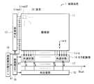
図1は、本開示の一実施の形態に係る撮像装置(撮像装置1)の全体のブロック構成を表すものである。撮像装置1は、例えば後述する放射線等の入射光(撮像光)に基づいて被写体の情報を読み取る(被写体を撮像する)ものである。この撮像装置1は、撮像部11、行走査部13、A/D変換部14、列走査部15、システム制御部16およびバイアス電圧制御部18を備えている。これらのうち、行走査部13、A/D変換部14、列走査部15、システム制御部16およびバイアス電圧制御部18が、本開示における「駆動部」の一具体例に対応し、バイアス電圧制御部18が、本開示における「補正部」の一具体例に対応する。
<Embodiment>
[Overall Configuration of Imaging Device 1]
FIG. 1 illustrates an overall block configuration of an imaging apparatus (imaging apparatus 1) according to an embodiment of the present disclosure. The
(撮像部11)
撮像部11は、入射光(撮像光)に応じて電気信号を発生させるものである。この撮像部11では、画素(撮像画素,単位画素)20が、行列状(マトリクス状)に2次元配置されており、各画素20は、撮像光の光量に応じた電荷量の光電荷を発生して内部に蓄積する光電変換素子(後述の光電変換素子21)を有している。尚、図1中に示したように、以下、撮像部11内における水平方向(行方向)を「H」方向とし、垂直方向(列方向)を「V」方向として説明する。
(Imaging unit 11)
The
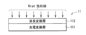
図2は、この撮像部11の概略構成例である。撮像部11は、画素20毎に光電変換素子21が配置された光電変換層111を有している。光電変換層111では、図中に示したように、入射した撮像光Linに基づく光電変換(撮像光Linから信号電荷への変換)がなされるようになっている。
FIG. 2 is a schematic configuration example of the
図3は、画素20の回路構成(いわゆるパッシブ型の回路構成)を、A/D変換部14内の後述する列選択部17の回路構成とともに例示したものである。このパッシブ型の画素20には、1つの光電変換素子21と、1つのトランジスタ22とが設けられている。この画素20にはまた、H方向に沿って延在する読み出し制御線(後述する2つの読み出し制御線Lread1,Lread2)と、V方向に沿って延在する信号線Lsigとが接続されている。
FIG. 3 illustrates a circuit configuration of the pixel 20 (a so-called passive circuit configuration) together with a circuit configuration of a
光電変換素子21は、例えばPIN(Positive Intrinsic Negative)型のフォトダイオードまたはMIS(Metal-Insulator-Semiconductor)型センサからなり、前述したように、入射光(撮像光Lin)の光量に応じた電荷量の信号電荷を発生させるようになっている。尚、この光電変換素子21のカソードは、ここでは蓄積ノードNに接続されている。
The
トランジスタ22は、読み出し制御線(Lread1,Lread2)から供給される行走査信号に応じてオン状態となることにより、光電変換素子21により得られた信号電荷(入力電圧Vin)を信号線Lsigへ出力するトランジスタ(読み出し用トランジスタ)である。このトランジスタ22は、ここではNチャネル型(N型)の電界効果トランジスタ(FET;Field Effect Transistor)により構成されている。但し、トランジスタ22はPチャネル型(P型)のFET等により構成されていてもよい。
The
本実施の形態では、このトランジスタ22が、半導体層(後述の半導体層226)を間にして対向配置された2つのゲート(後述の第1ゲート電極220A,第2ゲート電極220B)を備えた、いわゆるデュアルゲート構造を有している。
In the present embodiment, the
図4は、トランジスタ22の断面構造を表したものである。トランジスタ22は、基板110上に、第1ゲート電極220A(第1のゲート電極)と、この第1ゲート電極220Aを覆うように形成された第1ゲート絶縁膜229を有している。第1ゲート絶縁膜229上には、チャネル層(活性層)226a,LDD(Lightly Doped Drain)層226bおよびN+層226cを含む半導体層226が設けられている。この半導体層226を覆って、第2ゲート絶縁膜230が形成され、第2ゲート絶縁膜230上の第1ゲート電極220Aに対向する領域に、第2ゲート電極220B(第2のゲート電極)が配設されている。第2ゲート電極220B上には、コンタクトホールH1を有する第1層間絶縁膜231が形成されており、このコンタクトホールH1を埋め込むようにソース・ドレイン電極228が形成されている。これらの第1層間絶縁膜231およびソース・ドレイン電極228上には、第2層間絶縁膜232が設けられている。
FIG. 4 illustrates a cross-sectional structure of the
半導体層226は、例えば非晶質シリコン(アモルファスシリコン)、微結晶シリコンまたは多結晶シリコン(ポリシリコン)等のシリコン系半導体、望ましくは低温多結晶シリコン(LTPS:Low Temperature Poly-silicon)により構成されている。あるいは、酸化インジウムガリウム亜鉛(InGaZnO)または酸化亜鉛(ZnO)等の酸化物半導体により構成されていてもよい。この半導体層226では、チャネル層226aとN+層226cとの間に、リーク電流を低減する目的でLDD層226bが形成されている。ソース・ドレイン電極228は、ソースまたはドレインとして機能し、例えばTi、Al、Mo、W、Cr等からなる単層膜またはこれらの積層膜からなる。
The
第1ゲート電極220Aおよび第2ゲート電極220Bはそれぞれ、例えばTi、Al、Mo、W、Cr等のいずれかよりなる単層膜またはそれらの積層膜よりなる。これらの第1ゲート電極220Aおよび第2ゲート電極220Bは、上述のように第1ゲート絶縁膜229、半導体層226および第2ゲート絶縁膜230を挟み込むようにして、互いに対向して設けられている。
Each of the
第1ゲート絶縁膜229および第2ゲート絶縁膜230は、例えば酸化シリコン(SiO2)膜または酸窒化シリコン(SiON)膜等の単層膜であるか、あるいはこのようなシリコン化合物膜と、窒化シリコン(SiNX)膜とを有する積層膜である。例えば、第1ゲート絶縁膜229は、基板110側から順に窒化シリコン膜229Aおよび酸化シリコン膜229Bを積層したものであり、第2ゲート絶縁膜230は、基板110側から順に、酸化シリコン膜230A、窒化シリコン膜230Bおよび酸化シリコン膜230Cを積層したものである。但し、半導体層226が低温多結晶シリコン(低温ポリシリコン)により構成されている場合、第1ゲート絶縁膜229および第2ゲート絶縁膜230では、半導体層226(詳細にはチャネル層226a)と接する面に、酸化シリコン膜(酸化シリコン膜229B,230A)を有することが、製造性の観点から望ましい。
The first
第1層間絶縁膜231および第2層間絶縁膜232は、例えば酸化シリコン膜、酸窒化シリコン膜および窒化シリコン膜のうちの単層膜またはこれらの積層膜により構成されている。例えば、第1層間絶縁膜231は、基板110側から順に酸化シリコン膜231aおよび窒化シリコン膜231bを積層したものであり、第2層間絶縁膜232は、酸化シリコン膜からなる。
The first
本実施の形態では、画素20の回路構成において、例えば第1ゲート電極220Aが読み出し制御線Lread1に接続され、第2ゲート電極220Bが読み出し制御線Lread2に接続されている。このような構成において、第1ゲート電極220Aおよび第2ゲート電極220Bは別々に電圧制御される。具体的には、第1ゲート電極220Aへ印加される電圧は、例えばシステム制御部16および行走査部13により制御され、第2ゲート電極220Bへ印加される電圧は、例えばバイアス電圧制御部18により制御される。これにより、第1ゲート電極220Aには、行走査信号に相当するパルス電圧Vg(第1の電圧)が印加され、第2ゲート電極220Bには、バイアス電圧Vtg(第2の電圧)が印加される。尚、ここでは、パルス電圧が印加される第1ゲート電極220Aを下側(半導体層226よりも下方)に配置し、バイアス電圧が印加される第2ゲート電極220Bを上側(半導体層226よりも上方)に配置しているが、上下逆の構造であってもよい。トランジスタ22のソース(ソース・ドレイン電極228)は、例えば信号線Lsigに接続されており、ドレイン(ソース・ドレイン電極228)は、例えば光電変換素子21のカソードに蓄積ノードNを介して接続されている。また、光電変換素子21のアノードは、ここではグランドに接続(接地)されている。
In the present embodiment, in the circuit configuration of the
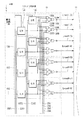
(行走査部13)
行走査部13は、後述のシフトレジスタ回路や所定の論理回路等を含んで構成されており、撮像部11内の複数の画素20に対して行単位(水平ライン単位)での駆動(線順次走査)を行う画素駆動部(行走査回路)である。具体的には、後述する読み出し動作やリセット動作等の撮像動作を例えば線順次走査により行う。尚、この線順次走査は、例えば読み出し制御線Lread1を介して行走査信号を各画素20へ供給することによって行われるようになっている。
(Row scanning unit 13)
The
図5Aは、行走査部13のブロック構成例である。行走査部13は、V方向に沿って延在する複数の単位回路130を有している。尚、ここでは、図中に示した4つの単位回路130に接続された8つの読み出し制御線Lread1を、上から順に、Lread1(1)〜Lread1(8)として示している。
FIG. 5A is a block configuration example of the
各単位回路130は、例えば、1または複数列(ここでは2列)のシフトレジスタ回路131,132(図中のブロック内では便宜上、「S/R」と記載;以下同様)と、4つのAND回路(論理積回路)133A〜133Dと、2つのOR回路(論理和回路)134A,134Bと、2つのバッファ回路135A,135Bとを有している。ここでは、一例として、2列のシフトレジスタ回路を有する構成について説明するが、1列のシフトレジスタ回路により構成されていてもよい。但し、シフトレジスタ回路を2列以上設けることにより、詳述はしないが、1フレーム期間において複数回のリセット動作を行うことができる。
Each
シフトレジスタ回路131は、システム制御部16から供給されるスタートパルスVST1およびクロック信号CLK1に基づいて、複数の単位回路130全体として、V方向に順次シフトするパルス信号を生成する回路である。同様に、シフトレジスタ回路132は、システム制御部16から供給されるスタートパルスVST2およびクロック信号CLK2に基づいて、複数の単位回路130全体として、V方向に順次シフトするパルス信号を生成する回路である。これにより、例えば、シフトレジスタ回路131が、1回目のリセット駆動用のパルス信号を生成し、シフトレジスタ回路132が、2回目のリセット駆動用のパルス信号を生成する。
The
AND回路133A〜133Dにはそれぞれ、シフトレジスタ回路131,132から出力される各パルス信号(各出力信号)の有効期間を制御(規定)するための4種類のイネーブル信号EN1〜EN4が入力されている。具体的には、AND回路133Aでは、一方の入力端子にはシフトレジスタ回路132からのパルス信号が入力され、他方の入力端子にはイネーブル信号EN1が入力されている。AND回路133Bでは、一方の入力端子にはシフトレジスタ回路131からのパルス信号が入力され、他方の入力端子にはイネーブル信号EN2が入力されている。AND回路133Cでは、一方の入力端子にはシフトレジスタ回路132からのパルス信号が入力され、他方の入力端子にはイネーブル信号EN3が入力されている。AND回路133Dでは、一方の入力端子にはシフトレジスタ回路131からのパルス信号が入力され、他方の入力端子にはイネーブル信号EN4が入力されている。
The AND
OR回路134Aは、AND回路133Aからの出力信号とAND回路133Bからの出力信号との論理和信号(OR信号)を生成する回路である。同様に、OR回路134Bは、AND回路133Cからの出力信号とAND回路133Dからの出力信号との論理和信号を生成する回路である。このようにして、上記したAND回路133A〜133DとOR回路134A,134Bとによって、シフトレジスタ回路131,132からの出力信号(パルス信号)同士の論理和信号が、各出力信号の有効期間を制御しつつ生成される。これにより、後述する複数回のリセット駆動の際の駆動タイミング等が規定される。
The OR
バッファ回路135Aは、OR回路134Aからの出力信号(パルス信号)に対するバッファとして機能する回路であり、バッファ回路135Bは、OR回路134Bからの出力信号に対するバッファとして機能する回路である。これらのバッファ回路135A,135Bによるバッファ後のパルス信号(行走査信号)は、読み出し制御線Lread1を介して、撮像部11内の各画素20へ出力される。
The
(A/D変換部14)
A/D変換部14は、複数(ここでは4つ)の信号線Lsigごとに1つ設けられた複数の列選択部17を有しており、信号線Lsigを介して入力した信号電圧(信号電荷)に基づいてA/D変換(アナログ/デジタル変換)を行うものである。これにより、デジタル信号からなる出力データDout(撮像信号)が生成され、外部へ出力されるようになっている。
(A / D converter 14)
The A /
各列選択部17は、例えば図3および図5Bに示したように、チャージアンプ172、容量素子(コンデンサ,フィードバック容量素子)C1、スイッチSW1、サンプルホールド(S/H)回路173、4つのスイッチSW2を含むマルチプレクサ回路(選択回路)174、およびA/Dコンバータ175を有している。これらのうち、チャージアンプ172、容量素子C1、スイッチSW1、S/H回路173およびスイッチSW2はそれぞれ、信号線Lsig毎に設けられている。マルチプレクサ回路174およびA/Dコンバータ175は、列選択部17毎に設けられている。
For example, as shown in FIGS. 3 and 5B, each
チャージアンプ172は、信号線Lsigから読み出された信号電荷を電圧に変換(Q−V変換)するためのアンプ(増幅器)である。このチャージアンプ172では、負側(−側)の入力端子に信号線Lsigの一端が接続され、正側(+側)の入力端子には所定のリセット電圧Vrstが入力されるようになっている。チャージアンプ172の出力端子と負側の入力端子との間は、容量素子C1とスイッチSW1との並列接続回路を介して帰還接続(フィードバック接続)されている。即ち、容量素子C1の一方の端子がチャージアンプ172の負側の入力端子に接続され、他方の端子がチャージアンプ172の出力端子に接続されている。同様に、スイッチSW1の一方の端子がチャージアンプ172の負側の入力端子に接続され、他方の端子がチャージアンプ172の出力端子に接続されている。尚、このスイッチSW1のオン・オフ状態は、システム制御部16からアンプリセット制御線Lcarstを介して供給される制御信号(アンプリセット制御信号)によって制御される。
The
S/H回路173は、チャージアンプ172とマルチプレクサ回路174(スイッチSW2)との間に配置されており、チャージアンプ172からの出力電圧Vcaを一時的に保持するための回路である。
The S /
マルチプレクサ回路174は、列走査部15による走査駆動に従って4つのスイッチSW2のうちの1つが順次オン状態となることにより、各S/H回路173とA/Dコンバータ175との間を選択的に接続または遮断する回路である。
The multiplexer circuit 174 selectively connects each S /
A/Dコンバータ175は、スイッチSW2を介して入力されたS/H回路173からの出力電圧に対してA/D変換を行うことにより、上記した出力データDoutを生成して出力する回路である。
The A /
(列走査部15)
列走査部15は、例えば図示しないシフトレジスタやアドレスデコーダ等を含んで構成されており、上記した列選択部17内の各スイッチSW2を走査しつつ順番に駆動するものである。このような列走査部15による選択走査によって、信号線Lsigの各々を介して読み出された各画素20の信号(上記した出力データDout)が、順番に外部へ出力されるようになっている。
(Column scanning unit 15)
The
(バイアス電圧制御部18)
バイアス電圧制御部18は、例えば上述した第2ゲート電極220Bへ、読み出し制御線Lread2を介してバイアス電圧Vtgを供給すると共に、このバイアス電圧Vtgを、トランジスタ22の閾値電圧Vthのシフト量に応じて補正するものである。このバイアス電圧制御部18によるバイアス電圧Vtgの補正動作は、所定のタイミング、例えば撮像装置起動時に自動的に行われたり、一定期間毎に自動的に行われる。あるいは、外部入力信号(図示しない外部入力手段を介して得られる入力信号)に基づいて手動により行われてもよい。尚、バイアス電圧制御部18の各動作は、システム制御部16からの制御信号に基づいてなされてもよい(図1中の点線矢印A1)が、本実施の形態では、バイアス電圧制御部18が、例えば次のような機能構成を有し、システム制御部16から独立してバイアス電圧制御を行う。
(Bias voltage controller 18)
For example, the bias
図6Aは、バイアス電圧制御部18の機能構成を、読み出し制御線Lread2と共に表したものである。尚、図6Aでは、画素部11に画素行毎に接続される読み出し制御線Lread2のうち、上から3行分の読み出し制御線Lread2(1)〜Lread2(3)を例示している。バイアス電圧制御部18は、例えばFPGA(field-programmable gate array)制御部180と、D/Aコンバータ181と、LDO(Low Drop Out)レギュレータ182とを備える。バイアス電圧制御部18では、FPGA制御部180において、バイアス電圧Vtgの電圧値および切り替えタイミング等が設定される。例えば、図6Bに示したように、バイアス電圧Vtgの電圧値p1,p2,p3,p4と、各電圧値の切り替えタイミングt1,t2,t3が設定される。
FIG. 6A shows the functional configuration of the bias
このようにして設定されたバイアス電圧Vtgは、FPGA制御部18の制御により、D/Aコンバータ181においてデジタル信号からアナログ信号へ変換された後、LDOレギュレータ182を介して出力される。バイアス電圧制御部18から出力されたバイアス電圧Vtgは、読み出し制御線Lread2(1),Lread2(2),Lread2(3),…へそれぞれ供給される。このように、例えばFPGA制御によるバイアス電圧制御部18を用いることで、既存のパネルに外付けでバイアス電圧制御部18を形成可能となり、周辺回路部の設計を大きく変更することなく、後述するような本実施の形態の駆動動作を実現可能となる。
The bias voltage Vtg set in this way is converted from a digital signal to an analog signal by the D /
(システム制御部16)
システム制御部16は、行走査部13、A/D変換部14および列走査部15の各動作を制御するものである。具体的には、システム制御部16は、前述した各種のタイミング信号(制御信号)を生成するタイミングジェネレータを有しており、このタイミングジェネレータにおいて生成される各種のタイミング信号を基に、行走査部13、A/D変換部14および列走査部15の駆動制御を行う。このシステム制御部16の制御に基づいて、行走査部13、A/D変換部14および列走査部15がそれぞれ撮像部11内の複数の画素20に対する撮像駆動(線順次撮像駆動)を行うことにより、撮像部11から出力データDoutが取得されるようになっている。
(System control unit 16)
The
[撮像装置1の作用・効果]
本実施の形態の撮像装置1では、撮像光Linが撮像部11へ入射すると、各画素20内の光電変換素子21では、この撮像光Linが信号電荷に変換(光電変換)される。このとき、蓄積ノードNでは、光電変換により発生した信号電荷の蓄積によって、ノード容量に応じた電圧変化が生じる。具体的には、蓄積ノード容量をCs、発生した信号電荷をqとすると、蓄積ノードNでは(q/Cs)の分だけ電圧が変化(ここでは低下)する。このような電圧変化に応じて、トランジスタ22のドレインには入力電圧Vin(信号電荷に対応した電圧)が供給される。蓄積ノードNに蓄積された信号電荷は、読み出し制御線Lread1から供給される行走査信号に応じてトランジスタ22がオン状態になると、画素20から信号線Lsigへ読み出される。
[Operation and Effect of Imaging Device 1]
In the
読み出された信号電荷は、信号線Lsigを介して複数(ここでは4つ)の画素列ごとに、A/D変換部14内の列選択部17へ入力される。列選択部17では、まず、各信号線Lsigから入力される信号電荷毎に、チャージアンプ172等からなるチャージアンプ回路においてQ−V変換(信号電荷から信号電圧への変換)を行う。次いで、変換された信号電圧(チャージアンプ172からの出力電圧Vca)毎に、S/H回路173およびマルチプレクサ回路174を介してA/Dコンバータ175においてA/D変換を行い、デジタル信号からなる出力データDout(撮像信号)を生成する。このようにして、各列選択部17から出力データDoutが順番に出力され、外部へ伝送される(または図示しない内部メモリーへ入力される)。以下、このような撮像駆動動作について詳細に説明する。
The read signal charges are input to the
(露光期間,読み出し期間における動作)
図7Aおよび図7Bは、露光期間および読み出し期間における画素20および列選択部17内のチャージアンプ回路の動作例を表したものである。尚、以下では説明の便宜上、トランジスタ22のオン・オフ状態を、スイッチを用いて図示している。
(Operation during exposure period and readout period)
FIG. 7A and FIG. 7B show operation examples of the
まず、図7Aに示したように、露光期間Texでは、トランジスタ22はオフ状態となっている。この状態では、画素20内の光電変換素子21へ入射した撮像光Linに基づく信号電荷は、蓄積ノードNに蓄積され、信号線Lsig側へは出力されない(読み出されない)。一方、チャージアンプ回路では、後述するアンプリセット動作(チャージアンプ回路のリセット動作)がなされた後の状態であるため、スイッチSW1がオン状態となっており、結果としてボルテージフォロワ回路が形成されている。
First, as shown in FIG. 7A, in the exposure period Tex, the
続いて、この露光期間Tex後には、画素20から信号電荷を読み出す動作(読み出し動作)と共に、画素20内に蓄積された信号電荷をリセット(排出)するため動作(リセット動作,画素リセット動作)がなされる。本実施の形態では、画素20がパッシブ型の画素回路を有することから、上記読み出し動作に伴ってリセット動作が行われる。以下では、この読み出しおよびリセットが行われる期間を、「読み出し/リセット期間Tr」あるいは単に「期間Tr」と称して説明を行う。
Subsequently, after this exposure period Tex, an operation for reading out signal charges from the pixel 20 (reading operation) and an operation for resetting (discharging) the signal charges accumulated in the pixel 20 (reset operation, pixel reset operation) are performed. Made. In this embodiment, since the
具体的には、読み出し/リセット期間Trでは、図7Bに示したように、トランジスタ22がオン状態となることにより、画素20内の蓄積ノードNから信号線Lsig側へ信号電荷が読み出される(図中の矢印P11参照)。このようにして読み出された信号電荷は、チャージアンプ回路へ入力されるが、この際、チャージアンプ回路では、スイッチSW1がオフ状態となっている(チャージアンプ回路が読み出し動作状態となっている)。従って、チャージアンプ回路へ入力された信号電荷は容量素子C1に蓄積され、その蓄積電荷に応じた信号電圧(出力電圧Vca)がチャージアンプ172から出力される。尚、容量素子C1に蓄積された電荷は、後述するアンプリセット動作の際にスイッチSW1がオン状態となることにより、リセットされる(アンプリセット動作がなされる)。
Specifically, in the read / reset period Tr, as shown in FIG. 7B, the
この読み出し/リセット期間Trでは、上記読み出し動作に伴って、図中の矢印P12で示したように、チャージアンプ回路(チャージアンプ172)の仮想短絡(イマジナリー・ショート)現象を利用したリセット動作がなされる。詳細には、仮想短絡現象によって、チャージアンプ172における負側の入力端子側(信号線Lsig側)の電圧が、正側の入力端子に印加されているリセット電圧Vrstに略等しくなることから、蓄積ノードNもリセット電圧Vrstとなる。このように、パッシブ型の画素回路を用いた本実施の形態では、読み出し/リセット期間Trにおいて、信号電荷の読み出し動作に伴って、蓄積ノードNが所定のリセット電圧Vrstにリセットされる。尚、このような読み出し動作は、各読み出し制御線Lread1に対して線順次になされる。
In the read / reset period Tr, a reset operation using a virtual short-circuit (imaginary short) phenomenon of the charge amplifier circuit (charge amplifier 172) is performed as shown by an arrow P12 in the drawing along with the read operation. The Specifically, the voltage on the negative input terminal side (signal line Lsig side) of the
ここで、図8に、上記のような撮像駆動時の各電圧のタイミング波形を示す。具体的には、読み出し制御線Lread1に供給されるパルス電圧Vg、読み出し制御線Lread2に供給されるバイアス電圧Vtg、チャージアンプ172からの出力電圧Vca、信号線Lsigの電圧Vsig、蓄積ノードNの電圧Vn、の各タイミング波形を表す。尚、各波形では、1ライン分の撮像駆動動作のうちの1フレーム期間ΔTvを含む前後数フレームの期間について示している。
Here, FIG. 8 shows timing waveforms of voltages at the time of image pickup driving as described above. Specifically, the pulse voltage Vg supplied to the read control line Lread1, the bias voltage Vtg supplied to the read control line Lread2, the output voltage Vca from the
1フレーム期間ΔTvでは、まず露光期間Tex(タイミングt11〜t12)において、前述(図7A)のようにして露光動作がなされる。これにより、画素20内の光電変換素子21では、入射した撮像光Linが信号電荷に変換(光電変換)される。この信号電荷が蓄積ノードNに蓄積されることにより、蓄積ノードNの電圧Vnが徐々に変化する(図8中のP31)。ここでは、光電変換素子21のカソード側が蓄積ノードNに接続されているため、露光期間Texでは、電圧Vnがリセット電圧Vrst側から0Vへ向けて徐々に低下する。この露光期間Texでは、トランジスタ22はオフ状態にあるため、読み出し制御線Lread1には、パルス電圧Vgにおけるオン電圧Vonおよびオフ電圧Voffのうち、オフ電圧Voffが印加されている。
In one frame period ΔTv, first, in the exposure period Tex (timing t11 to t12), the exposure operation is performed as described above (FIG. 7A). Thereby, in the
次いで、読み出し/リセット期間Tr(タイミングt12〜t11)において、前述のように、読み出し動作およびリセット動作が行われる。具体的には、読み出し制御線Lread1(即ちトランジスタ22の第1ゲート電極220A)に対し、オン電圧Vonが印加される(オフ電圧Voffからオン電圧Vonへ切り替えられる)。これにより、トラジスタ22がオン状態となる。この後、読み出し制御線Lread1(トランジスタ22の第1ゲート電極220A)に対し、オフ電圧Voffが印加される(オン電圧Vonからオフ電圧Voffへ切り替えられる)ことにより、トラジスタ22がオフ状態となる。尚、オン電圧Vonは、トランジスタ22をオフ状態からオン状態に切り替え可能な電圧であり、パルス電圧Vgにおけるhigh側の電圧(例えば正電位)である。オフ電圧Voffは、トランジスタ22をオン状態からオフ状態に切り替え可能な電圧であり、パルス電圧Vgにおけるlow側の電圧(例えば負電位)である。また、その後、チャージアンプ回路におけるスイッチSW1がオン状態となることにより、このチャージアンプ回路内の容量素子C1に蓄積された電荷がリセットされる(アンプリセット動作が行われる)。
Next, in the read / reset period Tr (timing t12 to t11), the read operation and the reset operation are performed as described above. Specifically, the on voltage Von is applied to the read control line Lread1 (that is, the
一方、上記のような撮像駆動時において、読み出し制御線Lread2(即ち第2ゲート電極220B)には、露光期間Texおよび読み出し/リセット期間Trに亘って一定の電圧(Vtg0)が印加される。この電圧値Vtg0は、例えば撮像装置起動前等に設定されている初期設定の電圧値(あるいはバイアス電圧補正前の電圧値)であり、任意の電圧(例えばグランド)に設定されている。
On the other hand, during the imaging drive as described above, a constant voltage (Vtg0) is applied to the read control line Lread2 (that is, the
このように、本実施の形態では、第1ゲート電極220Aと第2ゲート電極220Bとが別制御され、第1ゲート電極220Aへパルス電圧Vg、第2ゲート電極220Bへバイアス電圧Vtgがそれぞれ印加されることにより、トランジスタ22のオン・オフ制御がなされる。換言すると、パルス電圧Vgがバイアス電圧Vtgによって嵩上げ(または嵩下げ)されて、半導体層226(詳細にはチャネル層226a)に印加され、トランジスタ22のオン・オフ制御がなされる。このようにして、各画素20から、入射した放射線に基づく信号電荷が読み出される。
Thus, in the present embodiment, the
ところで、この撮像装置1へ入射した放射線(X線)の中には、波長変換されずに、撮像部11へ漏れ込むものがあり、このような放射線によりトランジスタ22が被曝すると、次のような不具合が生じる。即ち、トランジスタ22は、第1ゲート絶縁膜129および第2ゲート絶縁膜130に酸化シリコン膜を有するが、この酸素を含む膜中に放射線が入射すると、いわゆる光電効果、コンプトン散乱あるいは電子対生成等により膜中の電子が励起される。その結果、第1ゲート絶縁膜129および第2ゲート絶縁膜130の膜中において、正孔が界面や欠陥にトラップされて溜まり、これに起因して、トランジスタ22の閾値電圧Vthが負側にシフトしてしまう。
By the way, some of the radiation (X-rays) incident on the
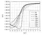
図9に、低温多結晶シリコンを用いたトランジスタ22へX線を照射した場合の、ゲート電圧(Vg)に対するドレイン電流(Id)の関係(電流電圧特性)について示す。このように、放射線を照射した場合、その照射量が、0Gy,54Gy,79Gy,104Gy,129Gy,154Gy,254Gy,354Gyと増大するに従って、閾値電圧Vthが負側にシフトすることがわかる。また、照射量が増すに従って、S(サブスレッショルドスウィング)値も悪化している。加えて、この閾値電圧Vthのシフト量の増加は、オフ電流およびオン電流の変化を引き起こす。例えば、オフ電流が増して電流リークが生じたり、オン電流が減少して読み出し不能になる等、トランジスタの信頼性を維持することが困難となる。このように、特に低温多結晶ポリシリコンを用いた放射線撮像装置では、被曝によってトランジスタ22の閾値電圧Vthが負側へシフトし、これが信頼性低下の要因となっている。そこで、本実施の形態では、以下のような閾値電圧Vthのシフト量を考慮した補正(キャリブレーション)がなされる。
FIG. 9 shows the relationship (current-voltage characteristics) of the drain current (Id) with respect to the gate voltage (Vg) when the
(バイアス電圧補正動作)
バイアス電圧制御部18は、例えば上述したFPGA制御により、所定のタイミングで、上記のようなバイアス電圧Vtgを、トランジスタ22の閾値電圧Vthのシフト量に応じて補正する。具体的には、以下のようにして補正を行う。
(Bias voltage correction operation)
The bias
図10は、バイアス電圧Vtgの補正時の駆動動作について説明するもので、各電圧のタイミング波形を表している。タイミング波形としては、上記撮像駆動時と同様、パルス電圧Vg、バイアス電圧Vtg、出力電圧Vca、電圧Vsigおよび電圧Vnについて示している。 FIG. 10 explains the driving operation at the time of correcting the bias voltage Vtg, and shows the timing waveform of each voltage. As timing waveforms, the pulse voltage Vg, the bias voltage Vtg, the output voltage Vca, the voltage Vsig, and the voltage Vn are shown as in the case of the imaging drive.
まず、バイアス電圧制御部18は、暗状態(非露光状態)において、読み出し制御線Lread2に対して供給する電圧の値を変化させて、その電圧値毎の信号出力(例えば画素値)をサンプリングする。例えば、バイアス電圧Vtgにおいて、電圧値を一定間隔で(期間Ta毎に)電圧Vtg(1),Vtg(2),Vtg(3),…と段階的に変化させつつ、上述したような撮像駆動時と同様の読み出し動作を行う。期間Taは、任意に設定されればよいが、例えば1フレーム期間以上の期間に設定される。また、数フレーム期間に亘って期間Taが設定されてもよく、その場合には、各フレームの平均値を、そのフレームに印加された電圧値に対応する画素値としてもよい。例えば、期間Taを2フレーム期間(2ΔTv)として、電圧Vtg(1)(Vtg(2),Vtg(3)についても同様)を印加しつつフレーム毎に画素値b1,b2を取得し、その2つの画素値b1,b2の平均値b12を、電圧Vtg(1)(あるいはVtg(2),Vtg(3))に対応する画素値としてもよい。図10では、一例として、Vtg(1)=−0.5V、Vtg(2)=0V,Vtg(3)=0.5V,…のように、バイアス電圧Vtgの電圧値を例えば0.5V刻みで変化させている。
First, the bias
図11は、バイアス電圧Vtgがグランド(0V)に設定された状態において、X線未照射の場合(線量0Gy)の電流電圧特性(電流電圧特性A)と、X線を照射した場合(管電圧80kV,線量75Gy)の電流電圧特性(電流電圧特性B)を表したものである。このように、X線の照射によって電流電圧特性が変化し、これに伴って閾値電圧Vthも負側に大きくシフトする。このX線照射後の電流電圧特性Bを有するトランジスタ22に対し、バイアス電圧Vtgの値を、−3V〜3Vの範囲において1.0V刻みで変化させた各場合の電流電圧特性について、図12に示す。尚、ドレインおよびソース間の電圧Vdsは0.1Vとした。
FIG. 11 shows the current-voltage characteristics (current-voltage characteristics A) when X-rays are not irradiated (
図12に示したように、X線照射後のトランジスタ22に対して印加するバイアス電圧Vtgの値を変化させると、電流電圧特性Bが正方向または負方向へ平行シフトしていることがわかる。つまり、バイアス電圧Vtgを変化させることで、トランジスタ22の閾値電圧Vthのシフト分を補填することができ、閾値電圧Vthシフトに追従したオン・オフ制御を行うことが可能となる。
As shown in FIG. 12, when the value of the bias voltage Vtg applied to the
具体的には、以下のようにして、閾値電圧Vthのシフト量に応じたバイアス電圧Vtgの最適電圧値(電圧値Vtg1)を求め、その後の撮像駆動動作において使用するバイアス電圧Vtgを、電圧値Vtg0から電圧値Vtg1へ変更する。まず、バイアス電圧制御部18では、初期状態(X線照射量0Gy)でのバイアス電圧Vtgの閾値電圧(V0とする)を予め保持しておく。この初期状態における閾値電圧V0と、補正時におけるバイアス電圧Vtgの閾値電圧(V1とする)との比較から、トランジスタ22の閾値電圧Vthのシフト量に応じたバイアス電圧Vtgの値を決定する。
Specifically, as described below, an optimum voltage value (voltage value Vtg1) of the bias voltage Vtg corresponding to the shift amount of the threshold voltage Vth is obtained, and the bias voltage Vtg used in the subsequent imaging driving operation is determined as the voltage value. The voltage value is changed from Vtg0 to the voltage value Vtg1. First, the bias
例えば、図13に示したように、撮像装置1の初期設定として、図10において説明した駆動動作と同様の動作を行い、初期状態における、バイアス電圧Vtgの電圧値Vtg(1),Vtg(2),Vtg(3),…毎の画素値を予めサンプリングし、保持しておく。これらの電圧値毎の画素値から、画素値の基準値に対応するバイアス電圧Vtgの値を求め、これを、初期状態におけるバイアス電圧Vtgの基準電圧V0とする。補正時には、図10において説明した駆動動作を行い、上述したように、バイアス電圧Vtgの電圧値Vtg(1),Vtg(2),Vtg(3),…毎の画素値をサンプリングする。図13には、その一例として、75Gy照射後にサンプリングした画素値をプロットしている。但し、ここでは、画素値の基準値を例えば1000LSBとして、基準電圧V0(例えば4.6V)を設定している。この画素値は、LSB(Least Significant Bit)に対応するものであり、例えば以下の式(1)によって表される。
For example, as shown in FIG. 13, as the initial setting of the
画素値(LSB)=トランジスタ22のリーク電流(A)/フレームレート(fps)/素電荷(C)/158LSB+光電変換素子21のリーク定数A ……(1)
Pixel value (LSB) = leakage current (A) of
ここでは、フレームレート7.5(fps)、1LSB=158e-、素電荷1.602×E-19(C)、定数A=0として算出している。尚、パルス電圧Vgにおけるオフ電圧は−4Vとした。また、1LSBの上記値は一例であり、これはアンプICによって異なるものである。 Here, the frame rate is 7.5 (fps), 1LSB = 158e − , elementary charge 1.602 × E −19 (C), and constant A = 0. The off voltage in the pulse voltage Vg was set to -4V. Further, the above value of 1LSB is an example, and this differs depending on the amplifier IC.
この後、補正時においてサンプリングした電圧値毎の画素値に基づいて、バイアス電圧Vtgの基準電圧V1(画素値100LSBに対応するバイアス電圧Vtg)を算出する。このようにして算出した基準電圧V1と、初期状態の基準電圧V0とを比較し、基準電圧V1の基準電圧V0からのシフト量を算出する。このシフト量を初期設定の電圧値Vtg0に加算する(式(2))。例えば、初期設定の電圧値Vtg0が0V,基準電圧V0が4.6V、補正時の基準電圧V1が3.0Vである場合には、式(3)に示したように、電圧値Vtg1を−1.6Vに設定すればよい。即ち、この例では、バイアス電圧Vtgの電圧値を、Vtg0(0V)からVtg1(−1.6V)に変更する補正がなされる。
Vtg1=Vtg0+(V1−V0) ……(2)
Vtg1=0V+(3.0V−4.6V)=−1.6V ……(3)
Thereafter, the reference voltage V1 of the bias voltage Vtg (the bias voltage Vtg corresponding to the pixel value 100LSB) is calculated based on the pixel value for each voltage value sampled at the time of correction. The reference voltage V1 calculated in this way is compared with the reference voltage V0 in the initial state, and the shift amount of the reference voltage V1 from the reference voltage V0 is calculated. This shift amount is added to the initially set voltage value Vtg0 (formula (2)). For example, when the initial voltage value Vtg0 is 0 V, the reference voltage V0 is 4.6 V, and the reference voltage V1 at the time of correction is 3.0 V, the voltage value Vtg1 is − What is necessary is just to set to 1.6V. That is, in this example, correction is performed to change the voltage value of the bias voltage Vtg from Vtg0 (0V) to Vtg1 (−1.6V).
Vtg1 = Vtg0 + (V1-V0) (2)
Vtg1 = 0V + (3.0V-4.6V) =-1.6V (3)
上記のように、本実施の形態では、所定のタイミングにおいて、バイアス電圧制御部18が、バイアス電圧Vtgの電圧値毎に画素値のサンプリングを行い、サンプリングした画素値に基づいて、トランジスタ22の閾値電圧Vthのシフト分を補填し得る、バイアス電圧Vtgの最適値(電圧値Vtg1)を算出する。バイアス電圧制御部18は、算出した電圧値Vtg1を、所定のタイミングで読み出し制御線Lread2へ出力する。補正後は、バイアス電圧Vtgとして電圧値Vtg1が読み出し制御線Lread2(第2ゲート電極220B)に印加されつつ、トランジスタ22のオン・オフ制御がなされる。尚、バイアス電圧補正のタイミングは任意であり、1度補正した後に、所定の間隔をあけて再度補正を行ってもよい。このように複数回にわたって補正を行う場合には、上述したような一連の補正動作がその都度行われる。
As described above, in the present embodiment, at a predetermined timing, the bias
尚、バイアス電圧補正に用いるパラメータとしては、上述したような暗状態の画素値に限らず、例えば明状態(露光状態)と暗状態との間の画素値の変化量であってもよい。この場合、初期状態において、電圧Vtg(1),Vtg(2),Vtg(3),…の電圧値毎に、明状態と暗状態との各状態における画素値を求め、各状態間の画素値の変化量をサンプリングすればよい。 The parameter used for bias voltage correction is not limited to the pixel value in the dark state as described above, but may be a change amount of the pixel value between the bright state (exposure state) and the dark state, for example. In this case, in the initial state, for each voltage value of voltages Vtg (1), Vtg (2), Vtg (3),... What is necessary is just to sample the amount of change of a value.
以上のように本実施の形態では、各画素20からの信号電荷の読み出しの際、トランジスタ22の第1ゲート電極220Aにパルス電圧Vgを、第2ゲート電極220Bにバイアス電圧Vtgがそれぞれ印加され、トランジスタのオン・オフ制御がなされる。このとき、所定のタイミングにおいて、バイアス電圧制御部18が、バイアス電圧Vtgを、トランジスタ22の閾値電圧Vthのシフト量に応じて補正する。これにより、トランジスタの閾値電圧のシフトによる影響を緩和して高信頼性を実現することが可能となる。
As described above, in the present embodiment, when the signal charge is read from each
続いて、上記実施の形態の変形例(変形例1〜8)について説明する。尚、上記実施の形態における構成要素と同一のものには同一の符号を付し、適宜説明を省略する。 Subsequently, modified examples (modified examples 1 to 8) of the above-described embodiment will be described. In addition, the same code | symbol is attached | subjected to the same thing as the component in the said embodiment, and description is abbreviate | omitted suitably.
<変形例1>
上記実施の形態では、撮像駆動動作の際に、読み出し制御線Lread2(第2ゲート電極220B)に印加されるバイアス電圧Vtgの電圧値は、補正動作によって電圧値が切り替えられるタイミングまでの期間は一定である。ところが、第2ゲート電極220Bが、固定の電位を有すると、この第2ゲート電極220Bと半導体層226(詳細にはチャネル層226a)との間に、寄生容量が生じる。これによって、読み出し制御線Lread1(第1ゲート電極220A)に印加されるパルス電圧Vgに対するスイッチング動作(トランジスタ22のオンおよびオフの切り替え動作)の応答が遅くなることがある。
<
In the above embodiment, the voltage value of the bias voltage Vtg applied to the read control line Lread2 (
そこで、本変形例では、読み出し制御線Lread1にパルス電圧Vgにおけるオン電圧Vonが印加されている期間(例えば図8の期間Tr)、読み出し制御線Lread2(第2ゲート電極220B)をいわゆるフローティング状態に保持する駆動がなされる。
Therefore, in this modification, the read control line Lread2 (
図14は、本変形例の接点構成例をバイアス電圧制御部18およびシステム制御部16と共に表したものである。このように、本変形例では、読み出し制御線Lread2とバイアス電圧制御部18(電圧補正線L1)との間にスイッチ(SW11)を有している。スイッチSW11のオン状態およびオフ状態の切り替えは、図示しない制御信号(例えば行走査部からの制御信号)によってなされる。
FIG. 14 illustrates a contact configuration example of this modification together with the bias
本変形例では、上記構成により、読み出し制御線Lread1へのオン電圧Vonの印加タイミングに同期して、スイッチSW11がオフ状態(開状態)に制御される。これにより、第2ゲート電極220Bがフローティング状態となり、読み出し/リセット期間Tr中において、上述のような寄生容量の発生が抑制される。一方、このような読み出し/リセット期間Tr以外の期間(即ちトランジスタ22のオフ期間)には、スイッチSW11がオン状態(閉状態)に制御され、上記実施の形態と同様の駆動動作がなされる。このように、オフ期間中には、閾値電圧のシフト量に応じて設定されたバイアス電圧Vtgを印加することにより、閾値電圧シフトに起因するオフリーク増大等を抑制できる。よって、読み出し時の寄生容量の発生を抑制しつつ、上記実施の形態と同等の効果を得ることができる。
In the present modification, with the above configuration, the switch SW11 is controlled to be in the off state (open state) in synchronization with the application timing of the on voltage Von to the read control line Lread1. As a result, the
<変形例2>
上記変形例1では、読み出し制御線Lread1へのオン電圧Vonの印加期間中、読み出し制御線Lread2をフローティング状態に切り替えたが、本変形例のように、読み出し制御線Lread2にオン電圧Vonと同値の電圧を印加してもよい。即ち、読み出し/リセット期間Tr中は、読み出し制御線Lread1,Lread2を同電位に保持するようにしてもよい。
<
In the first modification, the read control line Lread2 is switched to the floating state during the application period of the on voltage Von to the read control line Lread1, but the read control line Lread2 has the same value as the on voltage Von as in this modification. A voltage may be applied. That is, the read control lines Lread1 and Lread2 may be held at the same potential during the read / reset period Tr.
図15は、本変形例のバイアス電圧制御部18Aの機能構成をシステム制御部16と共に表したものである。このように、本変形例では、バイアス電圧制御部18Aが、読み出し制御線Lread2にいわゆる共通接点cを有するスイッチ(スイッチSW12)が設けられている。このスイッチSW12は、共通接点cと、2つの接点a,bを有する切り替えスイッチであり、これにより、バイアス電圧制御部18Aから2値の電圧値を択一的に出力できるようになっている。例えば、バイアス電圧制御部18Aは、バイアス電圧Vtgの電圧値を生成する回路部18a1と、読み出し/リセット期間中に印加する電圧値を生成する回路部18a2とを有しており、これらの回路部18a1,18a2はFPGA制御部180によって制御される。回路部18a1はスイッチSW12の接点aに、回路部18a2はスイッチSW12の接点bに、それぞれ接続されている。尚、スイッチSW12の切り替えは、図示しない制御信号によってなされ、例えば、通常時(スイッチSW12のオフ時)は接点aにつながり、動作時(スイッチSW12のオン時)には接点bにつながるようになっている。
FIG. 15 illustrates a functional configuration of the bias
本変形例では、上記構成により、読み出し制御線Lread1へのオン電圧Vonの印加タイミングに同期して、読み出し制御線Lread2が、スイッチSW12の接点bを介して回路部18a2へ接続される。これにより、読み出し制御線Lread2へオン電圧Vonが印加され、読み出し制御線Lread1,Lread2が同電位となる。これにより、読み出し/リセット期間Tr中において、上述のような寄生容量の発生を抑制できる。一方、このような読み出し/リセット期間Tr以外の期間(即ちトランジスタ22のオフ期間)には、読み出し制御線Lread2が、接点aを介して回路部18a1へ接続され、上記実施の形態と同様の駆動動作がなされる。よって、本変形例によいても、上記実施の形態および変形例1と同等の効果を得ることができる。
In the present modification, the read control line Lread2 is connected to the circuit unit 18a2 via the contact b of the switch SW12 in synchronization with the application timing of the ON voltage Von to the read control line Lread1. As a result, the ON voltage Von is applied to the read control line Lread2, and the read control lines Lread1 and Lread2 have the same potential. Thereby, the generation of the parasitic capacitance as described above can be suppressed during the read / reset period Tr. On the other hand, in a period other than the read / reset period Tr (that is, the off-period of the transistor 22), the read control line Lread2 is connected to the circuit unit 18a1 through the contact a, and is driven in the same manner as in the above embodiment. Action is taken. Therefore, even if it is suitable for this modification, the same effect as the above-mentioned embodiment and
<変形例3>
図16は、変形例3に係る画素(画素20A)の回路構成を、上記実施の形態で説明した列選択部17の回路構成例と共に表したものである。本変形例の画素20Aは、実施の形態の画素20と同様にいわゆるパッシブ型の回路構成となっており、1つの光電変換素子21と1つのトランジスタ22とを有している。また、この画素20AにはH方向に沿って延在する読み出し制御線Lread1,Lread2と、V方向に沿って延在する信号線Lsigとが接続されている。
<
FIG. 16 illustrates a circuit configuration of a pixel (pixel 20A) according to
但し、本変形例の画素20Aでは、上記実施の形態の画素20とは異なり、光電変換素子21のアノードが蓄積ノードNに接続され、カソードがグランド(接地)に接続されている。このように、画素20Aにおいて光電変換素子21のアノードに蓄積ノードNが接続されるようにしてもよく、このように構成した場合であっても、上記実施の形態の撮像装置1と同様の効果を得ることが可能である。
However, in the pixel 20A of this modification, unlike the
<変形例4>
図17は、変形例4に係る画素(画素20B)の回路構成を、上記実施の形態で説明した列選択部17の回路構成例と共に表したものである。本変形例の画素20Bは、実施の形態の画素20と同様にいわゆるパッシブ型の回路構成となっており、1つの光電変換素子21を有しており、H方向に沿って延在する読み出し制御線Lread1,Lread2と、V方向に沿って延在する信号線Lsigとに接続されている。
<
FIG. 17 illustrates a circuit configuration of a pixel (pixel 20B) according to
但し、本変形例では、画素20Bが、2つのトランジスタ22(トランジスタ22B1,22B2)を有している。これら2つのトランジスタ22B1,22B2は、互いに直列に接続されている(一方のソースまたはドレインと他方のソースまたはドレインとが電気的に接続されている。または、後述するように半導体層226が一体的に連結して形成されている。)。また、各トランジスタ22B1,22B2における一方のゲートが読み出し制御線Lread1に接続され、他方のゲートが読み出し制御線Lread2に接続されている。
However, in this modification, the pixel 20B includes two transistors 22 (transistors 22B1 and 22B2). These two transistors 22B1 and 22B2 are connected in series with each other (one source or drain and the other source or drain are electrically connected. Alternatively, as described later, a
図18に、このような2つのトランジスタ22B1,22B2の断面構成例を示す。図18に示したように、2つのゲート電極220A,220Bにより半導体層226を挟み込んだ積層構造が2つ並んで形成されており、これらの積層構造の両側に一対のソース・ドレイン電極228が配設されている。尚、この例では、トランジスタ22B1,22B2において、半導体層226が一体化されている。具体的には、基板110上の選択的な領域に、2つの第1ゲート電極220Aを有し、これらの第1ゲート電極220Aを覆うように第1ゲート絶縁膜229および半導体層226が設けられている。この半導体層226上には、第2ゲート絶縁膜230が形成され、第2ゲート絶縁膜230上の選択的な領域(2つの第1ゲート電極220Aのそれぞれに対向する領域)に、第2ゲート電極220Bが配設されている。これらの第2ゲート電極220Bを覆って第1層間絶縁膜231が形成されており、この第1層間絶縁膜231上には、コンタクトホールH1を埋め込むように一対のソース・ドレイン電極228が配設されている。ソース・ドレイン電極228上には、2つのトランジスタ22B1,22B2を覆うように、第2層間絶縁膜232が設けられている。尚、本変形例のように、ゲート電極を並設させることにより、オフリークを低減させることができる。
FIG. 18 shows a cross-sectional configuration example of such two transistors 22B1 and 22B2. As shown in FIG. 18, two stacked structures in which the
このように、画素20B内に直列接続させた2つのトランジスタ22B1,22B2を設けてもよく、この場合にも、上記実施の形態で説明したような撮像駆動動作および補正動作を行うことにより、閾値電圧Vthのシフトによる影響を軽減することができる。尚、3つ以上のトランジスタを直列接続させてもよい。 As described above, two transistors 22B1 and 22B2 connected in series may be provided in the pixel 20B. In this case, the threshold value is obtained by performing the imaging driving operation and the correction operation as described in the above embodiment. The influence due to the shift of the voltage Vth can be reduced. Three or more transistors may be connected in series.
<変形例5,6>
図19は、変形例5に係る画素(画素20C)の回路構成を、以下説明する列選択部17Bの回路構成例とともに表したものである。また、図20は、変形例6に係る画素(画素20D)の回路構成を、列選択部17Bの回路構成例とともに表したものである。これらの変形例5,6に係る画素20C,20Dはそれぞれ、これまで説明した画素20,20A,20Bとは異なり、いわゆるアクティブ型の画素回路を有している。
<
FIG. 19 illustrates a circuit configuration of a pixel (pixel 20C) according to
このアクティブ型の画素20C,20Dには、1つの光電変換素子21と、3つのトランジスタ22,23,24とが設けられている。これらの画素20C,20Dにはまた、H方向に沿って延在する読み出し制御線Lread1,Lread2およびリセット制御線Lrstと、V方向に沿って延在する信号線Lsigとが接続されている。
The active pixels 20C and 20D are provided with one
画素20C,20Dではそれぞれ、トランジスタ22の一方のゲートが読み出し制御線Lread1、他方のゲートが読み出し制御線Lread2にそれぞれ接続され、ソースが信号線Lsigに接続され、ドレインが、ソースフォロワ回路を構成するトランジスタ23のドレインに接続されている。トランジスタ23のソースは電源VDDに接続され、ゲートは、蓄積ノードNを介して、光電変換素子21のカソード(図19の例)またはアノード(図20の例)と、リセット用トランジスタとして機能するトランジスタ24のドレインとに接続されている。トランジスタ24のゲートはリセット制御線Lrstに接続され、ソースにはリセット電圧Vrstが印加されるようになっている。図19の変形例5では、光電変換素子21のアノードがグランドに接続され、図20の変形例6では、光電変換素子21のカソードがグランドに接続されている。尚、簡便化のため、図20では、トランジスタ23,24のゲートを1つのみ図示しているが、詳細には、トランジスタ23,24は、トランジスタ22と同様の2つのゲート電極を有する素子構造を有する。トランジスタ23,24では、例えば2つのゲート電極がショートした状態で駆動されるため、1つのゲートを有する素子構造のものと回路的には等価となる。但し、3つのトランジスタ22,23,24のうち少なくともトランジスタ22が上述したような2つのゲート電極を有するものであれば、本開示の効果を得ることができる。
In each of the pixels 20C and 20D, one gate of the
また、これらの変形例5,6において列選択部17Bは、前述した列選択部17において、チャージアンプ172、容量素子C1およびスイッチSW1に代わりに、定電流源171およびアンプ176を設けたものとなっている。アンプ176では、正側の入力端子には信号線Lsigが接続されると共に、負側の入力端子と出力端子とが互いに接続され、ボルテージフォロワ回路が形成されている。尚、信号線Lsigの一端側には定電流源171の一方の端子が接続され、この定電流源171の他方の端子には電源VSSが接続されている。
In these modification examples 5 and 6 , the column selection unit 17B includes a constant
<変形例7,8>
図21Aおよび図21Bはそれぞれ、変形例7,8に係る撮像部11の概略構成を模式的に表したものである。上記実施の形態の撮像装置1が、放射線撮像装置である場合には、撮像部11は、これらの変形例7,8のいずれかの構成を有している。
<
21A and 21B schematically show the schematic configuration of the
図21Aに示した変形例7に係る撮像部11は、いわゆる間接変換型の放射線撮像装置に適用されるものであり、光電変換層111上(受光面側)に、波長変換層112を有している。波長変換層112は、放射線Rrad(α線,β線,γ線,X線等)を、光電変換層111の感度域の波長に波長変換するものであり、これにより光電変換層111では、この放射線Rradに基づく情報を読み取ることが可能となる。この波長変換層112は、例えばX線などの放射線を可視光に変換する蛍光体(例えば、シンチレータ)からなる。このような波長変換層112は、例えば有機平坦化膜、スピンオングラス材料等からなる平坦化膜、および蛍光体膜をこの順に積層したものである。蛍光体膜は、例えばCsI(Tl添加),Gd2O2S,BaFX(XはCl,Br,I等),NaIまたはCaF2等からなる。
The
図21Bに示した変形例8に係る撮像部11は、いわゆる直接変換型の放射線撮像装置に適用されるものであり、入射した放射線Rradを吸収して電気信号に変換する光電変換層111を有している。本変形例の光電変換層111は、例えば、アモルファスセレン(a−Se)半導体や、カドミニウムテルル(CdTe)半導体などにより構成されている。尚、この直接変換型の場合の画素20の回路構成は、図3に示した各要素のうち光電変換素子21を容量に置き換えたものとなる。
The
上記のような間接変換型または直接変換型の放射線撮像装置は、入射した放射線Rradに基づいて電気信号を得る、様々な種類の撮像装置として利用される。例えば、医療用のX線撮像装置(Digital Radiography等)、空港等で用いられる携帯物検査用X線撮影装置、工業用X線撮像装置(例えば、コンテナ内の危険物等の検査を行う装置)などに適用可能である。 The indirect conversion type or direct conversion type radiation imaging apparatus as described above is used as various types of imaging apparatuses that obtain an electrical signal based on incident radiation Rrad. For example, medical X-ray imaging devices (Digital Radiography, etc.), portable object inspection X-ray imaging devices used in airports, etc., industrial X-ray imaging devices (for example, devices for inspecting dangerous materials in containers) It is applicable to.
<適用例>
続いて、上記実施の形態および変形例(変形例1〜8)に係る撮像装置は、以下に説明するような撮像表示システムへ適用することも可能である。
<Application example>
Subsequently, the imaging apparatus according to the above-described embodiment and modifications (
図22は、適用例に係る撮像表示システム(撮像表示システム5)の概略構成例を模式的に表したものである。撮像表示システム5は、上記実施の形態等に係る撮像部11等を有する撮像装置1と、画像処理部52と、表示装置4とを備えており、この例では放射線を用いた撮像表示システム(放射線撮像表示システム)となっている。
FIG. 22 schematically illustrates a schematic configuration example of an imaging display system (imaging display system 5) according to an application example. The
画像処理部52は、撮像装置1から出力される出力データDout(撮像信号)に対して所定の画像処理を施すことにより、画像データD1を生成するものである。表示装置4は、画像処理部52において生成された画像データD1に基づく画像表示を、所定のモニタ画面40上で行うものである。
The
この撮像表示システム5では、撮像装置1(ここでは放射線撮像装置)が、光源(ここではX線源等の放射線源)51から被写体50に向けて照射された照射光(ここでは放射線)に基づき、被写体50の画像データDoutを取得し、画像処理部52へ出力する。画像処理部52は、入力された画像データDoutに対して上記した所定の画像処理を施し、その画像処理後の画像データ(表示データ)D1を表示装置4へ出力する。表示装置4は、入力された画像データD1に基づいて、モニタ画面40上に画像情報(撮像画像)を表示する。
In this
このように、本適用例の撮像表示システム5では、撮像装置1において被写体50の画像を電気信号として取得可能であるため、取得した電気信号を表示装置4へ伝送することによって画像表示を行うことができる。即ち、従来のような放射線写真フィルムを用いることなく、被写体50の画像を観察することが可能となり、また、動画撮影および動画表示にも対応することが可能となる。
As described above, in the
尚、本適用例では、撮像装置1が放射線撮像装置として構成されており、放射線を用いた撮像表示システムとなっている場合を例に挙げて説明したが、本開示の撮像表示システムは、他の方式の撮像装置を用いたものにも適用することが可能である。
In this application example, the case where the
以上、実施の形態、変形例および適用例を挙げたが、本開示内容はこれらの実施の形態等に限定されず、種々の変形が可能である。例えば、上記実施の形態等では、トランジスタ22において、半導体層226よりも下方に第1ゲート電極220Aが配置され、上方に第2ゲート電極220Bが配置された構成を例に挙げたが、これらが上下逆の構成となっていてもよい。即ち、2つのゲート電極のうちの上下どちらの電極に、パルス電圧(あるいはバイアス電圧)を印加してもよい。
As mentioned above, although embodiment, the modification, and the application example were mentioned, this indication content is not limited to these embodiment etc., A various deformation | transformation is possible. For example, in the above-described embodiment and the like, the
また、上記実施の形態等では、第1ゲート電極220Aに印加されるパルス電圧と、第2ゲート電極220Bに印加されるバイアス電圧とのうち、バイアス電圧の電圧値を補正する場合について説明したが、補正される電圧値はこれに限定されない。即ち、パルス電圧の電圧値のみが補正されてもよいし、パルス電圧とバイアス電圧との両方が補正されてもよい。但し、上記実施の形態等において説明したように、バイアス電圧を補正する場合の方が、行走査部13等の回路構成を複雑化させずに済むので望ましい。
In the above-described embodiment and the like, the case where the voltage value of the bias voltage is corrected among the pulse voltage applied to the
更に、上記実施の形態等では、トランジスタ22の2つのゲート電極のうち一方のゲート電極(第1ゲート電極220A)にパルス電圧、他方のゲート電極(第2ゲート電極220B)にバイアス電圧をそれぞれ印加するようにしたが、各ゲート電極に印加される電圧は、これらに限定されるものではない。
Further, in the above-described embodiment, a pulse voltage is applied to one of the two gate electrodes of the transistor 22 (
加えて、上記実施の形態等の撮像部における画素の回路構成は、上記実施の形態等で説明したもの(画素20,20A〜20Dの回路構成)には限られず、他の回路構成であってもよい。同様に、行走査部や列選択部等の回路構成についても、上記実施の形態等で説明したものには限られず、他の回路構成であってもよい。
In addition, the circuit configuration of the pixels in the imaging unit of the above-described embodiment and the like is not limited to the one described in the above-described embodiments (circuit configuration of the
また、上記実施の形態等で説明した撮像部、行走査部、A/D変換部(列選択部)および列走査部等はそれぞれ、例えば同一基板上に形成されているようにしてもよい。具体的には、例えば低温多結晶シリコンなどの多結晶半導体を用いることにより、これらの回路部分におけるスイッチ等も同一基板上に形成することができるようになる。このため、例えば外部のシステム制御部からの制御信号に基づいて、同一基板上における駆動動作を行うことが可能となり、狭額縁化(3辺フリーの額縁構造)や配線接続の際の信頼性向上を実現することができる。 Further, the imaging unit, the row scanning unit, the A / D conversion unit (column selection unit), the column scanning unit, and the like described in the above embodiments may be formed on the same substrate, for example. Specifically, by using a polycrystalline semiconductor such as low-temperature polycrystalline silicon, switches and the like in these circuit portions can be formed on the same substrate. For this reason, for example, it becomes possible to perform a driving operation on the same substrate based on a control signal from an external system control unit, and to improve reliability when narrowing the frame (three-side free frame structure) or wiring connection. Can be realized.
尚、本開示は以下のような構成を取ることも可能である。
(1)
各々が光電変換素子と電界効果型のトランジスタとを含む複数の画素を有する撮像部と、
前記トランジスタを電圧制御して、前記画素内に蓄積された信号電荷の読み出し駆動を行う駆動部と、
前記トランジスタを駆動するための電圧値を補正する補正部と
を備え、
前記トランジスタは、半導体層を間にして対向配置された第1および第2のゲート電極を有し、
前記駆動部は、前記トランジスタの前記第1のゲート電極に第1の電圧を印加すると共に、前記第2のゲート電極に第2の電圧を印加することにより、前記トランジスタのオン・オフ制御を行い、
前記補正部は、前記閾値電圧のシフト量に応じて前記第1および第2の電圧のうちの少なくとも一方の電圧値を補正する
撮像装置。
(2)
前記第1の電圧はパルス電圧であり、前記第2の電圧はバイアス電圧である
上記(1)に記載の撮像装置。
(3)
前記補正部は、所定のタイミングで、前記閾値電圧のシフト量に応じて前記第2の電圧の電圧値を補正する
上記(2)に記載の撮像装置。
(4)
前記撮像部は、入射した放射線に基づいて電気信号を発生させるものである
上記(1)〜(3)のいずれかに記載の撮像装置。
(5)
前記トランジスタは、シリコン酸化物膜を含むゲート絶縁膜を有する
上記(1)〜(4)のいずれかに記載の撮像装置。
(6)
前記半導体層は、多結晶シリコン、微結晶シリコン、非結晶シリコンまたは酸化物半導体を含む
上記(1)〜(5)のいずれかに記載の撮像装置。
(7)
前記半導体層は、低温多結晶シリコンを含む
上記(6)に記載の撮像装置。
(8)
前記補正部は、
非露光状態において、前記第2の電圧として複数の電圧値を段階的に変化させて印加しつつ、前記複数の電圧値のそれぞれに対応する画素値をサンプリングし、
サンプリングした複数の画素値に基づいて、前記閾値電圧のシフト量に応じた前記第2の電圧の最適値を算出する
上記(3)に記載の撮像装置。
(9)
前記駆動部は、前記第1の電圧におけるオン電圧の印加期間中、前記第2のゲート電極をフローティング状態に保持する
上記(2),(3),(8)のいずれかに記載の撮像装置。
(10)
前記駆動部は、前記第1の電圧におけるオン電圧の印加期間中、前記第2のゲート電極に対し、前記オン電圧と同値の電圧を印加する
上記(2),(3),(8)のいずれかに記載の撮像装置。
(11)
前記撮像部は、前記光電変換素子の光入射側に、前記放射線を前記光電変換素子の感度域の波長に変換する波長変換層を有する
上記(4)に記載の撮像装置。
(12)
前記複数の画素はそれぞれ、前記放射線を吸収して電気信号に変換するものである
上記(4)に記載の撮像装置。
(13)
前記放射線はX線である
上記(4),(11),(12)に記載の撮像装置。
(14)
前記光電変換素子が、PIN型のフォトダイオードまたはMIS型センサからなる
上記(1)〜(13)のいずれかに記載の撮像装置。
(15)
撮像装置と、この撮像装置により得られた撮像信号に基づく画像表示を行う表示装置とを備え、
前記撮像装置は、
各々が光電変換素子と電界効果型のトランジスタとを含む複数の画素を有する撮像部と、
前記トランジスタを電圧制御して、前記画素内に蓄積された信号電荷の読み出し駆動を行う駆動部と、
前記トランジスタを駆動するための電圧値を補正する補正部と
を備え、
前記トランジスタは、半導体層を間にして対向配置された第1および第2のゲート電極を有し、
前記駆動部は、前記トランジスタの前記第1のゲート電極に第1の電圧を印加すると共に、前記第2のゲート電極に第2の電圧を印加することにより、前記トランジスタのオン・オフ制御を行い、
前記補正部は、前記閾値電圧のシフト量に応じて前記第1および第2の電圧のうちの少なくとも一方の電圧値を補正する
撮像表示システム。
In addition, this indication can also take the following structures.
(1)
An imaging unit having a plurality of pixels each including a photoelectric conversion element and a field-effect transistor;
A driving unit for controlling the voltage of the transistor to read out the signal charge accumulated in the pixel;
A correction unit for correcting a voltage value for driving the transistor,
The transistor has first and second gate electrodes arranged to face each other with a semiconductor layer interposed therebetween,
The driving unit performs on / off control of the transistor by applying a first voltage to the first gate electrode of the transistor and applying a second voltage to the second gate electrode. ,
The correction unit corrects at least one voltage value of the first and second voltages according to a shift amount of the threshold voltage.
(2)
The imaging device according to (1), wherein the first voltage is a pulse voltage, and the second voltage is a bias voltage.
(3)
The imaging device according to (2), wherein the correction unit corrects the voltage value of the second voltage according to a shift amount of the threshold voltage at a predetermined timing.
(4)
The imaging device according to any one of (1) to (3), wherein the imaging unit generates an electrical signal based on incident radiation.
(5)
The imaging device according to any one of (1) to (4), wherein the transistor includes a gate insulating film including a silicon oxide film.
(6)
The imaging device according to any one of (1) to (5), wherein the semiconductor layer includes polycrystalline silicon, microcrystalline silicon, amorphous silicon, or an oxide semiconductor.
(7)
The imaging device according to (6), wherein the semiconductor layer includes low-temperature polycrystalline silicon.
(8)
The correction unit is
In a non-exposure state, while applying a plurality of voltage values stepwise as the second voltage, sampling pixel values corresponding to each of the plurality of voltage values,
The imaging device according to (3), wherein an optimum value of the second voltage corresponding to a shift amount of the threshold voltage is calculated based on a plurality of sampled pixel values.
(9)
The imaging device according to any one of (2), (3), and (8), wherein the driving unit holds the second gate electrode in a floating state during an application period of the ON voltage in the first voltage. .
(10)
The driving unit applies a voltage having the same value as the on-voltage to the second gate electrode during an on-voltage application period of the first voltage. (2), (3), (8) The imaging device according to any one of the above.
(11)
The imaging apparatus according to (4), wherein the imaging unit includes a wavelength conversion layer that converts the radiation to a wavelength in a sensitivity range of the photoelectric conversion element on a light incident side of the photoelectric conversion element.
(12)
The imaging device according to (4), wherein each of the plurality of pixels absorbs the radiation and converts the radiation into an electric signal.
(13)
The imaging apparatus according to (4), (11), or (12), wherein the radiation is X-rays.
(14)
The imaging device according to any one of (1) to (13), wherein the photoelectric conversion element includes a PIN photodiode or an MIS sensor.
(15)
An imaging device, and a display device that displays an image based on an imaging signal obtained by the imaging device,
The imaging device
An imaging unit having a plurality of pixels each including a photoelectric conversion element and a field-effect transistor;
A driving unit for controlling the voltage of the transistor to read out the signal charge accumulated in the pixel;
A correction unit for correcting a voltage value for driving the transistor,
The transistor has first and second gate electrodes arranged to face each other with a semiconductor layer interposed therebetween,
The driving unit performs on / off control of the transistor by applying a first voltage to the first gate electrode of the transistor and applying a second voltage to the second gate electrode. ,
The said correction | amendment part correct | amends the voltage value of at least one of the said 1st and 2nd voltage according to the shift amount of the said threshold voltage. The imaging display system.
1…撮像装置、11…撮像部、13…行走査部、130…単位回路、131,132…シフトレジスタ回路(S/R)、135A,135B…バッファ回路、133A〜133D…AND回路、134A,134B…OR回路、14…A/D変換部、15…列走査部、16…システム制御部、17…列選択部、171…定電流源、172…チャージアンプ、173…S/H回路、174…マルチプレクサ回路、175…A/Dコンバータ、176…アンプ、18,18A…バイアス電圧制御部、20,20A〜20D…画素(撮像画素)、21…光電変換素子、22,22B1,22B2,23,24…トランジスタ、226…半導体層、220A…第1ゲート電極、220B…第2ゲート電極、229…第1ゲート絶縁膜、230…第2ゲート絶縁膜、231…第1層間絶縁膜、232…第2層間絶縁膜、111…光電変換層、112…波長変換層、4…表示装置、40…モニタ画面、5…撮像表示システム、50…被写体、51…光源(放射線源)、52…画像処理部、Lsig…信号線、Lread1,Lread2…読み出し制御線、Lrst…リセット制御線、Lcarst…アンプリセット制御線、Dout…出力データ、N…蓄積ノード、SW1,SW2…スイッチ、C1…容量素子、ΔTv…1垂直期間(1フレーム期間)、Tex…露光期間、Tr…読み出し/リセット期間、Lin…撮像光、Rrad…放射線、Vg…パルス電圧、Vtg…バイアス電圧。
DESCRIPTION OF
Claims (13)
前記トランジスタを電圧制御して、前記画素内に蓄積された信号電荷の読み出し駆動を行う駆動部と、
前記トランジスタを駆動するための電圧値を補正する補正部と
を備え、
前記トランジスタは、半導体層を間にして対向配置された第1および第2のゲート電極を有し、
前記駆動部は、前記トランジスタの前記第1のゲート電極にパルス電圧である第1の電圧を印加すると共に、前記第2のゲート電極にバイアス電圧である第2の電圧を印加することにより、前記トランジスタのオン・オフ制御を行い、
前記補正部は、前記トランジスタの閾値電圧のシフト量に応じて前記第1および第2の電圧のうちの少なくとも一方の電圧値を補正し、
前記補正部は、前記第2の電圧の電圧値を補正する際に、
非露光状態において、前記第2の電圧として複数の電圧値を段階的に変化させて印加しつつ、前記複数の電圧値のそれぞれに対応する画素値をサンプリングし、
サンプリングした複数の画素値に基づいて、前記閾値電圧のシフト量に応じた前記第2の電圧の最適値を算出する
撮像装置。 An imaging unit having a plurality of pixels each including a photoelectric conversion element and a field-effect transistor;
A driving unit for controlling the voltage of the transistor to read out the signal charge accumulated in the pixel;
A correction unit for correcting a voltage value for driving the transistor,
The transistor has first and second gate electrodes arranged to face each other with a semiconductor layer interposed therebetween,
The driving unit applies a first voltage, which is a pulse voltage, to the first gate electrode of the transistor, and a second voltage, which is a bias voltage, to the second gate electrode. Perform transistor on / off control,
The correcting unit corrects a voltage value of at least one of the first and second voltages according to a shift amount of a threshold voltage of the transistor ,
When the correction unit corrects the voltage value of the second voltage,
In a non-exposure state, while applying a plurality of voltage values stepwise as the second voltage, sampling pixel values corresponding to each of the plurality of voltage values,
An imaging apparatus that calculates an optimum value of the second voltage according to a shift amount of the threshold voltage based on a plurality of sampled pixel values .
請求項1に記載の撮像装置。 The imaging device according to claim 1 , wherein the correction unit corrects the voltage value of the second voltage according to a shift amount of the threshold voltage at a predetermined timing.
請求項1に記載の撮像装置。 The imaging device according to claim 1, wherein the imaging unit generates an electrical signal based on incident radiation.
請求項1に記載の撮像装置。 The imaging device according to claim 1, wherein the transistor includes a gate insulating film including a silicon oxide film.
請求項1に記載の撮像装置。 The imaging device according to claim 1, wherein the semiconductor layer includes polycrystalline silicon, microcrystalline silicon, amorphous silicon, or an oxide semiconductor.
請求項5に記載の撮像装置。 The imaging device according to claim 5, wherein the semiconductor layer includes low-temperature polycrystalline silicon.
請求項1に記載の撮像装置。 The driving unit during the application period of the ON voltage of the first voltage, the imaging apparatus according to claim 1 for holding the second gate electrode into a floating state.
請求項1に記載の撮像装置。 The driving unit during the application period of the ON voltage of the first voltage, the relative second gate electrode, the imaging apparatus according to claim 1 for applying the ON voltage and the equivalent voltage.
請求項3に記載の撮像装置。 The imaging apparatus according to claim 3 , wherein the imaging unit includes a wavelength conversion layer that converts the radiation into a wavelength in a sensitivity range of the photoelectric conversion element on a light incident side of the photoelectric conversion element.
請求項3に記載の撮像装置。 The imaging device according to claim 3 , wherein each of the plurality of pixels absorbs the radiation and converts the radiation into an electric signal.
請求項3に記載の撮像装置。 The imaging device according to claim 3 , wherein the radiation is X-rays.
請求項1に記載の撮像装置。 The imaging apparatus according to claim 1, wherein the photoelectric conversion element includes a PIN photodiode or a MIS sensor.
前記撮像装置は、
各々が光電変換素子と電界効果型のトランジスタとを含む複数の画素を有する撮像部と、
前記トランジスタを電圧制御して、前記画素内に蓄積された信号電荷の読み出し駆動を行う駆動部と、
前記トランジスタを駆動するための電圧値を補正する補正部と
を備え、
前記トランジスタは、半導体層を間にして対向配置された第1および第2のゲート電極を有し、
前記駆動部は、前記トランジスタの前記第1のゲート電極にパルス電圧である第1の電圧を印加すると共に、前記第2のゲート電極にバイアス電圧である第2の電圧を印加することにより、前記トランジスタのオン・オフ制御を行い、
前記補正部は、前記トランジスタの閾値電圧のシフト量に応じて前記第1および第2の電圧のうちの少なくとも一方の電圧値を補正し、
前記補正部は、前記第2の電圧の電圧値を補正する際に、
非露光状態において、前記第2の電圧として複数の電圧値を段階的に変化させて印加しつつ、前記複数の電圧値のそれぞれに対応する画素値をサンプリングし、
サンプリングした複数の画素値に基づいて、前記閾値電圧のシフト量に応じた前記第2の電圧の最適値を算出する
撮像表示システム。 An imaging device, and a display device that displays an image based on an imaging signal obtained by the imaging device,
The imaging device
An imaging unit having a plurality of pixels each including a photoelectric conversion element and a field-effect transistor;
A driving unit for controlling the voltage of the transistor to read out the signal charge accumulated in the pixel;
A correction unit for correcting a voltage value for driving the transistor,
The transistor has first and second gate electrodes arranged to face each other with a semiconductor layer interposed therebetween,
The driving unit applies a first voltage, which is a pulse voltage, to the first gate electrode of the transistor, and a second voltage, which is a bias voltage, to the second gate electrode. Perform transistor on / off control,
The correcting unit corrects a voltage value of at least one of the first and second voltages according to a shift amount of a threshold voltage of the transistor ,
When the correction unit corrects the voltage value of the second voltage,
In a non-exposure state, while applying a plurality of voltage values stepwise as the second voltage, sampling pixel values corresponding to each of the plurality of voltage values,
An imaging display system that calculates an optimum value of the second voltage according to a shift amount of the threshold voltage based on a plurality of sampled pixel values .
Priority Applications (3)
| Application Number | Priority Date | Filing Date | Title |
|---|---|---|---|
| JP2013068636A JP5874670B2 (en) | 2013-03-28 | 2013-03-28 | Imaging apparatus and imaging display system |
| US14/220,769 US9412783B2 (en) | 2013-03-28 | 2014-03-20 | Image pickup unit and image pickup display system |
| CN201410108644.2A CN104079847B (en) | 2013-03-28 | 2014-03-21 | Camera device and image pickup display system |
Applications Claiming Priority (1)
| Application Number | Priority Date | Filing Date | Title |
|---|---|---|---|
| JP2013068636A JP5874670B2 (en) | 2013-03-28 | 2013-03-28 | Imaging apparatus and imaging display system |
Publications (3)
| Publication Number | Publication Date |
|---|---|
| JP2014192825A JP2014192825A (en) | 2014-10-06 |
| JP2014192825A5 JP2014192825A5 (en) | 2015-04-09 |
| JP5874670B2 true JP5874670B2 (en) | 2016-03-02 |
Family
ID=51600865
Family Applications (1)
| Application Number | Title | Priority Date | Filing Date |
|---|---|---|---|
| JP2013068636A Expired - Fee Related JP5874670B2 (en) | 2013-03-28 | 2013-03-28 | Imaging apparatus and imaging display system |
Country Status (3)
| Country | Link |
|---|---|
| US (1) | US9412783B2 (en) |
| JP (1) | JP5874670B2 (en) |
| CN (1) | CN104079847B (en) |
Families Citing this family (12)
| Publication number | Priority date | Publication date | Assignee | Title |
|---|---|---|---|---|
| US10163948B2 (en) * | 2015-07-23 | 2018-12-25 | Semiconductor Energy Laboratory Co., Ltd. | Imaging device and electronic device |
| US10896923B2 (en) | 2015-09-18 | 2021-01-19 | Semiconductor Energy Laboratory Co., Ltd. | Method of operating an imaging device with global shutter system |
| US10455173B2 (en) * | 2015-09-30 | 2019-10-22 | Nikon Corporation | Image sensor and electronic camera |
| JP2017143135A (en) * | 2016-02-09 | 2017-08-17 | 株式会社ジャパンディスプレイ | Thin film transistor |
| WO2017150391A1 (en) * | 2016-03-04 | 2017-09-08 | ソニー株式会社 | Imaging device and range finding system |
| JP2019032206A (en) * | 2017-08-07 | 2019-02-28 | ソニーセミコンダクタソリューションズ株式会社 | Distance sensor, distance measuring apparatus, and image sensor |
| CN107993629B (en) * | 2018-01-31 | 2020-05-29 | 武汉华星光电技术有限公司 | Driving method of liquid crystal display device |
| FI20187059A1 (en) | 2018-04-25 | 2019-10-26 | Athlos Oy | Ultra-Fast Scanning x-ray imaging device |
| US11025449B2 (en) * | 2018-06-03 | 2021-06-01 | Gavriel Cohen | Apparatus for protecting a home appliance from false activation |
| JP7078499B2 (en) * | 2018-09-10 | 2022-05-31 | 日立Geニュークリア・エナジー株式会社 | Manufacturing methods for semiconductor devices, electronic devices, image sensors, measuring devices, and semiconductor devices |
| CN110460786B (en) * | 2019-08-09 | 2022-10-28 | 京东方科技集团股份有限公司 | Pixel sensing circuit, first bias voltage determining method and electronic equipment |
| CN114125337B (en) * | 2021-11-12 | 2023-05-23 | 四川创安微电子有限公司 | Correction structure and method for eliminating sun black phenomenon of image sensor |
Family Cites Families (11)
| Publication number | Priority date | Publication date | Assignee | Title |
|---|---|---|---|---|
| JP3363888B2 (en) * | 1991-09-27 | 2003-01-08 | キヤノン株式会社 | Electronic circuit device |
| US6888571B1 (en) * | 1999-09-27 | 2005-05-03 | Casio Computer Co., Ltd. | Photosensor system and drive control method thereof |
| JP3651660B2 (en) * | 1999-09-27 | 2005-05-25 | カシオ計算機株式会社 | Photosensor system and drive control method thereof |
| US6423958B1 (en) * | 2000-02-18 | 2002-07-23 | Innotech Corporation | Solid state imaging device and method of driving the same |
| JP2002151669A (en) * | 2000-11-14 | 2002-05-24 | Toshiba Corp | X-ray imaging device |
| US7286174B1 (en) * | 2001-06-05 | 2007-10-23 | Dalsa, Inc. | Dual storage node pixel for CMOS sensor |
| JP5721994B2 (en) | 2009-11-27 | 2015-05-20 | 株式会社ジャパンディスプレイ | Radiation imaging device |
| JP5743407B2 (en) * | 2010-01-15 | 2015-07-01 | キヤノン株式会社 | Transistor driving method and display device including transistor driven by the method |
| KR101979758B1 (en) * | 2010-08-27 | 2019-05-17 | 가부시키가이샤 한도오따이 에네루기 켄큐쇼 | Memory device and semiconductor device |
| JP2012146805A (en) * | 2011-01-12 | 2012-08-02 | Sony Corp | Radiation imaging apparatus, radiation imaging display system and transistor |
| KR101906974B1 (en) * | 2011-04-25 | 2018-10-12 | 삼성전자주식회사 | Light sensing apparatus and method of driving the light sensing apparatus |
-
2013
- 2013-03-28 JP JP2013068636A patent/JP5874670B2/en not_active Expired - Fee Related
-
2014
- 2014-03-20 US US14/220,769 patent/US9412783B2/en active Active
- 2014-03-21 CN CN201410108644.2A patent/CN104079847B/en not_active Expired - Fee Related
Also Published As
| Publication number | Publication date |
|---|---|
| CN104079847A (en) | 2014-10-01 |
| CN104079847B (en) | 2018-01-19 |
| JP2014192825A (en) | 2014-10-06 |
| US20140291483A1 (en) | 2014-10-02 |
| US9412783B2 (en) | 2016-08-09 |
Similar Documents
| Publication | Publication Date | Title |
|---|---|---|
| JP5874670B2 (en) | Imaging apparatus and imaging display system | |
| JP5935287B2 (en) | Imaging apparatus and imaging display system | |
| JP6152729B2 (en) | Imaging apparatus and imaging display system | |
| JP5935284B2 (en) | Imaging apparatus and imaging display system | |
| US9053994B2 (en) | Image pickup unit and image pickup display system | |
| US9859315B2 (en) | Radiation image-pickup device and radiation image-pickup display system | |
| JP5999921B2 (en) | Imaging apparatus and imaging display system | |
| US20130100327A1 (en) | Image pickup unit and image pickup display system | |
| JP5853486B2 (en) | Imaging apparatus and imaging display system | |
| JP5935285B2 (en) | Imaging apparatus and imaging display system | |
| US20160163762A1 (en) | Radiation image pickup unit and radiation image pickup display system | |
| US20140291670A1 (en) | Image pickup device and image pickup display system | |
| JP6190192B2 (en) | Radiation imaging apparatus and radiation imaging display system | |
| US9536921B2 (en) | Radiation image-pickup device and radiation image-pickup display system |
Legal Events
| Date | Code | Title | Description |
|---|---|---|---|
| A521 | Request for written amendment filed |
Free format text: JAPANESE INTERMEDIATE CODE: A523 Effective date: 20150218 |
|
| A621 | Written request for application examination |
Free format text: JAPANESE INTERMEDIATE CODE: A621 Effective date: 20150218 |
|
| A977 | Report on retrieval |
Free format text: JAPANESE INTERMEDIATE CODE: A971007 Effective date: 20150617 |
|
| A131 | Notification of reasons for refusal |
Free format text: JAPANESE INTERMEDIATE CODE: A131 Effective date: 20150623 |
|
| A521 | Request for written amendment filed |
Free format text: JAPANESE INTERMEDIATE CODE: A523 Effective date: 20150805 |
|
| TRDD | Decision of grant or rejection written | ||
| A01 | Written decision to grant a patent or to grant a registration (utility model) |
Free format text: JAPANESE INTERMEDIATE CODE: A01 Effective date: 20151222 |
|
| A61 | First payment of annual fees (during grant procedure) |
Free format text: JAPANESE INTERMEDIATE CODE: A61 Effective date: 20160104 |
|
| R151 | Written notification of patent or utility model registration |
Ref document number: 5874670 Country of ref document: JP Free format text: JAPANESE INTERMEDIATE CODE: R151 |
|
| S111 | Request for change of ownership or part of ownership |
Free format text: JAPANESE INTERMEDIATE CODE: R313111 |
|
| R350 | Written notification of registration of transfer |
Free format text: JAPANESE INTERMEDIATE CODE: R350 |
|
| R250 | Receipt of annual fees |
Free format text: JAPANESE INTERMEDIATE CODE: R250 |
|
| R250 | Receipt of annual fees |
Free format text: JAPANESE INTERMEDIATE CODE: R250 |
|
| LAPS | Cancellation because of no payment of annual fees |