JP5721994B2 - Radiation imaging device - Google Patents
Radiation imaging device Download PDFInfo
- Publication number
- JP5721994B2 JP5721994B2 JP2010225548A JP2010225548A JP5721994B2 JP 5721994 B2 JP5721994 B2 JP 5721994B2 JP 2010225548 A JP2010225548 A JP 2010225548A JP 2010225548 A JP2010225548 A JP 2010225548A JP 5721994 B2 JP5721994 B2 JP 5721994B2
- Authority
- JP
- Japan
- Prior art keywords
- reset
- sensor
- photoelectric conversion
- display
- voltage
- Prior art date
- Legal status (The legal status is an assumption and is not a legal conclusion. Google has not performed a legal analysis and makes no representation as to the accuracy of the status listed.)
- Active
Links
- 238000003384 imaging method Methods 0.000 title claims description 62
- 230000005855 radiation Effects 0.000 title claims description 47
- 239000004065 semiconductor Substances 0.000 claims description 115
- 238000006243 chemical reaction Methods 0.000 claims description 109
- 238000001514 detection method Methods 0.000 claims description 49
- 238000009825 accumulation Methods 0.000 claims description 36
- 239000011159 matrix material Substances 0.000 claims description 11
- 239000010410 layer Substances 0.000 description 65
- 239000003990 capacitor Substances 0.000 description 49
- 239000010408 film Substances 0.000 description 41
- 206010047571 Visual impairment Diseases 0.000 description 30
- 238000010586 diagram Methods 0.000 description 30
- 238000012545 processing Methods 0.000 description 26
- 238000005259 measurement Methods 0.000 description 23
- 239000000758 substrate Substances 0.000 description 20
- 238000012905 input function Methods 0.000 description 18
- 238000000034 method Methods 0.000 description 17
- 230000000052 comparative effect Effects 0.000 description 15
- 239000011229 interlayer Substances 0.000 description 14
- 230000008569 process Effects 0.000 description 12
- 230000006870 function Effects 0.000 description 10
- 229920006395 saturated elastomer Polymers 0.000 description 10
- 238000005286 illumination Methods 0.000 description 9
- 230000003321 amplification Effects 0.000 description 8
- 230000008878 coupling Effects 0.000 description 8
- 238000010168 coupling process Methods 0.000 description 8
- 238000005859 coupling reaction Methods 0.000 description 8
- 238000003199 nucleic acid amplification method Methods 0.000 description 8
- 239000010409 thin film Substances 0.000 description 6
- 229910052581 Si3N4 Inorganic materials 0.000 description 5
- 229910004298 SiO 2 Inorganic materials 0.000 description 5
- 229910052782 aluminium Inorganic materials 0.000 description 5
- 239000011521 glass Substances 0.000 description 5
- 229910052750 molybdenum Inorganic materials 0.000 description 5
- HQVNEWCFYHHQES-UHFFFAOYSA-N silicon nitride Chemical compound N12[Si]34N5[Si]62N3[Si]51N64 HQVNEWCFYHHQES-UHFFFAOYSA-N 0.000 description 5
- XUIMIQQOPSSXEZ-UHFFFAOYSA-N Silicon Chemical compound [Si] XUIMIQQOPSSXEZ-UHFFFAOYSA-N 0.000 description 4
- 239000004973 liquid crystal related substance Substances 0.000 description 4
- 239000000463 material Substances 0.000 description 4
- 229910021420 polycrystalline silicon Inorganic materials 0.000 description 4
- 229910052710 silicon Inorganic materials 0.000 description 4
- 239000010703 silicon Substances 0.000 description 4
- 229910004205 SiNX Inorganic materials 0.000 description 3
- 230000008859 change Effects 0.000 description 3
- 229910052804 chromium Inorganic materials 0.000 description 3
- 239000012535 impurity Substances 0.000 description 3
- 230000004048 modification Effects 0.000 description 3
- 238000012986 modification Methods 0.000 description 3
- 230000002093 peripheral effect Effects 0.000 description 3
- 229910052719 titanium Inorganic materials 0.000 description 3
- 230000007704 transition Effects 0.000 description 3
- 229910052721 tungsten Inorganic materials 0.000 description 3
- 238000012795 verification Methods 0.000 description 3
- 206010021033 Hypomenorrhoea Diseases 0.000 description 2
- ZOKXTWBITQBERF-UHFFFAOYSA-N Molybdenum Chemical compound [Mo] ZOKXTWBITQBERF-UHFFFAOYSA-N 0.000 description 2
- OAICVXFJPJFONN-UHFFFAOYSA-N Phosphorus Chemical compound [P] OAICVXFJPJFONN-UHFFFAOYSA-N 0.000 description 2
- VYPSYNLAJGMNEJ-UHFFFAOYSA-N Silicium dioxide Chemical compound O=[Si]=O VYPSYNLAJGMNEJ-UHFFFAOYSA-N 0.000 description 2
- XAGFODPZIPBFFR-UHFFFAOYSA-N aluminium Chemical compound [Al] XAGFODPZIPBFFR-UHFFFAOYSA-N 0.000 description 2
- 230000005540 biological transmission Effects 0.000 description 2
- 239000013078 crystal Substances 0.000 description 2
- 230000000694 effects Effects 0.000 description 2
- 229910021424 microcrystalline silicon Inorganic materials 0.000 description 2
- 239000011733 molybdenum Substances 0.000 description 2
- 230000003287 optical effect Effects 0.000 description 2
- 230000035945 sensitivity Effects 0.000 description 2
- 229910052814 silicon oxide Inorganic materials 0.000 description 2
- 230000001360 synchronised effect Effects 0.000 description 2
- OKTJSMMVPCPJKN-UHFFFAOYSA-N Carbon Chemical compound [C] OKTJSMMVPCPJKN-UHFFFAOYSA-N 0.000 description 1
- 206010034972 Photosensitivity reaction Diseases 0.000 description 1
- 229910021417 amorphous silicon Inorganic materials 0.000 description 1
- WUKWITHWXAAZEY-UHFFFAOYSA-L calcium difluoride Chemical compound [F-].[F-].[Ca+2] WUKWITHWXAAZEY-UHFFFAOYSA-L 0.000 description 1
- 229910001634 calcium fluoride Inorganic materials 0.000 description 1
- 238000004364 calculation method Methods 0.000 description 1
- 229910052799 carbon Inorganic materials 0.000 description 1
- 230000001413 cellular effect Effects 0.000 description 1
- 238000004891 communication Methods 0.000 description 1
- 230000000593 degrading effect Effects 0.000 description 1
- 230000005684 electric field Effects 0.000 description 1
- 238000002474 experimental method Methods 0.000 description 1
- 229910052732 germanium Inorganic materials 0.000 description 1
- GNPVGFCGXDBREM-UHFFFAOYSA-N germanium atom Chemical compound [Ge] GNPVGFCGXDBREM-UHFFFAOYSA-N 0.000 description 1
- 230000005484 gravity Effects 0.000 description 1
- AMGQUBHHOARCQH-UHFFFAOYSA-N indium;oxotin Chemical compound [In].[Sn]=O AMGQUBHHOARCQH-UHFFFAOYSA-N 0.000 description 1
- 238000004519 manufacturing process Methods 0.000 description 1
- 230000000737 periodic effect Effects 0.000 description 1
- 230000036211 photosensitivity Effects 0.000 description 1
- 239000002985 plastic film Substances 0.000 description 1
- 229920006255 plastic film Polymers 0.000 description 1
- 230000001681 protective effect Effects 0.000 description 1
- 230000009467 reduction Effects 0.000 description 1
- 230000004044 response Effects 0.000 description 1
- 230000002441 reversible effect Effects 0.000 description 1
- 230000003595 spectral effect Effects 0.000 description 1
Images


Classifications
-
- G—PHYSICS
- G06—COMPUTING; CALCULATING OR COUNTING
- G06F—ELECTRIC DIGITAL DATA PROCESSING
- G06F3/00—Input arrangements for transferring data to be processed into a form capable of being handled by the computer; Output arrangements for transferring data from processing unit to output unit, e.g. interface arrangements
- G06F3/01—Input arrangements or combined input and output arrangements for interaction between user and computer
- G06F3/03—Arrangements for converting the position or the displacement of a member into a coded form
- G06F3/041—Digitisers, e.g. for touch screens or touch pads, characterised by the transducing means
- G06F3/042—Digitisers, e.g. for touch screens or touch pads, characterised by the transducing means by opto-electronic means
-
- G—PHYSICS
- G06—COMPUTING; CALCULATING OR COUNTING
- G06F—ELECTRIC DIGITAL DATA PROCESSING
- G06F3/00—Input arrangements for transferring data to be processed into a form capable of being handled by the computer; Output arrangements for transferring data from processing unit to output unit, e.g. interface arrangements
- G06F3/01—Input arrangements or combined input and output arrangements for interaction between user and computer
- G06F3/03—Arrangements for converting the position or the displacement of a member into a coded form
- G06F3/041—Digitisers, e.g. for touch screens or touch pads, characterised by the transducing means
- G06F3/0412—Digitisers structurally integrated in a display
-
- G—PHYSICS
- G06—COMPUTING; CALCULATING OR COUNTING
- G06F—ELECTRIC DIGITAL DATA PROCESSING
- G06F3/00—Input arrangements for transferring data to be processed into a form capable of being handled by the computer; Output arrangements for transferring data from processing unit to output unit, e.g. interface arrangements
- G06F3/01—Input arrangements or combined input and output arrangements for interaction between user and computer
- G06F3/03—Arrangements for converting the position or the displacement of a member into a coded form
- G06F3/041—Digitisers, e.g. for touch screens or touch pads, characterised by the transducing means
- G06F3/0416—Control or interface arrangements specially adapted for digitisers
-
- G—PHYSICS
- G06—COMPUTING; CALCULATING OR COUNTING
- G06F—ELECTRIC DIGITAL DATA PROCESSING
- G06F3/00—Input arrangements for transferring data to be processed into a form capable of being handled by the computer; Output arrangements for transferring data from processing unit to output unit, e.g. interface arrangements
- G06F3/01—Input arrangements or combined input and output arrangements for interaction between user and computer
- G06F3/048—Interaction techniques based on graphical user interfaces [GUI]
- G06F3/0487—Interaction techniques based on graphical user interfaces [GUI] using specific features provided by the input device, e.g. functions controlled by the rotation of a mouse with dual sensing arrangements, or of the nature of the input device, e.g. tap gestures based on pressure sensed by a digitiser
- G06F3/0488—Interaction techniques based on graphical user interfaces [GUI] using specific features provided by the input device, e.g. functions controlled by the rotation of a mouse with dual sensing arrangements, or of the nature of the input device, e.g. tap gestures based on pressure sensed by a digitiser using a touch-screen or digitiser, e.g. input of commands through traced gestures
Description
本発明は、物体の撮像や近接物体の位置検出を行うためのセンサ装置、そのようなセンサ装置に適用されるセンサ素子の駆動方法、センサ機能(入力機能)と表示機能とを有する入力機能付き表示装置、ならびに、そのような表示装置を備えた電子機器に関する。また、α線,β線,γ線,X線に代表される放射線を波長変換して、放射線に基づく情報を読み取る放射線撮像装置に関する。 The present invention provides a sensor device for imaging an object and detecting the position of a nearby object, a driving method of a sensor element applied to such a sensor device, an input function having a sensor function (input function) and a display function The present invention relates to a display device and an electronic device including such a display device. The present invention also relates to a radiation imaging apparatus that converts the wavelength of radiation represented by α rays, β rays, γ rays, and X rays and reads information based on the radiation.
従来より、光電変換素子がマトリクス状に配置されたセンサパネルを有する光学式のセンサ装置が知られている(特許文献1,2参照)。また、表示パネル内に表示画素と共に光電変換素子をマトリクス状に配置することで、表示パネルそのものに光学式のセンサ機能を持たせた表示装置が開発されている(特許文献3,4参照)。
Conventionally, an optical sensor device having a sensor panel in which photoelectric conversion elements are arranged in a matrix is known (see
上記のようなセンサ装置または表示装置では、受光量に応じて発生した光電変換素子からの電荷を蓄積容量に蓄積し、その蓄積容量の蓄積電荷に応じた電圧値を読み出してセンサ検出信号として出力する。パネル表面に近接した物体の位置、距離、および大きさ等に応じて光電変換素子に入射する光量が変化し、センサ検出信号も変化するので、マトリクス状に配置された複数の受光素子からの各センサ検出信号を適切に信号処理することで、パネル上に近接した物体の位置等を検出することができる。このような装置では、光電変換素子による所定の受光(露光)期間後に、読み出し動作をし、その後、蓄積容量に所定のリセット電圧を与えることにより蓄積容量に蓄積された蓄積電荷をリセットする。その後、再び受光、読み出しをするといったセンサ動作を繰り返す。 In the sensor device or display device as described above, the charge from the photoelectric conversion element generated according to the amount of received light is stored in the storage capacitor, and the voltage value corresponding to the stored charge in the storage capacitor is read and output as a sensor detection signal. To do. The amount of light incident on the photoelectric conversion element changes according to the position, distance, size, etc. of the object close to the panel surface, and the sensor detection signal also changes, so each of the light receiving elements from the plurality of light receiving elements arranged in a matrix is changed. By appropriately processing the sensor detection signal, the position of an object close to the panel can be detected. In such an apparatus, after a predetermined light receiving (exposure) period by the photoelectric conversion element, a reading operation is performed, and thereafter, a predetermined reset voltage is applied to the storage capacitor to reset the stored charge stored in the storage capacitor. Thereafter, the sensor operation of receiving light and reading again is repeated.
このようなセンサ動作において、リセット動作をしたにも関わらず、リセット前の蓄積容量の状態が残ってしまう場合がある。リセット前の蓄積容量の状態が残ってしまうと、次の読み出し動作時において、いわゆる残像が発生してしまい、良好な検出結果が得られなくなってしまう。従来、例えば上記特許文献2には、リセット用トランジスタを用いて残像を低減する発明が開示されている。しかしながら、従来ではゲート電極を有するPIN型のフォトダイオードを光電変換素子として用いた場合に生ずる残像の問題については対策が不十分である。PIN型のフォトダイオードの場合、i層が蓄積状態(飽和状態)、空乏状態、もしくは反転状態のいずれかの状態になる。特にi層が蓄積状態となった後に短期間、リセット電圧を与えても、蓄積容量に蓄積された蓄積電荷を十分にリセットすることができない問題があり、その対策が必要とされている。
In such a sensor operation, the state of the storage capacitor before the reset may remain despite the reset operation. If the state of the storage capacitor before the reset remains, a so-called afterimage occurs during the next read operation, and a good detection result cannot be obtained. Conventionally, for example,
本発明はかかる問題点に鑑みてなされたもので、その目的は、例えば光電変換素子が蓄積状態(飽和状態)となった場合であっても、残像が低減するように電荷蓄積部に蓄積された蓄積電荷を確実にリセットして、安定した検出動作を行うことができるようにしたセンサ装置、センサ素子の駆動方法、入力機能付き表示装置および電子機器、ならびに放射線撮像装置を提供することにある。 The present invention has been made in view of such problems, and an object of the present invention is, for example, to be accumulated in the charge accumulation unit so as to reduce the afterimage even when the photoelectric conversion element is in an accumulation state (saturated state). It is to provide a sensor device, a sensor element driving method, a display device with an input function and an electronic device, and a radiation imaging device that can reliably reset accumulated charges and perform a stable detection operation. .
本発明によるセンサ装置は、2次元的に配列された複数のセンサ素子と、センサ素子を駆動するセンサ駆動手段とを備え、センサ素子が、受光量に応じた電荷を発生する光電変換素子と、光電変換素子の一端に接続され、光電変換素子によって変換された電荷が蓄積される電荷蓄積部と、電荷蓄積部の蓄積電荷に応じた電圧値または蓄積電荷を読み出してセンサ検出信号として出力する読み出し手段と、電荷蓄積部に所定のリセット電圧を与えることにより電荷蓄積部に蓄積された蓄積電荷をリセットするリセット手段とを有するものである。そして、センサ駆動手段が、所定のリセット電圧が1水平走査期間を超える期間に亘って連続または間欠的に電荷蓄積部に与えられるようにリセット用トランジスタを駆動制御するようにしたものである。 The sensor device according to the present invention includes a plurality of sensor elements arranged two-dimensionally and a sensor driving unit that drives the sensor elements, and the sensor element generates a charge corresponding to the amount of light received; A charge storage unit connected to one end of the photoelectric conversion element for storing the charge converted by the photoelectric conversion element, and a readout for reading out a voltage value or stored charge corresponding to the stored charge in the charge storage unit and outputting it as a sensor detection signal And a reset means for resetting the accumulated charge accumulated in the charge accumulation section by applying a predetermined reset voltage to the charge accumulation section. The sensor driving means drives and controls the reset transistor so that a predetermined reset voltage is continuously or intermittently applied to the charge storage unit over a period exceeding one horizontal scanning period.
本発明によるセンサ素子の駆動方法は、受光量に応じた電荷を発生する光電変換素子と、光電変換素子の一端に接続され、光電変換素子によって変換された電荷が蓄積される電荷蓄積部と、電荷蓄積部の蓄積電荷に応じた電圧値または蓄積電荷を読み出してセンサ検出信号として出力する読み出し手段と、電荷蓄積部に所定のリセット電圧を与えることにより電荷蓄積部に蓄積された蓄積電荷をリセットするリセット手段とを有して2次元的に配列された複数のセンサ素子を駆動する際に、所定のリセット電圧が1水平走査期間を超える期間に亘って連続または間欠的に電荷蓄積部に与えられるようにリセット手段を制御するようにしたものである。 The sensor element driving method according to the present invention includes a photoelectric conversion element that generates a charge according to the amount of received light, a charge storage unit that is connected to one end of the photoelectric conversion element and stores the charge converted by the photoelectric conversion element, Reading means for reading out the voltage value or accumulated charge corresponding to the accumulated charge in the charge accumulation unit and outputting it as a sensor detection signal, and resetting the accumulated charge accumulated in the charge accumulation unit by applying a predetermined reset voltage to the charge accumulation unit A predetermined reset voltage is continuously or intermittently applied to the charge storage unit over a period exceeding one horizontal scanning period. The reset means is controlled as described above.
本発明による入力機能付き表示装置は、複数の表示画素と複数のセンサ素子とが2次元的に配列された表示パネルと、複数の表示画素を駆動する表示駆動手段と、複数のセンサ素子を駆動するセンサ駆動手段とを備えたものである。そして、複数のセンサ素子のそれぞれに対して、上記本発明によるセンサ装置のセンサ駆動手段と同様の制御を行うようにしたものである。
本発明による電子機器は、本発明による入力機能付き表示装置を備えたものである。
A display device with an input function according to the present invention is a display panel in which a plurality of display pixels and a plurality of sensor elements are two-dimensionally arranged, display driving means for driving the plurality of display pixels, and driving the plurality of sensor elements. Sensor driving means. Then, the same control as the sensor driving means of the sensor device according to the present invention is performed for each of the plurality of sensor elements.
An electronic apparatus according to the present invention includes the display device with an input function according to the present invention.
本発明による放射線撮像装置は、複数のセンサ素子が2次元的に配列され、入射した放射線または放射線を波長変換した後の光に応じて電荷を発生する画素部を備えたものである。そして、複数のセンサ素子のそれぞれに対して、上記本発明によるセンサ装置のセンサ駆動手段と同様の制御を行うようにしたものである。 A radiation imaging apparatus according to the present invention includes a pixel unit in which a plurality of sensor elements are two-dimensionally arranged and generates charges according to incident radiation or light after wavelength conversion of radiation. Then, the same control as the sensor driving means of the sensor device according to the present invention is performed for each of the plurality of sensor elements.
本発明によるセンサ装置、センサ素子の駆動方法、入力機能付き表示装置、電子機器または放射線撮像装置では、センサ素子において、受光量に応じた電荷が光電変換素子で発生する。そして、光電変換素子によって変換された電荷が電荷蓄積部に蓄積され、電荷蓄積部の蓄積電荷または蓄積電荷に応じた電圧値がセンサ検出信号として出力される。電荷蓄積部に蓄積された蓄積電荷は、電荷蓄積部に所定のリセット電圧が与えられることによりリセットされる。このとき、所定のリセット電圧を1水平走査期間を超える期間に亘って連続または間欠的に蓄積容量に与えることにより、例えば光電変換素子が飽和状態となった場合であっても、残像が低減されるように電荷蓄積部に蓄積された蓄積電荷を確実にリセットすることができる。 In the sensor device, the sensor element driving method, the display device with an input function, the electronic apparatus, or the radiation imaging apparatus according to the present invention, a charge corresponding to the amount of received light is generated in the photoelectric conversion element in the sensor element. Then, the charge converted by the photoelectric conversion element is accumulated in the charge accumulation unit, and the accumulated charge in the charge accumulation unit or a voltage value corresponding to the accumulated charge is output as a sensor detection signal. The accumulated charge accumulated in the charge accumulation unit is reset by applying a predetermined reset voltage to the charge accumulation unit. At this time, by applying a predetermined reset voltage to the storage capacitor continuously or intermittently over a period exceeding one horizontal scanning period, for example, even when the photoelectric conversion element is saturated, the afterimage is reduced. Thus, the accumulated charge accumulated in the charge accumulation unit can be surely reset.
本発明のセンサ装置、センサ素子の駆動方法、入力機能付き表示装置、電子機器または放射線撮像装置によれば、所定のリセット電圧が1水平走査期間を超える期間に亘って連続または間欠的に電荷蓄積部に与えられるようにしたので、例えば光電変換素子が飽和状態となった場合であっても、残像が低減するように電荷蓄積部に蓄積された蓄積電荷を確実にリセットして、安定した検出動作(撮像動作)を行うことができる。 According to the sensor device, the sensor element driving method, the display device with an input function, the electronic apparatus, or the radiation imaging apparatus of the present invention, the predetermined reset voltage is accumulated continuously or intermittently over a period exceeding one horizontal scanning period. For example, even when the photoelectric conversion element is saturated, the accumulated charge accumulated in the charge accumulation unit is surely reset so that the afterimage is reduced, so that stable detection is possible. Operation (imaging operation) can be performed.
以下、本発明を実施するための最良の形態(以下、単に実施の形態という)について、図面を参照して詳細に説明する。 Hereinafter, the best mode for carrying out the present invention (hereinafter simply referred to as an embodiment) will be described in detail with reference to the drawings.
<第1の実施の形態>
[入力機能付き表示装置の全体構成]
図1は、本発明の第1の実施の形態に係る入力機能付き表示装置(表示撮像装置)の全体構成の一例を表すものである。この表示装置は、I/Oディスプレイパネル20と、バックライト15と、表示ドライブ回路12と、受光ドライブ回路13と、画像処理部14と、アプリケーションプログラム実行部11とを備えている。
<First Embodiment>
[Overall configuration of display device with input function]
FIG. 1 shows an example of the entire configuration of a display device with an input function (display imaging device) according to a first embodiment of the present invention. The display device includes an I /
I/Oディスプレイパネル20は、例えば液晶パネル(LCD(Liquid Crystal Display))からなる。I/Oディスプレイパネル20は、後述する図3に示すように複数の表示画素31RGBが行列状にマトリクス配置され、線順次動作をしながら表示データに基づく所定の図形や文字などの画像を表示する表示パネルとしての機能(表示機能)を有している。I/Oディスプレイパネル20にはまた、後述する図3に示すように複数のセンサ素子33が撮像画素として行列状にマトリクス配置され、パネル表面に接触または近接する物体(近接物体)を検出、撮像するセンサパネルとしての機能(検出機能、撮像機能)を有している。
The I /
バックライト15は、I/Oディスプレイパネル20の表示および検出用の光源であり、例えば複数の発光ダイオードが配置されたものである。バックライト15は、表示ドライブ回路12によって駆動制御され、後述するようにI/Oディスプレイパネル20の動作タイミングに同期した所定のタイミングで、高速にオン・オフ(点灯・消灯)動作が可能となっている。バックライト15は、I/Oディスプレイパネル20の背面側からパネル表面に向けて周期的に照明光Lonを照射するようになっている。
The
表示ドライブ回路12は、I/Oディスプレイパネル20において表示データに基づく画像が表示されるように(表示動作を行うように)、このI/Oディスプレイパネル20の表示画素31RGBの駆動を行う(線順次表示動作の駆動を行う)回路である。表示ドライブ回路12はまた、バックライト15のオン・オフ(点灯・消灯)制御を行うようになっている。
The
受光ドライブ回路13は、I/Oディスプレイパネル20の各センサ素子(撮像画素)33からセンサ検出信号(撮像信号)が得られるように(物体を検出、撮像するように)、このI/Oディスプレイパネル20の駆動を行う(線順次撮像動作の駆動を行う)回路である。なお、各センサ素子33からのセンサ検出信号(撮像信号)は、例えばフレーム単位でフレームメモリ13Aに蓄積され、検出画像(撮像画像)として画像処理部14へ出力されるようになっている。
The light
画像処理部14は、受光ドライブ回路13から出力される撮像画像に基づいて所定の画像処理(演算処理)を行うものである。画像処理部14は、画像処理を行った結果として、例えばI/Oディスプレイパネル20に近接等する物体に関する物体情報(位置座標データ、物体の形状や大きさに関するデータなど)を検出し、取得するようになっている。
The
アプリケーションプログラム実行部11は、画像処理部14による検知結果に基づいて所定のアプリケーションソフトに応じた処理を実行するものである。この処理としては例えば、検知した物体の位置座標を表示データに含むようにし、I/Oディスプレイパネル20上に表示させるものなどが挙げられる。なお、このアプリケーションプログラム実行部11で生成される表示データは、表示ドライブ回路12へ供給されるようになっている。
The application
[I/Oディスプレイパネル20の構成例]
図2は、I/Oディスプレイパネル20の構成例を示している。I/Oディスプレイパネル20は、表示エリア(センサエリア)21と、表示用Hドライバ22と、表示用Vドライバ23と、センサ読み出し用Hドライバ25と、センサ用Vドライバ24とを有している。
[Configuration Example of I / O Display Panel 20]
FIG. 2 shows a configuration example of the I /
図1および図2において、受光ドライブ回路13、センサ用Vドライバ24およびセンサ読み出し用Hドライバ25は、本発明における「センサ駆動手段」の一具体例に対応している。表示ドライブ回路12、表示用Hドライバ22および表示用Vドライバ23は、「表示駆動手段」の一具体例に対応している。I/Oディスプレイパネル20は、「表示パネル」および「センサパネル」の一具体例に対応している。受光ドライブ回路13および画像処理部14は、「信号処理手段」の一具体例に対応している。
1 and 2, the light receiving
表示エリア(センサエリア)21は、バックライト15からの光を変調して照射光(表示光と、例えば赤外光源等(図示せず)による検出用の照射光とを含むもの。以下同様。)を出射すると共にこのエリアに接触または近接する物体を検出(撮像)する領域である。表示エリア(センサエリア)21には、表示画素31RGB(例えば液晶素子)と、後述するセンサ素子33とが、それぞれマトリクス状に配置されている。
The display area (sensor area) 21 modulates light from the
表示用Hドライバ22は、表示ドライブ回路12から供給される表示駆動用の表示信号および制御クロックに基づいて、表示用Vドライバ23と共に表示エリア21内の表示画素31RGBを線順次駆動するものである。
The
センサ読み出し用Hドライバ25は、受光ドライブ回路13による駆動制御に従って、センサ用Vドライバ24と共にセンサエリア21内の撮像画素としてのセンサ素子33を線順次駆動し、検出信号(撮像信号)を取得するものである。受光ドライブ回路13は、近接物体に対してバックライト15からの照射光が照射されているときに、照射光による反射光と環境光(外光)との合算光量に応じてセンサ素子33に充電電荷が蓄積されるような駆動制御を行うようになっている。また、バックライト15からの照射光が照射されていないときに、環境光の光量に応じてセンサ素子33に充電電荷が蓄積されるような駆動制御を行うようになっている。センサ読み出し用Hドライバ25は、これらの駆動制御によりセンサ素子33から取得された、バックライト15がオン時とオフ時とにおける各センサ検出信号(撮像信号)を受光ドライブ回路13に出力するようになっている。
The sensor
図3は、表示エリア(センサエリア)21における各画素の詳細構成例を示している。例えば図3に示したように、表示エリア21の画素31は、表示画素31RGBと、撮像画素としてのセンサ素子33と、センサ素子33用の配線が形成された配線部32とから構成されている。表示画素31RGBは、赤(R)用の表示画素31Rと、緑(G)用の表示画素31Gと、青(B)用の表示画素31Bとから構成されている。これら表示画素31RGB、センサ素子33および配線部32はそれぞれ、表示エリア(センサエリア)21上でマトリクス状に並んで配置されている。また、センサ素子33と、このセンサ素子33を駆動するための配線部32とが、一定周期で互いに分離配置されている。このような配置により、センサ素子33および配線部32からなるセンサリアを表示画素31RGBに対して極めて認識しづらくなると共に、表示画素31RGBにおける開口率低減が最小限に抑えられるようになっている。また、配線部32を、表示画素31RGBの開口に寄与しない領域(例えば、ブラックマトリクスで遮光された領域や反射領域など)に配置するようにすれば、表示品位を落とすことなく受光回路を配置することが可能となる。なお、各センサ素子33には、例えば図4に示したように、リセット制御信号線Reset_1〜Reset_nおよびリード制御信号線Read_1〜Read_nが、水平ライン方向に沿って接続されるようになっている。
FIG. 3 shows a detailed configuration example of each pixel in the display area (sensor area) 21. For example, as shown in FIG. 3, the
[センサ素子33の構成例]
センサ素子33は、例えば図5に示したように、光電変換素子PD1と、リセット用トランジスタTr1と、蓄積ノードP1と、増幅用トランジスタTr2と、選択・読み出し用トランジスタTr3と、蓄積容量C0(電荷蓄積部)とを有している。
[Configuration Example of Sensor Element 33]
For example, as shown in FIG. 5, the
光電変換素子PD1は、入射光量に応じた電荷を発生させるものであり、例えばPIN型のフォトダイオードにより構成されている。PIN型のフォトダイオードは、後述の図6に示すように、p型半導体領域54Aと、n型半導体領域54Bと、p型半導体領域54Aとn型半導体領域54Bとの間に形成された真性半導体領域(i領域)54Cとを有するものである。光電変換素子PD1はまた、後述の図6に示すように、アノード電極55、カソード電極56およびゲート電極52を有し、p型半導体領域54Aにアノード電極55が接続され、n型半導体領域54Bにカソード電極56が接続されている。光電変換素子PD1のカソード電極56は、電源電圧VDDを供給する電源線に接続されている。光電変換素子PD1の一端(アノード電極55)は、リセット用トランジスタTr1の一端(ドレイン端子)に接続されている。
The photoelectric conversion element PD1 generates an electric charge according to the amount of incident light, and is composed of, for example, a PIN type photodiode. As shown in FIG. 6 to be described later, the PIN photodiode is an intrinsic semiconductor formed between a p-
蓄積容量C0は、一端が蓄積ノードP1を介して、光電変換素子PD1の一端(アノード電極55)とリセット用トランジスタTr1の一端(ドレイン端子)と増幅用トランジスタTr2のゲート端子とに接続されている。蓄積容量C0には、光電変換素子PD1によって変換された電荷が蓄積されるようになっている。蓄積ノードP1の電圧値は、蓄積容量C0の蓄積電荷に応じて電圧変動するようになっている。蓄積容量C0の他端は、リセット用トランジスタTr1のソース端子と共に所定のリセット電圧Vrst(例えば0V)の供給線VSSに接続されている。 One end of the storage capacitor C0 is connected to one end (anode electrode 55) of the photoelectric conversion element PD1, one end (drain terminal) of the reset transistor Tr1, and the gate terminal of the amplification transistor Tr2 via the storage node P1. . Charges converted by the photoelectric conversion element PD1 are stored in the storage capacitor C0. The voltage value of the storage node P1 fluctuates depending on the charge stored in the storage capacitor C0. The other end of the storage capacitor C0 is connected to a supply line VSS of a predetermined reset voltage Vrst (for example, 0 V) together with the source terminal of the reset transistor Tr1.
リセット用トランジスタTr1、増幅用トランジスタTr2および選択・読み出し用トランジスタTr3はそれぞれ、例えば薄膜トランジスタ(TFT;ThinFilm Transistor)などにより構成されている。 Each of the resetting transistor Tr1, the amplifying transistor Tr2, and the selection / reading transistor Tr3 is configured by, for example, a thin film transistor (TFT).
リセット用トランジスタTr1のゲート端子はリセット制御信号V(Reset)を供給するリセット制御信号線Reset(図4、図5参照)に接続され、ソース端子は所定のリセット電圧Vrst(例えば0V)の供給線VSSに接続されている。リセット用トランジスタTr1のドレイン端子および増幅用トランジスタTr2のゲート端子は、蓄積容量C0の一端(蓄積ノードP1)に接続されている。増幅用トランジスタTr2のドレイン端子は、電源電圧VDDを供給する電源線に接続されている。増幅用トランジスタTr2のソース端子は、選択・読み出し用トランジスタTr3のドレイン端子に接続されている。選択・読み出し用トランジスタTr3のゲート端子は、リード制御信号V(Read)を供給するリード制御信号線Readに接続され、ソース端子は読み出し線41に接続されている。
The gate terminal of the reset transistor Tr1 is connected to a reset control signal line Reset (see FIGS. 4 and 5) for supplying a reset control signal V (Reset), and the source terminal is a supply line for a predetermined reset voltage Vrst (for example, 0 V). Connected to VSS. The drain terminal of the reset transistor Tr1 and the gate terminal of the amplification transistor Tr2 are connected to one end (storage node P1) of the storage capacitor C0. The drain terminal of the amplifying transistor Tr2 is connected to a power supply line that supplies the power supply voltage VDD. The source terminal of the amplifying transistor Tr2 is connected to the drain terminal of the selection / reading transistor Tr3. The selection / reading transistor Tr3 has a gate terminal connected to a read control signal line Read that supplies a read control signal V (Read), and a source terminal connected to a read
リセット用トランジスタTr1は、蓄積容量C0に所定のリセット電圧Vrstを与えることにより、蓄積ノードP1の電圧値を所定のリセット電圧Vrstにリセットする(蓄積容量C0の蓄積電荷を放出させる)ためのものである。本実施の形態では、後述の図11(B),(C)に示すように、受光ドライブ回路13がリセット用トランジスタTr1のゲート端子に印加するリセット制御信号V(Reset)のパルス期間を制御することにより、所定のリセット電圧Vrstが1H(水平走査)期間(例えば32μsec)を超える期間に亘って連続または間欠的に蓄積容量C0に与えられるようになっている。
The reset transistor Tr1 is for resetting the voltage value of the storage node P1 to a predetermined reset voltage Vrst (releasing the stored charge of the storage capacitor C0) by applying a predetermined reset voltage Vrst to the storage capacitor C0. is there. In this embodiment, as shown in FIGS. 11B and 11C described later, the light receiving
増幅用トランジスタTr2と選択・読み出し用トランジスタTr3は、信号読み出し回路を形成し、蓄積容量C0の蓄積電荷に応じた電圧値を読み出してセンサ検出信号として出力するようになっている。センサ検出信号は、選択・読み出し用トランジスタTr3がゲート端子に印加されたリード制御信号V(Read)に応じてオンされたタイミングで、読み出し線41に出力されるようになっている。
増幅用トランジスタTr2と選択・読み出し用トランジスタTr3は、本発明における「読み出し手段」の一具体例に対応している。
The amplifying transistor Tr2 and the selection / reading transistor Tr3 form a signal reading circuit, which reads a voltage value corresponding to the accumulated charge in the accumulation capacitor C0 and outputs it as a sensor detection signal. The sensor detection signal is output to the
The amplification transistor Tr2 and the selection / readout transistor Tr3 correspond to a specific example of “reading means” in the present invention.
[センサ素子33およびトランジスタの素子構造]
図6は、光電変換素子PD1の素子構造の一例を示している。図6では、ボトムゲート型の構成例を示している。センサ素子33は、基板51と、この基板51上に形成された、ゲート電極52、ゲート絶縁膜53、PIN型半導体層54、アノード電極55、カソード電極56、絶縁膜(平坦化膜)57、および層間絶縁膜58を備えている。PIN型半導体層54は、p型半導体領域54Aと、n型半導体領域54Bと、p型半導体領域54Aとn型半導体領域54Bとの間に形成された真性半導体領域(i領域)54Cとを有している。
[Element structure of
FIG. 6 shows an example of the element structure of the photoelectric conversion element PD1. FIG. 6 shows a configuration example of a bottom gate type. The
図6にはまた、トランジスタTrの素子構造の一例を示している。トランジスタTrの半導体層60は、基板51上において光電変換素子PD1のPIN型半導体層54と同一層に形成されている。図6に示したトランジスタTrは、例えば増幅用トランジスタTr2または選択・読み出し用トランジスタTr3である。その他、この表示装置は、センサ駆動手段(受光ドライブ回路13、センサ用Vドライバ24およびセンサ読み出し用Hドライバ25)、ならびに表示画素31RGBおよび表示駆動手段(表示ドライブ回路12、表示用Hドライバ22および表示用Vドライバ23)がそれぞれ、半導体層を含むスイッチングトランジスタを有している。これらの回路部のスイッチングトランジスタについても、同様に、半導体層が、基板51上において光電変換素子PD1のPIN型半導体層54と同一層に形成されていることが好ましい。
FIG. 6 also shows an example of the element structure of the transistor Tr. The
まず、光電変換素子PD1側の素子構造について説明する。基板51は、例えば、プラスチックフィルム基板やガラス基板などの絶縁性基板である。ゲート電極52は、例えば、Al(アルミニウム)やMo(モリブデン)によって構成されている。ゲート電極52は、少なくとも真性半導体領域54Cとの対向領域に形成されており、例えば矩形状となっている。なお、図6には、ゲート電極52が真性半導体領域54Cだけでなく、p型半導体領域54Aの一部やn型半導体領域54Bの一部を含む部分との対向領域に形成されている場合が例示されている。これにより、ゲート電極52は、基板51側から入射した光が真性半導体領域54Cに入射するのを遮断する遮光膜として機能する。
First, the element structure on the photoelectric conversion element PD1 side will be described. The
ゲート絶縁膜53は、例えば、酸化シリコン(SiO2)や窒化シリコン(SiN)などを主成分として含んで構成されている。ゲート絶縁膜53は、積層方向(図のZ方向)においてPIN型半導体層54と対向配置されている。ゲート絶縁膜53は、例えば、少なくとも真性半導体領域54Cを含む部分との対向領域に形成されており、例えばゲート電極52を覆うように形成されている。なお、図6には、ゲート絶縁膜53が、ゲート電極52を含む基板51の表面全体に渡って形成されている場合が例示されている。
The
PIN型半導体層54は、ゲート電極52との対向領域を横切るように形成されており、アノード電極55およびカソード電極56の対向方向(図のX方向)に延在して形成されている。PIN型半導体層54の上面は、アノード電極55およびカソード電極56とのコンタクト部分を除いて、平坦化膜57および層間絶縁膜58によって覆われている。外部からの光は、平坦化膜57および層間絶縁膜58の上面側からPIN型半導体層54に入射するようになっている。平坦化膜57および層間絶縁膜58は、入射光に対して透明な材料からなり、例えば、酸化シリコン(SiO2)や窒化シリコン(SiN)などを主成分として含んで構成されている。
The PIN
p型半導体領域54Aおよびn型半導体領域54Bは、積層面内(図のxy面内)において第1の方向(図のX方向)に互いに対向している。p型半導体領域54Aおよびn型半導体領域54Bは互いに直接に接触せず、真性半導体領域54Cを介して配置されることになる。したがって、PIN型半導体層54において、面内方向にPIN構造が形成されることになる。PIN型半導体層54は、多結晶シリコンなどの非単結晶半導体層である。p型半導体領域54Aは、例えば、p型不純物(p+)を含有するシリコン薄膜からなり、n型半導体領域54Bは、例えば、n型不純物(n+)を含有するシリコン薄膜からなる。真性半導体領域54Cは、例えば、不純物がドープされていないシリコン薄膜からなる。
The p-
アノード電極55およびカソード電極56は、例えば、Alによって構成されている。アノード電極55はp型半導体領域54Aと電気的に接続されており、カソード電極56はn型半導体領域54Bと電気的に接続されている。
The anode electrode 55 and the
次に、トランジスタTr側の素子構造について説明する。なお、光電変換素子PD1側と同様の構造部分については説明を省略する。トランジスタTrは、ゲート電極59と、半導体層60と、ドレイン電極55Dと、ソース電極56Sとを備えている。半導体層60は、ソース領域60Bと、ドレイン領域60Aと、チャンネル領域60Cとを有している。
Next, an element structure on the transistor Tr side will be described. Note that the description of the same structural portion as that on the photoelectric conversion element PD1 side is omitted. The transistor Tr includes a
ゲート電極59は、例えば、Al(アルミニウム)やMo(モリブデン)によって構成されている。ゲート電極59は、少なくともチャンネル領域60Cとの対向領域に形成されている。半導体層60の上面は、ドレイン電極55Dおよびソース電極56Sとのコンタクト部分を除いて、平坦化膜57および層間絶縁膜58によって覆われている。
ソース領域60Bおよびドレイン領域60Aは、積層面内(図のXY面内)において第1の方向(図のX方向)に互いに対向している。ソース領域60Bおよびドレイン領域60Aは互いに直接に接触せず、チャンネル領域60Cを介して配置されている。半導体層60は、多結晶シリコンなどの非単結晶半導体層である。
The
The
ドレイン電極55Dおよびソース電極56Sは、例えば、Alによって構成されている。ドレイン電極55Dはドレイン領域60Aと電気的に接続されており、ソース電極56Sはソース領域60Bと電気的に接続されている。
The
図6に示した素子構造において、各層の膜厚は例えば以下の値で形成されている。
ゲート電極52,59: 50〜100nm
ゲート絶縁膜53 : 50〜200nm
PIN型半導体層54: 40〜200nm
半導体層60 :40〜200nm
アノード電極55 : 500〜1000nm
カソード電極56 : 500〜1000nm
層間絶縁膜58 :500〜1000nm
ドレイン電極55D : 500〜1000nm
ソース電極56S : 500〜1000nm
In the element structure shown in FIG. 6, the thickness of each layer is formed with the following values, for example.
Gate insulating film 53: 50 to 200 nm
PIN type semiconductor layer 54: 40 to 200 nm
Semiconductor layer 60: 40-200 nm
Anode electrode 55: 500 to 1000 nm
Cathode electrode 56: 500 to 1000 nm
Interlayer insulating film 58: 500 to 1000 nm
[表示装置の全体動作]
まず、この表示装置の全体動作について説明する。
[Overall operation of display device]
First, the overall operation of this display device will be described.
この表示装置では、アプリケーションプログラム実行部11から供給される表示データに基づいて、表示用ドライブ回路12において表示用の駆動信号が生成される。この駆動信号により、I/Oディスプレイパネル20に対して線順次表示駆動がなされ、画像が表示される。また、このときバックライト15も表示ドライブ回路12によって駆動され、I/Oディスプレイパネル20と同期した周期的な点灯・消灯動作がなされる。
In this display device, a display drive signal is generated in the
I/Oディスプレイパネル20に接触または近接する物体(指先等の近接物体)がある場合、受光ドライブ回路13による線順次撮像駆動により、I/Oディスプレイパネル20における各センサ素子(撮像画素)33においてその物体が検出(撮像)される。各センサ素子33からの検出信号(撮像信号)は、I/Oディスプレイパネル20から受光ドライブ回路13へ供給される。受光ドライブ回路13では、センサ素子33の検出信号を1フレーム分、蓄積し、撮像画像として画像処理部14へ出力する。ここで、画像処理部14へ出力されるのは、バックライト15をオン状態にして得られたセンサ素子33からのセンサ検出信号に基づく画像と、バックライト15をオフ状態にして得られたセンサ素子33からのセンサ検出信号に基づく画像との2フレームの画像である。
When there is an object in contact with or in proximity to the I / O display panel 20 (proximity object such as a fingertip), each sensor element (imaging pixel) 33 in the I /
画像処理部14では、この撮像画像に基づいて、所定の画像処理(演算処理)を行うことにより、I/Oディスプレイパネル20に接触または近接する物体に関する物体情報(位置座標データ、物体の形状や大きさに関するデータなど)を取得する。例えば受光ドライブ回路13において生成された差分画像の重心を判定する演算処理がなされ、接触(近接)中心の特定が行われる。そして、近接物体の検出結果が画像処理部14からアプリケーションプログラム実行部11へ出力される。アプリケーションプログラム実行部11では、後述するようなアプリケーションプログラムを実行する。
The
[近接物体の検出の具体例]
次に、この表示装置におけるセンサ動作(撮像動作)の具体例について説明する。
この表示装置では、I/Oディスプレイパネル20において、上ラインから下ラインに向かって順次、センサ素子33の蓄積ノードP1の電圧値(蓄積容量C0の蓄積電荷)をリセット電圧Vrstでリセットする処理を行う(Reset期間)。次に、バックライト15がオンしている状態で露光(光電変換素子PD1によって変換された電荷を蓄積容量C0に蓄積)を行う(露光期間(明))。次に、上ラインから下ラインに向かって順次、センサ素子33における蓄積容量C0の蓄積電荷に応じた電圧値(蓄積ノードP1の電圧値)をセンサ検出信号として読み出す処理を行う(Read期間)。
[Specific examples of proximity object detection]
Next, a specific example of the sensor operation (imaging operation) in this display device will be described.
In this display device, in the I /
次に、再び、上ラインから下ラインに向かって順次、センサ素子33における蓄積ノードP1の電圧値(蓄積容量C0の蓄積電荷)をリセット電圧Vrstでリセットする処理を行う(Reset期間)。次に、バックライト15がオフしている状態で露光(光電変換素子PD1によって変換された電荷を蓄積容量C0に蓄積)を行う(露光期間(暗))。次に、上ラインから下ラインに向かって順次、センサ素子33における蓄積容量C0の蓄積電荷に応じた電圧値(蓄積ノードP1の電圧値)をセンサ検出信号として読み出す処理を行う(Read期間)。
Next, the process of resetting the voltage value of the storage node P1 in the sensor element 33 (stored charge of the storage capacitor C0) with the reset voltage Vrst is performed again sequentially from the upper line to the lower line (Reset period). Next, exposure (accumulation of the charge converted by the photoelectric conversion element PD1 in the storage capacitor C0) is performed with the
以上のように、Reset期間を挟みつつ、バックライト15がオンしている状態(明状態)での露光とオフしている状態(暗状態)での露光を行い、各状態でのセンサ検出信号を読み出す処理を行う。
As described above, exposure is performed in a state where the
図12(A)は、この表示装置において、強い外光L0がある場合にI/Oディスプレイパネル20のセンサエリア21に近接物体(指f)がある状態を示し、図12(B)はその状態におけるセンサ出力電圧(受光出力電圧)の例を示している。例えば図12(A)に示したように、入射する外光(環境光)L0が強い場合には、バックライト15を点灯させた状態での受光出力電圧Von101は、図12(B)に示したようになる。すなわち、パネル上のセンサエリア21内において指fが近接する個所以外では、ほとんど外光L0の明るさのみに対応した電圧値Vaとなる。また、指fが近接する個所では、指fの表面で反射したバックライト15からの照明光Lonの明るさに対応した電圧値Vbに低下する。これに対して、バックライト15を消灯させた状態での受光出力電圧Voff101は、指fが近接する個所以外では、外光L0の明るさに対応した電圧値Vaとなる点は同じであるが、指fが近接する個所では、ほとんど外光L0が遮断された状態であり、非常にレベルの低い電圧値Vcとなる。
FIG. 12A shows a state in which there is a proximity object (finger f) in the
図13(A)は、この表示装置において、外光L0が弱い場合にI/Oディスプレイパネル20のセンサエリア21に近接物体(指f)がある状態を示し、図13(B)はその状態におけるセンサ出力電圧(受光出力電圧)の例を示している。例えば図13(A)に示したように、入射する外光L0が弱い(ほとんどない)状態では、バックライト105を点灯させた状態での受光出力電圧Von201は、図13(B)に示したようになる。すなわち、センサエリア21内において指fが近接する個所以外では、外光L0が少ないために非常にレベルの低い電圧値Vcとなる。また、センサエリア21内において指fが近接する個所では、指fの表面で反射したバックライト15からの照明光Lonの明るさに対応した電圧値Vbに上昇する。これに対して、バックライト15を消灯させた状態での受光出力電圧Voff2は、指fが近接する個所とそれ以外の個所のいずれでも、非常にレベルの低い電圧値Vcのままで変化がない。
FIG. 13A shows a state in which the proximity object (finger f) is present in the
このようにして、センサエリア21のうちの指fが近接していない個所では、外光L0がある場合とない場合とで、受光出力電圧が大きく異なっている。一方、表示エリア21のうちの指fが近接している個所では、外光L0の有無に関係なく、バックライト15の点灯時の電圧値Vbと、バックライト15の消灯時の電圧値Vcとが、ほぼ同じような状態となっている。よって、バックライト10の点灯時の電圧と消灯時の電圧との差分を検出することにより、電圧値Vbと電圧値Vcとの差のように、一定以上の差がある個所が、物体が近接等した個所であると判断することができる。
In this way, at a portion of the
画像処理部14(図1)では、例えば図14に示したような差分画像C’を求める。画像B’は、バックライト15による照明光Lonが照射されている状態で得られたセンサ素子33からのセンサ検出信号に基づく画像の例を示している。画像A’は、バックライト15による照明光Lonが照射されていない状態で得られたセンサ素子33からのセンサ検出信号に基づく画像の例を示している。これら画像A’と画像B’との差分画像C’から、物体の位置などを検出することができる。
In the image processing unit 14 (FIG. 1), for example, a difference image C ′ as shown in FIG. 14 is obtained. The image B ′ shows an example of an image based on a sensor detection signal from the
[センサ動作時の残像の説明]
図5のセンサ素子33を用いて上記のようなセンサ動作を行う場合において、リセット動作をしたにも関わらず、リセット前の蓄積容量C0の状態が残ってしまう場合がある。リセット前の蓄積容量C0の状態が残ってしまうと、次の読み出し動作時において、いわゆる残像が発生してしまい、良好な検出結果が得られなくなってしまう。
[Description of afterimage during sensor operation]
In the case where the sensor operation as described above is performed using the
以下、図7および図8を参照して、光電変換素子PD1としてPIN型フォトダイオードを用いた場合に生ずる残像の原因について説明する。PIN型のフォトダイオードの場合、ゲート電圧により、i層が蓄積状態(飽和状態)、空乏状態、反転状態のいずれかの状態となる。薄膜フォトダイオードの場合、この蓄積状態もしくは反転状態のゲート電極側界面に電荷が誘起された状態(図7(A))から、空乏状態(図7(B))に遷移するには、数百μsecオーダーの時間が必要となる。通常、PIN型フォトダイオードは空乏状態で光感度が最大となるため空乏状態で使用するが、強外光が照射され、Vnp<0Vの状態になると、蓄積状態に移行する。なお、Vnpは、p型半導体領域54A(アノード電極55)側から見たn型半導体領域54B(カソード電極56)の電位である。このため、強外光が照射された直後に暗状態に環境が変化し、かつリセット動作が行われVnp>0の状態に戻っても、数百μsecの間は蓄積状態から空乏状態に遷移できない。このとき、空乏状態と、蓄積状態もしくは反転状態とでは、表面に誘起された電荷の影響でPINダイオードの容量特性が異なることが分かっている。すなわち、図7(A),(B)に示したように、ゲート電極52とp型半導体領域54A(アノード電極55)間の容量Cgpは、蓄積状態では大きく、空乏状態では小さい。
Hereinafter, the cause of an afterimage that occurs when a PIN photodiode is used as the photoelectric conversion element PD1 will be described with reference to FIGS. In the case of a PIN type photodiode, the i layer is in an accumulation state (saturated state), a depletion state, or an inversion state depending on the gate voltage. In the case of a thin film photodiode, several hundreds of times are required to make a transition from a state where charge is induced at the gate electrode side interface in the accumulation state or inversion state (FIG. 7A) to a depletion state (FIG. 7B). Time on the order of μsec is required. Normally, a PIN photodiode is used in a depletion state because the photosensitivity is maximized in the depletion state. However, when a strong external light is irradiated and Vnp <0V is reached, the PIN type photodiode shifts to an accumulation state. Vnp is the potential of the n-
一方、蓄積容量C0は、リセット用トランジスタTr1がオンし、瞬時に所定のリセット電圧Vrstに安定するが、リセット用トランジスタTr1がオンからオフ状態に遷移するときに、各回路素子における容量カップリングにより蓄積容量C0の電位が影響を受け所定のリセット電圧Vrstから微小に変動する。図8には、容量カップリングにより生ずる容量C10,C20,C30,C40の例を示している。 On the other hand, the storage capacitor C0 is instantaneously stabilized at a predetermined reset voltage Vrst when the reset transistor Tr1 is turned on. However, when the reset transistor Tr1 transits from an on state to an off state, the storage capacitor C0 is caused by capacitive coupling in each circuit element. The potential of the storage capacitor C0 is affected and slightly fluctuates from a predetermined reset voltage Vrst. FIG. 8 shows an example of the capacitors C10, C20, C30, and C40 generated by the capacitive coupling.
ここで、上述したように、蓄積容量C0に接続されているPIN型フォトダイオード(光電変換素子PD1)の容量C10(Cgp)が空乏状態と蓄積もしくは反転常態とで異なる場合、光電変換素子PD1の状態によって、全体のカップリング量が変化してしまう。これが影響してリセット動作後も直前まで受けていた光の情報が蓄積容量C0に残ってしまう。これにより残像問題が発生する。 Here, as described above, when the capacitance C10 (Cgp) of the PIN photodiode (photoelectric conversion element PD1) connected to the storage capacitor C0 differs between the depletion state and the accumulation or inversion normal state, The total coupling amount changes depending on the state. As a result, the light information received immediately before the reset operation remains in the storage capacitor C0. This causes an afterimage problem.
上述したようにPIN型フォトダイオードにおける状態遷移には、数百μsecの時間が掛かる。このことから、例えば100μsec程度の時間、リセット電圧Vrstを蓄積容量C0に連続的または間欠的に与えることで、残像問題を改善することができると考えられる。ただし、実際には、リセット電圧Vrstを与える期間が、後述するように1H(水平走査)期間(例えば32μsec)を超えると残像は大きく減少し始める。 As described above, the state transition in the PIN photodiode takes a time of several hundred μsec. From this, for example, it is considered that the afterimage problem can be improved by applying the reset voltage Vrst to the storage capacitor C0 continuously or intermittently for about 100 μsec. In practice, however, the afterimage starts to decrease greatly when the period during which the reset voltage Vrst is applied exceeds a 1H (horizontal scanning) period (for example, 32 μsec) as will be described later.
[リセット電圧の制御動作の具体例]
図10(A)〜(C)は、この表示装置におけるセンサ動作(撮像動作)の一例を表すタイミング波形を示している。特に図10(A)は、図5のリセット用トランジスタTr1のゲートに印加されるリセット制御信号V(Reset)の電圧波形を示している。図10(B)は、選択・読み出し用トランジスタTr3に印加されるリード制御信号V(Read)の電圧波形を示している。図10(C)は、蓄積容量C0の一端側の蓄積ノードP1における電圧Vsの波形を示している。図10(A)の上部に記した「明」はバックライト15がオンしている期間(明期間)、「暗」はバックライト15がオフしている期間(暗期間)を示している。
[Specific example of reset voltage control operation]
10A to 10C show timing waveforms representing an example of a sensor operation (imaging operation) in this display device. In particular, FIG. 10A shows a voltage waveform of the reset control signal V (Reset) applied to the gate of the reset transistor Tr1 in FIG. FIG. 10B shows the voltage waveform of the read control signal V (Read) applied to the selection / reading transistor Tr3. FIG. 10C shows the waveform of the voltage Vs at the storage node P1 on one end side of the storage capacitor C0. “Bright” shown in the upper part of FIG. 10A indicates a period in which the
まず、図10(C)に示した動作点Aにおいて、蓄積ノードP1の電圧Vsはリセット用トランジスタTr1がオン状態になったことにより、所定のリセット電圧Vrstに瞬時に安定する。続いて、動作点Bにおいて蓄積ノードP1の電圧Vsは、リセット用トランジスタTr1がオフ状態に移行するに伴い、図8に示したような容量カップリングにより、
Vcd1=(VH−VL)×C30/(C10+C20+C30+C40)
だけの電圧降下を示す。
続いて動作点C(明期間)では、光電変換素子PD1により光が光電変換されて電圧が上昇する。その後、選択・読み出し用トランジスタTr3がオンすることにより、その電圧が検出信号として出力される。
First, at the operating point A shown in FIG. 10C, the voltage Vs of the storage node P1 is instantaneously stabilized at a predetermined reset voltage Vrst because the reset transistor Tr1 is turned on. Subsequently, at the operating point B, the voltage Vs of the storage node P1 is caused by capacitive coupling as shown in FIG. 8 as the resetting transistor Tr1 shifts to the OFF state.
Vcd1 = (VH−VL) × C30 / (C10 + C20 + C30 + C40)
Only voltage drop.
Subsequently, at the operating point C (light period), light is photoelectrically converted by the photoelectric conversion element PD1, and the voltage rises. Thereafter, when the selection / reading transistor Tr3 is turned on, the voltage is output as a detection signal.
以降、動作点A,B,Cと同様に、暗期間についても動作点D,E,F,G,Hの動作電圧となることは容易に理解できる。続いて、再度の明期間、動作点Jにおいて光電変換素子PD1により変換された電位、
Q>(VDD−Vrst)/(C10+C20+C30+C40)
の状態になったとき、いわゆる飽和状態となり、動作点Jでの蓄積ノードP1の電圧Vsは任意の電位に落ち着く。そのとき、光電変換素子PD1のカップリング容量C10は、上述したように、非飽和状態のときのそれより大きな容量となるため、次の動作点Lで受ける容量カップリング量Vcd2はVcd1より小さな電位となる。
そのため、非飽和後と飽和後では同じ光量を受けても動作点Fと動作点Mのように、出力される信号電圧が異なることとなり、信号電位からみると残像のように見えてしまう。このとき、所定のリセット電圧Vrstが1H(水平走査)期間を超える期間、好ましくは100μsec以上の期間に亘って連続または間欠的に蓄積容量C0に与えられるようにリセット用トランジスタTr1を駆動制御することで、光電変換素子PD1のカップリング容量C10の容量の変化が実質的になくなるためVcd1=Vcd2となり残像現象は実質的になくなる。
Thereafter, as with the operating points A, B, and C, it can be easily understood that the operating voltages of the operating points D, E, F, G, and H are obtained during the dark period. Subsequently, the potential converted by the photoelectric conversion element PD1 at the operating point J in the bright period again,
Q> (VDD−Vrst) / (C10 + C20 + C30 + C40)
In this state, the so-called saturation state is reached, and the voltage Vs of the storage node P1 at the operating point J settles to an arbitrary potential. At this time, since the coupling capacitance C10 of the photoelectric conversion element PD1 is larger than that in the non-saturated state as described above, the capacitance coupling amount Vcd2 received at the next operating point L is a potential smaller than Vcd1. It becomes.
For this reason, even if the same amount of light is received after desaturation and after saturation, the output signal voltages are different as in the operating point F and the operating point M, and it looks like an afterimage when viewed from the signal potential. At this time, the reset transistor Tr1 is driven and controlled so that the predetermined reset voltage Vrst is applied to the storage capacitor C0 continuously or intermittently over a period exceeding 1H (horizontal scanning) period, preferably over a period of 100 μsec or more. Thus, since the change in the capacitance of the coupling capacitor C10 of the photoelectric conversion element PD1 is substantially eliminated, Vcd1 = Vcd2 and the afterimage phenomenon is substantially eliminated.
図11(B)は、残像を無くすためのリセット制御信号V(Reset)として好ましい電圧波形の第1の例を示している。図11(C)は好ましい電圧波形の第2の例を示している。図11(A)は比較例の電圧波形を示している。 FIG. 11B shows a first example of a preferable voltage waveform as a reset control signal V (Reset) for eliminating afterimages. FIG. 11C shows a second example of a preferable voltage waveform. FIG. 11A shows the voltage waveform of the comparative example.
例えば図11(B)に示したように、リセット用トランジスタTr1のゲート端子にリセット制御信号V(Reset)として、1H(水平走査)期間を超える期間(例えば100μsec以上)の電圧パルス幅を有する信号を印加する。これにより、所定のリセット電圧Vrstが1H(水平走査)期間を超える期間に亘って連続的に蓄積容量C0に与えられる。これにより、光電変換素子PD1が飽和状態となった場合であっても、残像が生じないように蓄積容量C0に蓄積された蓄積電荷を確実にリセットすることができる。 For example, as shown in FIG. 11B, a signal having a voltage pulse width of a period exceeding 1H (horizontal scanning) period (for example, 100 μsec or more) as a reset control signal V (Reset) at the gate terminal of the reset transistor Tr1. Is applied. Thereby, the predetermined reset voltage Vrst is continuously applied to the storage capacitor C0 over a period exceeding 1H (horizontal scanning) period. Thereby, even when the photoelectric conversion element PD1 is saturated, the accumulated charge accumulated in the accumulation capacitor C0 can be surely reset so that no afterimage is generated.
また例えば図11(C)に示したように、リセット用トランジスタTr1のゲート端子にリセット制御信号V(Reset)として、1H(水平走査)期間を超える期間(例えば100μsec以上)の期間内に2以上の間欠的な電圧パルス信号を印加するようにしても良い。これにより、所定のリセット電圧Vrstが1H期間を超える期間に亘って間欠的に蓄積容量C0に与えられる。 Further, for example, as shown in FIG. 11C, the reset control signal V (Reset) is applied to the gate terminal of the resetting transistor Tr1 at 2 or more in a period exceeding 1H (horizontal scanning) period (for example, 100 μsec or more). These intermittent voltage pulse signals may be applied. Thereby, the predetermined reset voltage Vrst is intermittently given to the storage capacitor C0 over a period exceeding 1H period.
図11(B),(C)のようなリセット制御を行うことにより、光電変換素子PD1が飽和状態となった場合であっても、残像が生じないように蓄積容量C0に蓄積された蓄積電荷を確実にリセットすることができる。これに対して、図11(A)に示したように1H(水平走査)期間以下の短期間の電圧パルス幅を有するリセット制御信号V(Reset)を印加した場合には、所定のリセット電圧Vrstが1H期間以下の短期間しか与えられないので、蓄積容量C0に蓄積された蓄積電荷を十分にリセットすることができない場合がある。 By performing reset control as shown in FIGS. 11B and 11C, even if the photoelectric conversion element PD1 is saturated, the accumulated charge accumulated in the accumulation capacitor C0 so that no afterimage is generated. Can be reliably reset. On the other hand, as shown in FIG. 11A, when a reset control signal V (Reset) having a voltage pulse width for a short time of 1H (horizontal scanning) or less is applied, a predetermined reset voltage Vrst is applied. However, since only a short period of 1H or less is given, the accumulated charge accumulated in the accumulation capacitor C0 may not be sufficiently reset.
図9は、図5に示したセンサ素子33における残像特性を実験により検証した結果を示している。この特性は、図10の明期間には光電変換素子PD1が飽和する光量をセンサ素子33に入射し、暗期間にはセンサ素子33への光入射はないものとした場合における、暗期間での信号量(残像信号量)を縦軸にとったものである。横軸はリセット電圧Vrstを与えた期間を示している。また、図9の測定条件として、1フレーム期間は16.6msec、1H(水平走査)期間は、32μsecである。図9から分かるように、リセット電圧Vrstを与える期間が長いほど、残像信号は少なくなる。特に1H期間を超えると、残像信号が大きく減少し始める。また、残像信号はおおよそ、残像偽信号が最大のときに対し、10%以下で不可視レベルとなった。このため、1H期間を超える期間、実用上は、リセット電圧Vrstを与える期間は100μsec以上であれば十分であり、好ましくは残像信号がゼロとなる140μsec以上与えると良い。
FIG. 9 shows the result of verifying the afterimage characteristics in the
このように本実施の形態に係る入力機能付き表示装置によれば、所定のリセット電圧Vrstが1H期間を超える期間に亘って連続または間欠的に蓄積容量C0に与えられるようにしたので、例えば光電変換素子PD1が飽和状態となった場合であっても、残像が低減するように蓄積容量C0に蓄積された蓄積電荷を確実にリセットして、安定した検出動作を行うことができる。これにより例えば、より速く動く物体に対し正確に位置を検出するようなセンサ動作が可能となる。 As described above, according to the display device with an input function according to the present embodiment, the predetermined reset voltage Vrst is continuously or intermittently applied to the storage capacitor C0 over a period exceeding 1H period. Even when the conversion element PD1 is saturated, the stored charge stored in the storage capacitor C0 can be reliably reset so that the afterimage is reduced, and a stable detection operation can be performed. Thereby, for example, it is possible to perform a sensor operation that accurately detects the position of an object that moves faster.
[アプリケーションプログラムの実行例]
次に、図15〜図18を参照して、上述した近接物体の検出処理によって検出された物体の位置情報等を利用した、アプリケーションプログラム実行部11によるアプリケーションプログラム実行例について、いくつか説明する。
[Execution example of application program]
Next, with reference to FIGS. 15 to 18, some application program execution examples by the application
図15(A)に示した第1の例は、I/Oディスプレイパネル20の表面を指先61で触れて、その触れた個所の軌跡を描画ライン611として画面に表示させるようにした例である。
The first example shown in FIG. 15A is an example in which the surface of the I /
図15(B)に示した第2の例は、手の形を用いたジェスチャ認識のものである。具体的には、I/Oディスプレイパネル20に触れた(または近接した)手62の形状を認識して、その認識した手の形を画像として表示させ、その表示オブジェクトの移動621で、何らかの処理を行うようにしたものである。
The second example shown in FIG. 15B is for gesture recognition using a hand shape. Specifically, the shape of the
図16に示した第3の例は、閉じた状態の手63Aから、開いた状態の手63Bに変化させて、それぞれの状態の手の接触または近接をI/Oディスプレイパネル20で画像認識させて、その画像認識に基づいた処理を実行させるようにしたものである。これらの認識に基づいて処理を行うことで、例えばズームインなどの指示を行うことができる。また、このような指示ができることで、例えばI/Oディスプレイパネル20をパーソナルコンピュータ装置に接続して、そのコンピュータ装置上でコマンドを切り替えている操作などを、これらの画像認識で、より自然な形で入力することができる。
In the third example shown in FIG. 16, the
図17に示した第4の例は、I/Oディスプレイパネル20を2台用意して、2台のI/Oディスプレイパネル20を何らかの伝送手段で接続するようにしたものである。このような構成で、一方のI/Oディスプレイパネル20において接触または近接を検出した画像を、他方のI/Oディスプレイパネル20に伝送して表示させて、両ディスプレイパネルを操作するユーザ間でコミュニケーションをとるようにしてもよい。例えば図17に示したように、一方のI/Oディスプレイパネル20で画像認識した手65の手形の画像を送信して、他方のI/Oディスプレイパネル20に同一の手形642を表示させる処理が可能になる。また例えば、他方のI/Oディスプレイパネル20を手64で触れて表示された軌跡641を、一方のI/Oディスプレイパネル20に送って表示させる等の処理が可能になる。このようにして、描画している状態を動画で伝達し、手書きの文字や図形などを相手に送ることで、新しいコミュニケーションツールとなる可能性がある。このような例としては、例えば、I/Oディスプレイパネル20を携帯電話端末の表示パネルに適用すること等が想定される。なお、図17ではI/Oディスプレイパネル20を2台用意した例を示したが、3台以上のI/Oディスプレイパネル20を伝送手段で接続して同様の処理を行うことも可能である。
In the fourth example shown in FIG. 17, two I /
また、図18の第5の例に示したように、筆66を使用してI/Oディスプレイパネル20の表面で文字を書くように触れさせて、その筆66が触れた個所をI/Oディスプレイパネル20に画像661として表示させることで、毛筆による手書きの入力が可能になる。この場合には、毛筆の細かいタッチまで認識して実現することが可能である。従来の手書き認識の場合には、例えば一部のデジタイザにおいて、特殊なペンの傾きを電界検出で実現していたが、本例では、本物の毛筆の接触面そのものを検知することにより、より現実的な感覚で情報入力を行える。
Further, as shown in the fifth example of FIG. 18, the brush 66 is used to touch the surface of the I /
<モジュールおよび適用例>
次に、図19〜図23を参照して、以上で説明した入力機能付き表示装置の適用例について説明する。この表示装置は、外部から入力された映像信号あるいは内部で生成した映像信号を、画像あるいは映像として表示するあらゆる分野の電子機器に適用することが可能である。例えば以下で説明するようなテレビジョン装置,デジタルカメラ,ノート型パーソナルコンピュータ、携帯電話等の携帯端末装置あるいはビデオカメラなどの電子機器に適用することが可能である。
<Modules and application examples>
Next, application examples of the display device with an input function described above will be described with reference to FIGS. This display device can be applied to electronic devices in various fields that display a video signal input from the outside or a video signal generated inside as an image or video. For example, the present invention can be applied to electronic devices such as a television set, a digital camera, a notebook personal computer, a mobile terminal device such as a mobile phone, and a video camera as described below.
(適用例1)
図19は、電子機器の第1の例としてのテレビジョン装置の外観を表したものである。このテレビジョン装置は、例えば、フロントパネル511およびフィルターガラス512を含む映像表示画面部510を有している。このようなテレビジョン装置における映像表示画面部510に、上述の入力機能付き表示装置を適用することが可能である。
(Application example 1)
FIG. 19 illustrates an appearance of a television device as a first example of an electronic apparatus. The television apparatus includes a video
(適用例2)
図20(A),(B)は、電子機器の第2の例としてのデジタルカメラの外観を表したものである。このデジタルカメラは、例えば、フラッシュ用の発光部521、表示部522、メニュースイッチ523およびシャッターボタン524を有している。このようなデジタルカメラにおける表示部522に、上述の入力機能付き表示装置を適用することが可能である。
(Application example 2)
20A and 20B show the appearance of a digital camera as a second example of an electronic device. The digital camera includes, for example, a flash
(適用例3)
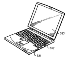
図21は、電子機器の第3の例としてのノート型パーソナルコンピュータの外観を表したものである。このノート型パーソナルコンピュータは、例えば、本体531,文字等の入力操作のためのキーボード532および画像を表示する表示部533を有している。このようなノート型パーソナルコンピュータにおける表示部533に、上述の入力機能付き表示装置を適用することが可能である。
(Application example 3)
FIG. 21 illustrates an appearance of a notebook personal computer as a third example of the electronic apparatus. This notebook personal computer has, for example, a
(適用例4)
図22は、電子機器の第4の例としてのビデオカメラの外観を表したものである。このビデオカメラは、例えば、本体部541,この本体部541の前方側面に設けられた被写体撮影用のレンズ542,撮影時のスタート/ストップスイッチ543および表示部544を有している。このようなビデオカメラにおける表示部544に、上述の入力機能付き表示装置を適用することが可能である。
(Application example 4)
FIG. 22 illustrates an appearance of a video camera as a fourth example of the electronic apparatus. This video camera includes, for example, a
(適用例5)
図23(A)〜(G)は、電子機器の第5の例としての携帯電話機の外観を表したものである。この携帯電話機は、例えば、上側筐体710と下側筐体720とを連結部(ヒンジ部)730で連結したものであり、ディスプレイ740,サブディスプレイ750,ピクチャーライト760およびカメラ770を有している。このような携帯電話機におけるディスプレイ740またはサブディスプレイ750に、上述の入力機能付き表示装置を適用することが可能である。
(Application example 5)
FIGS. 23A to 23G show the appearance of a mobile phone as a fifth example of the electronic apparatus. For example, the mobile phone is obtained by connecting an
<第1の実施の形態の変形例>
本発明は上記第1の実施の形態、およびその適用例に限定されず種々の変形実施が可能である。例えば、上記第1の実施の形態等では、バックライト15を備えた液晶パネルからなるI/Oディスプレイパネル20の場合で説明したが、表示用のバックライトが検出用照明を兼ねてもよいし、検出専用の照明を設けてもよい。また、検出用照明を設ける場合には、可視光領域以外の波長領域の光(例えば、赤外光)を用いるのがより好ましい。
<Modification of the first embodiment>
The present invention is not limited to the first embodiment and application examples, and various modifications can be made. For example, in the first embodiment and the like, the case of the I /
さらに、上記第1の実施の形態等では、複数の表示画素31RGBと複数のセンサ素子33とを含む表示パネル(I/Oディスプレイパネル20)を有する入力機能付き表示装置について説明したが、本発明は表示装置以外にも適用可能である。例えば表示機能のない単なるセンサ装置としても適用可能である。この場合、例えばI/Oディスプレイパネル20に代えて、表示画素31RGBを設けずに複数のセンサ素子33のみを1つの面内にマトリクス状に配置することにより構成されたセンサパネルを備えるようにすれば良い。
Further, in the first embodiment and the like, the display device with an input function having the display panel (I / O display panel 20) including the plurality of display pixels 31RGB and the plurality of
<第2の実施の形態>
[放射線撮像装置の全体構成]
本実施の形態では、本発明を放射線撮像装置に適用した構成例について説明する。図24は、本実施の形態に係る放射線撮像装置101のうちの光電変換装置102のシステム構成を表すものである。放射線撮像装置101は、光電変換装置102の上に、図25に示したように、波長変換体140を設けたものである。放射線撮像装置101は、α線、β線、γ線、X線に代表される放射線を波長変換体140によって波長変換して放射線に基づく情報を読み取るようになっている。
<Second Embodiment>
[Overall configuration of radiation imaging apparatus]
In this embodiment, a configuration example in which the present invention is applied to a radiation imaging apparatus will be described. FIG. 24 illustrates a system configuration of the
波長変換体140は、上記のような放射線を光電変換装置102の感度域に波長変換するものである。波長変換体140は例えばX線などの放射線を、放射線よりも波長の長い光(例えば可視光)に変換する蛍光体(例えば、シンチレータ)である。具体的には、有機平坦化膜、スピンオングラス材料等からなる平坦化膜の上面にCsI、NaI、CaF2等の蛍光体膜を形成したものである。
The
光電変換装置102は、基板111上に画素部112を有し、この画素部112の周囲に、例えば行走査部(垂直駆動部)113、水平選択部114、列走査部(水平駆動部)115およびシステム制御部116からなる周辺回路部(駆動部)が設けられている。
The
画素部112には、入射光の光量に応じた電荷量の光電荷を発生して内部に蓄積する光電変換部(後述する光電変換素子PD11)を有する単位画素120(以下、単に「画素」と記述する場合もある)が複数、行列状に2次元配置されている。
The
画素部112には更に、行列状の画素配列に対して画素行ごとに画素駆動線117が行方向(画素行の画素の配列方向)に沿って配線され、画素列ごとに垂直信号線(読み出し線)118が列方向(画素列の画素の配列方向)に沿って配線されている。画素駆動線117は、画素からの信号読み出しのための駆動信号を伝送するものである。画素駆動線117としては例えば、後述する図26等の画素回路に接続されるリード制御信号線Readおよびリセット制御信号線Resetが画素行ごとに設けられている。画素駆動線117の一端は、行走査部113の各行に対応した出力端に接続されている。
The
行走査部113は、シフトレジスタやアドレスデコーダ等によって構成され、画素部112の各画素を、例えば行単位で駆動する画素駆動部である。行走査部113によって選択走査された画素行の各単位画素から出力される信号は、垂直信号線118の各々を通して水平選択部114に供給される。水平選択部114は、垂直信号線118ごとに設けられたアンプや水平選択スイッチ等によって構成されている。
The
列走査部115は、シフトレジスタやアドレスデコーダ等によって構成され、水平選択部114の各水平選択スイッチを走査しつつ順番に駆動する。この列走査部115による選択走査により、垂直信号線118の各々を通して伝送される各画素の信号が順番に水平信号線119に出力され、当該水平信号線119を通して基板111の外部へ伝送される。
The
行走査部113、水平選択部114、列走査部115および水平信号線119からなる回路部分は、基板111上に形成された回路もしくは外部制御ICあるいはその両方を併用して構成される。あるいは、それらの回路部分は、ケーブル等により接続された他の基板に形成されていてもよい。
A circuit portion including the
システム制御部116は、基板111の外部から与えられるクロックや、動作モードを指令するデータなどを受け取り、また、光電変換装置102の内部情報などのデータを出力する。システム制御部116はさらに、各種のタイミング信号を生成するタイミングジェネレータを有し、当該タイミングジェネレータで生成された各種のタイミング信号を基に行走査部113、水平選択部114および列走査部115などの周辺回路部の駆動制御を行う。
The
[単位画素120(センサ素子)の回路構成]
単位画素120の回路構成としては、アクティブ型とパッシブ型とがある。以下、図26〜図29を参照して、それぞれのタイプの回路構成例を説明する。
[Circuit Configuration of Unit Pixel 120 (Sensor Element)]
The circuit configuration of the
(アクティブ型の画素回路の第1の構成例)
図26は、単位画素120をアクティブ型の画素回路で構成した第1の構成例を示している。このアクティブ型の第1の構成例では、単位画素120に、光電変換素子PD11、蓄積ノードN(電荷蓄積部)、リセット用トランジスタTr11、増幅用トランジスタTr12および選択・読み出し用トランジスタTr13が設けられている。この単位画素120に対して、画素駆動線117として例えば2本の配線、具体的にはリード制御信号線Readおよびリセット制御信号線Resetが画素行ごとに配線されている。
(First Configuration Example of Active Pixel Circuit)
FIG. 26 shows a first configuration example in which the
光電変換素子PD11は、入射光量に応じた電荷を発生させるものであり、例えばPIN型のフォトダイオードにより構成されている。PIN型のフォトダイオードは、後述の図30に示すように、p型半導体領域(p型半導体層164)と、n型半導体領域(n型半導体層171)と、p型半導体領域とn型半導体領域との間に形成された真性半導体領域(i型半導体層170)とを有するものである。光電変換素子PD11において、p型半導体領域にはアノード電極が接続され、n型半導体領域にはカソード電極が接続されている。光電変換素子PD11のカソード電極は、電源電圧VDDを供給する電源線SVDDに接続されている。光電変換素子PD11の一端(アノード電極)は、リセット用トランジスタTr11の一端(ドレイン端子)に接続されている。 The photoelectric conversion element PD11 generates an electric charge according to the amount of incident light, and is composed of, for example, a PIN type photodiode. As shown in FIG. 30 described later, the PIN photodiode includes a p-type semiconductor region (p-type semiconductor layer 164), an n-type semiconductor region (n-type semiconductor layer 171), a p-type semiconductor region, and an n-type semiconductor. And an intrinsic semiconductor region (i-type semiconductor layer 170) formed between the regions. In the photoelectric conversion element PD11, an anode electrode is connected to the p-type semiconductor region, and a cathode electrode is connected to the n-type semiconductor region. The cathode electrode of the photoelectric conversion element PD11 is connected to a power supply line SVDD that supplies a power supply voltage VDD. One end (anode electrode) of the photoelectric conversion element PD11 is connected to one end (drain terminal) of the reset transistor Tr11.
蓄積ノードNは、光電変換素子PD11の一端(アノード電極)とリセット用トランジスタTr11の一端(ドレイン端子)と増幅用トランジスタTr12のゲート端子とに接続されている。蓄積ノードNには、光電変換素子PD11によって変換された電荷が蓄積されるようになっている。蓄積ノードNの電圧値Vsは、蓄積電荷に応じて電圧変動するようになっている。 The storage node N is connected to one end (anode electrode) of the photoelectric conversion element PD11, one end (drain terminal) of the reset transistor Tr11, and the gate terminal of the amplification transistor Tr12. The storage node N stores charges converted by the photoelectric conversion element PD11. The voltage value Vs of the storage node N varies in voltage according to the stored charge.
リセット用トランジスタTr11、増幅用トランジスタTr12および選択・読み出し用トランジスタTr13はそれぞれ、例えば薄膜トランジスタ(TFT;ThinFilm Transistor)などにより構成されている。 Each of the resetting transistor Tr11, the amplifying transistor Tr12, and the selection / reading transistor Tr13 includes, for example, a thin film transistor (TFT).
リセット用トランジスタTr11のゲート端子はリセット制御信号V(Reset)を供給するリセット制御信号線Resetに接続され、ソース端子は所定の電圧(リセット電圧Vrst)の供給線SVSSに接続されている。リセット用トランジスタTr11のドレイン端子および増幅用トランジスタTr12のゲート端子は、蓄積ノードNに接続されている。増幅用トランジスタTr12のドレイン端子は、電源電圧VDDを供給する電源線SVDDに接続されている。増幅用トランジスタTr12のソース端子は、選択・読み出し用トランジスタTr13のドレイン端子に接続されている。選択・読み出し用トランジスタTr13のゲート端子は、リード制御信号V(Read)を供給するリード制御信号線Readに接続され、ソース端子は読み出し線41に接続されている。
The gate terminal of the reset transistor Tr11 is connected to a reset control signal line Reset that supplies a reset control signal V (Reset), and the source terminal is connected to a supply line SVSS of a predetermined voltage (reset voltage Vrst). The drain terminal of the resetting transistor Tr11 and the gate terminal of the amplifying transistor Tr12 are connected to the storage node N. The drain terminal of the amplifying transistor Tr12 is connected to the power supply line SVDD that supplies the power supply voltage VDD. The source terminal of the amplifying transistor Tr12 is connected to the drain terminal of the selection / reading transistor Tr13. The selection / reading transistor Tr13 has a gate terminal connected to a read control signal line Read that supplies a read control signal V (Read), and a source terminal connected to a read
リセット用トランジスタTr11は、蓄積ノードNに所定のリセット電圧Vrstを与えることにより、蓄積ノードNの電圧値Vsを所定のリセット電圧Vrstにリセットする(蓄積ノードNの蓄積電荷を放出させる)ためのものである。本実施の形態では、図24の行走査部113およびシステム制御部116が、後述の動作タイミング例(図31、図33等)に示すように、リセット用トランジスタTr11のゲート端子に印加するリセット制御信号V(Reset)のパルス期間を制御することにより、所定のリセット電圧Vrstが1H(水平走査)期間を超える期間に亘って連続または間欠的に蓄積ノードNに与えられるようになっている。
The reset transistor Tr11 applies a predetermined reset voltage Vrst to the storage node N, thereby resetting the voltage value Vs of the storage node N to a predetermined reset voltage Vrst (to release the stored charge of the storage node N). It is. In this embodiment, the reset control applied by the
増幅用トランジスタTr12と選択・読み出し用トランジスタTr13は、信号読み出し回路を形成し、蓄積ノードNの蓄積電荷に応じた電圧値を読み出してセンサ検出信号として出力するようになっている。センサ検出信号は、選択・読み出し用トランジスタTr3がゲート端子に印加されたリード制御信号V(Read)に応じてオンされたタイミングで、垂直信号線(読み出し線)118に出力される(読み出される)ようになっている。
増幅用トランジスタTr12と選択・読み出し用トランジスタTr13は、本発明における「読み出し手段」の一具体例に対応している。
The amplifying transistor Tr12 and the selection / reading transistor Tr13 form a signal reading circuit, and a voltage value corresponding to the accumulated charge at the accumulation node N is read and output as a sensor detection signal. The sensor detection signal is output (read) to the vertical signal line (read line) 118 at a timing when the selection / read transistor Tr3 is turned on in response to the read control signal V (Read) applied to the gate terminal. It is like that.
The amplifying transistor Tr12 and the selection / reading transistor Tr13 correspond to a specific example of “reading means” in the present invention.
垂直信号線118の一端には定電流源131が接続されている。垂直信号線118にはまた、図24の水平選択部114の入力部を構成するアンプ133が接続されている。垂直信号線118に出力された信号は、画素列ごとにアンプ33に入力される。
A constant
(アクティブ型の画素回路の第2の構成例)
図27は、単位画素120をアクティブ型の画素回路で構成した第2の構成例を示している。この第2の構成例では、アクティブ型の第1の構成例(図26)に対して、光電変換素子PD11とリセット用トランジスタTr11との位置関係が異なっている。第1の構成例では光電変換素子PD11のアノード電極(p型半導体領域)とリセット用トランジスタTr11のドレイン端子との間に蓄積ノードNが形成されていたが、この第2の構成例では、光電変換素子PD11のカソード電極(n型半導体領域)とリセット用トランジスタTr11のドレイン端子との間に蓄積ノードNが形成されている。また、リセット用トランジスタTr11のソース端子は、電源電圧VDDを供給する電源線SVDDに接続されている。光電変換素子PD11のアノード電極は、所定の電圧を供給する電源線SVSSに接続されている。
(Second Configuration Example of Active Pixel Circuit)
FIG. 27 shows a second configuration example in which the
(パッシブ型の画素回路の第1の構成例)
図28は、単位画素120をパッシブ型の画素回路で構成した第1の構成例を示している。このパッシブ型の第1の構成例では、単位画素120が、光電変換素子PD11、蓄積ノードN、および選択・読み出し用トランジスタTr13で構成されている。垂直信号線118には、図24の水平選択部114の入力部を構成するチャージアンプ回路が接続されている。チャージアンプ回路は、キャパシタ(フィードバック容量)191と、チャージアンプ192と、スイッチ193とからなる。
(First configuration example of passive pixel circuit)
FIG. 28 shows a first configuration example in which the
蓄積ノードNは、光電変換素子PD11のアノード電極(p型半導体領域)と選択・読み出し用トランジスタTr13のドレイン端子との間に形成されている。光電変換素子PD11のカソード電極(n型半導体領域)は、電源電圧VDDを供給する電源線SVDDに接続されている。 The storage node N is formed between the anode electrode (p-type semiconductor region) of the photoelectric conversion element PD11 and the drain terminal of the select / read transistor Tr13. The cathode electrode (n-type semiconductor region) of the photoelectric conversion element PD11 is connected to the power supply line SVDD that supplies the power supply voltage VDD.
(パッシブ型の画素回路の第2の構成例)
図29は、単位画素120をパッシブ型の画素回路で構成した第2の構成例を示している。この第2の構成例では、パッシブ型の第1の構成例(図28)に対して、蓄積ノードNと光電変換素子PD11との位置関係が異なっている。この第2の構成例では、蓄積ノードNは、光電変換素子PD11のカソード電極(n型半導体領域)と選択・読み出し用トランジスタTr13のドレイン端子との間に形成されている。光電変換素子PD11のアノード電極(p型半導体領域)は、所定の電圧を供給する電源線SVSSに接続されている。
(Second configuration example of passive pixel circuit)
FIG. 29 shows a second configuration example in which the
図28および図29のパッシブ型の画素回路では、図26および図27のアクティブ型の画素回路とは異なり、リセット用トランジスタTr11は設けられていない。また、リセット動作時には、リセット制御信号V(Reset)は用いられない。このパッシブ型の画素回路では、センサ検出信号の読み出し動作と蓄積ノードNの通常のリセット動作とが実質的に同時に行われる。読み出し動作は、選択・読み出し用トランジスタTr3がゲート端子に印加されたリード制御信号V(Read)に応じてオンされたタイミングで行われる。選択・読み出し用トランジスタTr3がオンされると、蓄積ノードNの蓄積電荷がチャージアンプ回路のキャパシタ191に蓄積され、その蓄積電荷に応じた信号電圧がチャージアンプ192から出力される(読み出される)。この読み出し動作に伴い、蓄積ノードNの蓄積電荷が所定のリセット電圧Vrstにリセットされる。チャージアンプ回路のスイッチ193は読み出し動作前にはオン状態にあり、読み出し動作時にはオフ状態とされる。チャージアンプ回路のキャパシタ191に蓄積された電荷は、スイッチ193をオン状態にすることでリセットされる。
In the passive pixel circuits of FIGS. 28 and 29, unlike the active pixel circuits of FIGS. 26 and 27, the reset transistor Tr11 is not provided. In the reset operation, the reset control signal V (Reset) is not used. In this passive pixel circuit, the sensor detection signal readout operation and the normal reset operation of the storage node N are performed substantially simultaneously. The read operation is performed at the timing when the selection / read transistor Tr3 is turned on according to the read control signal V (Read) applied to the gate terminal. When the selection / readout transistor Tr3 is turned on, the accumulated charge of the accumulation node N is accumulated in the
このように、パッシブ型の画素回路では、読み出し動作が通常のリセット動作を兼ねているが、選択・読み出し用トランジスタTr3を読み出し動作時と同様にオン状態にした状態で、チャージアンプ回路のスイッチ193をオン状態にすることで別途、追加のリセット動作を間欠的に行うことができる。本実施の形態では、図24の行走査部113およびシステム制御部116が、後述の動作タイミング例(図32、図34等)に示すような動作タイミングとなるように制御することにより、パッシブ型の画素回路であっても所定のリセット電圧Vrstが1H(水平走査)期間を超える期間に亘って間欠的に蓄積ノードNに与えられるようになっている。
As described above, in the passive pixel circuit, the read operation also serves as a normal reset operation. However, the
なお、上記した例に限らず、パッシブ型の画素回路において、例えば垂直信号線118にリセット用の切り換えスイッチを別途設け、その切り換えスイッチの切り換え動作によってリセット動作を行うようにしても良い。
Note that the present invention is not limited to the above example. In a passive pixel circuit, for example, a reset changeover switch may be separately provided on the
[画素の断面構造]
図4は光電変換装置102の要部(単位画素120)の断面構造を表すものである。ここでは、単位画素120が、アクティブ型の第1の構成例(図26)である場合を例に挙げて説明する。
[Cross-sectional structure of pixel]
FIG. 4 illustrates a cross-sectional structure of a main part (unit pixel 120) of the
この光電変換装置102では、ガラス基板などの絶縁性基板161上に、Ti、Al、Mo、W、Cr等からなるゲート電極162が形成され、このゲート電極162上にはSiNx、SiO2等からなるゲート絶縁膜163が形成されている。ゲート絶縁膜163の上には、PIN型のフォトダイオード(光電変換素子PD11)を構成する例えばp型半導体層(p+領域)164(第1半導体層)が形成されている。
In this
p型半導体層164は、光電変換素子PD11で光電変換された信号電荷を読み出すための下部電極を兼ねている。ゲート絶縁膜163上にはさらに、増幅用トランジスタTr12等の画素トランジスタの半導体層165が形成されている。半導体層165には、リーク電流を低減するためにチャネル領域とドレイン・ソース領域との間にLDD(Lightly Doped Drain)165a,165bが設けられている。半導体層165は例えば微結晶シリコンあるいは多結晶シリコンにより構成されている。
The p-
p型半導体層164および画素トランジスタの半導体層165の上にはSiNx、SiO2等からなる第1層間絶縁膜166が設けられている。第1層間絶縁膜166の上部には、読出し用の信号線や各種の配線を含む配線層167がTi、Al、Mo、W、Cr等によって形成されている。配線層167の上にはSiNx,SiO2、有機絶縁膜等からなる第2の層間絶縁膜168が設けられている。
A first interlayer insulating film 166 made of SiNx, SiO 2 or the like is provided on the p-
第1,第2層間絶縁膜166,168からなる絶縁層には、コンタクトホール169が形成されている。第2層間絶縁膜168の上にはp型とn型の間の導電型からなる第3半導体層(i型半導体層170)が形成されている。このi型半導体層170の面積はコンタクトホール169の上部側の開口面積よりも大きくなっている。i型半導体層170はp型半導体層164とコンタクトホール169を介して接している。
A
i型半導体層170の上には、このi型半導体層170とほぼ同一形状の第2半導体層(例えばn型半導体層(n+領域)171)が積層されている。これらp型半導体層164(第1半導体層)、i型半導体層170(第3半導体層)およびn型半導体層171(第2半導体層)により光電変換素子PD11(PIN型のフォトダイオード)が構成されている。
このように、上記第1の実施の形態では面内方向(水平方向)にPIN構造が形成された光電変換素子PD1(図6参照)の例を挙げたが、本実施の形態では、光電変換素子PD11は、積層方向(光の入射方向に対して垂直方向)にPIN構造が形成されている。
On the i-type semiconductor layer 170, a second semiconductor layer (for example, an n-type semiconductor layer (n + region) 171) having substantially the same shape as the i-type semiconductor layer 170 is stacked. The p-type semiconductor layer 164 (first semiconductor layer), the i-type semiconductor layer 170 (third semiconductor layer), and the n-type semiconductor layer 171 (second semiconductor layer) constitute a photoelectric conversion element PD11 (PIN type photodiode). Has been.
As described above, in the first embodiment, the example of the photoelectric conversion element PD1 (see FIG. 6) in which the PIN structure is formed in the in-plane direction (horizontal direction) has been described. However, in the present embodiment, the photoelectric conversion is performed. The element PD11 has a PIN structure formed in the stacking direction (perpendicular to the light incident direction).
この光電変換素子PD11において、各半導体層164,170,171はアモルファスシリコン、微結晶シリコン、多結晶シリコンなどで形成することができる。これらのシリコンに、ゲルマニウムや炭素などの材料を導入して、分光感度を変えるようにしてもよい。光電変換素子PD11としては、下部側をn型、上部側をp型にするような逆向きの構成でも構わない。 In the photoelectric conversion element PD11, the semiconductor layers 164, 170, and 171 can be formed of amorphous silicon, microcrystalline silicon, polycrystalline silicon, or the like. Spectral sensitivity may be changed by introducing a material such as germanium or carbon into these silicon. The photoelectric conversion element PD11 may have a reverse configuration in which the lower side is n-type and the upper side is p-type.
n型半導体層171の上には、光電変換素子PD11に対して規定の電圧を印加するための上部電極172がITO(Indium Tin Oxide)等の透明導電膜によって形成されている。上部電極172の上には、この上部電極172に電圧を供給するための電源配線173が設けられている。電源配線173は上部電極172の透明導電膜よりも低抵抗の材料、即ちTi、Al、Mo、W、Cr等によって構成されている。この電源配線173は、例えば単位画素120を囲むようにメッシュ状に画素部112の全面に亘って形成される。この上部電極172上には更に、SiN等からなる保護膜(図示せず)が形成されていてもよい。
On the n-type semiconductor layer 171, an upper electrode 172 for applying a prescribed voltage to the photoelectric conversion element PD11 is formed of a transparent conductive film such as ITO (Indium Tin Oxide). A
[読み出し動作、リセット動作のタイミング例]
(アクティブ型の画素回路に適用される動作タイミングの第1の例)
図31は、図26および図27に示したアクティブ型の画素回路を適用した光電変換装置102の撮像動作のタイミングの第1の例を示している。また、図33は、図31に示した動作タイミングに対応するタイミングチャートを示している。図31の上部に示した上方から下方に延びる矢印は、光電変換装置102の動作タイミングを模式的に示している。横方向は時間、縦方向は画素部112(図24)の走査ラインに相当する。図31では、上側の水平ラインから下側の水平ラインに向けて線順次で読み出し動作(走査)を行う例を示している。図31において「Read」は読み出し動作を行うことを表し、「Reset」は通常(1回目)のリセット動作を行うことを表す。「Ex−Reset」は1フレーム期間内で追加(2回目)のリセット動作を行うことを表す。「X−ray」は、画素部112に放射線(例えばX線)が照射される撮像期間(露光期間)を表す。
[Timing example of read operation and reset operation]
(First example of operation timing applied to an active pixel circuit)
FIG. 31 illustrates a first example of the imaging operation timing of the
図31に示したように、上ラインから下ラインまで順次、読み出し動作を行いつつ、所定期間を空けて通常(1回目)のリセット動作を上ラインから下ラインまで順次、行う。次いで、所定期間を空けて追加(2回目)のリセット動作を上ラインから下ラインまで順次、行う。これらを1フレーム期間内に行う。読み出し動作は、選択・読み出し用トランジスタTr13のゲート端子にリード制御信号V(Read)が印加されたタイミングで行われる。リセット動作は、リセット用トランジスタTr11のゲート端子にリセット制御信号V(Reset)が印加されたタイミングで行われる。 As shown in FIG. 31, while performing the read operation sequentially from the upper line to the lower line, the normal (first) reset operation is sequentially performed from the upper line to the lower line after a predetermined period. Next, an additional (second) reset operation is sequentially performed from the upper line to the lower line after a predetermined period. These are performed within one frame period. The read operation is performed at the timing when the read control signal V (Read) is applied to the gate terminal of the selection / read transistor Tr13. The reset operation is performed at the timing when the reset control signal V (Reset) is applied to the gate terminal of the reset transistor Tr11.
図33には、リセット用トランジスタTr11のゲート端子に印加されるリセット制御信号V(Reset)の印加タイミングと、選択・読み出し用トランジスタTr13のゲート端子に印加されるリード制御信号V(Read)の印加タイミングとを、それぞれ6水平ライン分、示している。例えば最も上側の第1水平ライン上のリセット用トランジスタTr11のゲート端子に印加されるリセット制御信号V(Reset)をV(Reset1)とし、次の下側の第2水平ライン上のリセット用トランジスタTr11のゲート端子に印加されるリセット制御信号V(Reset)をV(Reset2)としている。図31および図33の動作タイミング例では、1フレーム期間内で、読み出し動作後に2回のリセット動作が行われる。これにより、リセット用トランジスタTr11のゲート端子にリセット制御信号V(Reset)として、1H(水平走査)期間を超える期間内に2つの間欠的な電圧パルス信号が印加されるようにしている。これにより、所定のリセット電圧Vrstが1H期間を超える期間に亘って間欠的に蓄積ノードNに与えられるようにしている。 FIG. 33 shows the application timing of the reset control signal V (Reset) applied to the gate terminal of the reset transistor Tr11 and the application of the read control signal V (Read) applied to the gate terminal of the selection / read transistor Tr13. The timing is shown for 6 horizontal lines each. For example, the reset control signal V (Reset) applied to the gate terminal of the reset transistor Tr11 on the uppermost first horizontal line is V (Reset1), and the reset transistor Tr11 on the next lower second horizontal line is set. The reset control signal V (Reset) applied to the gate terminal of V is set to V (Reset2). In the operation timing examples of FIGS. 31 and 33, two reset operations are performed after the read operation within one frame period. Thus, two intermittent voltage pulse signals are applied to the gate terminal of the reset transistor Tr11 as a reset control signal V (Reset) within a period exceeding 1H (horizontal scanning) period. Thus, the predetermined reset voltage Vrst is intermittently supplied to the storage node N over a period exceeding 1H period.
なお、図31では、1フレーム期間内で2回のリセット動作を行う例を示しているが、読み出し動作後に、1フレーム期間内で3回以上のリセット動作を行うようにしても良い。 FIG. 31 shows an example in which the reset operation is performed twice within one frame period. However, the reset operation may be performed three times or more within one frame period after the read operation.
(パッシブ型の画素回路に適用される動作タイミングの第1の例)
図32は、図28および図29に示したパッシブ型の画素回路を適用した光電変換装置102の撮像動作のタイミングの第1の例を示している。また、図34は、図32に示した動作タイミングに対応するタイミングチャートを示している。図32の例では図31の例と同様、上側の水平ラインから下側の水平ラインに向けて線順次で読み出し動作(走査)を行う例を示している。図31の例と同様、図32において「Read」は読み出し動作を行うことを表し、「Reset」は通常(1回目)のリセット動作を行うことを表す。「Ex−Reset」は1フレーム期間内で追加(2回目)のリセット動作を行うことを表す。「X−ray」は、画素部112に放射線(例えばX線)が照射される撮像期間(露光期間)を表す。なお、上述したようにパッシブ型の画素回路では、読み出し動作が通常のリセット動作を兼ねているので、読み出し動作と1回目のリセット動作とを同じタイミングとして示している。
(First example of operation timing applied to a passive pixel circuit)
FIG. 32 illustrates a first example of the timing of the imaging operation of the
図32に示したように、上ラインから下ラインまで順次、読み出し動作を行う。このとき、同時に通常(1回目)のリセット動作が上ラインから下ラインまで順次、行われる。次いで、所定期間を空けて追加(2回目)のリセット動作を上ラインから下ラインまで順次、行う。これらを1フレーム期間内に行う。読み出し動作は、上述したように、例えば選択・読み出し用トランジスタTr13のゲート端子にリード制御信号V(Read)をオン状態にし、チャージアンプ回路のスイッチ193をオフ状態にすることで行われる。追加のリセット動作は、例えば、選択・読み出し用トランジスタTr3を読み出し動作時と同様にオン状態にした状態で、チャージアンプ回路のスイッチ193をオン状態にすることで行われる。
As shown in FIG. 32, the read operation is sequentially performed from the upper line to the lower line. At this time, the normal (first time) reset operation is performed sequentially from the upper line to the lower line. Next, an additional (second) reset operation is sequentially performed from the upper line to the lower line after a predetermined period. These are performed within one frame period. As described above, the read operation is performed, for example, by turning on the read control signal V (Read) at the gate terminal of the select / read transistor Tr13 and turning off the
図34には、選択・読み出し用トランジスタTr13のゲート端子に印加されるリード制御信号V(Read)の印加タイミングを6水平ライン分、示している。図32および図34の動作タイミング例では、1フレーム期間内で、読み出し動作後に2回のリセット動作が行われる。これにより、所定のリセット電圧Vrstが1H期間を超える期間に亘って間欠的に蓄積ノードNに与えられるようにしている。 FIG. 34 shows the application timing of the read control signal V (Read) applied to the gate terminal of the selection / readout transistor Tr13 for six horizontal lines. 32 and FIG. 34, the reset operation is performed twice after the read operation within one frame period. Thus, the predetermined reset voltage Vrst is intermittently supplied to the storage node N over a period exceeding 1H period.
なお、図32では、1フレーム期間内で2回のリセット動作を行う例を示しているが、読み出し動作後に、1フレーム期間内で3回以上のリセット動作を行うようにしても良い。 Note that although FIG. 32 shows an example in which the reset operation is performed twice within one frame period, the reset operation may be performed three or more times within one frame period after the read operation.
(アクティブ型の画素回路に適用される動作タイミングの第2の例)
図35は、図26および図27に示したアクティブ型の画素回路を適用した光電変換装置102の撮像動作のタイミングの第2の例を示している。また、図36は、図35に示した動作タイミングに対応するタイミングチャートを示している。図35の例では図31の例と同様、上側の水平ラインから下側の水平ラインに向けて線順次で読み出し動作(走査)を行う例を示している。図31の例と同様、図32において「Read」は読み出し動作を行うことを表し、「Reset」はリセット動作を行うことを表す。「X−ray」は、画素部112に放射線(例えばX線)が照射される撮像期間(露光期間)を表す。
(Second example of operation timing applied to an active pixel circuit)
FIG. 35 illustrates a second example of the imaging operation timing of the
図35に示したように、上ラインから下ラインまで順次、読み出し動作を行いつつ、所定期間を空けてリセット動作を上ラインから下ラインまで順次、行う。図36には、リセット用トランジスタTr11のゲート端子に印加されるリセット制御信号V(Reset)の印加タイミングと、選択・読み出し用トランジスタTr13のゲート端子に印加されるリード制御信号V(Read)の印加タイミングとを、図33の例と同様、それぞれ6水平ライン分、示している。図35および図36の動作タイミング例では、1フレーム期間内で、読み出し動作後に1回のみリセット動作が行われる。そして、この1回のリセット動作によって、リセット用トランジスタTr11のゲート端子にリセット制御信号V(Reset)として、1H(水平走査)期間を超える連続的な電圧パルス信号が印加されるようにしている。これにより、所定のリセット電圧Vrstが1H期間を超える期間に亘って連続的に蓄積ノードNに与えられるようにしている。 As shown in FIG. 35, the read operation is sequentially performed from the upper line to the lower line, and the reset operation is sequentially performed from the upper line to the lower line after a predetermined period. 36 shows the application timing of the reset control signal V (Reset) applied to the gate terminal of the reset transistor Tr11 and the application of the read control signal V (Read) applied to the gate terminal of the selection / read transistor Tr13. The timing is shown for 6 horizontal lines, as in the example of FIG. 35 and 36, the reset operation is performed only once after the read operation within one frame period. With this one reset operation, a continuous voltage pulse signal exceeding the 1H (horizontal scanning) period is applied as the reset control signal V (Reset) to the gate terminal of the reset transistor Tr11. Thus, the predetermined reset voltage Vrst is continuously applied to the storage node N over a period exceeding 1H period.
(アクティブ型の画素回路に適用される動作タイミングの第3の例)
図37は、図26および図27に示したアクティブ型の画素回路を適用した光電変換装置102の撮像動作のタイミングの第3の例を示している。図36の例では図31の例と同様、上側の水平ラインから下側の水平ラインに向けて線順次で読み出し動作(走査)を行う例を示している。図31の例と同様、図32において「Read」は読み出し動作を行うことを表し、「Reset」は通常(1回目)のリセット動作を行うことを表す。「Ex−Reset」は1フレーム期間内で追加(2回目)のリセット動作を行うことを表す。「X−ray」は、画素部112に放射線(例えばX線)が照射される撮像期間(露光期間)を表す。これにより、図31および図33の動作タイミング例と同様に、1フレーム期間内で、読み出し動作後に2回のリセット動作が行われる。これにより、リセット用トランジスタTr11のゲート端子にリセット制御信号V(Reset)として、1H(水平走査)期間を超える期間内に2つの間欠的な電圧パルス信号が印加されるようにしている。これにより、所定のリセット電圧Vrstが1H期間を超える期間に亘って間欠的に蓄積ノードNに与えられるようにしている。
(Third example of operation timing applied to an active pixel circuit)
FIG. 37 illustrates a third example of the timing of the imaging operation of the
図37に示したように、上ラインから下ラインまで順次、読み出し動作を行いつつ、所定期間を空けて通常(1回目)のリセット動作を上ラインから下ラインまで行う。次いで、所定期間を空けて追加(2回目)のリセット動作を行う。ここで、図31の例では2回目のリセット動作を上ラインから下ラインまで線順次で行うようにしていたが、図37の例では、全画素分、一括してリセット動作を行うようにしている。このときのリセット動作は、全画素分のリセット用トランジスタTr11のゲート端子にリセット制御信号V(Reset)を印加することで行われる。 As shown in FIG. 37, while performing a read operation sequentially from the upper line to the lower line, a normal (first) reset operation is performed from the upper line to the lower line after a predetermined period. Next, an additional (second) reset operation is performed after a predetermined period. Here, in the example of FIG. 31, the second reset operation is performed line-sequentially from the upper line to the lower line, but in the example of FIG. 37, the reset operation is performed collectively for all pixels. Yes. The reset operation at this time is performed by applying a reset control signal V (Reset) to the gate terminals of the reset transistors Tr11 for all pixels.
(パッシブ型の画素回路に適用される動作タイミングの第2の例)
図38は、図28および図29に示したパッシブ型の画素回路を適用した光電変換装置102の撮像動作のタイミングの第2の例を示している。図38の例では図31の例と同様、上側の水平ラインから下側の水平ラインに向けて線順次で読み出し動作(走査)を行う例を示している。図31の例と同様、図38において「Read」は読み出し動作を行うことを表し、「Reset」は通常(1回目)のリセット動作を行うことを表す。「Ex−Reset」は1フレーム期間内で追加(2回目)のリセット動作を行うことを表す。「X−ray」は、画素部112に放射線(例えばX線)が照射される撮像期間(露光期間)を表す。なお、上述したようにパッシブ型の画素回路では、読み出し動作が通常のリセット動作を兼ねているので、読み出し動作と1回目のリセット動作とを同じタイミングとして示している。
(Second example of operation timing applied to passive pixel circuit)
FIG. 38 illustrates a second example of the imaging operation timing of the
図38に示したように、上ラインから下ラインまで順次、読み出し動作を行う。このとき、同時に通常(1回目)のリセット動作が上ラインから下ラインまで順次、行われる。次いで、所定期間を空けて追加(2回目)のリセット動作を行う。ここで、図32の例では2回目のリセット動作を上ラインから下ラインまで線順次で行うようにしていたが、図38の例では、全画素分、一括してリセット動作を行うようにしている。このときのリセット動作は、全画素分について、例えば、選択・読み出し用トランジスタTr3を読み出し動作時と同様にオン状態にした状態で、チャージアンプ回路のスイッチ193をオン状態にすることで行われる。
As shown in FIG. 38, the read operation is sequentially performed from the upper line to the lower line. At this time, the normal (first time) reset operation is performed sequentially from the upper line to the lower line. Next, an additional (second) reset operation is performed after a predetermined period. Here, in the example of FIG. 32, the second reset operation is performed line-sequentially from the upper line to the lower line, but in the example of FIG. 38, the reset operation is performed collectively for all pixels. Yes. The reset operation at this time is performed, for example, by turning on the
[リセット期間の長さと残像(残電圧)との関係]
次に、放射線撮像装置におけるリセット期間の長さ(所定のリセット電圧Vrstを蓄積ノードNに与える期間)と残像(残電圧)との関係について考察する。
[Relationship between reset period length and afterimage (residual voltage)]
Next, the relationship between the length of the reset period (period in which the predetermined reset voltage Vrst is applied to the storage node N) and the afterimage (residual voltage) in the radiation imaging apparatus will be considered.
図39は、アクティブ型の画素回路に適用される動作タイミングの第1の比較例を示している。この第1の比較例は、図31に示した動作タイミング例に対して2回目のリセット動作を省略したものである。図40は、アクティブ型の画素回路に適用される動作タイミングの第2の比較例を示している。この第2の比較例では、図39の第1の比較例に対して、読み出し動作が上ラインから下ラインまで全て完了した後に、リセット動作を行う例を示している。 FIG. 39 shows a first comparative example of operation timing applied to an active pixel circuit. In the first comparative example, the second reset operation is omitted from the operation timing example shown in FIG. FIG. 40 shows a second comparative example of the operation timing applied to the active pixel circuit. In the second comparative example, as compared with the first comparative example of FIG. 39, an example is shown in which the reset operation is performed after the read operation is completed from the upper line to the lower line.
図41は、パッシブ型の画素回路に適用される動作タイミングの第1の比較例を示している。このパッシブ型の画素回路に適用される第1の比較例は、図32に示した動作タイミング例に対して2回目のリセット動作を省略したものである。 FIG. 41 illustrates a first comparative example of operation timing applied to a passive pixel circuit. In the first comparative example applied to the passive pixel circuit, the second reset operation is omitted from the operation timing example shown in FIG.
(比較例の動作タイミングでの残電圧の測定結果)
これらの比較例の動作タイミングで放射線撮像装置を動作させた場合、リセット動作を行った後であっても、各画素からの出力電圧に残像(残電圧)が発生する。図45〜図48は、その残電圧を測定した結果を示している。
(Measurement result of residual voltage at operation timing of comparative example)
When the radiation imaging apparatus is operated at the operation timing of these comparative examples, an afterimage (residual voltage) is generated in the output voltage from each pixel even after the reset operation is performed. 45 to 48 show the results of measuring the residual voltage.
図42および図44は、その残電圧の測定に用いた動作タイミングを示している。図42は、アクティブ型の画素回路の特性検証用の動作タイミングを示している。基本的な動作タイミングは図39の比較例と同様であるが、残電圧を測定するために、図42および図44(A)に示したように10フレームの最初のフレームのみ測定用光源(LED)からの光照射(発光、露光動作)を行い、残りのフレームでは光照射が行われない非発光状態としている。リセット動作は、図42および図44(B)に示したように各フレームごとに行っている。なお、図45〜図48では、アクティブ型の画素回路の測定結果を示すが、パッシブ型の画素回路についても同様の測定結果が得られる。図43は、パッシブ型の画素回路の特性検証用の動作タイミングを示している。 42 and 44 show the operation timing used for measuring the residual voltage. FIG. 42 shows operation timings for verifying the characteristics of the active pixel circuit. The basic operation timing is the same as that of the comparative example of FIG. 39. However, in order to measure the residual voltage, only the first frame of 10 frames is measured as shown in FIGS. 42 and 44A. ) (Light emission, exposure operation) is performed, and the remaining frames are in a non-light emitting state in which no light irradiation is performed. The reset operation is performed for each frame as shown in FIG. 42 and FIG. 45 to 48 show the measurement results of the active pixel circuit, the same measurement results can be obtained for the passive pixel circuit. FIG. 43 shows operation timings for verifying the characteristics of the passive pixel circuit.
図45は、アクティブ型の画素回路の出力電圧を直接的に測定した結果を示す。この測定結果は、放射線撮像装置を構成する周辺回路を含めずに、画素回路の出力電圧を直接的に測定した結果である。縦軸は、残電圧の割合を示す。横軸はフレーム数に対応する経過時間を示すが、光照射を行ったフレームを基準にして、次のフレームを1番目のフレームとしている。図45では、測定用光源の発光量(光強度)を4段階に変えて測定した。4段階とは、光電変換素子PD11が飽和状態になるような強い光強度の場合と、中間的な光強度の場合と、光強度が弱い場合と、光強度がさらに弱い場合(弱弱)とを示す。この測定では、ノイズの影響による乱れが測定されているが、実質的に、光強度の違いによる残電圧の依存性はほとんど観測されなかった。 FIG. 45 shows the result of directly measuring the output voltage of the active pixel circuit. This measurement result is a result of directly measuring the output voltage of the pixel circuit without including the peripheral circuits constituting the radiation imaging apparatus. The vertical axis shows the ratio of the remaining voltage. The horizontal axis indicates the elapsed time corresponding to the number of frames, and the next frame is set as the first frame with reference to the frame irradiated with light. In FIG. 45, measurement was performed by changing the light emission amount (light intensity) of the measurement light source in four stages. The four stages are a case where the light intensity is such that the photoelectric conversion element PD11 is saturated, a case where the light intensity is intermediate, a case where the light intensity is weak, and a case where the light intensity is further weak (weak). Indicates. In this measurement, disturbance due to the influence of noise was measured, but substantially no dependency of the residual voltage due to the difference in light intensity was observed.
図46は、図27に示したアクティブ型の画素回路の第2の構成例(蓄積ノードNが光電変換素子PD11のカソード電極(n型半導体領域)側の構成例)において画素回路単体での出力電圧をアンプ133を通した後に測定した結果を示す特性図である。また、図47は、図26に示したアクティブ型の画素回路の第1の構成例(蓄積ノードNが光電変換素子PD11のアノード電極(p型半導体領域)側の構成例)において画素回路単体での出力電圧をアンプ133を通した後に測定した結果を示す特性図である。図45の測定結果は画素回路が放射線撮像装置に組み込まれた状態での測定結果であるが、図46および図47の測定結果は放射線撮像装置に組み込まれていない、画素回路単体(センサ素子単体)での測定結果である。図46(A),図47(A)では測定用光源の発光タイミングと、リセット制御信号V(Reset)の印加タイミングと、出力電圧とを同時に示す。図46(B),図47(B)は図46(A),図47(A)における出力電圧の波形部分を拡大したものである。図46(C),図47(C)はさらに、図46(B),図47(B)の出力電圧の波形部分を部分的に拡大したものである。図46,図47の測定結果から、光照射を行った後、1回目のリセット動作を行ったタイミングで一時的に所定のリセット電圧にリセットされる。しかしながら、その後、所定のリセット電圧が維持されずに、複数フレームに亘って波形に劣化(Decay)が生じてしまっている。この傾向は、蓄積ノードNが光電変換素子PD11のカソード電極(n型半導体領域)側にあるかアノード電極(p型半導体領域)側にあるかに関わらず生じている。
46 shows an output of a single pixel circuit in the second configuration example (configuration example where the storage node N is on the cathode electrode (n-type semiconductor region) side of the photoelectric conversion element PD11) of the active pixel circuit shown in FIG. It is a characteristic view showing the result of having measured the voltage after passing through the
図48(A)はアクティブ型の画素回路の第2の構成例において画素回路単体での出力電圧をアンプ133を通さずに直接的に検証した結果を示している。図48(B)はアクティブ型の画素回路の第1の構成例において画素回路単体での出力電圧をアンプ133を通さずに直接的に検証した結果を示している。図48(A),(B)において縦軸は残電圧の割合を示す。横軸はフレーム数に対応する経過時間を示すが、光照射を行ったフレームを基準にして、次のフレームを1番目のフレームとしている。図48(A),(B)は、図46および図47の測定結果と同様、放射線撮像装置に組み込まれていない、画素回路単体(センサ素子単体)での測定結果である。図48(A),(B)はではそれぞれ、複数の測定結果を同時に示しているが、それらは素子の製造条件の違いである。図48(A),(B)の測定結果から、光照射を行った後、2フレーム期間後ぐらいまでは残電圧の割合が比較的多く観測される。この傾向は、蓄積ノードNが光電変換素子PD11のカソード電極(n型半導体領域)側(図48(A))にあるかアノード電極(p型半導体領域)側(図48(B))にあるかに関わらず生じている。
FIG. 48A shows the result of directly verifying the output voltage of the pixel circuit alone without passing through the
(リセット動作を変えた場合の残電圧の測定結果)
以上の測定結果は、測定用光源(LED)からの光照射の発光タイミングとリセット動作のタイミング(リセット制御信号V(Reset)の印加タイミング)とが図49(A),(B)(図44(A),(B))に示したタイミングで行われたものであるが、これに対して図49(C)に示したように、リセット動作を行うタイミング(リセット間隔)を変えた場合の残電圧を測定した。その結果を図50に示す。1回のリセット動作の期間自体は図49(B)と同じである(4μsec)。図50において横軸は、放射線撮像装置の撮像動作におけるH(水平走査)期間を単位としたリセット間隔の時間を示す。ここでは1H(水平走査)期間=6μsecである。また、図50では、図27に示したアクティブ型の画素回路の第2の構成例(蓄積ノードNが光電変換素子PD11のカソード電極(n型半導体領域)側にある場合の構成例)での測定結果を示す。図50の結果から分かるようにリセット間隔を変えただけでは残電圧の特性に大きな変化は現れない。
(Measurement result of residual voltage when reset operation is changed)
The above measurement results show that the light emission timing of light irradiation from the measurement light source (LED) and the reset operation timing (application timing of the reset control signal V (Reset)) are as shown in FIGS. (A), (B)) is performed at the timing shown in FIG. 49C, but as shown in FIG. 49 (C), the reset operation timing (reset interval) is changed. The residual voltage was measured. The result is shown in FIG. The period of one reset operation itself is the same as that in FIG. 49B (4 μsec). In FIG. 50, the horizontal axis indicates the reset interval time in units of H (horizontal scanning) periods in the imaging operation of the radiation imaging apparatus. Here, 1H (horizontal scanning) period = 6 μsec. 50, in the second configuration example of the active pixel circuit shown in FIG. 27 (configuration example when the storage node N is on the cathode electrode (n-type semiconductor region) side of the photoelectric conversion element PD11). The measurement results are shown. As can be seen from the results of FIG. 50, a large change in the residual voltage characteristics does not appear only by changing the reset interval.
また、図49(D)に示したように、1フレーム期間内で間欠的に2回、リセット動作を行った場合の残電圧を測定した。その結果を図51(A)に示す。1回のリセット動作の期間自体は図49(B)と同じである(4μsec)。図51(A)において横軸は、放射線撮像装置の撮像動作におけるH(水平走査)期間を単位として、2回の間欠的なリセット動作を行う間隔を示す。ここでは1H(水平走査)期間=6μsecである。また、図51(A)では、図27に示したアクティブ型の画素回路の第2の構成例と、図26に示したアクティブ型の画素回路の第1の構成例(蓄積ノードNが光電変換素子PD11のアノード電極(p型半導体領域)側の構成例)との測定結果を同時に示す。図51(A)の結果から分かるように、間欠的に2回、リセット動作を行うことで、残電圧を減少させることができる。残電圧を減少させる効果は、1H期間を超える期間に亘って間欠的にリセット動作を行うことで得られている。特に、10H期間(60μsec)程度の間隔で間欠的に2回、リセット動作を行うことで、残電圧がほぼ半減している。 In addition, as shown in FIG. 49D, the residual voltage was measured when the reset operation was performed twice intermittently within one frame period. The result is shown in FIG. The period of one reset operation itself is the same as that in FIG. 49B (4 μsec). In FIG. 51A, the horizontal axis indicates an interval at which two intermittent reset operations are performed in units of H (horizontal scanning) periods in the imaging operation of the radiation imaging apparatus. Here, 1H (horizontal scanning) period = 6 μsec. In FIG. 51A, the second configuration example of the active pixel circuit shown in FIG. 27 and the first configuration example of the active pixel circuit shown in FIG. The measurement results with the configuration example on the anode electrode (p-type semiconductor region) side of the element PD11 are shown simultaneously. As can be seen from the result of FIG. 51A, the residual voltage can be reduced by performing the reset operation twice intermittently. The effect of reducing the residual voltage is obtained by performing the reset operation intermittently over a period exceeding 1H period. In particular, the residual voltage is almost halved by performing the reset operation twice intermittently at intervals of about 10H period (60 μsec).
また、図49(E)に示したように、1フレーム期間内で連続的なリセット動作を行った場合(連続的にリセット電圧を印加した場合)の残電圧を測定した。その結果を図51(B)に示す。図51(B)において横軸は、放射線撮像装置の撮像動作におけるH(水平走査)期間を単位として、1回の連続的なリセット動作を行う時間を示す。ここでは1H(水平走査)期間=6μsecである。また、図51(B)では、図27に示したアクティブ型の画素回路の第2の構成例と図26に示したアクティブ型の画素回路の第1の構成例との測定結果を同時に示す。図51(B)の結果から分かるように、連続的にリセット電圧を印加することで、残電圧を減少させることができる。残電圧を減少させる効果は、1H期間を超える期間に亘って連続的にリセット電圧を与えることで得られている。特に、10H期間(60μsec)程度の期間、連続的にリセット動作を行うことで、残電圧がほぼ半減している。 In addition, as shown in FIG. 49E, the residual voltage was measured when the continuous reset operation was performed within one frame period (when the reset voltage was applied continuously). The result is shown in FIG. In FIG. 51B, the horizontal axis indicates the time for one continuous reset operation in units of H (horizontal scanning) periods in the imaging operation of the radiation imaging apparatus. Here, 1H (horizontal scanning) period = 6 μsec. FIG. 51B shows measurement results of the second configuration example of the active pixel circuit shown in FIG. 27 and the first configuration example of the active pixel circuit shown in FIG. As can be seen from the result of FIG. 51B, the residual voltage can be reduced by applying the reset voltage continuously. The effect of reducing the residual voltage is obtained by applying the reset voltage continuously over a period exceeding 1H period. In particular, the residual voltage is almost halved by performing the reset operation continuously for a period of about 10H (60 μsec).
以上説明したように、本実施の形態に係る放射線撮像装置によれば、所定のリセット電圧が1H期間を超える期間に亘って連続または間欠的に蓄積ノードNに与えられるようにしたので、蓄積ノードNに蓄積された蓄積電荷を確実にリセットして、残像の少ない良好な検出動作(撮像動作)を行うことができる。 As described above, according to the radiation imaging apparatus according to the present embodiment, the predetermined reset voltage is continuously or intermittently applied to the storage node N over a period exceeding 1H period. Accumulated charges accumulated in N can be reliably reset, and a good detection operation (imaging operation) with little afterimage can be performed.
<第2の実施の形態の変形例>
上記第2の実施の形態では、放射線を波長変換体140(図25)によって波長変換した後の光を画素部112で光電変換するような間接変換型の放射線撮像装置を例に挙げたが、放射線を画素部112で直接的に電荷に変換するような直接変換型の放射線撮像装置であっても良い。
<Modification of Second Embodiment>
In the second embodiment, an indirect conversion type radiation imaging apparatus in which light after wavelength conversion of radiation by the wavelength converter 140 (FIG. 25) is photoelectrically converted by the
11…アプリケーションプログラム実行部、12…表示ドライブ回路、13…受光ドライブ回路、13A…フレームメモリ、14…画像処理部、15…バックライト、20…I/Oディスプレイパネル、21…表示エリア(センサエリア)、22…表示用Hドライバ、23…表示用Vドライバ、24…センサ用Vドライバ、25…センサ読み出し用Hドライバ、31…画素、31R,31G,31B,31RGB…表示画素、32…配線部、33…センサ素子(撮像画素)、41…読み出し線、51…基板、52…ゲート電極、53…ゲート絶縁膜、54…PIN型半導体層、54A…p型半導体領域、54B…n型半導体領域、54C…真性半導体領域(i領域)、55…アノード電極、56…カソード電極、57…絶縁膜(平坦化膜)、58…層間絶縁膜、59…ゲート電極、55D…ドレイン電極、56S…ソース電極、60…半導体層、60A…ドレイン領域、60B…ソース領域、60C…チャンネル領域、101…放射線撮像装置、102…光電変換装置,111…基板,112…画素部、113…行走査部、114…水平選択部、115…列走査部、116…システム制御部、118…垂直信号線(読み出し線)、119…信号線、120…単位画素、131…定電流源、133…アンプ、140…波長変換体、161…基板、162…ゲート電極、163…ゲート絶縁膜、164…p型半導体層、165…半導体層、165a,165b…LDD、166…第1層間絶縁膜、167…配線層、168…第2層間絶縁膜、169…コンタクトホール、170…i型半導体層、171…n型半導体層、172…上部電極、173…電源配線、191…キャパシタ、192…チャージアンプ、193…スイッチ、510…映像表示画面部、511…フロントパネル、512…フィルターガラス、521…発光部、522…表示部、523…メニュースイッチ、524…シャッターボタン、531…本体、532…キーボード、533…表示部、541…本体部、542…レンズ、543…スタート/ストップスイッチ、544…表示部、710…上部筐体、720…下部筐体、730…連結部、740…ディスプレイ、750…サブディスプレイ、760…ピクチャーライト、770…カメラ、61…指先、611…描画ライン、62…手、621…オブジェクトの移動(手のひらツール)、63A,63B,64,65…手、641…軌跡、642…手形、66…筆、661…画像、Reset…リセット制御信号線、Read…リード制御信号線、PD1,PD11…光電変換素子、Tr1,Tr11…リセット用トランジスタ、Tr2,Tr12…増幅用トランジスタ、Tr3,Tr13…選択・読み出し用トランジスタ、C0…蓄積容量、P1,N…蓄積ノード、VDD…電源電圧、Vrst…リセット電圧、V(Reset)…リセット制御信号、V(Read)…リード制御信号、L0…外光(環境光)、Lon…バックライトによる照明光、f…物体(指)、ob1…物体(ペン)。
DESCRIPTION OF
Claims (2)
複数の前記センサ素子を駆動するセンサ駆動手段と
を備え、
前記複数のセンサ素子はそれぞれ、
受光量に応じた電荷を発生する光電変換素子と、
前記光電変換素子の一端に接続され、前記光電変換素子によって変換された電荷が蓄積される電荷蓄積部と、
前記電荷蓄積部の蓄積電荷に応じた電圧値または蓄積電荷を読み出してセンサ検出信号として出力する読み出し動作を行う読み出し手段と、
前記電荷蓄積部に所定のリセット電圧を与えることにより前記電荷蓄積部に蓄積された蓄積電荷をリセットするリセット動作を行うリセット手段と
を有し、
前記光電変換素子は、p型半導体領域と、n型半導体領域と、前記p型半導体領域と前記n型半導体領域との間に形成された真性半導体領域とが垂直方向に積層配置されたPIN構造であり、
前記センサ駆動手段は、
前記読み出し動作が行われた前記センサ素子に対して次の前記読み出し動作が行われるまでの間に前記所定のリセット電圧が1水平走査期間を超える期間に亘って間欠的に2回前記電荷蓄積部に与えられるように前記リセット手段を制御し、
1回目のリセット動作は、前記読み出し動作が行われる前記センサ素子の行に設けられた前記センサ素子に対して前記読み出し動作と同時に行われ、
2回目のリセット動作は、全ての前記センサ素子に対して一括して行われる
放射線撮像装置。 A plurality of sensor elements are arranged in a two-dimensional matrix , and a pixel portion that generates an electric charge according to incident radiation or light after wavelength conversion of radiation, and
Sensor driving means for driving the plurality of sensor elements, and
Each of the plurality of sensor elements is
A photoelectric conversion element that generates charges according to the amount of received light;
A charge accumulating unit connected to one end of the photoelectric conversion element to accumulate charges converted by the photoelectric conversion element;
Read means for performing a read operation of reading a voltage value or accumulated charge corresponding to the accumulated charge of the charge accumulation unit and outputting it as a sensor detection signal;
Reset means for performing a reset operation for resetting the accumulated charge accumulated in the charge accumulation unit by applying a predetermined reset voltage to the charge accumulation unit;
The photoelectric conversion element has a PIN structure in which a p-type semiconductor region, an n-type semiconductor region, and an intrinsic semiconductor region formed between the p-type semiconductor region and the n-type semiconductor region are stacked in a vertical direction. And
The sensor driving means includes
The charge storage section is intermittently twice during a period in which the predetermined reset voltage exceeds one horizontal scanning period until the next reading operation is performed on the sensor element on which the reading operation has been performed. controlling said resetting means as given,
The first reset operation is performed simultaneously with the read operation on the sensor elements provided in the row of the sensor elements on which the read operation is performed,
A radiation imaging apparatus in which the second reset operation is performed collectively for all the sensor elements .
前記画素部は、前記波長変換手段によって波長変換された後の光に応じて電荷を発生する
請求項1に記載の放射線撮像装置。 Wavelength conversion means for converting incident radiation into light having a longer wavelength than radiation;
The radiation imaging apparatus according to claim 1 , wherein the pixel unit generates an electric charge according to light after wavelength conversion by the wavelength conversion unit.
Priority Applications (4)
| Application Number | Priority Date | Filing Date | Title |
|---|---|---|---|
| JP2010225548A JP5721994B2 (en) | 2009-11-27 | 2010-10-05 | Radiation imaging device |
| TW099138740A TWI462581B (en) | 2009-11-27 | 2010-11-10 | A sensing device, a driving method of a sensing element, a display device having an input function and an electronic device, and a radiation imaging device |
| US12/949,221 US9250743B2 (en) | 2009-11-27 | 2010-11-18 | Sensor device, method of driving sensor element, display device with input function, electronic unit and radiation image pickup device |
| CN2010105509293A CN102081481B (en) | 2009-11-27 | 2010-11-19 | Sensor device, driving method, display device, electronic unit and image pickup device |
Applications Claiming Priority (3)
| Application Number | Priority Date | Filing Date | Title |
|---|---|---|---|
| JP2009270424 | 2009-11-27 | ||
| JP2009270424 | 2009-11-27 | ||
| JP2010225548A JP5721994B2 (en) | 2009-11-27 | 2010-10-05 | Radiation imaging device |
Publications (2)
| Publication Number | Publication Date |
|---|---|
| JP2011135561A JP2011135561A (en) | 2011-07-07 |
| JP5721994B2 true JP5721994B2 (en) | 2015-05-20 |
Family
ID=44068590
Family Applications (1)
| Application Number | Title | Priority Date | Filing Date |
|---|---|---|---|
| JP2010225548A Active JP5721994B2 (en) | 2009-11-27 | 2010-10-05 | Radiation imaging device |
Country Status (4)
| Country | Link |
|---|---|
| US (1) | US9250743B2 (en) |
| JP (1) | JP5721994B2 (en) |
| CN (1) | CN102081481B (en) |
| TW (1) | TWI462581B (en) |
Families Citing this family (51)
| Publication number | Priority date | Publication date | Assignee | Title |
|---|---|---|---|---|
| IL72861A (en) * | 1983-09-26 | 1988-11-30 | Dow Chemical Co | Process for preparation of derivatives of halo butyryl nitriles |
| JP5853486B2 (en) | 2011-08-18 | 2016-02-09 | ソニー株式会社 | Imaging apparatus and imaging display system |
| JP5884384B2 (en) * | 2011-10-05 | 2016-03-15 | ソニー株式会社 | Imaging apparatus and imaging display system |
| JP5907500B2 (en) * | 2011-10-06 | 2016-04-26 | 国立研究開発法人産業技術総合研究所 | Photoelectric conversion device, photoelectric conversion array, and imaging device |
| JP5935284B2 (en) * | 2011-10-18 | 2016-06-15 | ソニー株式会社 | Imaging apparatus and imaging display system |
| JP5935285B2 (en) * | 2011-10-19 | 2016-06-15 | ソニー株式会社 | Imaging apparatus and imaging display system |
| JP5935286B2 (en) * | 2011-10-19 | 2016-06-15 | ソニー株式会社 | Imaging apparatus and imaging display system |
| JP5935287B2 (en) * | 2011-10-21 | 2016-06-15 | ソニー株式会社 | Imaging apparatus and imaging display system |
| JP5935291B2 (en) * | 2011-11-01 | 2016-06-15 | ソニー株式会社 | Imaging apparatus and imaging display system |
| JP5935293B2 (en) | 2011-11-02 | 2016-06-15 | ソニー株式会社 | Imaging apparatus and imaging display system |
| JP5999921B2 (en) | 2012-02-24 | 2016-09-28 | ソニーセミコンダクタソリューションズ株式会社 | Imaging apparatus and imaging display system |
| JP6021360B2 (en) * | 2012-03-07 | 2016-11-09 | キヤノン株式会社 | Imaging device, imaging system, and driving method of imaging device. |
| KR101889915B1 (en) * | 2012-03-29 | 2018-08-21 | 삼성디스플레이 주식회사 | Display device including photo sensor and driving method thereof |
| CN110299373A (en) * | 2012-03-30 | 2019-10-01 | 株式会社尼康 | Filming apparatus |
| JP5979988B2 (en) * | 2012-05-31 | 2016-08-31 | 株式会社ジャパンディスプレイ | Liquid crystal display |
| JP6017214B2 (en) | 2012-07-23 | 2016-10-26 | ソニーセミコンダクタソリューションズ株式会社 | Imaging device, driving method of imaging device, and imaging display system |
| EP2693316A1 (en) * | 2012-07-31 | 2014-02-05 | BlackBerry Limited | Electronic device and method of detecting touches on a touch-sensitive display |
| JP6152729B2 (en) | 2013-03-26 | 2017-06-28 | ソニー株式会社 | Imaging apparatus and imaging display system |
| JP2014192320A (en) * | 2013-03-27 | 2014-10-06 | Sony Corp | Imaging device and imaging display system |
| JP5874670B2 (en) | 2013-03-28 | 2016-03-02 | ソニー株式会社 | Imaging apparatus and imaging display system |
| JP6132283B2 (en) * | 2013-05-17 | 2017-05-24 | Nltテクノロジー株式会社 | Amplifier circuit and image sensor using the amplifier circuit |
| CN103353814B (en) * | 2013-06-27 | 2016-12-28 | 京东方科技集团股份有限公司 | A kind of touch drive circuit, optical profile type in-cell touch panel and display device |
| TWI587186B (en) | 2013-07-15 | 2017-06-11 | Ying-Jia Xue | Multi-function display |
| US9379138B2 (en) * | 2013-07-19 | 2016-06-28 | Semiconductor Energy Laboratory Co., Ltd. | Imaging device with drive voltage dependent on external light intensity |
| JP6352687B2 (en) | 2013-08-28 | 2018-07-04 | ソニーセミコンダクタソリューションズ株式会社 | Radiation detector and manufacturing method thereof, imaging apparatus, and imaging display system |
| US9299872B2 (en) * | 2013-11-25 | 2016-03-29 | Applied Materials Israel, Ltd. | System and method for reducing dark current drift in a photodiode based electron detector |
| US9479717B2 (en) * | 2014-02-18 | 2016-10-25 | Semiconductor Components Industries, Llc | Image sensor array with external charge detection circuitry |
| US9122349B1 (en) | 2014-03-19 | 2015-09-01 | Bidirectional Display Inc. | Image sensor panel and method for capturing graphical information using same |
| WO2015143011A1 (en) * | 2014-03-19 | 2015-09-24 | Bidirectional Display Inc. | Image sensor panel and method for capturing graphical information using same |
| TWI528246B (en) * | 2014-03-31 | 2016-04-01 | 緯創資通股份有限公司 | Flexible light sensing film, information capturing system, and information capturing method |
| US10728450B2 (en) | 2014-09-30 | 2020-07-28 | Qualcomm Incorporated | Event based computer vision computation |
| US20170132466A1 (en) | 2014-09-30 | 2017-05-11 | Qualcomm Incorporated | Low-power iris scan initialization |
| US9986179B2 (en) | 2014-09-30 | 2018-05-29 | Qualcomm Incorporated | Sensor architecture using frame-based and event-based hybrid scheme |
| US9940533B2 (en) | 2014-09-30 | 2018-04-10 | Qualcomm Incorporated | Scanning window for isolating pixel values in hardware for computer vision operations |
| US9762834B2 (en) | 2014-09-30 | 2017-09-12 | Qualcomm Incorporated | Configurable hardware for computing computer vision features |
| US9923004B2 (en) | 2014-09-30 | 2018-03-20 | Qualcomm Incorporated | Hardware acceleration of computer vision feature detection |
| US9838635B2 (en) | 2014-09-30 | 2017-12-05 | Qualcomm Incorporated | Feature computation in a sensor element array |
| US9554100B2 (en) | 2014-09-30 | 2017-01-24 | Qualcomm Incorporated | Low-power always-on face detection, tracking, recognition and/or analysis using events-based vision sensor |
| US10515284B2 (en) | 2014-09-30 | 2019-12-24 | Qualcomm Incorporated | Single-processor computer vision hardware control and application execution |
| US9704056B2 (en) | 2015-04-02 | 2017-07-11 | Qualcomm Incorporated | Computing hierarchical computations for computer vision calculations |
| CN104867431B (en) * | 2015-06-12 | 2019-06-21 | 京东方科技集团股份有限公司 | A kind of pixel circuit and its driving method, detector |
| CN105044955B (en) | 2015-09-02 | 2018-09-11 | 京东方科技集团股份有限公司 | Photoelectric sensor and its driving method, array substrate and display device |
| US10984235B2 (en) | 2016-12-16 | 2021-04-20 | Qualcomm Incorporated | Low power data generation for iris-related detection and authentication |
| US10614332B2 (en) | 2016-12-16 | 2020-04-07 | Qualcomm Incorportaed | Light source modulation for iris size adjustment |
| CN109870470A (en) * | 2017-06-30 | 2019-06-11 | 京东方科技集团股份有限公司 | Detected pixel circuit, ray detection panel and photoelectric detection system |
| US11289528B2 (en) | 2017-08-10 | 2022-03-29 | Sony Semiconductor Solutions Corporation | Imaging apparatus |
| CN108735182B (en) * | 2018-05-04 | 2021-04-09 | 京东方科技集团股份有限公司 | Photosensitive circuit, driving method thereof and display device |
| CN113711376A (en) * | 2019-04-17 | 2021-11-26 | 株式会社日本显示器 | Detection device |
| TWI764448B (en) * | 2020-06-30 | 2022-05-11 | 敦泰電子股份有限公司 | Fingerprint display device and integrated circuit and method for driving the same |
| WO2022030091A1 (en) * | 2020-08-04 | 2022-02-10 | 株式会社ジャパンディスプレイ | Detection device |
| CN112071277A (en) * | 2020-09-03 | 2020-12-11 | 深圳市华星光电半导体显示技术有限公司 | Driving circuit and driving method thereof |
Family Cites Families (26)
| Publication number | Priority date | Publication date | Assignee | Title |
|---|---|---|---|---|
| JPH05199463A (en) * | 1992-01-20 | 1993-08-06 | Olympus Optical Co Ltd | Solid-state image pickup device |
| JPH08214177A (en) * | 1995-02-01 | 1996-08-20 | Canon Inc | Photoelectric converter |
| JP3416351B2 (en) | 1995-09-28 | 2003-06-16 | キヤノン株式会社 | Photoelectric conversion device and driving method thereof, X-ray imaging device using the same, and driving method thereof |
| JP3554224B2 (en) * | 1999-06-02 | 2004-08-18 | キヤノン株式会社 | Photoelectric conversion device |
| US6855935B2 (en) | 2000-03-31 | 2005-02-15 | Canon Kabushiki Kaisha | Electromagnetic wave detector |
| JP3624165B2 (en) | 2000-03-31 | 2005-03-02 | キヤノン株式会社 | Electromagnetic wave detection device |
| US20050275626A1 (en) * | 2000-06-21 | 2005-12-15 | Color Kinetics Incorporated | Entertainment lighting system |
| US6888969B1 (en) * | 2000-09-11 | 2005-05-03 | General Electric Company | Method and apparatus for preventing image artifacts |
| JP3916986B2 (en) * | 2001-05-18 | 2007-05-23 | シャープ株式会社 | Signal processing circuit, low-voltage signal generator, and image display device including the same |
| JP2003134401A (en) * | 2001-10-30 | 2003-05-09 | Sony Corp | Solid-state imaging element |
| JP2004112768A (en) | 2002-08-29 | 2004-04-08 | Sanyo Electric Co Ltd | Image pickup device |
| US7265740B2 (en) * | 2002-08-30 | 2007-09-04 | Toshiba Matsushita Display Technology Co., Ltd. | Suppression of leakage current in image acquisition |
| JP2006237789A (en) | 2005-02-23 | 2006-09-07 | Olympus Corp | Imaging apparatus |
| JP2006276223A (en) | 2005-03-28 | 2006-10-12 | Sony Corp | Display apparatus and method |
| TWI268398B (en) * | 2005-04-21 | 2006-12-11 | Sunplus Technology Co Ltd | Exposure controlling system and method thereof for image sensor provides a controller device driving the illuminating device to generate flashlight while each pixel row in subsection of an image is in exposure condition |
| JP2007215030A (en) | 2006-02-10 | 2007-08-23 | Omron Corp | Solid-state imaging device |
| JP4007390B2 (en) * | 2006-03-01 | 2007-11-14 | エプソンイメージングデバイス株式会社 | Electro-optical device and electronic apparatus |
| JP4847202B2 (en) * | 2006-04-27 | 2011-12-28 | キヤノン株式会社 | Imaging apparatus and radiation imaging system |
| JP4243870B2 (en) * | 2007-02-08 | 2009-03-25 | ソニー株式会社 | Solid-state imaging device and imaging device |
| JP4735575B2 (en) | 2007-03-16 | 2011-07-27 | ソニー株式会社 | Display device |
| JP5125222B2 (en) * | 2007-05-18 | 2013-01-23 | セイコーエプソン株式会社 | Liquid crystal device and electronic device |
| JP5067753B2 (en) * | 2007-08-01 | 2012-11-07 | 株式会社ジャパンディスプレイウェスト | Liquid crystal device and electronic device |
| JP4553002B2 (en) * | 2007-12-05 | 2010-09-29 | ソニー株式会社 | Display device |
| JP5154365B2 (en) * | 2007-12-19 | 2013-02-27 | 株式会社ジャパンディスプレイウェスト | Display device |
| JP2009276744A (en) * | 2008-02-13 | 2009-11-26 | Toshiba Mobile Display Co Ltd | El display device |
| KR101547703B1 (en) * | 2008-03-24 | 2015-08-26 | 가부시키가이샤 재팬 디스프레이 | Imaging apparatus displaying/imaging apparatus electronic apparatus and method for detecting object |
-
2010
- 2010-10-05 JP JP2010225548A patent/JP5721994B2/en active Active
- 2010-11-10 TW TW099138740A patent/TWI462581B/en active
- 2010-11-18 US US12/949,221 patent/US9250743B2/en active Active
- 2010-11-19 CN CN2010105509293A patent/CN102081481B/en active Active
Also Published As
| Publication number | Publication date |
|---|---|
| CN102081481A (en) | 2011-06-01 |
| US20110128428A1 (en) | 2011-06-02 |
| CN102081481B (en) | 2013-11-13 |
| TW201141210A (en) | 2011-11-16 |
| TWI462581B (en) | 2014-11-21 |
| US9250743B2 (en) | 2016-02-02 |
| JP2011135561A (en) | 2011-07-07 |
Similar Documents
| Publication | Publication Date | Title |
|---|---|---|
| JP5721994B2 (en) | Radiation imaging device | |
| JP5481127B2 (en) | SENSOR ELEMENT AND ITS DRIVING METHOD, SENSOR DEVICE, DISPLAY DEVICE WITH INPUT FUNCTION, AND ELECTRONIC DEVICE | |
| US20210225909A1 (en) | Electronic device | |
| KR101562609B1 (en) | Optical sensor element imaging device electronic equipment and memory element | |
| JP5510998B2 (en) | Sensor device, sensor element driving method, display device with input function, and electronic apparatus | |
| JP5464583B2 (en) | Sensor device, sensor element driving method, display device with input function, and electronic apparatus | |
| US8564580B2 (en) | Display device and electronic apparatus | |
| JP5660755B2 (en) | Display device, display control method, and electronic device | |
| JP4963322B2 (en) | Image input apparatus and control method thereof | |
| JP5196963B2 (en) | Display device, display control method, and electronic device | |
| US20100020006A1 (en) | Display device and electronic equipment | |
| US20090146946A1 (en) | Display and electronic apparatus | |
| US8441457B2 (en) | Sensor device, method of driving sensor element, display device with input function and electronic unit | |
| US8658957B2 (en) | Sensor circuit and display apparatus | |
| JP2009146100A (en) | Display device and light sensor element | |
| JP4475321B2 (en) | Display device | |
| JP5634005B2 (en) | Display device, display control method, and electronic device | |
| JP4934976B2 (en) | Display device and driving method of display device | |
| US8098345B2 (en) | Liquid crystal display device and electronics device | |
| JP2009199204A (en) | Electro-optical device, control method thereof, and electronic equipment | |
| US20120091319A1 (en) | Driving method for photosensor array panel | |
| JP5697725B2 (en) | Display device, display control method, and electronic device |
Legal Events
| Date | Code | Title | Description |
|---|---|---|---|
| A711 | Notification of change in applicant |
Free format text: JAPANESE INTERMEDIATE CODE: A711 Effective date: 20120330 |
|
| RD03 | Notification of appointment of power of attorney |
Free format text: JAPANESE INTERMEDIATE CODE: A7423 Effective date: 20130328 |
|
| A621 | Written request for application examination |
Free format text: JAPANESE INTERMEDIATE CODE: A621 Effective date: 20130927 |
|
| A711 | Notification of change in applicant |
Free format text: JAPANESE INTERMEDIATE CODE: A712 Effective date: 20130927 |
|
| A977 | Report on retrieval |
Free format text: JAPANESE INTERMEDIATE CODE: A971007 Effective date: 20140206 |
|
| A131 | Notification of reasons for refusal |
Free format text: JAPANESE INTERMEDIATE CODE: A131 Effective date: 20140212 |
|
| A521 | Request for written amendment filed |
Free format text: JAPANESE INTERMEDIATE CODE: A523 Effective date: 20140410 |
|
| A02 | Decision of refusal |
Free format text: JAPANESE INTERMEDIATE CODE: A02 Effective date: 20141111 |
|
| A521 | Request for written amendment filed |
Free format text: JAPANESE INTERMEDIATE CODE: A523 Effective date: 20150210 |
|
| A911 | Transfer to examiner for re-examination before appeal (zenchi) |
Free format text: JAPANESE INTERMEDIATE CODE: A911 Effective date: 20150218 |
|
| TRDD | Decision of grant or rejection written | ||
| A01 | Written decision to grant a patent or to grant a registration (utility model) |
Free format text: JAPANESE INTERMEDIATE CODE: A01 Effective date: 20150317 |
|
| A61 | First payment of annual fees (during grant procedure) |
Free format text: JAPANESE INTERMEDIATE CODE: A61 Effective date: 20150325 |
|
| R150 | Certificate of patent or registration of utility model |
Ref document number: 5721994 Country of ref document: JP Free format text: JAPANESE INTERMEDIATE CODE: R150 |
|
| R250 | Receipt of annual fees |
Free format text: JAPANESE INTERMEDIATE CODE: R250 |
|
| R250 | Receipt of annual fees |
Free format text: JAPANESE INTERMEDIATE CODE: R250 |
|
| R250 | Receipt of annual fees |
Free format text: JAPANESE INTERMEDIATE CODE: R250 |
|
| R250 | Receipt of annual fees |
Free format text: JAPANESE INTERMEDIATE CODE: R250 |
|
| R250 | Receipt of annual fees |
Free format text: JAPANESE INTERMEDIATE CODE: R250 |
|
| R250 | Receipt of annual fees |
Free format text: JAPANESE INTERMEDIATE CODE: R250 |
|
| R250 | Receipt of annual fees |
Free format text: JAPANESE INTERMEDIATE CODE: R250 |