WO2015008630A1 - Radiographic imaging device and radiographic imaging/display system - Google Patents
Radiographic imaging device and radiographic imaging/display system Download PDFInfo
- Publication number
- WO2015008630A1 WO2015008630A1 PCT/JP2014/067752 JP2014067752W WO2015008630A1 WO 2015008630 A1 WO2015008630 A1 WO 2015008630A1 JP 2014067752 W JP2014067752 W JP 2014067752W WO 2015008630 A1 WO2015008630 A1 WO 2015008630A1
- Authority
- WO
- WIPO (PCT)
- Prior art keywords
- silicon oxide
- oxide film
- radiation imaging
- imaging apparatus
- silicon
- Prior art date
Links
- 238000003384 imaging method Methods 0.000 title claims abstract description 99
- VYPSYNLAJGMNEJ-UHFFFAOYSA-N Silicium dioxide Chemical compound O=[Si]=O VYPSYNLAJGMNEJ-UHFFFAOYSA-N 0.000 claims abstract description 153
- 229910052814 silicon oxide Inorganic materials 0.000 claims abstract description 153
- 230000005855 radiation Effects 0.000 claims abstract description 112
- 239000004065 semiconductor Substances 0.000 claims abstract description 74
- 239000000758 substrate Substances 0.000 claims abstract description 22
- 230000005669 field effect Effects 0.000 claims abstract description 7
- 238000006243 chemical reaction Methods 0.000 claims description 69
- 229910052581 Si3N4 Inorganic materials 0.000 claims description 32
- HQVNEWCFYHHQES-UHFFFAOYSA-N silicon nitride Chemical compound N12[Si]34N5[Si]62N3[Si]51N64 HQVNEWCFYHHQES-UHFFFAOYSA-N 0.000 claims description 32
- 229910021420 polycrystalline silicon Inorganic materials 0.000 claims description 15
- 229910021417 amorphous silicon Inorganic materials 0.000 claims description 5
- 229910021424 microcrystalline silicon Inorganic materials 0.000 claims description 3
- 230000035945 sensitivity Effects 0.000 claims description 3
- 239000010408 film Substances 0.000 description 254
- 239000010410 layer Substances 0.000 description 99
- 230000004048 modification Effects 0.000 description 45
- 238000012986 modification Methods 0.000 description 45
- 239000011229 interlayer Substances 0.000 description 17
- 238000010586 diagram Methods 0.000 description 10
- 238000000034 method Methods 0.000 description 10
- 101150105133 RRAD gene Proteins 0.000 description 9
- 230000008569 process Effects 0.000 description 9
- 230000000694 effects Effects 0.000 description 8
- 238000004519 manufacturing process Methods 0.000 description 7
- 230000006866 deterioration Effects 0.000 description 6
- 239000002356 single layer Substances 0.000 description 5
- 230000009977 dual effect Effects 0.000 description 4
- 229920005591 polysilicon Polymers 0.000 description 4
- XUIMIQQOPSSXEZ-UHFFFAOYSA-N Silicon Chemical compound [Si] XUIMIQQOPSSXEZ-UHFFFAOYSA-N 0.000 description 3
- XLOMVQKBTHCTTD-UHFFFAOYSA-N Zinc monoxide Chemical compound [Zn]=O XLOMVQKBTHCTTD-UHFFFAOYSA-N 0.000 description 3
- 239000011651 chromium Substances 0.000 description 3
- 238000002425 crystallisation Methods 0.000 description 3
- 230000008025 crystallization Effects 0.000 description 3
- 238000010030 laminating Methods 0.000 description 3
- 230000000149 penetrating effect Effects 0.000 description 3
- 229910052710 silicon Inorganic materials 0.000 description 3
- 239000010703 silicon Substances 0.000 description 3
- 239000010409 thin film Substances 0.000 description 3
- 239000010936 titanium Substances 0.000 description 3
- KZEVSDGEBAJOTK-UHFFFAOYSA-N 1-(2,4,6,7-tetrahydrotriazolo[4,5-c]pyridin-5-yl)-2-[5-[2-[[3-(trifluoromethoxy)phenyl]methylamino]pyrimidin-5-yl]-1,3,4-oxadiazol-2-yl]ethanone Chemical compound N1N=NC=2CN(CCC=21)C(CC=1OC(=NN=1)C=1C=NC(=NC=1)NCC1=CC(=CC=C1)OC(F)(F)F)=O KZEVSDGEBAJOTK-UHFFFAOYSA-N 0.000 description 2
- VYZAMTAEIAYCRO-UHFFFAOYSA-N Chromium Chemical compound [Cr] VYZAMTAEIAYCRO-UHFFFAOYSA-N 0.000 description 2
- ZOKXTWBITQBERF-UHFFFAOYSA-N Molybdenum Chemical compound [Mo] ZOKXTWBITQBERF-UHFFFAOYSA-N 0.000 description 2
- 229910004298 SiO 2 Inorganic materials 0.000 description 2
- RTAQQCXQSZGOHL-UHFFFAOYSA-N Titanium Chemical compound [Ti] RTAQQCXQSZGOHL-UHFFFAOYSA-N 0.000 description 2
- 229910052782 aluminium Inorganic materials 0.000 description 2
- XAGFODPZIPBFFR-UHFFFAOYSA-N aluminium Chemical compound [Al] XAGFODPZIPBFFR-UHFFFAOYSA-N 0.000 description 2
- 230000015572 biosynthetic process Effects 0.000 description 2
- RPPBZEBXAAZZJH-UHFFFAOYSA-N cadmium telluride Chemical compound [Te]=[Cd] RPPBZEBXAAZZJH-UHFFFAOYSA-N 0.000 description 2
- 239000003990 capacitor Substances 0.000 description 2
- 229910052804 chromium Inorganic materials 0.000 description 2
- 230000006870 function Effects 0.000 description 2
- 239000011159 matrix material Substances 0.000 description 2
- 229910052750 molybdenum Inorganic materials 0.000 description 2
- 239000011733 molybdenum Substances 0.000 description 2
- 239000011669 selenium Substances 0.000 description 2
- 229910052719 titanium Inorganic materials 0.000 description 2
- WFKWXMTUELFFGS-UHFFFAOYSA-N tungsten Chemical compound [W] WFKWXMTUELFFGS-UHFFFAOYSA-N 0.000 description 2
- 229910052721 tungsten Inorganic materials 0.000 description 2
- 239000010937 tungsten Substances 0.000 description 2
- HMUNWXXNJPVALC-UHFFFAOYSA-N 1-[4-[2-(2,3-dihydro-1H-inden-2-ylamino)pyrimidin-5-yl]piperazin-1-yl]-2-(2,4,6,7-tetrahydrotriazolo[4,5-c]pyridin-5-yl)ethanone Chemical class C1C(CC2=CC=CC=C12)NC1=NC=C(C=N1)N1CCN(CC1)C(CN1CC2=C(CC1)NN=N2)=O HMUNWXXNJPVALC-UHFFFAOYSA-N 0.000 description 1
- YJLUBHOZZTYQIP-UHFFFAOYSA-N 2-[5-[2-(2,3-dihydro-1H-inden-2-ylamino)pyrimidin-5-yl]-1,3,4-oxadiazol-2-yl]-1-(2,4,6,7-tetrahydrotriazolo[4,5-c]pyridin-5-yl)ethanone Chemical compound C1C(CC2=CC=CC=C12)NC1=NC=C(C=N1)C1=NN=C(O1)CC(=O)N1CC2=C(CC1)NN=N2 YJLUBHOZZTYQIP-UHFFFAOYSA-N 0.000 description 1
- 229910004261 CaF 2 Inorganic materials 0.000 description 1
- GYHNNYVSQQEPJS-UHFFFAOYSA-N Gallium Chemical compound [Ga] GYHNNYVSQQEPJS-UHFFFAOYSA-N 0.000 description 1
- OAICVXFJPJFONN-UHFFFAOYSA-N Phosphorus Chemical compound [P] OAICVXFJPJFONN-UHFFFAOYSA-N 0.000 description 1
- BUGBHKTXTAQXES-UHFFFAOYSA-N Selenium Chemical compound [Se] BUGBHKTXTAQXES-UHFFFAOYSA-N 0.000 description 1
- 238000009825 accumulation Methods 0.000 description 1
- 230000009471 action Effects 0.000 description 1
- QVGXLLKOCUKJST-UHFFFAOYSA-N atomic oxygen Chemical compound [O] QVGXLLKOCUKJST-UHFFFAOYSA-N 0.000 description 1
- 230000005540 biological transmission Effects 0.000 description 1
- 230000008859 change Effects 0.000 description 1
- 238000011109 contamination Methods 0.000 description 1
- 229910052733 gallium Inorganic materials 0.000 description 1
- 239000011521 glass Substances 0.000 description 1
- 230000005524 hole trap Effects 0.000 description 1
- 239000012535 impurity Substances 0.000 description 1
- 229910052738 indium Inorganic materials 0.000 description 1
- APFVFJFRJDLVQX-UHFFFAOYSA-N indium atom Chemical compound [In] APFVFJFRJDLVQX-UHFFFAOYSA-N 0.000 description 1
- 238000007689 inspection Methods 0.000 description 1
- 239000000463 material Substances 0.000 description 1
- 239000000203 mixture Substances 0.000 description 1
- 239000011368 organic material Substances 0.000 description 1
- 229910052760 oxygen Inorganic materials 0.000 description 1
- 239000001301 oxygen Substances 0.000 description 1
- 238000000059 patterning Methods 0.000 description 1
- 238000002601 radiography Methods 0.000 description 1
- 230000004044 response Effects 0.000 description 1
- 229910052711 selenium Inorganic materials 0.000 description 1
- 150000003377 silicon compounds Chemical class 0.000 description 1
- LIVNPJMFVYWSIS-UHFFFAOYSA-N silicon monoxide Chemical compound [Si-]#[O+] LIVNPJMFVYWSIS-UHFFFAOYSA-N 0.000 description 1
- 230000009466 transformation Effects 0.000 description 1
- 239000011787 zinc oxide Substances 0.000 description 1
Images


Classifications
-
- H—ELECTRICITY
- H01—ELECTRIC ELEMENTS
- H01L—SEMICONDUCTOR DEVICES NOT COVERED BY CLASS H10
- H01L27/00—Devices consisting of a plurality of semiconductor or other solid-state components formed in or on a common substrate
- H01L27/14—Devices consisting of a plurality of semiconductor or other solid-state components formed in or on a common substrate including semiconductor components sensitive to infrared radiation, light, electromagnetic radiation of shorter wavelength or corpuscular radiation and specially adapted either for the conversion of the energy of such radiation into electrical energy or for the control of electrical energy by such radiation
- H01L27/144—Devices controlled by radiation
- H01L27/146—Imager structures
- H01L27/14643—Photodiode arrays; MOS imagers
- H01L27/14658—X-ray, gamma-ray or corpuscular radiation imagers
-
- H—ELECTRICITY
- H04—ELECTRIC COMMUNICATION TECHNIQUE
- H04N—PICTORIAL COMMUNICATION, e.g. TELEVISION
- H04N5/00—Details of television systems
- H04N5/30—Transforming light or analogous information into electric information
- H04N5/32—Transforming X-rays
-
- H—ELECTRICITY
- H01—ELECTRIC ELEMENTS
- H01L—SEMICONDUCTOR DEVICES NOT COVERED BY CLASS H10
- H01L27/00—Devices consisting of a plurality of semiconductor or other solid-state components formed in or on a common substrate
- H01L27/14—Devices consisting of a plurality of semiconductor or other solid-state components formed in or on a common substrate including semiconductor components sensitive to infrared radiation, light, electromagnetic radiation of shorter wavelength or corpuscular radiation and specially adapted either for the conversion of the energy of such radiation into electrical energy or for the control of electrical energy by such radiation
- H01L27/144—Devices controlled by radiation
- H01L27/146—Imager structures
- H01L27/14601—Structural or functional details thereof
- H01L27/14609—Pixel-elements with integrated switching, control, storage or amplification elements
- H01L27/14612—Pixel-elements with integrated switching, control, storage or amplification elements involving a transistor
- H01L27/14616—Pixel-elements with integrated switching, control, storage or amplification elements involving a transistor characterised by the channel of the transistor, e.g. channel having a doping gradient
-
- H—ELECTRICITY
- H01—ELECTRIC ELEMENTS
- H01L—SEMICONDUCTOR DEVICES NOT COVERED BY CLASS H10
- H01L27/00—Devices consisting of a plurality of semiconductor or other solid-state components formed in or on a common substrate
- H01L27/14—Devices consisting of a plurality of semiconductor or other solid-state components formed in or on a common substrate including semiconductor components sensitive to infrared radiation, light, electromagnetic radiation of shorter wavelength or corpuscular radiation and specially adapted either for the conversion of the energy of such radiation into electrical energy or for the control of electrical energy by such radiation
- H01L27/144—Devices controlled by radiation
- H01L27/146—Imager structures
- H01L27/14601—Structural or functional details thereof
- H01L27/1462—Coatings
-
- H—ELECTRICITY
- H01—ELECTRIC ELEMENTS
- H01L—SEMICONDUCTOR DEVICES NOT COVERED BY CLASS H10
- H01L27/00—Devices consisting of a plurality of semiconductor or other solid-state components formed in or on a common substrate
- H01L27/14—Devices consisting of a plurality of semiconductor or other solid-state components formed in or on a common substrate including semiconductor components sensitive to infrared radiation, light, electromagnetic radiation of shorter wavelength or corpuscular radiation and specially adapted either for the conversion of the energy of such radiation into electrical energy or for the control of electrical energy by such radiation
- H01L27/144—Devices controlled by radiation
- H01L27/146—Imager structures
- H01L27/14601—Structural or functional details thereof
- H01L27/14632—Wafer-level processed structures
-
- H—ELECTRICITY
- H01—ELECTRIC ELEMENTS
- H01L—SEMICONDUCTOR DEVICES NOT COVERED BY CLASS H10
- H01L27/00—Devices consisting of a plurality of semiconductor or other solid-state components formed in or on a common substrate
- H01L27/14—Devices consisting of a plurality of semiconductor or other solid-state components formed in or on a common substrate including semiconductor components sensitive to infrared radiation, light, electromagnetic radiation of shorter wavelength or corpuscular radiation and specially adapted either for the conversion of the energy of such radiation into electrical energy or for the control of electrical energy by such radiation
- H01L27/144—Devices controlled by radiation
- H01L27/146—Imager structures
- H01L27/14665—Imagers using a photoconductor layer
- H01L27/14676—X-ray, gamma-ray or corpuscular radiation imagers
-
- H—ELECTRICITY
- H01—ELECTRIC ELEMENTS
- H01L—SEMICONDUCTOR DEVICES NOT COVERED BY CLASS H10
- H01L29/00—Semiconductor devices adapted for rectifying, amplifying, oscillating or switching, or capacitors or resistors with at least one potential-jump barrier or surface barrier, e.g. PN junction depletion layer or carrier concentration layer; Details of semiconductor bodies or of electrodes thereof ; Multistep manufacturing processes therefor
- H01L29/40—Electrodes ; Multistep manufacturing processes therefor
- H01L29/41—Electrodes ; Multistep manufacturing processes therefor characterised by their shape, relative sizes or dispositions
- H01L29/423—Electrodes ; Multistep manufacturing processes therefor characterised by their shape, relative sizes or dispositions not carrying the current to be rectified, amplified or switched
- H01L29/42312—Gate electrodes for field effect devices
- H01L29/42316—Gate electrodes for field effect devices for field-effect transistors
- H01L29/4232—Gate electrodes for field effect devices for field-effect transistors with insulated gate
- H01L29/42364—Gate electrodes for field effect devices for field-effect transistors with insulated gate characterised by the insulating layer, e.g. thickness or uniformity
-
- H—ELECTRICITY
- H01—ELECTRIC ELEMENTS
- H01L—SEMICONDUCTOR DEVICES NOT COVERED BY CLASS H10
- H01L29/00—Semiconductor devices adapted for rectifying, amplifying, oscillating or switching, or capacitors or resistors with at least one potential-jump barrier or surface barrier, e.g. PN junction depletion layer or carrier concentration layer; Details of semiconductor bodies or of electrodes thereof ; Multistep manufacturing processes therefor
- H01L29/40—Electrodes ; Multistep manufacturing processes therefor
- H01L29/43—Electrodes ; Multistep manufacturing processes therefor characterised by the materials of which they are formed
- H01L29/49—Metal-insulator-semiconductor electrodes, e.g. gates of MOSFET
- H01L29/51—Insulating materials associated therewith
- H01L29/511—Insulating materials associated therewith with a compositional variation, e.g. multilayer structures
- H01L29/513—Insulating materials associated therewith with a compositional variation, e.g. multilayer structures the variation being perpendicular to the channel plane
-
- H—ELECTRICITY
- H01—ELECTRIC ELEMENTS
- H01L—SEMICONDUCTOR DEVICES NOT COVERED BY CLASS H10
- H01L29/00—Semiconductor devices adapted for rectifying, amplifying, oscillating or switching, or capacitors or resistors with at least one potential-jump barrier or surface barrier, e.g. PN junction depletion layer or carrier concentration layer; Details of semiconductor bodies or of electrodes thereof ; Multistep manufacturing processes therefor
- H01L29/40—Electrodes ; Multistep manufacturing processes therefor
- H01L29/43—Electrodes ; Multistep manufacturing processes therefor characterised by the materials of which they are formed
- H01L29/49—Metal-insulator-semiconductor electrodes, e.g. gates of MOSFET
- H01L29/51—Insulating materials associated therewith
- H01L29/518—Insulating materials associated therewith the insulating material containing nitrogen, e.g. nitride, oxynitride, nitrogen-doped material
-
- H—ELECTRICITY
- H01—ELECTRIC ELEMENTS
- H01L—SEMICONDUCTOR DEVICES NOT COVERED BY CLASS H10
- H01L29/00—Semiconductor devices adapted for rectifying, amplifying, oscillating or switching, or capacitors or resistors with at least one potential-jump barrier or surface barrier, e.g. PN junction depletion layer or carrier concentration layer; Details of semiconductor bodies or of electrodes thereof ; Multistep manufacturing processes therefor
- H01L29/66—Types of semiconductor device ; Multistep manufacturing processes therefor
- H01L29/68—Types of semiconductor device ; Multistep manufacturing processes therefor controllable by only the electric current supplied, or only the electric potential applied, to an electrode which does not carry the current to be rectified, amplified or switched
- H01L29/76—Unipolar devices, e.g. field effect transistors
- H01L29/772—Field effect transistors
- H01L29/78—Field effect transistors with field effect produced by an insulated gate
- H01L29/786—Thin film transistors, i.e. transistors with a channel being at least partly a thin film
- H01L29/78603—Thin film transistors, i.e. transistors with a channel being at least partly a thin film characterised by the insulating substrate or support
-
- H—ELECTRICITY
- H01—ELECTRIC ELEMENTS
- H01L—SEMICONDUCTOR DEVICES NOT COVERED BY CLASS H10
- H01L29/00—Semiconductor devices adapted for rectifying, amplifying, oscillating or switching, or capacitors or resistors with at least one potential-jump barrier or surface barrier, e.g. PN junction depletion layer or carrier concentration layer; Details of semiconductor bodies or of electrodes thereof ; Multistep manufacturing processes therefor
- H01L29/66—Types of semiconductor device ; Multistep manufacturing processes therefor
- H01L29/68—Types of semiconductor device ; Multistep manufacturing processes therefor controllable by only the electric current supplied, or only the electric potential applied, to an electrode which does not carry the current to be rectified, amplified or switched
- H01L29/76—Unipolar devices, e.g. field effect transistors
- H01L29/772—Field effect transistors
- H01L29/78—Field effect transistors with field effect produced by an insulated gate
- H01L29/786—Thin film transistors, i.e. transistors with a channel being at least partly a thin film
- H01L29/78645—Thin film transistors, i.e. transistors with a channel being at least partly a thin film with multiple gate
- H01L29/78648—Thin film transistors, i.e. transistors with a channel being at least partly a thin film with multiple gate arranged on opposing sides of the channel
-
- H—ELECTRICITY
- H01—ELECTRIC ELEMENTS
- H01L—SEMICONDUCTOR DEVICES NOT COVERED BY CLASS H10
- H01L29/00—Semiconductor devices adapted for rectifying, amplifying, oscillating or switching, or capacitors or resistors with at least one potential-jump barrier or surface barrier, e.g. PN junction depletion layer or carrier concentration layer; Details of semiconductor bodies or of electrodes thereof ; Multistep manufacturing processes therefor
- H01L29/66—Types of semiconductor device ; Multistep manufacturing processes therefor
- H01L29/68—Types of semiconductor device ; Multistep manufacturing processes therefor controllable by only the electric current supplied, or only the electric potential applied, to an electrode which does not carry the current to be rectified, amplified or switched
- H01L29/76—Unipolar devices, e.g. field effect transistors
- H01L29/772—Field effect transistors
- H01L29/78—Field effect transistors with field effect produced by an insulated gate
- H01L29/786—Thin film transistors, i.e. transistors with a channel being at least partly a thin film
- H01L29/78651—Silicon transistors
- H01L29/7866—Non-monocrystalline silicon transistors
- H01L29/78663—Amorphous silicon transistors
-
- H—ELECTRICITY
- H01—ELECTRIC ELEMENTS
- H01L—SEMICONDUCTOR DEVICES NOT COVERED BY CLASS H10
- H01L29/00—Semiconductor devices adapted for rectifying, amplifying, oscillating or switching, or capacitors or resistors with at least one potential-jump barrier or surface barrier, e.g. PN junction depletion layer or carrier concentration layer; Details of semiconductor bodies or of electrodes thereof ; Multistep manufacturing processes therefor
- H01L29/66—Types of semiconductor device ; Multistep manufacturing processes therefor
- H01L29/68—Types of semiconductor device ; Multistep manufacturing processes therefor controllable by only the electric current supplied, or only the electric potential applied, to an electrode which does not carry the current to be rectified, amplified or switched
- H01L29/76—Unipolar devices, e.g. field effect transistors
- H01L29/772—Field effect transistors
- H01L29/78—Field effect transistors with field effect produced by an insulated gate
- H01L29/786—Thin film transistors, i.e. transistors with a channel being at least partly a thin film
- H01L29/78651—Silicon transistors
- H01L29/7866—Non-monocrystalline silicon transistors
- H01L29/78672—Polycrystalline or microcrystalline silicon transistor
-
- H—ELECTRICITY
- H01—ELECTRIC ELEMENTS
- H01L—SEMICONDUCTOR DEVICES NOT COVERED BY CLASS H10
- H01L29/00—Semiconductor devices adapted for rectifying, amplifying, oscillating or switching, or capacitors or resistors with at least one potential-jump barrier or surface barrier, e.g. PN junction depletion layer or carrier concentration layer; Details of semiconductor bodies or of electrodes thereof ; Multistep manufacturing processes therefor
- H01L29/66—Types of semiconductor device ; Multistep manufacturing processes therefor
- H01L29/68—Types of semiconductor device ; Multistep manufacturing processes therefor controllable by only the electric current supplied, or only the electric potential applied, to an electrode which does not carry the current to be rectified, amplified or switched
- H01L29/76—Unipolar devices, e.g. field effect transistors
- H01L29/772—Field effect transistors
- H01L29/78—Field effect transistors with field effect produced by an insulated gate
- H01L29/786—Thin film transistors, i.e. transistors with a channel being at least partly a thin film
- H01L29/7869—Thin film transistors, i.e. transistors with a channel being at least partly a thin film having a semiconductor body comprising an oxide semiconductor material, e.g. zinc oxide, copper aluminium oxide, cadmium stannate
-
- H—ELECTRICITY
- H01—ELECTRIC ELEMENTS
- H01L—SEMICONDUCTOR DEVICES NOT COVERED BY CLASS H10
- H01L31/00—Semiconductor devices sensitive to infrared radiation, light, electromagnetic radiation of shorter wavelength or corpuscular radiation and specially adapted either for the conversion of the energy of such radiation into electrical energy or for the control of electrical energy by such radiation; Processes or apparatus specially adapted for the manufacture or treatment thereof or of parts thereof; Details thereof
- H01L31/08—Semiconductor devices sensitive to infrared radiation, light, electromagnetic radiation of shorter wavelength or corpuscular radiation and specially adapted either for the conversion of the energy of such radiation into electrical energy or for the control of electrical energy by such radiation; Processes or apparatus specially adapted for the manufacture or treatment thereof or of parts thereof; Details thereof in which radiation controls flow of current through the device, e.g. photoresistors
- H01L31/10—Semiconductor devices sensitive to infrared radiation, light, electromagnetic radiation of shorter wavelength or corpuscular radiation and specially adapted either for the conversion of the energy of such radiation into electrical energy or for the control of electrical energy by such radiation; Processes or apparatus specially adapted for the manufacture or treatment thereof or of parts thereof; Details thereof in which radiation controls flow of current through the device, e.g. photoresistors characterised by at least one potential-jump barrier or surface barrier, e.g. phototransistors
- H01L31/115—Devices sensitive to very short wavelength, e.g. X-rays, gamma-rays or corpuscular radiation
- H01L31/117—Devices sensitive to very short wavelength, e.g. X-rays, gamma-rays or corpuscular radiation of the bulk effect radiation detector type, e.g. Ge-Li compensated PIN gamma-ray detectors
-
- H—ELECTRICITY
- H01—ELECTRIC ELEMENTS
- H01L—SEMICONDUCTOR DEVICES NOT COVERED BY CLASS H10
- H01L31/00—Semiconductor devices sensitive to infrared radiation, light, electromagnetic radiation of shorter wavelength or corpuscular radiation and specially adapted either for the conversion of the energy of such radiation into electrical energy or for the control of electrical energy by such radiation; Processes or apparatus specially adapted for the manufacture or treatment thereof or of parts thereof; Details thereof
- H01L31/08—Semiconductor devices sensitive to infrared radiation, light, electromagnetic radiation of shorter wavelength or corpuscular radiation and specially adapted either for the conversion of the energy of such radiation into electrical energy or for the control of electrical energy by such radiation; Processes or apparatus specially adapted for the manufacture or treatment thereof or of parts thereof; Details thereof in which radiation controls flow of current through the device, e.g. photoresistors
- H01L31/10—Semiconductor devices sensitive to infrared radiation, light, electromagnetic radiation of shorter wavelength or corpuscular radiation and specially adapted either for the conversion of the energy of such radiation into electrical energy or for the control of electrical energy by such radiation; Processes or apparatus specially adapted for the manufacture or treatment thereof or of parts thereof; Details thereof in which radiation controls flow of current through the device, e.g. photoresistors characterised by at least one potential-jump barrier or surface barrier, e.g. phototransistors
- H01L31/115—Devices sensitive to very short wavelength, e.g. X-rays, gamma-rays or corpuscular radiation
- H01L31/119—Devices sensitive to very short wavelength, e.g. X-rays, gamma-rays or corpuscular radiation characterised by field-effect operation, e.g. MIS type detectors
-
- H—ELECTRICITY
- H04—ELECTRIC COMMUNICATION TECHNIQUE
- H04N—PICTORIAL COMMUNICATION, e.g. TELEVISION
- H04N25/00—Circuitry of solid-state image sensors [SSIS]; Control thereof
- H04N25/70—SSIS architectures; Circuits associated therewith
- H04N25/76—Addressed sensors, e.g. MOS or CMOS sensors
-
- H—ELECTRICITY
- H01—ELECTRIC ELEMENTS
- H01L—SEMICONDUCTOR DEVICES NOT COVERED BY CLASS H10
- H01L29/00—Semiconductor devices adapted for rectifying, amplifying, oscillating or switching, or capacitors or resistors with at least one potential-jump barrier or surface barrier, e.g. PN junction depletion layer or carrier concentration layer; Details of semiconductor bodies or of electrodes thereof ; Multistep manufacturing processes therefor
- H01L29/40—Electrodes ; Multistep manufacturing processes therefor
- H01L29/43—Electrodes ; Multistep manufacturing processes therefor characterised by the materials of which they are formed
- H01L29/49—Metal-insulator-semiconductor electrodes, e.g. gates of MOSFET
- H01L29/4908—Metal-insulator-semiconductor electrodes, e.g. gates of MOSFET for thin film semiconductor, e.g. gate of TFT
Definitions
- the present disclosure relates to a radiation imaging apparatus that acquires an image based on, for example, radiation, and a radiation imaging display system including such a radiation imaging apparatus.
- Patent Documents 1 and 2 For example, radiation imaging apparatuses that acquire image signals based on radiation such as X-rays have been proposed (for example, Patent Documents 1 and 2).
- a thin film transistor (TFT: Thin Film Transistor) is used as a switching element for reading out signal charges based on radiation from each pixel.
- TFT Thin Film Transistor
- a radiation imaging apparatus includes a plurality of pixels that generate signal charges based on radiation, and a field-effect transistor for reading signal charges from the plurality of pixels.
- the first silicon oxide film, the semiconductor layer including the active layer, the second silicon oxide film, and the first or second silicon oxide film, which are sequentially stacked, are disposed to face the semiconductor layer.
- the thickness of the second silicon oxide film is equal to or greater than the thickness of the first silicon oxide film.
- a radiation imaging display system includes the radiation imaging apparatus of the present disclosure and a display device that displays an image based on an imaging signal obtained by the radiation imaging apparatus.
- a first silicon oxide film, a semiconductor layer, and a second layer in which transistors for reading signal charges from each pixel are sequentially stacked from the substrate side.
- a first gate electrode disposed opposite to the semiconductor layer with the first or second silicon oxide film interposed therebetween.
- a first silicon oxide film in which transistors for reading signal charges based on radiation from each pixel are sequentially stacked from the substrate side, A semiconductor layer and a second silicon oxide film; and a first gate electrode disposed opposite to the semiconductor layer with the first or second silicon oxide film interposed therebetween.
- the thickness of the second silicon oxide film is equal to or greater than the thickness of the first silicon oxide film, the transistor characteristics are improved. Therefore, a highly reliable element structure can be realized.
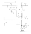
- FIG. 2 is a circuit diagram illustrating a detailed configuration example of a pixel or the like illustrated in FIG. 1.
- FIG. 3 is a cross-sectional view illustrating a configuration of a transistor illustrated in FIG. 2.
- 13 is a TEM (Transmission Electron Microscope) photograph (corresponding to the structure shown in FIG. 12) for explaining the film thickness of a silicon oxide film. It is sectional drawing which represented a part of FIG. 5A typically.
- FIG. 5A typically.
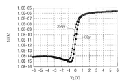
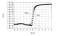
- FIG. 2 is a block diagram illustrating a detailed configuration example of a column selection unit illustrated in FIG. 1. It is a characteristic view for demonstrating the influence on the current-voltage characteristic of the transistor by an X-ray. It is sectional drawing for demonstrating the manufacturing process including the formation process of a semiconductor layer. It is sectional drawing showing the process of following FIG. 7B. It is sectional drawing showing the process of following FIG. 7C. It is sectional drawing showing the process of following FIG. 7D. It is a characteristic view showing the relationship between the sum total of the film thickness of a silicon oxide film, and a threshold voltage shift. 10 is a cross-sectional view illustrating a configuration of a transistor according to Modification 1. FIG.
- FIG. 10 is a cross-sectional view illustrating a configuration of a transistor according to Modification 2.
- FIG. 10 is a cross-sectional view illustrating a configuration of a transistor according to Modification 3-1.
- FIG. 10 is a cross-sectional view illustrating a configuration of a transistor according to Modification 3-2.
- FIG. 10 is a cross-sectional view illustrating a configuration of a transistor according to Modification 3-2.
- FIG. 10 is a circuit diagram illustrating a configuration of a pixel and the like according to Modification 4.
- FIG. 10 is a circuit diagram illustrating a configuration of a pixel and the like according to Modification 5.
- FIG. 16 is a circuit diagram illustrating a configuration of a pixel and the like according to modification 6-1.
- FIG. 16 is a circuit diagram illustrating a configuration of a pixel and the like according to modification example 6-2. It is a schematic diagram showing schematic structure of the imaging display system which concerns on an application example.
- Embodiment an example of a radiation imaging apparatus including a top-gate TFT in which the thickness of a silicon oxide film adjacent to the upper side of the semiconductor layer is larger than that of the silicon oxide film adjacent to the lower side
- Modification 1 (Another example of a top gate transistor) 3.
- Modification 2 (example of bottom gate transistor) 4).
- Modification 3-1 (Example of Dual Gate Transistor) 5.
- Modification 3-2 (Another example of dual gate transistor) 6).
- Modified example 4 an example of another passive pixel circuit) 7).
- Modified example 5 an example of another passive pixel circuit
- Modified examples 6-1 and 6-2 (example of active pixel circuit) 9.
- Application example (example of radiation imaging display system)
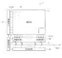
- FIG. 1 illustrates an overall block configuration of a radiation imaging apparatus (radiation imaging apparatus 1) according to an embodiment of the present disclosure.
- the radiation imaging apparatus 1 reads information on a subject (captures a subject) based on, for example, incident radiation Rrad (for example, ⁇ rays, ⁇ rays, ⁇ rays, X rays, etc.).
- the radiation imaging apparatus 1 includes a pixel unit 11, and includes a row scanning unit 13, an A / D conversion unit 14, a column scanning unit 15, and a system control unit 16 as a drive circuit for the pixel unit 11.
- the pixel unit 11 includes a plurality of pixels (imaging pixels, unit pixels) 20 that generate signal charges based on radiation.
- the plurality of pixels 20 are two-dimensionally arranged in a matrix (matrix).
- the horizontal direction (row direction) in the pixel unit 11 will be described as “H” direction and the vertical direction (column direction) will be described as “V” direction.
- the radiation imaging apparatus 1 may be either a so-called indirect conversion type or a direct conversion type as long as it uses a transistor 22 described later as a switching element for reading signal charges from the pixel unit 11.
- 2A shows the configuration of the pixel unit 11 in the case of the indirect conversion type
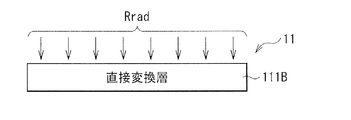
- FIG. 2B shows the configuration of the pixel unit 11 in the case of the direct conversion type.
- the pixel unit 11 has a wavelength conversion layer 112 on the photoelectric conversion layer 111A (light receiving surface side).
- the wavelength conversion layer 112 converts the radiation Rrad into a wavelength in the sensitivity range of the photoelectric conversion layer 111 (for example, visible light).
- This wavelength conversion layer 112 is, for example, a phosphor that converts X-rays into visible light (for example, CsI (added with Tl), Gd 2 O 2 S, BaFX (X is Cl, Br, I, etc.), NaI, CaF 2, etc. Scintillator).
- Such a wavelength conversion layer 112 is formed on the photoelectric conversion layer 111A through a planarization film made of, for example, an organic material or a spin-on-glass material.
- the photoelectric conversion layer 111A includes a photoelectric conversion element (a photoelectric conversion element 21 described later) such as a photodiode.
- the pixel unit 11 has a conversion layer (direct conversion layer 111B) that absorbs incident radiation Rrad and generates an electrical signal (holes and electrons).
- the direct conversion layer 111B is made of, for example, an amorphous selenium (a-Se) semiconductor, a cadmium tellurium (CdTe) semiconductor, or the like.
- the radiation imaging apparatus 1 may be either an indirect conversion type or a direct conversion type.
- the case of the indirect conversion type will be mainly described as an example. . That is, in the pixel unit 11, the radiation Rrad is converted into visible light in the wavelength conversion layer 112, and then the visible light is converted into an electric signal in the photoelectric conversion layer 111A (photoelectric conversion element 21). It is read out as a signal charge.
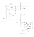
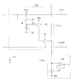
- FIG. 3 illustrates a circuit configuration of the pixel 20 (a so-called passive circuit configuration) together with a circuit configuration of a later-described charge amplifier circuit 171 in the A / D conversion unit 14.
- This passive pixel 20 is provided with one photoelectric conversion element 21 and one transistor 22.
- the pixel 20 is also connected to a read control line Lread extending along the H direction and a signal line Lsig extending along the V direction.
- the photoelectric conversion element 21 includes, for example, a PIN (Positive Intrinsic Negative) type photodiode or a MIS (Metal-Insulator-Semiconductor) type sensor, and generates a signal charge having a charge amount corresponding to the amount of incident light as described above.
- the cathode of the photoelectric conversion element 21 is connected to the storage node N here.
- the transistor 22 is turned on in response to the row scanning signal supplied from the read control line Lread, so that the signal charge (input voltage Vin) obtained by the photoelectric conversion element 21 is output to the signal line Lsig (read).
- Transistor is configured by an N channel type (N type) field effect transistor (FET).
- FET field effect transistor
- the transistor 22 may be composed of a P-channel type (P-type) FET or the like.
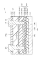
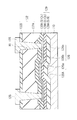
- FIG. 4 shows a cross-sectional structure of the transistor 22.
- the transistor 22 has a so-called top gate type thin film transistor element structure.
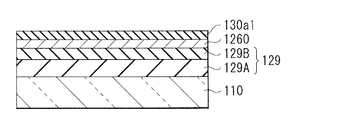
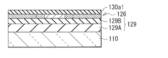
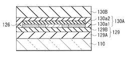
- the transistor 22 includes, for example, a first gate insulating film 129 (first gate insulating film), a semiconductor layer 126, a second gate insulating film 130 (second gate insulating film), and a first gate electrode 120A on a substrate 110. In this order.
- An interlayer insulating film 131 is formed on the first gate electrode 120A, and a contact hole H1 penetrating the interlayer insulating film 131 and the second gate insulating film 130 is formed.
- source / drain electrodes 128 are provided so as to fill the contact holes H1.
- the semiconductor layer 126 includes, for example, a channel layer (active layer) 126a, an LDD (Lightly Doped Drain) layer 126b, and an N + layer 126c.
- amorphous silicon amorphous silicon
- microcrystalline silicon or polycrystalline silicon (polysilicon)
- polysilicon polycrystalline silicon
- LTPS Low Temperature Poly-silicon
- oxide semiconductors such as indium gallium zinc oxide (InGaZnO) or zinc oxide (ZnO).
- the LDD layer 126b is formed between the channel layer 126a and the N + layer 126c for the purpose of reducing leakage current.
- the source / drain electrode 128 functions as a source or drain, and is a single-layer film made of any of titanium (Ti), aluminum (Al), molybdenum (Mo), tungsten (W), chromium (Cr), and the like. Or a laminated film containing two or more of them.
- the first gate electrode 120A is, for example, a single layer film made of any one of molybdenum, titanium, aluminum, tungsten, chromium, or the like, or a laminated film including two or more of them.
- the first gate electrode 120A is provided to face the semiconductor layer 126 (specifically, the channel layer 126a) with the second gate insulating film 130 in between (the semiconductor layer 126 faces the first gate electrode 120A). A region to be the channel layer 126a).
- Each of the first gate insulating film 129 and the second gate insulating film 130 includes a silicon oxide film (a silicon compound film containing oxygen) such as silicon oxide (SiO x ) or silicon oxynitride (SiON). Yes.
- the first gate insulating film 129 and the second gate insulating film 130 are each a single-layer film made of, for example, silicon oxide or silicon oxynitride, or such a silicon oxide film and silicon nitride A laminated film including a silicon nitride film such as a (SiN x ) film.
- the silicon oxide film is provided on the semiconductor layer 126 side (adjacent to the semiconductor layer 126).
- the semiconductor layer 126 is made of, for example, low-temperature polycrystalline silicon, a silicon oxide film is formed adjacent to the semiconductor layer 126 for reasons of the manufacturing process.
- the first gate insulating film 129 and the second gate insulating film 130 are each preferably a laminated film including the silicon oxide film and the silicon nitride film.
- the first gate insulating film 129 and the second gate insulating film 130 are each a laminated film.
- the first gate insulating film 129 is formed by laminating, for example, a silicon nitride film 129A and a silicon oxide film 129B sequentially from the substrate 110 side.
- the second gate insulating film 130 is formed by stacking, for example, a silicon oxide film 130A, a silicon nitride film 130B, and a silicon oxide film 130C in this order from the semiconductor layer 126 side.
- the silicon oxide film 129B of this embodiment corresponds to a specific example of the “first silicon oxide film” of the present disclosure
- the silicon oxide film 130A corresponds to the “second silicon oxide film” of the present disclosure. This corresponds to a specific example.
- the thickness of the silicon oxide film 130A of the second gate insulating film 130 adjacent to the upper side (upper surface) of the semiconductor layer 126 is equal to the first gate insulating film 129 adjacent to the lower side (lower surface) of the semiconductor layer 126. This is equal to or higher than that of the silicon oxide film 129B. Further, the total thickness of the silicon oxide film 129B and the silicon oxide film 130A is desirably, for example, 65 nm or less. This is because the shift of the threshold voltage of the transistor 22 to the negative side can be reduced to suppress the characteristic deterioration.
- each thickness of the first gate insulating film 129 and the second gate insulating film 130 is, for example, in the first gate insulating film 129, the thickness of the silicon nitride film 129A is, for example, 30 nm to 120 nm, and the silicon oxide film The thickness of 129B is, for example, 5 nm to 60 nm.
- the thickness of the silicon oxide film 130A is, for example, 5 nm to 60 nm
- the thickness of the silicon nitride film 130B is, for example, 10 nm to 120 nm
- the thickness of the silicon oxide film 130C is, for example, 5 nm to 60 nm.
- the thicknesses of the silicon oxide films 129B and 130A are set so as to satisfy the above magnitude relationship, and preferably the total thickness is set to 65 nm or less.
- the capacitance (gate capacitance) between the semiconductor layer 126 and the first gate electrode 120A is determined according to the dielectric constant, thickness, and the like of each film constituting the second gate insulating film 130.
- the silicon oxide films 129B and 130A are adjacent to the semiconductor layer 126 for reasons of the manufacturing process. From the viewpoint of transistor characteristics (details will be described later), the silicon oxide films 129B and 130A It is desirable that the total thickness is relatively thin (for example, 65 nm or less). Therefore, in the second gate insulating film 130, the gate capacitance can be set by mainly adjusting the thickness of the silicon nitride film 130B in the stacked structure.
- the thickness of the silicon nitride film 130B is desirably larger than the thickness of the silicon oxide film 130A, for example, 10 nm or more. This makes it easier to form a desired gate capacitance while maintaining the total thickness of the silicon oxide film 129A and the silicon oxide film 130B at, for example, 65 nm or less.
- each film (particularly the silicon oxide film 130A) in the second gate insulating film 130 is desirably measured at a specific site as follows, for example. That is, as shown in FIG. 5A, in the stacked structure of the transistor 22, a minute protrusion X is likely to be generated on the surface of the semiconductor layer 126 (channel layer 126a) made of, for example, polycrystalline silicon. As a result, in each film above the semiconductor layer 126, particularly the silicon oxide film 130A, it is difficult to obtain good coverage in the vicinity of the protrusion X (it is likely to become thin locally). Therefore, as schematically shown in FIG. 5B, it is desirable to use the thickness (t) in the flat portion A between the protrusions X as the thickness of at least the silicon oxide film 130A of the second gate insulating film 130.
- the interlayer insulating film 131 is, for example, a single layer film made of any one of silicon oxide, silicon oxynitride, and silicon nitride, or a laminated film including two or more of them.
- the interlayer insulating film 131 is formed by laminating a silicon oxide film 131A, a silicon nitride film 131B, and a silicon oxide film 131C in this order from the first gate electrode 120A side.
- another interlayer insulating film may be formed so as to cover the interlayer insulating film 131 and the source / drain electrode 128.
- the row scanning unit 13 includes a shift register circuit, a predetermined logic circuit, and the like, which will be described later, and drives (line-sequentially) a plurality of pixels 20 in the pixel unit 11 in units of rows (horizontal line units).
- This is a pixel driver (row scanning circuit) that performs scanning. Specifically, an imaging operation such as a read operation or a reset operation of each pixel 20 is performed by, for example, line sequential scanning. Note that this line sequential scanning is performed by supplying the above-described row scanning signal to each pixel 20 via the readout control line Lread.
- the A / D conversion unit 14 has a plurality of column selection units 17 provided for each of a plurality (here, four) of signal lines Lsig, and the signal voltage (via the signal line Lsig ( A / D conversion (analog / digital conversion) is performed based on the voltage according to the signal charge. Thereby, output data Dout (imaging signal) composed of a digital signal is generated and output to the outside.
- each column selection unit 17 includes a charge amplifier 172, a capacitive element (capacitor or feedback capacitive element) C1, a switch SW1, a sample hold (S / H) circuit 173, and four switches SW2.
- a multiplexer circuit (selection circuit) 174 including the A / D converter 175 is included.
- the charge amplifier 172, the capacitor C1, the switch SW1, the S / H circuit 173, and the switch SW2 are provided for each signal line Lsig.
- the multiplexer circuit 174 and the A / D converter 175 are provided for each column selection unit 17.
- the charge amplifier 172, the capacitive element C1, and the switch SW1 constitute the charge amplifier circuit 171 shown in FIG.
- the charge amplifier 172 is an amplifier (amplifier) for converting the signal charge read from the signal line Lsig into a voltage (QV conversion).
- one end of the signal line Lsig is connected to the negative ( ⁇ ) input terminal, and a predetermined reset voltage Vrst is input to the positive (+) input terminal.
- the output terminal of the charge amplifier 172 and the negative input terminal are connected in a feedback manner (feedback connection) via a parallel connection circuit of the capacitive element C1 and the switch SW1. That is, one terminal of the capacitive element C1 is connected to the negative input terminal of the charge amplifier 172, and the other terminal is connected to the output terminal of the charge amplifier 172.
- one terminal of the switch SW1 is connected to the negative input terminal of the charge amplifier 172, and the other terminal is connected to the output terminal of the charge amplifier 172.
- the on / off state of the switch SW1 is controlled by a control signal (amplifier reset control signal) supplied from the system control unit 16 via the amplifier reset control line Lcarst.
- the S / H circuit 173 is disposed between the charge amplifier 172 and the multiplexer circuit 174 (switch SW2), and is a circuit for temporarily holding the output voltage Vca from the charge amplifier 172.
- the multiplexer circuit 174 selectively connects each S / H circuit 173 and the A / D converter 175 by sequentially turning on one of the four switches SW2 in accordance with the scanning drive by the column scanning unit 15. Or it is a circuit to cut off.
- the A / D converter 175 is a circuit that generates and outputs the output data Dout by performing A / D conversion on the output voltage from the S / H circuit 173 input through the switch SW2. .
- the column scanning unit 15 includes, for example, a shift register and an address decoder (not shown), and drives the switches SW2 in the column selection unit 17 in order while scanning.
- the signal (the output data Dout) of each pixel 20 read through each of the signal lines Lsig is sequentially output to the outside.
- the system control unit 16 controls the operations of the row scanning unit 13, the A / D conversion unit 14, and the column scanning unit 15. Specifically, the system control unit 16 includes a timing generator that generates the various timing signals (control signals) described above, and the row scanning unit based on the various timing signals generated by the timing generator. 13. Drive control of the A / D conversion unit 14 and the column scanning unit 15 is performed. Based on the control of the system control unit 16, the row scanning unit 13, the A / D conversion unit 14, and the column scanning unit 15 perform imaging driving (line sequential imaging driving) for each of the plurality of pixels 20 in the pixel unit 11. Thus, the output data Dout is acquired from the pixel unit 11.
- imaging driving line sequential imaging driving
- the signal charges read in this way are input to the column selection unit 17 in the A / D conversion unit 14 for each of a plurality (here, four) of pixel columns via the signal line Lsig.
- the column selection unit 17 first performs QV conversion (conversion from signal charge to signal voltage) in a charge amplifier circuit including a charge amplifier 172 and the like for each signal charge input from each signal line Lsig.
- QV conversion conversion from signal charge to signal voltage
- a / D conversion is performed in the A / D converter 175 via the S / H circuit 173 and the multiplexer circuit 174 for each converted signal voltage (output voltage Vca from the charge amplifier 172), and an output consisting of a digital signal is performed.
- Data Dout imaging signal
- the output data Dout is sequentially output from each column selection unit 17 and transmitted to the outside (or input to an internal memory not shown).
- the transistor 22 includes silicon oxide films (silicon oxide films 129B and 130A) in the first gate insulating film 129 and the second gate insulating film 130.
- silicon oxide films silicon oxide films 129B and 130A
- electrons in the films are excited by the so-called photoelectric effect, Compton scattering, or electron pair generation.
- the threshold voltage Vth of the transistor 22 is shifted to the negative side (minus side), the S (threshold) value is deteriorated, and the like, which causes an increase in off current or a decrease in on current.
- FIG. 7A shows the relationship (current-voltage characteristics) of the drain current (current between the source and drain) Id with respect to the gate voltage Vg of the transistor 22 for each X-ray irradiation dose.
- Irradiation conditions are a tube voltage of 80 kV, a dose rate of 3.2 mGy / sec, and the irradiation dose is 0 Gy (initial value), 54 Gy, 79 Gy, 104 Gy, 129 Gy, 154 Gy, 254 Gy, and 354 Gy.
- low-temperature polycrystalline silicon is used for the semiconductor layer 126, and the voltage Vds between the source and the drain is 0.1V.
- the surface of the semiconductor layer 126 is likely to be rough (protrusions X are easily generated), and the silicon oxide film 130A is likely to be locally thin.
- the thickness of the silicon oxide film 130A of the second gate insulating film 130 is equal to or greater than the thickness of the silicon oxide film 129B of the first gate insulating film 129. Coverage is obtained, and transistor characteristics (threshold voltage characteristics or S value) are improved. In addition, variations in the characteristics of each element can be suppressed.
- stopper film 130a1 made of, for example, silicon oxide (SiO 2 ) is used.
- SiO 2 silicon oxide
- the stopper film 130a1 is formed on the polysilicon layer 1260. To do. Subsequently, as shown in FIG. 7C, the polysilicon layer 1260 is doped with impurities through the stopper film 130a1 to form the semiconductor layer 126. In this manner, by using the stopper film 130a1 when the semiconductor layer 126 is formed, the process can be performed without exposing (not exposing) the interface of the semiconductor layer 126 (particularly, the channel layer 126a).
- the semiconductor layer 126 and the stopper film 130a1 are patterned into a predetermined shape.
- the end face of the semiconductor layer 126 (side face of the N + layer 126c) is exposed.
- the silicon nitride film 130B is formed in this state, the threshold voltage shifts to the negative side due to the influence of the interface state. It becomes easy to do. Therefore, as shown in FIG. 7E, another layer of silicon oxide film 130a2 is formed so as to cover the end face of the semiconductor layer 126 and the stopper film 130a1.
- deterioration of the transistor characteristics can be suppressed when the thickness of the upper silicon oxide film 130A is equal to or greater than the thickness of the lower silicon oxide film 129B of the semiconductor layer 126.
- the characteristics of the transistor 22 are improved. This is particularly effective when the total thickness of the silicon oxide films 129B and 130A adjacent to the semiconductor layer 126 is set to 65 nm or less (thinned) as will be described later.
- the characteristic deterioration due to the hole trap as described above can also be suppressed, and the reliability can be further improved.
- FIG. 7F shows the relationship between the total thickness (total thickness) of the silicon oxide (SiO 2 ) film and the threshold voltage shift amount ( ⁇ Vth).
- the sign of ⁇ (minus) on the vertical axis indicates that the threshold voltage is shifted to the negative side.
- the thickness of the silicon oxide film and the threshold voltage there is a correlation between the thickness of the silicon oxide film and the threshold voltage, and it has linearity. For example, when the total thickness of the silicon oxide films 129B and 130A is 65 nm or less, the shift amount can be maintained at 2 V or less, and a sufficient transistor life can be ensured.
- the transistor 22 for reading out signal charges based on the radiation Rrad from each pixel 20 includes the silicon oxide film 129B, the semiconductor layer 126, the silicon oxide film 130A, and the first electrode in order from the substrate 110 side. And an element structure including a gate electrode. Since the thickness of the silicon oxide film 130A is equal to or greater than the thickness of the silicon oxide film 129B, the manufacturing yield of the transistor 22 is improved. Therefore, a highly reliable element structure can be realized.
- FIG. 8 illustrates a cross-sectional configuration of a transistor according to the first modification.
- the second gate insulating film (second gate insulating film 130) is formed by sequentially forming the silicon oxide film 130A, the silicon nitride film 130B, and the silicon oxide film 130C from the semiconductor layer 126 side.
- the stacked three-layer structure is used, the stacked structure of the second gate insulating film is not limited to this.
- a two-layer structure in which a silicon oxide film 134A and a silicon nitride film 134B are stacked in this order from the semiconductor layer 126 side as in the second gate insulating film (second gate insulating film 134). May be.
- FIG. 9A shows current-voltage characteristics before and after X-ray irradiation of the transistor 22 (referred to as Example 1) in the above embodiment
- FIG. 9B shows before and after X-ray irradiation of the transistor according to this modification (referred to as Example 2). It represents current-voltage characteristics.
- the X-ray irradiation conditions are the same as those in the case of FIG.
- FIG. 10 shows the threshold voltage shift amount ( ⁇ Vth) after X-ray irradiation (25 Gy) in the current-voltage characteristics of Examples 1 and 2.
- the threshold voltage Vth the gate voltage in the case where the current Id is 1.0 ⁇ 10 ⁇ 13 (A) is used.
- the current-voltage characteristics in the element structure of this modification are the same as those in the above embodiment, and the behavior by X-ray irradiation is also the same. Therefore, also in this modification, the same effect as the above-described embodiment can be obtained.
- the second gate insulating film 130 may have a three-layer structure. It may be a layered structure.
- the second gate insulating film 130 may be composed of, for example, a single layer film of a silicon oxide film 130A.
- FIG. 11 illustrates a cross-sectional configuration of a transistor according to the second modification.
- a top-gate element structure is illustrated, but the transistor of the present disclosure may have a so-called bottom-gate element structure as in the present modification.
- the element structure of this modification includes, for example, a first gate electrode 120A, a first gate insulating film 129, a semiconductor layer 126, and a silicon oxide film 130A in order from the substrate 110 side.
- an interlayer insulating film 132 is formed on the silicon oxide film 130A, and a contact hole H1 penetrating the interlayer insulating film 132 and the silicon oxide film 130A is formed.
- the interlayer insulating film 132 is a stacked film including, for example, a silicon nitride film 132A and a silicon oxide film 132B in this order from the silicon oxide film 130A side.
- the thickness of the silicon oxide film 130A is equal to or greater than the thickness of the silicon oxide film 129B, an effect equivalent to that of the above embodiment can be obtained.
- the thickness of the silicon nitride film 132A of the interlayer insulating film 132 is desirably larger than the thickness of the silicon oxide film 130A (for example, 10 nm or more).
- the total thickness of the silicon oxide films 129B and 130a adjacent to the semiconductor layer 126 is desirably 65 nm or less.
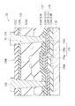
- FIG. 12 illustrates a cross-sectional configuration of a transistor according to Modification 3-1.
- the top gate type element structure is illustrated, but the transistor of the present disclosure may have a so-called dual gate type element structure as in the present modification.
- the element structure of this modification has, for example, a first gate electrode 120A, a first gate insulating film 129, a semiconductor layer 126, a second gate insulating film 130, and a second gate electrode 120B in this order from the substrate 110 side.
- An interlayer insulating film 133 is formed on the second gate insulating film 130 and the second gate electrode 120B, and a contact hole H1 penetrating the interlayer insulating film 133 and the second gate insulating film 130 is formed. ing. On the interlayer insulating film 133, source / drain electrodes 128 are provided so as to fill the contact holes H1.
- the interlayer insulating film 133 is a stacked film including, for example, a silicon oxide film 133A, a silicon nitride film 133B, and a silicon oxide film 133C in this order from the silicon oxide film 130A side.
- the thickness of the silicon oxide film 130A is equal to or greater than the thickness of the silicon oxide film 129B, an effect equivalent to that of the above embodiment can be obtained.
- the thickness of the silicon nitride film 132A of the interlayer insulating film 132 is larger than the thickness of the silicon oxide film 130A (for example, 10 nm or more).
- the total thickness of the silicon oxide films 129B and 130a adjacent to the semiconductor layer 126 is desirably 65 nm or less.
- FIG. 13 illustrates a cross-sectional configuration of a transistor according to Modification 3-2.
- the laminated structure of the second gate insulating film is not particularly limited, and the second-layered second gate insulating film 134 described in the modified example 1 is used. May be.
- FIG. 14 illustrates a circuit configuration of a pixel (pixel 20A) according to Modification 4 together with the circuit configuration example of the charge amplifier circuit 171 described in the above embodiment.
- the pixel 20 ⁇ / b> A of this modification has a so-called passive circuit configuration, and includes one photoelectric conversion element 21 and one transistor 22.
- the pixel 20A is connected to a read control line Lread extending along the H direction and a signal line Lsig extending along the V direction.
- the anode of the photoelectric conversion element 21 is connected to the storage node N, and the cathode is connected to the ground (ground).
- the storage node N may be connected to the anode of the photoelectric conversion element 21 in the pixel 20A, and even in such a configuration, the same as the radiation imaging apparatus 1 of the above embodiment. An effect can be obtained.
- FIG. 15 illustrates a circuit configuration of a pixel (pixel 20B) according to Modification 5 together with the circuit configuration example of the charge amplifier circuit 171 described in the above embodiment.
- the pixel 20B according to the present modification has a so-called passive circuit configuration, includes one photoelectric conversion element 21, and a read control line Lread extending in the H direction. , And a signal line Lsig extending along the V direction.
- the pixel 20 ⁇ / b> B has two transistors 22. These two transistors 22 are connected to each other in series (one source or drain and the other source or drain are electrically connected. In this way, two transistors 22 are provided in one pixel 20B. Thus, off-leakage can be reduced.
- two transistors 22 connected in series may be provided in the pixel 20B, and in this case as well, the same effect as in the above embodiment can be obtained.
- Three or more transistors may be connected in series.
- FIG. 16 illustrates a circuit configuration of a pixel (pixel 20C) according to Modification 6-1 along with a circuit configuration example of a charge amplifier circuit 171A described below.
- FIG. 17 shows the circuit configuration of the pixel (pixel 20D) according to the modification 6-2 together with the circuit configuration example of the charge amplifier circuit 171A.
- the pixels 20 C and 20 D according to these modified examples 6-1 and 6-2 have so-called active pixel circuits.
- the active pixels 20C and 20D are provided with one photoelectric conversion element 21 and three transistors 22, 23, and 24.
- a read control line Lread and a reset control line Lrst extending along the H direction and a signal line Lsig extending along the V direction are also connected to the pixels 20C and 20D.
- the gate of the transistor 22 is connected to the read control line Lread, the source is connected to the signal line Lsig, and the drain is connected to the drain of the transistor 23 constituting the source follower circuit.
- the source of the transistor 23 is connected to the power supply VDD, the gate is connected to the cathode (example in FIG. 16) or the anode (example in FIG. 17) of the photoelectric conversion element 21 via the storage node N, and the transistor functions as a reset transistor. 24 drains.
- the gate of the transistor 24 is connected to the reset control line Lrst, and the reset voltage Vrst is applied to the source.
- the anode of the photoelectric conversion element 21 is connected to the ground
- Modification Example 6-2 the cathode of the photoelectric conversion element 21 is connected to the ground.
- the charge amplifier circuit 171A is provided with an amplifier 176 and a constant current source 177 instead of the charge amplifier 172, the capacitive element C1, and the switch SW1 in the charge amplifier circuit 171 described above. It is a thing.
- the signal line Lsig is connected to the positive input terminal, and the negative input terminal and the output terminal are connected to each other to form a voltage follower circuit.
- one terminal of the constant current source 177 is connected to one end side of the signal line Lsig, and the power source VSS is connected to the other terminal of the constant current source 177.
- the indirect conversion type or direct conversion type radiation imaging apparatus as described above is used as various types of radiation imaging apparatuses that obtain an electrical signal based on the radiation Rrad.
- medical X-ray imaging devices Digital Radiography, etc.
- X-ray imaging devices for portable object inspection used at airports, etc. X-ray imaging devices for portable object inspection used at airports, etc.
- industrial X-ray imaging devices for example, devices for inspecting dangerous goods in containers, etc.
- FIG. 18 schematically illustrates a schematic configuration example of a radiation imaging display system (radiation imaging display system 5) according to an application example.
- the radiation imaging display system 5 includes a radiation imaging apparatus 1 including the pixel unit 11 and the like according to the above-described embodiment, an image processing unit 52, and a display device 4, and in this example, radiation imaging using radiation It is a display system.
- the image processing unit 52 generates image data D1 by performing predetermined image processing on the output data Dout (imaging signal) output from the radiation imaging apparatus 1.
- the display device 4 performs image display on the predetermined monitor screen 40 based on the image data D ⁇ b> 1 generated by the image processing unit 52.
- the radiation imaging apparatus 1 acquires image data Dout of the subject 50 based on the radiation Rrad emitted toward the subject 50 from the radiation source 51 such as an X-ray source, and the image processing unit 52. Output to.
- the image processing unit 52 performs the predetermined image processing described above on the input image data Dout, and outputs the image data (display data) D1 after the image processing to the display device 4.
- the display device 4 displays image information (captured image) on the monitor screen 40 based on the input image data D1.
- the image of the subject 50 can be acquired as an electrical signal in the radiation imaging apparatus 1, image display is performed by transmitting the acquired electrical signal to the display device 4. It can be carried out. That is, it is possible to observe the image of the subject 50 without using a photographic film, and it is also possible to handle moving image shooting and moving image display.
- the first and second gate insulating films are illustrated by laminating one to three insulating films, but the first and second gate insulating films include four or more insulating films. It may be a laminate of films. In any stacked structure, a silicon oxide film is provided on the semiconductor layer side of the second gate insulating film, and this silicon oxide film is equal to or greater than the thickness of the silicon oxide film in the first gate insulating film. If it is formed with the thickness, the effect of the present disclosure can be obtained.
- circuit configuration of the pixel in the pixel portion of the above-described embodiment and the like is not limited to that described in the above-described embodiment (circuit configuration of the pixels 20, 20A to 20D), and other circuit configurations may be used. Good.
- circuit configurations of the row scanning unit, the column selection unit, and the like are not limited to those described in the above embodiments and the like, and other circuit configurations may be used.
- the pixel unit, the row scanning unit, the A / D conversion unit (column selection unit), the column scanning unit, and the like described in the above embodiments may be formed on the same substrate, for example.
- a polycrystalline semiconductor such as low-temperature polycrystalline silicon
- switches and the like in these circuit portions can be formed on the same substrate. For this reason, for example, it becomes possible to perform a driving operation on the same substrate based on a control signal from an external system control unit, and to improve reliability when narrowing the frame (three-side free frame structure) or wiring connection. Can be realized.
- this indication can also take the following structures.
- a plurality of pixels generating signal charges based on radiation;
- a field effect transistor for reading out the signal charge from the plurality of pixels, The transistor is A first silicon oxide film, a semiconductor layer including an active layer, and a second silicon oxide film, which are sequentially stacked from the substrate side;
- a first gate electrode disposed opposite to the semiconductor layer with the first or second silicon oxide film in between, The thickness of the second silicon oxide film is equal to or greater than the thickness of the first silicon oxide film.
- the radiation imaging apparatus according to (6) wherein a silicon nitride film having a thickness larger than that of the second silicon oxide film is provided on the second silicon oxide film.
- the thickness of the silicon nitride film is 10 nm or more.
- the transistor includes, in order from the substrate side, the first gate electrode, the first silicon oxide film, the semiconductor layer, and the second silicon oxide film, and the second silicon oxide film
- the radiation imaging apparatus according to (1) further including a second gate electrode facing the first gate electrode.
- the semiconductor layer includes low-temperature polycrystalline silicon.
- Each of the plurality of pixels has a photoelectric conversion element;
- the radiation imaging apparatus 15) The radiation imaging apparatus according to (14), wherein the photoelectric conversion element includes a PIN type photodiode or a MIS type sensor. (16) The radiation imaging apparatus according to any one of (1) to (13), wherein each of the plurality of pixels includes a conversion layer that absorbs the radiation and generates the signal charge. (17) The radiation imaging apparatus according to any one of (1) to (16), wherein the radiation is X-rays.
- the radiation imaging apparatus includes: A plurality of pixels generating signal charges based on radiation; A field effect transistor for reading out the signal charge from the plurality of pixels, The transistor is A first silicon oxide film, a semiconductor layer including an active layer, and a second silicon oxide film, which are sequentially stacked from the substrate side; A first gate electrode disposed opposite to the semiconductor layer with the first or second silicon oxide film in between, The radiation imaging display system, wherein the thickness of the second silicon oxide film is equal to or greater than the thickness of the first silicon oxide film.
Abstract
Description
1.実施の形態(半導体層の上側に隣接するシリコン酸化物膜の厚みを、下側に隣接するシリコン酸化物膜よりも大きくしたトップゲート型TFTを含む放射線撮像装置の例)
2.変形例1(トップゲート型トランジスタの他の例)
3.変形例2(ボトムゲート型トランジスタの例)
4.変形例3-1(デュアルゲート型トランジスタの例)
5.変形例3-2(デュアルゲート型トランジスタの他の例)
6.変形例4(パッシブ型の他の画素回路の例)
7.変形例5(パッシブ型の他の画素回路の例)
8.変形例6-1,6-2(アクティブ型の画素回路の例)
9.適用例(放射線撮像表示システムの例) Hereinafter, embodiments of the present disclosure will be described in detail with reference to the drawings. The description will be given in the following order.
1. Embodiment (an example of a radiation imaging apparatus including a top-gate TFT in which the thickness of a silicon oxide film adjacent to the upper side of the semiconductor layer is larger than that of the silicon oxide film adjacent to the lower side)
2. Modification 1 (Another example of a top gate transistor)
3. Modification 2 (example of bottom gate transistor)
4). Modification 3-1 (Example of Dual Gate Transistor)
5. Modification 3-2 (Another example of dual gate transistor)
6). Modified example 4 (an example of another passive pixel circuit)
7). Modified example 5 (an example of another passive pixel circuit)
8). Modified examples 6-1 and 6-2 (example of active pixel circuit)
9. Application example (example of radiation imaging display system)
[構成]
図1は、本開示の一実施の形態に係る放射線撮像装置(放射線撮像装置1)の全体のブロック構成を表すものである。放射線撮像装置1は、例えば入射する放射線Rrad(例えばα線,β線,γ線,X線等)に基づいて被写体の情報を読み取る(被写体を撮像する)ものである。この放射線撮像装置1は、画素部11を備えると共に、この画素部11の駆動回路として、行走査部13、A/D変換部14、列走査部15およびシステム制御部16を備えている。 <Embodiment>
[Constitution]
FIG. 1 illustrates an overall block configuration of a radiation imaging apparatus (radiation imaging apparatus 1) according to an embodiment of the present disclosure. The
画素部11は、放射線に基づいて信号電荷を発生させる複数の画素(撮像画素,単位画素)20を備えたものである。複数の画素20は、行列状(マトリクス状)に2次元配置されている。尚、図1中に示したように、以下、画素部11内における水平方向(行方向)を「H」方向とし、垂直方向(列方向)を「V」方向として説明する。放射線撮像装置1は、この画素部11からの信号電荷の読み出しのためのスイッチング素子として後述のトランジスタ22を用いるものであれば、いわゆる間接変換型および直接変換型のいずれのタイプであってもよい。図2Aに、間接変換型の場合の画素部11の構成、図2Bに、直接変換型の場合の画素部11の構成をそれぞれ示す。 (Pixel part 11)
The
第1ゲート絶縁膜129および第2ゲート絶縁膜130はそれぞれ、例えば酸化シリコン(SiOx)または酸窒化シリコン(SiON)等のシリコン酸化物膜(酸素を含むシリコン化合物膜)を含んで構成されている。具体的には、第1ゲート絶縁膜129および第2ゲート絶縁膜130はそれぞれ、例えば酸化シリコンまたは酸窒化シリコン等からなる単層膜であるか、あるいはこのようなシリコン酸化物膜と、窒化シリコン(SiNx)膜等のシリコン窒化物膜とを含む積層膜である。これらの第1ゲート絶縁膜129および第2ゲート絶縁膜130のいずれにおいても、上記シリコン酸化物膜が、半導体層126側に(半導体層126に隣接して)設けられている。半導体層126が例えば低温多結晶シリコンからなる場合には、製造プロセス上の理由から、半導体層126に隣接して、シリコン酸化物膜が形成される。 (Configuration of gate insulating film)
Each of the first
行走査部13は、後述のシフトレジスタ回路や所定の論理回路等を含んで構成されており、画素部11内の複数の画素20に対して行単位(水平ライン単位)での駆動(線順次走査)を行う画素駆動部(行走査回路)である。具体的には、各画素20の読み出し動作やリセット動作等の撮像動作を例えば線順次走査により行う。尚、この線順次走査は、読み出し制御線Lreadを介して前述した行走査信号を各画素20へ供給することによって行われる。 (Row scanning unit 13)
The
A/D変換部14は、複数(ここでは4つ)の信号線Lsigごとに1つ設けられた複数の列選択部17を有しており、信号線Lsigを介して入力された信号電圧(信号電荷に応じた電圧)に基づいてA/D変換(アナログ/デジタル変換)を行うものである。これにより、デジタル信号からなる出力データDout(撮像信号)が生成され、外部へ出力される。 (A / D converter 14)
The A /
出力する回路である。 The A /
列走査部15は、例えば図示しないシフトレジスタやアドレスデコーダ等を含んで構成されており、上記した列選択部17内の各スイッチSW2を走査しつつ順番に駆動するものである。このような列走査部15による選択走査によって、信号線Lsigの各々を介して読み出された各画素20の信号(上記出力データDout)が、順番に外部へ出力されるようになっている。 (Column scanning unit 15)
The
システム制御部16は、行走査部13、A/D変換部14および列走査部15の各動作を制御するものである。具体的には、システム制御部16は、前述した各種のタイミング信号(制御信号)を生成するタイミングジェネレータを有しており、このタイミングジェネレータにおいて生成される各種のタイミング信号を基に、行走査部13、A/D変換部14および列走査部15の駆動制御を行う。このシステム制御部16の制御に基づいて、行走査部13、A/D変換部14および列走査部15がそれぞれ画素部11内の複数の画素20に対する撮像駆動(線順次撮像駆動)を行うことにより、画素部11から出力データDoutが取得されるようになっている。 (System control unit 16)
The
本実施の形態の放射線撮像装置1では、例えばX線などの放射線Rradが画素部11へ入射すると、各画素20(ここでは、光電変換素子21)において、入射光に基づく信号電荷が発生する。このとき、詳細には、図3に示した蓄積ノードNにおいて、発生した信号電荷の蓄積により、ノード容量に応じた電圧変化が生じる。これにより、トランジスタ22のドレインには入力電圧Vin(信号電荷に対応した電圧)が供給される。この後、読み出し制御線Lreadから供給される行走査信号に応じてトランジスタ22がオン状態になると、上記した信号電荷が信号線Lsigへ読み出される。 [Action, effect]
In the
図8は、変形例1に係るトランジスタの断面構成を表したものである。上記実施の形態(図3の例)では、第2ゲート絶縁膜(第2ゲート絶縁膜130)を、半導体層126の側から順に、酸化シリコン膜130A、窒化シリコン膜130Bおよび酸化シリコン膜130Cを積層した3層構造としたが、第2ゲート絶縁膜の積層構造はこれに限定されるものではない。例えば、本変形例のように、第2ゲート絶縁膜(第2ゲート絶縁膜134)のように、半導体層126の側から順に酸化シリコン膜134Aおよび窒化シリコン膜134Bを積層した2層構造であってもよい。 <
FIG. 8 illustrates a cross-sectional configuration of a transistor according to the first modification. In the above embodiment (example in FIG. 3), the second gate insulating film (second gate insulating film 130) is formed by sequentially forming the
図11は、変形例2に係るトランジスタの断面構成を表したものである。上記実施の形態では、トップゲート型の素子構造を例示したが、本開示のトランジスタは、本変形例のようにいわゆるボトムゲート型の素子構造であってもよい。本変形例の素子構造は、例えば基板110側から順に、第1ゲート電極120A、第1ゲート絶縁膜129、半導体層126および酸化シリコン膜130Aを有している。また、酸化シリコン膜130A上には、層間絶縁膜132が形成されており、この層間絶縁膜132と、酸化シリコン膜130Aとを貫通するコンタクトホールH1が形成されている。層間絶縁膜132上には、コンタクトホールH1を埋め込むようにソース・ドレイン電極128が設けられている。層間絶縁膜132は、酸化シリコン膜130Aの側から順に、例えば窒化シリコン膜132Aおよび酸化シリコン膜132Bを有する積層膜である。 <
FIG. 11 illustrates a cross-sectional configuration of a transistor according to the second modification. In the above-described embodiment, a top-gate element structure is illustrated, but the transistor of the present disclosure may have a so-called bottom-gate element structure as in the present modification. The element structure of this modification includes, for example, a
図12は、変形例3-1に係るトランジスタの断面構成を表したものである。上記実施の形態では、トップゲート型の素子構造を例示したが、本開示のトランジスタは、本変形例のようにいわゆるデュアルゲート型の素子構造であってもよい。本変形例の素子構造は、例えば基板110側から順に、第1ゲート電極120A、第1ゲート絶縁膜129、半導体層126、第2ゲート絶縁膜130および第2ゲート電極120Bを有している。また、第2ゲート絶縁膜130および第2ゲート電極120B上には、層間絶縁膜133が形成されており、この層間絶縁膜133と第2ゲート絶縁膜130とを貫通するコンタクトホールH1が形成されている。層間絶縁膜133上には、コンタクトホールH1を埋め込むようにソース・ドレイン電極128が設けられている。層間絶縁膜133は、酸化シリコン膜130Aの側から順に、例えば酸化シリコン膜133A、窒化シリコン膜133Bおよび酸化シリコン膜133Cを有する積層膜である。 <Modification 3-1>
FIG. 12 illustrates a cross-sectional configuration of a transistor according to Modification 3-1. In the above embodiment, the top gate type element structure is illustrated, but the transistor of the present disclosure may have a so-called dual gate type element structure as in the present modification. The element structure of this modification has, for example, a
図13は、変形例3-2に係るトランジスタの断面構成を表したものである。上記変形例3-1のデュアルゲート型の素子構造においても、第2ゲート絶縁膜の積層構造は特に限定されず、上記変形例1において説明した2層構造の第2ゲート絶縁膜134が用いられてもよい。 <Modification 3-2>
FIG. 13 illustrates a cross-sectional configuration of a transistor according to Modification 3-2. Also in the dual gate type element structure of the modified example 3-1, the laminated structure of the second gate insulating film is not particularly limited, and the second-layered second
図14は、変形例4に係る画素(画素20A)の回路構成を、上記実施の形態で説明したチャージアンプ回路171の回路構成例と共に表したものである。本変形例の画素20Aは、実施の形態の画素20と同様にいわゆるパッシブ型の回路構成となっており、1つの光電変換素子21と1つのトランジスタ22とを有している。また、この画素20AにはH方向に沿って延在する読み出し制御線Lreadと、V方向に沿って延在する信号線Lsigとが接続されている。 <
FIG. 14 illustrates a circuit configuration of a pixel (
図15は、変形例5に係る画素(画素20B)の回路構成を、上記実施の形態で説明したチャージアンプ回路171の回路構成例と共に表したものである。本変形例の画素20Bは、実施の形態の画素20と同様にいわゆるパッシブ型の回路構成を有し、1つの光電変換素子21を有すると共に、H方向に沿って延在する読み出し制御線Lreadと、V方向に沿って延在する信号線Lsigとに接続されている。 <
FIG. 15 illustrates a circuit configuration of a pixel (
図16は、変形例6-1に係る画素(画素20C)の回路構成を、以下説明するチャージアンプ回路171Aの回路構成例とともに表したものである。また、図17は、変形例6-2に係る画素(画素20D)の回路構成を、チャージアンプ回路171Aの回路構成例とともに表したものである。これらの変形例6-1,6-2に係る画素20C,20Dはそれぞれ、これまで説明した画素20,20A,20Bとは異なり、いわゆるアクティブ型の画素回路を有している。 <Modifications 6-1 and 6-2>
FIG. 16 illustrates a circuit configuration of a pixel (pixel 20C) according to Modification 6-1 along with a circuit configuration example of a
続いて、上記実施の形態および変形例に係る放射線撮像装置は、以下に説明するような放射線撮像表示システムへ適用することも可能である。 <Application example>
Subsequently, the radiation imaging apparatus according to the above-described embodiments and modifications can be applied to a radiation imaging display system as described below.
(1)
放射線に基づく信号電荷を発生する複数の画素と、
前記複数の画素から前記信号電荷を読み出すための電界効果型のトランジスタとを備え、
前記トランジスタは、
基板側から順に積層された、第1のシリコン酸化物膜、活性層を含む半導体層および第2のシリコン酸化物膜と、
前記第1または第2のシリコン酸化膜を間にして前記半導体層に対向配置された第1ゲート電極とを有し、
前記第2のシリコン酸化物膜の厚みは、前記第1のシリコン酸化物膜の厚みと同等以上である
放射線撮像装置。
(2)
前記トランジスタは、前記基板側から順に、前記第1のシリコン酸化物膜、前記半導体層、前記第2のシリコン酸化物膜および前記第1ゲート電極を有する
上記(1)に記載の放射線撮像装置。
(3)
前記第2のシリコン酸化物膜と前記第1のゲート電極との間に、前記第2のシリコン酸化物膜よりも大きな厚みを有するシリコン窒化物膜を有する
上記(2)に記載の放射線撮像装置。
(4)
前記シリコン窒化物膜の厚みは10nm以上である
上記(3)に記載の放射線撮像装置。
(5)
前記第1および第2のシリコン酸化物膜の厚みの総和が65nm以下である
上記(1)~(4)のいずれかに記載の放射線撮像装置。
(6)
前記トランジスタは、前記基板側から順に、前記第1ゲート電極、前記第1のシリコン酸化物膜、前記半導体層および前記第2のシリコン酸化物膜を有する
上記(1)に記載の放射線撮像装置。
(7)
前記第2のシリコン酸化物膜上に、前記第2のシリコン酸化物膜よりも大きな厚みを有するシリコン窒化物膜を有する
上記(6)に記載の放射線撮像装置。
(8)
前記シリコン窒化物膜の厚みは10nm以上である
上記(7)に記載の放射線撮像装置。
(9)
前記トランジスタは、前記基板側から順に、前記第1ゲート電極、前記第1のシリコン酸化物膜、前記半導体層および前記第2のシリコン酸化物膜を有し、かつ
前記第2のシリコン酸化物膜上に前記第1ゲート電極に対向して第2ゲート電極を有する
上記(1)に記載の放射線撮像装置。
(10)
前記第2のシリコン酸化物膜と前記第1のゲート電極との間に、前記第2のシリコン酸化物膜よりも大きな厚みを有するシリコン窒化物膜を有する
上記(9)に記載の放射線撮像装置。
(11)
前記シリコン窒化物膜の厚みは10nm以上である
上記(10)に記載の放射線撮像装置。
(12)
前記半導体層は、多結晶シリコン、微結晶シリコン、非結晶シリコンまたは酸化物半導体を含む
上記(1)~(11)に記載の放射線撮像装置。
(13)
前記半導体層は、低温多結晶シリコンを含む
上記(12)に記載の放射線撮像装置。
(14)
前記複数の画素がそれぞれ光電変換素子を有し、
前記複数の画素の光入射側に、前記放射線を前記光電変換素子の感度域の波長に変換する波長変換層を備えた
上記(1)~(13)に記載の放射線撮像装置。
(15)
前記光電変換素子が、PIN型のフォトダイオードまたはMIS型センサからなる
上記(14)に記載の放射線撮像装置。
(16)
前記複数の画素はそれぞれ、前記放射線を吸収して前記信号電荷を発生させる変換層を備えた
上記(1)~(13)に記載の放射線撮像装置。
(17)
前記放射線はX線である
上記(1)~(16)に記載の放射線撮像装置。
(18)
放射線撮像装置と、この放射線撮像装置により得られた撮像信号に基づく画像表示を行う表示装置とを備え、
前記放射線撮像装置は、
放射線に基づく信号電荷を発生する複数の画素と、
前記複数の画素から前記信号電荷を読み出すための電界効果型のトランジスタとを備え、
前記トランジスタは、
基板側から順に積層された、第1のシリコン酸化物膜、活性層を含む半導体層および第2のシリコン酸化物膜と、
前記第1または第2のシリコン酸化膜を間にして前記半導体層に対向配置された第1ゲート電極とを有し、
前記第2のシリコン酸化物膜の厚みは、前記第1のシリコン酸化物膜の厚みと同等以上である
放射線撮像表示システム。 In addition, this indication can also take the following structures.
(1)
A plurality of pixels generating signal charges based on radiation;
A field effect transistor for reading out the signal charge from the plurality of pixels,
The transistor is
A first silicon oxide film, a semiconductor layer including an active layer, and a second silicon oxide film, which are sequentially stacked from the substrate side;
A first gate electrode disposed opposite to the semiconductor layer with the first or second silicon oxide film in between,
The thickness of the second silicon oxide film is equal to or greater than the thickness of the first silicon oxide film.
(2)
The radiation imaging apparatus according to (1), wherein the transistor includes, in order from the substrate side, the first silicon oxide film, the semiconductor layer, the second silicon oxide film, and the first gate electrode.
(3)
The radiation imaging apparatus according to (2), wherein a silicon nitride film having a thickness larger than that of the second silicon oxide film is provided between the second silicon oxide film and the first gate electrode. .
(4)
The radiation imaging apparatus according to (3), wherein the silicon nitride film has a thickness of 10 nm or more.
(5)
The radiation imaging apparatus according to any one of (1) to (4), wherein a total thickness of the first and second silicon oxide films is 65 nm or less.
(6)
The radiation imaging apparatus according to (1), wherein the transistor includes the first gate electrode, the first silicon oxide film, the semiconductor layer, and the second silicon oxide film in order from the substrate side.
(7)
The radiation imaging apparatus according to (6), wherein a silicon nitride film having a thickness larger than that of the second silicon oxide film is provided on the second silicon oxide film.
(8)
The thickness of the silicon nitride film is 10 nm or more. The radiation imaging apparatus according to (7).
(9)
The transistor includes, in order from the substrate side, the first gate electrode, the first silicon oxide film, the semiconductor layer, and the second silicon oxide film, and the second silicon oxide film The radiation imaging apparatus according to (1), further including a second gate electrode facing the first gate electrode.
(10)
The radiation imaging apparatus according to (9), wherein a silicon nitride film having a thickness larger than that of the second silicon oxide film is provided between the second silicon oxide film and the first gate electrode. .
(11)
The radiation imaging apparatus according to (10), wherein the silicon nitride film has a thickness of 10 nm or more.
(12)
The radiation imaging apparatus according to any one of (1) to (11), wherein the semiconductor layer includes polycrystalline silicon, microcrystalline silicon, amorphous silicon, or an oxide semiconductor.
(13)
The radiation imaging apparatus according to (12), wherein the semiconductor layer includes low-temperature polycrystalline silicon.
(14)
Each of the plurality of pixels has a photoelectric conversion element;
The radiation imaging apparatus according to any one of (1) to (13), further including a wavelength conversion layer that converts the radiation into a wavelength in a sensitivity range of the photoelectric conversion element on a light incident side of the plurality of pixels.
(15)
The radiation imaging apparatus according to (14), wherein the photoelectric conversion element includes a PIN type photodiode or a MIS type sensor.
(16)
The radiation imaging apparatus according to any one of (1) to (13), wherein each of the plurality of pixels includes a conversion layer that absorbs the radiation and generates the signal charge.
(17)
The radiation imaging apparatus according to any one of (1) to (16), wherein the radiation is X-rays.
(18)
A radiation imaging device, and a display device that displays an image based on an imaging signal obtained by the radiation imaging device,
The radiation imaging apparatus includes:
A plurality of pixels generating signal charges based on radiation;
A field effect transistor for reading out the signal charge from the plurality of pixels,
The transistor is
A first silicon oxide film, a semiconductor layer including an active layer, and a second silicon oxide film, which are sequentially stacked from the substrate side;
A first gate electrode disposed opposite to the semiconductor layer with the first or second silicon oxide film in between,
The radiation imaging display system, wherein the thickness of the second silicon oxide film is equal to or greater than the thickness of the first silicon oxide film.
Claims (18)
- 放射線に基づく信号電荷を発生する複数の画素と、
前記複数の画素から前記信号電荷を読み出すための電界効果型のトランジスタとを備え、
前記トランジスタは、
基板側から順に積層された、第1のシリコン酸化物膜、活性層を含む半導体層および第2のシリコン酸化物膜と、
前記第1または第2のシリコン酸化膜を間にして前記半導体層に対向配置された第1ゲート電極とを有し、
前記第2のシリコン酸化物膜の厚みは、前記第1のシリコン酸化物膜の厚みと同等以上である
放射線撮像装置。 A plurality of pixels generating signal charges based on radiation;
A field effect transistor for reading out the signal charge from the plurality of pixels,
The transistor is
A first silicon oxide film, a semiconductor layer including an active layer, and a second silicon oxide film, which are sequentially stacked from the substrate side;
A first gate electrode disposed opposite to the semiconductor layer with the first or second silicon oxide film in between,
The thickness of the second silicon oxide film is equal to or greater than the thickness of the first silicon oxide film. - 前記トランジスタは、前記基板側から順に、前記第1のシリコン酸化物膜、前記半導体層、前記第2のシリコン酸化物膜および前記第1ゲート電極を有する
請求項1に記載の放射線撮像装置。 The radiation imaging apparatus according to claim 1, wherein the transistor includes the first silicon oxide film, the semiconductor layer, the second silicon oxide film, and the first gate electrode in order from the substrate side. - 前記第2のシリコン酸化物膜と前記第1のゲート電極との間に、前記第2のシリコン酸化物膜よりも大きな厚みを有するシリコン窒化物膜を有する
請求項2に記載の放射線撮像装置。 The radiation imaging apparatus according to claim 2, further comprising a silicon nitride film having a thickness larger than that of the second silicon oxide film between the second silicon oxide film and the first gate electrode. - 前記シリコン窒化物膜の厚みは10nm以上である
請求項3に記載の放射線撮像装置。 The radiation imaging apparatus according to claim 3, wherein the silicon nitride film has a thickness of 10 nm or more. - 前記第1および第2のシリコン酸化物膜の厚みの総和が65nm以下である
請求項1に記載の放射線撮像装置。 The radiation imaging apparatus according to claim 1, wherein a total thickness of the first and second silicon oxide films is 65 nm or less. - 前記トランジスタは、前記基板側から順に、前記第1ゲート電極、前記第1のシリコン酸化物膜、前記半導体層および前記第2のシリコン酸化物膜を有する
請求項1に記載の放射線撮像装置。 The radiation imaging apparatus according to claim 1, wherein the transistor includes the first gate electrode, the first silicon oxide film, the semiconductor layer, and the second silicon oxide film in order from the substrate side. - 前記第2のシリコン酸化物膜上に、前記第2のシリコン酸化物膜よりも大きな厚みを有するシリコン窒化物膜を有する
請求項6に記載の放射線撮像装置。 The radiation imaging apparatus according to claim 6, further comprising a silicon nitride film having a thickness larger than that of the second silicon oxide film on the second silicon oxide film. - 前記シリコン窒化物膜の厚みは10nm以上である
請求項7に記載の放射線撮像装置。 The radiation imaging apparatus according to claim 7, wherein the silicon nitride film has a thickness of 10 nm or more. - 前記トランジスタは、前記基板側から順に、前記第1ゲート電極、前記第1のシリコン酸化物膜、前記半導体層および前記第2のシリコン酸化物膜を有し、かつ
前記第2のシリコン酸化物膜上に前記第1ゲート電極に対向して第2ゲート電極を有する
請求項1に記載の放射線撮像装置。 The transistor includes, in order from the substrate side, the first gate electrode, the first silicon oxide film, the semiconductor layer, and the second silicon oxide film, and the second silicon oxide film The radiation imaging apparatus according to claim 1, further comprising a second gate electrode facing the first gate electrode. - 前記第2のシリコン酸化物膜と前記第1のゲート電極との間に、前記第2のシリコン酸化物膜よりも大きな厚みを有するシリコン窒化物膜を有する
請求項9に記載の放射線撮像装置。 The radiation imaging apparatus according to claim 9, further comprising a silicon nitride film having a thickness larger than that of the second silicon oxide film between the second silicon oxide film and the first gate electrode. - 前記シリコン窒化物膜の厚みは10nm以上である
請求項10に記載の放射線撮像装置。 The radiation imaging apparatus according to claim 10, wherein the silicon nitride film has a thickness of 10 nm or more. - 前記半導体層は、多結晶シリコン、微結晶シリコン、非結晶シリコンまたは酸化物半導体を含む
請求項1に記載の放射線撮像装置。 The radiation imaging apparatus according to claim 1, wherein the semiconductor layer includes polycrystalline silicon, microcrystalline silicon, amorphous silicon, or an oxide semiconductor. - 前記半導体層は、低温多結晶シリコンを含む
請求項12に記載の放射線撮像装置。 The radiation imaging apparatus according to claim 12, wherein the semiconductor layer includes low-temperature polycrystalline silicon. - 前記複数の画素がそれぞれ光電変換素子を有し、
前記複数の画素の光入射側に、前記放射線を前記光電変換素子の感度域の波長に変換する波長変換層を備えた
請求項1に記載の放射線撮像装置。 Each of the plurality of pixels has a photoelectric conversion element;
The radiation imaging apparatus according to claim 1, further comprising: a wavelength conversion layer that converts the radiation into a wavelength in a sensitivity range of the photoelectric conversion element on a light incident side of the plurality of pixels. - 前記光電変換素子が、PIN型のフォトダイオードまたはMIS型センサからなる
請求項14に記載の放射線撮像装置。 The radiation imaging apparatus according to claim 14, wherein the photoelectric conversion element includes a PIN type photodiode or a MIS type sensor. - 前記複数の画素はそれぞれ、前記放射線を吸収して前記信号電荷を発生させる変換層を備えた
請求項1に記載の放射線撮像装置。 The radiation imaging apparatus according to claim 1, wherein each of the plurality of pixels includes a conversion layer that absorbs the radiation and generates the signal charge. - 前記放射線はX線である
請求項1に記載の放射線撮像装置。 The radiation imaging apparatus according to claim 1, wherein the radiation is X-ray. - 放射線撮像装置と、この放射線撮像装置により得られた撮像信号に基づく画像表示を行う表示装置とを備え、
前記放射線撮像装置は、
放射線に基づく信号電荷を発生する複数の画素と、
前記複数の画素から前記信号電荷を読み出すための電界効果型のトランジスタとを備え、
前記トランジスタは、
基板側から順に積層された、第1のシリコン酸化物膜、活性層を含む半導体層および第2のシリコン酸化物膜と、
前記第1または第2のシリコン酸化膜を間にして前記半導体層に対向配置された第1ゲート電極とを有し、
前記第2のシリコン酸化物膜の厚みは、前記第1のシリコン酸化物膜の厚みと同等以上である
放射線撮像表示システム。 A radiation imaging device, and a display device that displays an image based on an imaging signal obtained by the radiation imaging device,
The radiation imaging apparatus includes:
A plurality of pixels generating signal charges based on radiation;
A field effect transistor for reading out the signal charge from the plurality of pixels,
The transistor is
A first silicon oxide film, a semiconductor layer including an active layer, and a second silicon oxide film, which are sequentially stacked from the substrate side;
A first gate electrode disposed opposite to the semiconductor layer with the first or second silicon oxide film in between,
The radiation imaging display system, wherein the thickness of the second silicon oxide film is equal to or greater than the thickness of the first silicon oxide film.
Priority Applications (3)
| Application Number | Priority Date | Filing Date | Title |
|---|---|---|---|
| KR1020157037232A KR20160033668A (en) | 2013-07-17 | 2014-07-03 | Radiographic imaging device and radiographic imaging/display system |
| US14/905,041 US20160163762A1 (en) | 2013-07-17 | 2014-07-03 | Radiation image pickup unit and radiation image pickup display system |
| CN201480039175.1A CN105359272A (en) | 2013-07-17 | 2014-07-03 | Solid-state imaging element, method of manufacturing the same, and imaging device |
Applications Claiming Priority (2)
| Application Number | Priority Date | Filing Date | Title |
|---|---|---|---|
| JP2013148271A JP2015023079A (en) | 2013-07-17 | 2013-07-17 | Radiation imaging apparatus and radiation imaging display system |
| JP2013-148271 | 2013-07-17 |
Publications (1)
| Publication Number | Publication Date |
|---|---|
| WO2015008630A1 true WO2015008630A1 (en) | 2015-01-22 |
Family
ID=52346099
Family Applications (1)
| Application Number | Title | Priority Date | Filing Date |
|---|---|---|---|
| PCT/JP2014/067752 WO2015008630A1 (en) | 2013-07-17 | 2014-07-03 | Radiographic imaging device and radiographic imaging/display system |
Country Status (6)
| Country | Link |
|---|---|
| US (1) | US20160163762A1 (en) |
| JP (1) | JP2015023079A (en) |
| KR (1) | KR20160033668A (en) |
| CN (1) | CN105359272A (en) |
| TW (1) | TWI643323B (en) |
| WO (1) | WO2015008630A1 (en) |
Cited By (2)
| Publication number | Priority date | Publication date | Assignee | Title |
|---|---|---|---|---|
| JP2016146626A (en) * | 2015-01-30 | 2016-08-12 | 株式会社半導体エネルギー研究所 | Imaging apparatus and electronic apparatus |
| JP7015959B1 (en) * | 2021-07-29 | 2022-02-03 | 株式会社堀場製作所 | Manufacturing method of radiation detection element |
Families Citing this family (5)
| Publication number | Priority date | Publication date | Assignee | Title |
|---|---|---|---|---|
| JP2017143135A (en) * | 2016-02-09 | 2017-08-17 | 株式会社ジャパンディスプレイ | Thin film transistor |
| JP2017162852A (en) * | 2016-03-07 | 2017-09-14 | 株式会社ジャパンディスプレイ | Semiconductor device and display device |
| CN109276268A (en) * | 2018-11-21 | 2019-01-29 | 京东方科技集团股份有限公司 | X-ray detection device and its manufacturing method |
| WO2020176223A2 (en) * | 2019-02-08 | 2020-09-03 | Georgia Tech Research Corporation | Systems and methods for high sensitivity stable sensors |
| JP2020129635A (en) | 2019-02-12 | 2020-08-27 | 株式会社ジャパンディスプレイ | Semiconductor device and method of manufacturing the same |
Citations (3)
| Publication number | Priority date | Publication date | Assignee | Title |
|---|---|---|---|---|
| JP2011176235A (en) * | 2010-02-25 | 2011-09-08 | Sony Corp | Radiation imaging device, and method of driving the same |
| JP2012028617A (en) * | 2010-07-26 | 2012-02-09 | Sony Corp | Radiation detection apparatus and radiation imaging apparatus |
| JP2012146805A (en) * | 2011-01-12 | 2012-08-02 | Sony Corp | Radiation imaging apparatus, radiation imaging display system and transistor |
Family Cites Families (7)
| Publication number | Priority date | Publication date | Assignee | Title |
|---|---|---|---|---|
| JP4266656B2 (en) | 2003-02-14 | 2009-05-20 | キヤノン株式会社 | Solid-state imaging device and radiation imaging device |
| US20080042131A1 (en) * | 2006-08-15 | 2008-02-21 | Tpo Displays Corp. | System for displaying images including thin film transistor device and method for fabricating the same |
| JP4420032B2 (en) * | 2007-01-31 | 2010-02-24 | ソニー株式会社 | Method for manufacturing thin film semiconductor device |
| JP4355747B2 (en) | 2007-03-05 | 2009-11-04 | キヤノン株式会社 | Photoelectric conversion device, photoelectric conversion system and driving method thereof |
| JP4524699B2 (en) * | 2007-10-17 | 2010-08-18 | ソニー株式会社 | Display device |
| JP5392545B2 (en) * | 2009-03-13 | 2014-01-22 | ソニー株式会社 | Display device |
| JP5796760B2 (en) * | 2009-07-29 | 2015-10-21 | Nltテクノロジー株式会社 | Transistor circuit |
-
2013
- 2013-07-17 JP JP2013148271A patent/JP2015023079A/en active Pending
-
2014
- 2014-06-12 TW TW103120375A patent/TWI643323B/en not_active IP Right Cessation
- 2014-07-03 KR KR1020157037232A patent/KR20160033668A/en unknown
- 2014-07-03 US US14/905,041 patent/US20160163762A1/en not_active Abandoned
- 2014-07-03 CN CN201480039175.1A patent/CN105359272A/en active Pending
- 2014-07-03 WO PCT/JP2014/067752 patent/WO2015008630A1/en active Application Filing
Patent Citations (3)
| Publication number | Priority date | Publication date | Assignee | Title |
|---|---|---|---|---|
| JP2011176235A (en) * | 2010-02-25 | 2011-09-08 | Sony Corp | Radiation imaging device, and method of driving the same |
| JP2012028617A (en) * | 2010-07-26 | 2012-02-09 | Sony Corp | Radiation detection apparatus and radiation imaging apparatus |
| JP2012146805A (en) * | 2011-01-12 | 2012-08-02 | Sony Corp | Radiation imaging apparatus, radiation imaging display system and transistor |
Cited By (3)
| Publication number | Priority date | Publication date | Assignee | Title |
|---|---|---|---|---|
| JP2016146626A (en) * | 2015-01-30 | 2016-08-12 | 株式会社半導体エネルギー研究所 | Imaging apparatus and electronic apparatus |
| US11848341B2 (en) | 2015-01-30 | 2023-12-19 | Semiconductor Energy Laboratory Co., Ltd. | Imaging device and electronic device |
| JP7015959B1 (en) * | 2021-07-29 | 2022-02-03 | 株式会社堀場製作所 | Manufacturing method of radiation detection element |
Also Published As
| Publication number | Publication date |
|---|---|
| JP2015023079A (en) | 2015-02-02 |
| TW201505166A (en) | 2015-02-01 |
| US20160163762A1 (en) | 2016-06-09 |
| CN105359272A (en) | 2016-02-24 |
| TWI643323B (en) | 2018-12-01 |
| KR20160033668A (en) | 2016-03-28 |
Similar Documents
| Publication | Publication Date | Title |
|---|---|---|
| JP5978625B2 (en) | Radiation imaging apparatus, radiation imaging display system, and transistor | |
| US8901562B2 (en) | Radiation imaging device, radiation imaging display system, and transistor | |
| WO2015008630A1 (en) | Radiographic imaging device and radiographic imaging/display system | |
| US9859315B2 (en) | Radiation image-pickup device and radiation image-pickup display system | |
| JP6152729B2 (en) | Imaging apparatus and imaging display system | |
| US9053994B2 (en) | Image pickup unit and image pickup display system | |
| JP5874670B2 (en) | Imaging apparatus and imaging display system | |
| US20140291670A1 (en) | Image pickup device and image pickup display system | |
| JP6190192B2 (en) | Radiation imaging apparatus and radiation imaging display system | |
| JP6126470B2 (en) | Radiation imaging apparatus and radiation imaging display system | |
| JP6166128B2 (en) | Radiation imaging apparatus and radiation imaging display system | |
| JP2007093257A (en) | Radiation detector |
Legal Events
| Date | Code | Title | Description |
|---|---|---|---|
| WWE | Wipo information: entry into national phase |
Ref document number: 201480039175.1 Country of ref document: CN |
|
| 121 | Ep: the epo has been informed by wipo that ep was designated in this application |
Ref document number: 14826427 Country of ref document: EP Kind code of ref document: A1 |
|
| ENP | Entry into the national phase |
Ref document number: 20157037232 Country of ref document: KR Kind code of ref document: A |
|
| WWE | Wipo information: entry into national phase |
Ref document number: 14905041 Country of ref document: US |
|
| NENP | Non-entry into the national phase |
Ref country code: DE |
|
| 122 | Ep: pct application non-entry in european phase |
Ref document number: 14826427 Country of ref document: EP Kind code of ref document: A1 |