JP2005298894A - Target cleaning method and physical deposition apparatus - Google Patents
Target cleaning method and physical deposition apparatus Download PDFInfo
- Publication number
- JP2005298894A JP2005298894A JP2004116373A JP2004116373A JP2005298894A JP 2005298894 A JP2005298894 A JP 2005298894A JP 2004116373 A JP2004116373 A JP 2004116373A JP 2004116373 A JP2004116373 A JP 2004116373A JP 2005298894 A JP2005298894 A JP 2005298894A
- Authority
- JP
- Japan
- Prior art keywords
- target
- cleaning
- sputtering
- film
- deposition apparatus
- Prior art date
- Legal status (The legal status is an assumption and is not a legal conclusion. Google has not performed a legal analysis and makes no representation as to the accuracy of the status listed.)
- Pending
Links
Images


Landscapes
- Hall/Mr Elements (AREA)
- Physical Vapour Deposition (AREA)
- Electrodes Of Semiconductors (AREA)
- Drying Of Semiconductors (AREA)
Abstract
【課題】 ターゲットのクリーニング方法及び物理的堆積装置に関し、ダミーウェハを用いることなく且つターゲットを無駄に消費することなくターゲットの表面を清浄にする。【解決手段】 成膜を行わない時間に、ターゲット2の表面にターゲット2の構成物質の昇華エネルギーの6倍以下のエネルギーの不活性イオン4を照射してターゲット2の表面をクリーニングする。
【選択図】 図1PROBLEM TO BE SOLVED: To clean a surface of a target without using a dummy wafer and consuming the target unnecessarily with respect to a target cleaning method and a physical deposition apparatus. During the time when film formation is not performed, the surface of the target 2 is cleaned by irradiating the surface of the target 2 with inert ions 4 having an energy not more than 6 times the sublimation energy of the constituent material of the target 2.
[Selection] Figure 1
Description
本発明はターゲットのクリーニング方法及び物理的堆積装置に関するものであり、特に、スパッタリング成膜装置等の物理的堆積装置においてターゲットを無駄に消費することなく成膜材料となるターゲットの表面を常に正常に保つための構成に特徴あるターゲットのクリーニング方法及び物理的堆積装置に関するものである。 The present invention relates to a target cleaning method and a physical deposition apparatus, and in particular, in a physical deposition apparatus such as a sputtering film deposition apparatus, the surface of a target that is a film forming material is always made normal without wasteful consumption of the target. The present invention relates to a target cleaning method and a physical deposition apparatus that are characterized by a configuration for maintaining the target.
半導体装置や磁気抵抗素子等の製造工程における薄膜形成工程においては、CVD装置、スパッタリング装置、或いは、蒸着装置等の成膜装置が使用されているが、これらの成膜装置においては、極力清浄な成膜環境が望まれる。 In a thin film formation process in the manufacturing process of a semiconductor device, a magnetoresistive element, and the like, a film forming apparatus such as a CVD apparatus, a sputtering apparatus, or a vapor deposition apparatus is used. A film forming environment is desired.
しかしながら、超高真空で管理されているスパッタリング装置といえども、ターゲットヘの不純分子の吸着は起こり、時間経過に伴ってターゲット表面での不純物層の生成や酸化膜の形成等が進行する。 However, even in a sputtering apparatus managed in an ultra-high vacuum, impurity molecules are adsorbed on the target, and generation of an impurity layer and formation of an oxide film on the target surface progress with time.
そして、この様なターゲット表面に水分等の不純物が付着した状態でスパッタリング成膜を行うと、被成長基板であるウェハ上に成膜された堆積膜の抵抗が上昇するなどの膜質への悪影響が顕在化するので、この事情を図7及び図8を参照して説明する。 When sputtering film formation is performed with impurities such as moisture adhering to the surface of such a target, there is an adverse effect on film quality such as an increase in resistance of the deposited film formed on the wafer that is the growth substrate. Since this will become apparent, this situation will be described with reference to FIGS.
図7参照
図7は、3枚のウェハ上にAl合金を成膜した場合のAl合金膜のシート抵抗の成膜回数依存性の説明図であり、ターゲット表面に水分等の不純物が付着した状態でスパッタリングを行う1枚目のウェハのシート抵抗が最も高くなっている。
See FIG.
FIG. 7 is an explanatory diagram of the dependence of the sheet resistance of the Al alloy film on the number of film formations when an Al alloy is formed on three wafers. Sputtering is performed with impurities such as moisture attached to the target surface. The sheet resistance of the first wafer to be performed is the highest.
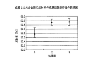
図8参照
図8は、3枚のウェハ上にAl合金を成膜した場合のAl合金膜の反射率の成膜回数依存性の説明図であり、1枚目のウェハの反射率が最も低くなっている。
See FIG.
FIG. 8 is an explanatory diagram of the dependency of the reflectance of the Al alloy film when the Al alloy is formed on three wafers, and the reflectance of the first wafer is the lowest. .
この様な最初のスパッタリングにおける不純物の悪影響を回避するために、ターゲットの表面をArイオンによりクリーニングし、ターゲットの表面を清浄な状態にする必要が生じる。 In order to avoid such an adverse effect of impurities in the initial sputtering, it is necessary to clean the surface of the target with Ar ions to make the surface of the target clean.
そこで、通常は、スパッタリング成膜を行う場合は、ターゲットの表面に付着した水分や酸化膜を除去するため、製品形成用ウェハ上への成膜に先立って、ダミーウェハへの成膜を行い、それにより、ターゲット表面が清浄になった状態で製品形成用ウェハ上への成膜を行っている。 Therefore, normally, when performing sputtering film formation, in order to remove moisture and oxide film adhering to the surface of the target, film formation on a dummy wafer is performed prior to film formation on the product forming wafer. Thus, film formation is performed on the product forming wafer in a state where the target surface is clean.
或いは、シャッター機構を備えたスパッタリング装置の場合には、製品形成用ウェハを搭載したウェハステージをシャッターで覆い、ダミーウェハを使用せずにシャッターにスパッタリングを行っており(例えば、特許文献1参照)、このように、製品形成用ウェハ上への成膜を行う直前に、プレスパッタリングを行うのが一般的な成膜方法である。 Alternatively, in the case of a sputtering apparatus equipped with a shutter mechanism, a wafer stage on which a product forming wafer is mounted is covered with a shutter, and sputtering is performed on the shutter without using a dummy wafer (for example, see Patent Document 1). As described above, it is a common film forming method to perform pre-sputtering immediately before film formation on a product forming wafer.
また、成膜を行わない装置待機時間中に、ダミーウェハ上への成膜を行い、ターゲットの表面を清浄に保つ方法もある。
上述のプレスパッタリングは、スパッタリング成膜においては不可欠な作業であり、いわば常識的なものとして扱われていることもあり、比較的問題視はされていないが、生産性の面から考えて、決して有益な作業とは言えない。 The above-mentioned pre-sputtering is an indispensable work in sputtering film formation, and it may be treated as a common sense, so it is not considered as a problem, but in terms of productivity, it is never It's not a useful task.
即ち、シャッター機構がない場合には、ダミーウェハが必要となり、そのダミーウェハへプレスパッタリングを実行する時間も必要となり、当然ながらその間、成膜装置は非生産時間となり生産性が低下する。 In other words, when there is no shutter mechanism, a dummy wafer is required, and time for performing pre-sputtering on the dummy wafer is also required. Of course, the film forming apparatus is non-production time, and productivity is lowered.
また、シャッター機構がある場合には、ダミーウェハは必要ではないが、シャッター上へプレスパッタリングを実行する時間が必要であることには変わりはなく、当然ながらその間、成膜装置は非生産時間となり生産性が低下する。 In addition, if there is a shutter mechanism, a dummy wafer is not necessary, but there is no change in the time required to perform pre-sputtering on the shutter. Sex is reduced.
また、プレスパッタリングを実行するにあたり、ターゲットが消費されてターゲットの寿命が短くなるとともに、プレスパッタリングによる成膜が加わるため成膜装置内の洗浄周期が短くなり、加えて内部部品の交換周期も短くなる。 In addition, when performing pre-sputtering, the target is consumed and the life of the target is shortened, and since film formation by pre-sputtering is added, the cleaning cycle in the film forming apparatus is shortened, and in addition, the replacement cycle of internal components is also shortened. Become.
今後、生産性向上を鑑みて、ウェハの大口径化が進む中、スパッタリング装置等の成膜装置のランニングコストは、製品処理の増加に伴い大きくなることが予想され、特に、ダミーに用いるウェハの価格は決して無視できるものではない。 In the future, in view of productivity improvement, the running cost of a film forming apparatus such as a sputtering apparatus is expected to increase with an increase in product processing as the diameter of the wafer advances. Price is never negligible.
したがって、本発明は、ダミーウェハを用いることなく且つターゲットを無駄に消費することなく、ターゲットの表面を清浄にすることを目的とする。 Accordingly, an object of the present invention is to clean the surface of a target without using a dummy wafer and without consuming the target wastefully.
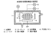
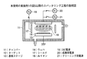
図1は本発明の原理的構成図であり、ここで図1を参照して、本発明における課題を解決するための手段を説明するが、図における符号1及び3は夫々成膜室及び対向電極である。
図1参照
上記課題を解決するために、本発明は、物理的堆積(PVD)装置のターゲット2のクリーニング方法において、成膜を行わない時間に、ターゲット2の表面にターゲット2の構成物質の昇華エネルギーの6倍以下のエネルギーの不活性イオン4を照射してターゲット2の表面をクリーニングすることを特徴とする。
FIG. 1 is a block diagram showing the principle of the present invention. Here, referring to FIG. 1, means for solving the problems in the present invention will be explained. Electrode.
See FIG. 1 In order to solve the above-described problem, the present invention provides a method for cleaning a
このように、成膜を行わない時間に、ターゲット2の表面にターゲット2の構成物質の昇華エネルギーの6倍以下、好適には5倍以下、より好適には4倍以下のエネルギーの不活性イオン4を照射することにより、ターゲット2を無駄に消費することなくターゲット2の表面の清浄化が可能になるとともに、ダミーウェハを必要とすることなく、それによって、製造時間の短縮と低コスト化が可能になる。
In this way, during the time when film formation is not performed, the inert ions having an energy of 6 times or less, preferably 5 times or less, more preferably 4 times or less of the sublimation energy of the constituent material of the
即ち、スパッタ率は、イオンエネルギーと相関関係があり、イオンエネルギーが100eV以下の比較的低い領域では、スパッタ率はイオンエネルギーの2乗に比例し、イオンエネルギーを下げると、スパッタリングが起きなくなるイオンエネルギー値が存在することが知られている。 That is, the sputtering rate has a correlation with the ion energy, and in a relatively low region where the ion energy is 100 eV or less, the sputtering rate is proportional to the square of the ion energy, and when the ion energy is lowered, the ion energy at which sputtering does not occur. It is known that a value exists.
このスパッタリングが起きなくなるイオンエネルギー値をしきい値エネルギーと言い、このイオンエネルギー以下では、スパッタ率は0となる。
このしきい値エネルギーは、スパッタリングの条件や、ターゲット2の材質により異なるが、一般的には、ターゲット2の材質の昇華エネルギーの4倍とされている。
The ion energy value at which this sputtering does not occur is called threshold energy, and below this ion energy, the sputtering rate becomes zero.
This threshold energy varies depending on the sputtering conditions and the material of the
したがって、このしきい値エネルギー以下のイオンパワーで不活性イオン4をターゲット2の表面に照射することで、ターゲット母材のスパッタリングを起こすことなく、不純物の除去、あるいは不純分子の付着を防止することが可能となる。
Therefore, by irradiating the surface of the
即ち、ターゲット母材はスパッタリングされないので、ターゲット2および内部治具の使用可能時間に影響せず、かつパーティクルが発生する問題も生じないので、パーティクルがスパッタリング工程における成膜に影響を与えることはなく、常に安定した特性の膜を成膜することができる。
That is, since the target base material is not sputtered, the usable time of the
但し、照射するイオンエネルギーは厳密にしきい値エネルギー以下である必要はなく、しきい値エネルギーの1.5倍以下、即ち、昇華エネルギーとしては6倍以下であれば、スパッタリングは殆ど起こらないため、ターゲット2の消耗を従来に比べて大幅に低減することができる。
However, the ion energy to be irradiated does not need to be strictly lower than the threshold energy, and sputtering is hardly caused if the threshold energy is 1.5 times or less, that is, if the sublimation energy is 6 times or less, The consumption of the
また、物理的堆積装置にはターゲット2から飛び出す物質を被成膜基板以外の箇所へ飛散することを防ぐシールド5を備えることが望ましく、クリーニング工程中にシールド5に不活性イオン4を排斥する極性の直流電圧を印加することが望ましい。
In addition, the physical deposition apparatus preferably includes a shield 5 that prevents the material that jumps out of the
このように、シールド5を設け、このシールド5に直流電圧を印加することによって、低電圧下において安定な放電を維持しやすくなるとともに、放電を発生させるトリガーの作用も期待できる。 Thus, by providing the shield 5 and applying a DC voltage to the shield 5, it becomes easy to maintain a stable discharge under a low voltage, and a trigger action for generating a discharge can be expected.
また、クリーニング工程は、物理的堆積装置の待機時間中に常時行うことが望ましく、その場合には、ターゲット2の消費が極力起こらないように、昇華エネルギーの4倍以下のイオンエネルギーで行うことが望ましい。
Further, it is desirable that the cleaning process is always performed during the standby time of the physical deposition apparatus, and in that case, the cleaning process is performed with ion energy that is four times or less the sublimation energy so that the
或いは、クリーニング工程は、必要な時のみ行うようにしても良く、この場合にはクリーニング時間が短くなるのでクリーニング効率を高めるために、昇華エネルギーの6倍以下のイオンエネルギーで行うことが望ましい。 Alternatively, the cleaning process may be performed only when necessary. In this case, since the cleaning time is shortened, it is desirable to perform the ion energy with 6 times or less of the sublimation energy in order to increase the cleaning efficiency.
また、物理的堆積装置としては、ターゲット2に電力を供給する電源系を、成膜のためのスパッタリングを行う第1の電源6と、クリーニングを行うための第2の電源7とで構成するこが望ましく、それによって、スパッタリング工程とクリーニング工程の切替えをスムーズに行うことができる。
As a physical deposition apparatus, a power supply system that supplies power to the
なお、本発明における物理的堆積装置としては、スパッタリング装置が最も典型的なものであるが、レーザアブレーション装置等にも適用されるものであり、その場合には、クリーニング用の放電電極を設ければ良い。 As a physical deposition apparatus in the present invention, a sputtering apparatus is the most typical one, but it can also be applied to a laser ablation apparatus or the like. In that case, a cleaning discharge electrode is provided. It ’s fine.
また、照射する不活性ガスとしてはArガスが典型的なものであるが、Kr或いはXe等の他の希ガスを用いても良いものである。
また、ターゲット母材としては、金属が典型的なものであるが、酸化物等の非金属ダーゲットにも適用されるものである。
The inert gas to be irradiated is typically Ar gas, but other rare gases such as Kr or Xe may be used.
The target base material is typically a metal, but is also applicable to non-metal target such as oxide.
本発明においては、ダミーウェハを使用することなく、ターゲットを消費することなく、且つ、生産時間を低減することなく、ターゲット表面を常時清浄な状態に保つことができ、それによって、成膜した膜の性質を再現性良く良好に保つことができ、ひいては、製品の低コスト化・高品質化に寄与するところが大きい。 In the present invention, the target surface can be kept clean at all times without using a dummy wafer, without consuming the target, and without reducing the production time. The properties can be kept well with good reproducibility, and this contributes greatly to cost reduction and high quality of the product.
本発明は、成膜していない待機時間中に、ターゲットの表面をスパッタリングが起きないイオンパワーでArイオンを照射して、不純物の除去、あるいは不純分子の付着を防止するものである。 In the present invention, Ar ions are irradiated on the surface of a target with ion power that does not cause sputtering during a standby time during which no film is formed, thereby preventing impurities from being removed or impure molecules from being attached.
この場合、ターゲットから飛び出す物質を基板以外の箇所へ飛散することを防ぐためのシールドを設け、このシールドに直流電圧を印加することによって、低電圧においても安定な放電状態を実現するものである。 In this case, by providing a shield for preventing the substance jumping out from the target from being scattered to a place other than the substrate, and applying a DC voltage to the shield, a stable discharge state is realized even at a low voltage.
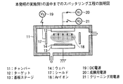
ここで、図2乃至図6を参照して、本発明の実施例1のターゲットのクリーニング方法を説明するが、まず、図2を参照して本発明の実施例1に用いるスパッタリング装置を説明する。
図2参照
図2は、本発明の実施例1のスパッタリング装置の概略的構成図であり、例えば、Al合金製のチャンバー11、一方の放電電極を兼ねるターゲット12、ターゲット12に対向する他方の放電電極を兼ねるとともに被処理基板となるウェハ14を載置するための基板ステージ13、チャンバー11内を高真空に排気するクライオポンプ15、チャンバー11内のArガスを供給するMFC(マスフローコントローラ)16、スパッタリングされたターゲット母材が、ウェハ14以外の個所に飛散することを防ぐシールド17、シールド17にArイオン18の衝突を防ぐ電圧を印加するためのDC電源19、成膜用電源20、及び、クリーニング用電源21から構成される。
Here, the target cleaning method according to the first embodiment of the present invention will be described with reference to FIGS. 2 to 6. First, the sputtering apparatus used in the first embodiment of the present invention will be described with reference to FIG. .
See Figure 2
FIG. 2 is a schematic configuration diagram of the sputtering apparatus according to the first embodiment of the present invention. For example, the
この場合、成膜用電源20は、10kW以上の条件で使用できるものであり、クリーニング用電源21は、100W以下の条件で使用できるものである。
また、基板ステージ13は接地して使用する。
In this case, the film-forming
The
次に、図3乃至図6を参照して、本発明の実施例1のターゲットのクリーニング工程を含むスパッタリング工程を説明するが、ここでは、Al合金製のターゲットを用いたAl合金膜の成膜工程として説明する。
図3参照
まず、ウェハ14を基板ステージ13に載置した状態で、MFC16からチャンバー11内へArガスを例えば、50sccm流し、チャンバー11内の圧力を例えば2mTorrに安定させてから、成膜用電源20を用いてAl合金製のターゲット12に500Vで15kWのDCパワーを印加して、ウェハ14上にスパッタリング成膜を行う。
なお、この時、シールド17に対しては無バイアスである。
Next, a sputtering process including a target cleaning process according to the first embodiment of the present invention will be described with reference to FIGS. 3 to 6. Here, an Al alloy film is formed using an Al alloy target. This will be described as a process.
See Figure 3
First, with the
At this time, no bias is applied to the
図4参照
次いで、成膜終了したウェハ14をチャンバー11の外に取り出したのち、チャンバー11内をクライオポンプ15を用いて1×10⁻⁸Torr以下のベース圧力に排気する。 この場合、高真空であるほど、不純分子のターゲット表面への付着は促進するため、ウェハ14からの脱ガスを含めて、成膜時の残留ガスを極力排気する。
See Figure 4
Next, after the film-formed
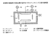
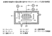
図5参照
次いで、MFC16からチャンバー11内へArガスを例えば、500sccm流し、チャンバー11内の圧力を例えば、10mTorrに安定させてから、クリーニング用電源21を用いてターゲット12に−100Vで50WのDCパワーを印加するとともに、シールド17に+30Vの電圧を印加してターゲット12の表面にArイオン18を照射してクリーニングを行う。
See Figure 5
Next, Ar gas is flowed from the
この場合、Arイオン18のイオンエネルギーはしきい値エネルギー以下となるので、スパッタ率が0の状態でイオンクリーニングが開始され、次の成膜工程までの待機時間の間、常に放電を維持してクリーニングを継続して行う。
なお、しきい値エネルギーはターゲット11の材質等により異なるが、ターゲット母材の昇華エネルギーの4倍であり、通常は20〜100eVの範囲内である。
In this case, since the ion energy of the
The threshold energy varies depending on the material of the
また、クリーニングに際して、シールド17には正の電荷を有するArイオン18を排斥する極性の正の直流電圧を印加しているので、低電圧においても放電を安定に維持することができるとともに、クリーニング用の放電を発生させる場合のトリガー作用も期待できる。
Further, during cleaning, a positive DC voltage having a polarity that eliminates
図6参照
次いで、クリーニング用電源21をオフにしたのち、次のウェハ14を基板ステージ13に載置した状態で、再び、MFC16からチャンバー11内へArガスを例えば、50sccm流し、チャンバー11内の圧力を例えば2mTorrに安定させてから、成膜用電源20を用いてターゲット12に500Vで15kWのDCパワーを印加して、ウェハ14上にスパッタリング成膜を行う。
See FIG.
Next, after the
以上、説明したように、本発明においては、「成膜→イオンクリーニング→成膜」のように、成膜終了後に直ちにイオンクリーニングを開始して、次の成膜を行うまでの待機時間の間、継続しているので、不純物、特に水分子が付着して、ターゲット11の表面にアルミナ系の酸化物が形成されるのを防止することができる。
因に、アルミナ系の酸化物が形成されてしまうと、スパッタ率0のイオンクリーニングで除去することは困難となる。
As described above, in the present invention, during the waiting time from the start of ion cleaning immediately after the completion of film formation until the next film formation, such as “film formation → ion cleaning → film formation”. Therefore, it is possible to prevent impurities, particularly water molecules, from adhering to the surface of the
If alumina-based oxides are formed, it becomes difficult to remove them by ion cleaning with a sputtering rate of zero.
また、このイオンクリーニングはスパッタ率0の条件で行っているので、イオンクリーニング中にターゲット12が消費されることがなく、したがって、イオンクリーニング中にターゲット母材がスパッタリングされることがないので成膜装置の内部部品の交換周期を長くすることができる。
Further, since this ion cleaning is performed under the condition of a sputtering rate of 0, the
さらに、待機時間を利用して常にクリーニングを行っているので、成膜工程をウェハ挿入後直ちに開始することができ、従来のように成膜工程に先立ってプレスパッタリングを行う必要がないので生産性を向上することができる。 Furthermore, since the cleaning is always performed using the waiting time, the film forming process can be started immediately after the wafer is inserted, and it is not necessary to perform the pre-sputtering prior to the film forming process as in the prior art. Can be improved.
以上、本発明の実施例を説明してきたが、本発明は実施例に記載した条件・構成に限られるものではなく、各種の変更が可能であり、例えば、実施例に記載した印加電圧、圧力等の数値は記載した数値に限られるものではない。 The embodiments of the present invention have been described above, but the present invention is not limited to the conditions and configurations described in the embodiments, and various modifications are possible. For example, the applied voltage and pressure described in the embodiments The numerical values such as are not limited to the numerical values described.
また、上記の実施例の説明においては、Al合金の成膜工程として説明しているが、Al合金の成膜工程に限られるものではなく、TiN,Ti等の他の金属の成膜工程、NiFeやPdPtMn等の磁性膜の成膜工程にも適用されるものであり、さらには、酸化物超伝導体等の酸化物或いは他の絶縁体等の成膜工程にも適用されるものである。 In the description of the above embodiment, the Al alloy film forming process is described. However, the present invention is not limited to the Al alloy film forming process, and other metal film forming processes such as TiN and Ti, It is also applied to a film forming process of a magnetic film such as NiFe or PdPtMn, and further applied to a film forming process of an oxide such as an oxide superconductor or another insulator. .
また、上記の実施例の説明においてはイオンクリーニングを待機時間中常に行っているが、スパッタリング装置の運用に応じては、ある一定周期でイオンクリーニングを実行するように、即ち、「成膜→待機→イオンクリーニング→待機→成膜」というサイクルで行っても良いものである。 In the description of the above embodiment, the ion cleaning is always performed during the standby time. However, depending on the operation of the sputtering apparatus, the ion cleaning is performed at a certain period, that is, “film formation → standby”. It may be performed in a cycle of “→ ion cleaning → standby → film formation”.
また、上記の実施例の説明においては、イオンクリーニングをスパッタ率0の条件で行っているが、必ずしもスパッタ率0である必要はなく、例えば、しきい値エネルギーの1.5倍以下であればターゲットの消費が少ないので問題はなく、特に、上述の「成膜→待機→イオンクリーニング→待機→成膜」というサイクルの場合には、クリーニング時間が短いのでしきい値エネルギーの1.5倍以下の範囲内でより高いイオンエネルギーで行った方がクリニーング効果が高まる。 In the description of the above embodiment, ion cleaning is performed under the condition of a sputtering rate of 0. However, the sputtering rate does not necessarily have to be 0. There is no problem because the consumption of the target is small. Especially, in the case of the above-described cycle of “film formation → standby → ion cleaning → standby → film formation”, the cleaning time is short, so the threshold energy is 1.5 times or less. When the ion energy is higher than the above range, the cleaning effect is enhanced.
また、上記の実施例の説明においては、Arガスを用いているが、Arガスに限られるものではなく、XeガスやKrガス等の希ガスを用いても良いものである。 In the description of the above embodiment, Ar gas is used. However, it is not limited to Ar gas, and rare gas such as Xe gas or Kr gas may be used.
また、上記の実施例の説明においては、成膜用のガスとイオンクリニーング用のガスを同じガス種としているが、互いに異なったガス種を用いても良いものである。 Further, in the description of the above embodiment, the film forming gas and the ion cleaning gas are the same gas type, but different gas types may be used.
また、上記の実施例の説明においては、成膜用電源とクリニーング用電源を別電源としているが、単一の可変電圧電源を用いても良いものである。 In the above description of the embodiment, the film forming power source and the cleaning power source are separate power sources, but a single variable voltage power source may be used.
また、上記の実施例の説明においては、イオンクリーニング工程においてシールドに直流電圧を印加しているが、必ずしもシールドに電圧を印加する必要はないものであり、さらには、シールドを具備しないタイプのスパッタリング装置にも適用されるものである。 In the description of the above embodiment, a DC voltage is applied to the shield in the ion cleaning process, but it is not always necessary to apply a voltage to the shield. This also applies to the device.
また、上記の実施例の説明においては、直流電力を用いてスパッタリングを行っているが、交流電力を用いてスパッタリングを行っても良いことが言うまでもない。 Moreover, in the description of the above embodiment, sputtering is performed using DC power, but it goes without saying that sputtering may be performed using AC power.
また、上記の実施例の説明においては、成膜装置をスパッタリング装置として説明しているが、スパッタリング装置に限られるものではなく、レーザアブレーション装置等のターゲットを用いて成膜を行う他の物理的堆積装置にも適用されるものであり、当該装置が放電用電極を具備していない場合には、ターゲットが一方の電極となるようにクリーニング用の放電電極構造を設ければ良い。 In the description of the above embodiment, the film forming apparatus is described as a sputtering apparatus. However, the present invention is not limited to the sputtering apparatus, and other physical processes for forming a film using a target such as a laser ablation apparatus. The present invention is also applicable to a deposition apparatus. When the apparatus does not include a discharge electrode, a cleaning discharge electrode structure may be provided so that the target is one electrode.
また、上記の実施例の説明においては、シングルターゲットの成膜装置として説明しているが、マルチターゲットを用いる成膜装置にも適用されることはいうまでもない。 In the description of the above embodiments, the film is described as a single target film forming apparatus, but it goes without saying that the present invention is also applicable to a film forming apparatus using a multi target.
本発明の活用例としては、スパッタリング装置のターゲットのイオンクリーニング工程が典型的なものであるが、ターゲットを用いて成膜を行う他の物理的堆積装置にも適用されるものである。 As an application example of the present invention, a target ion cleaning process of a sputtering apparatus is typical, but the present invention is also applicable to other physical deposition apparatuses that perform film formation using a target.
1 成膜室
2 ターゲット
3 対向電極
4 不活性イオン
5 シールド
6 第1の電源
7 第2の電源
11 チャンバー
12 ターゲット
13 基板ステージ
14 ウェハ
15 クライオポンプ
16 MFC
17 シールド
18 Arイオン
19 DC電源
20 成膜用電源
21 クリーニング用電源
DESCRIPTION OF
17
Claims (5)
Priority Applications (1)
| Application Number | Priority Date | Filing Date | Title |
|---|---|---|---|
| JP2004116373A JP2005298894A (en) | 2004-04-12 | 2004-04-12 | Target cleaning method and physical deposition apparatus |
Applications Claiming Priority (1)
| Application Number | Priority Date | Filing Date | Title |
|---|---|---|---|
| JP2004116373A JP2005298894A (en) | 2004-04-12 | 2004-04-12 | Target cleaning method and physical deposition apparatus |
Publications (1)
| Publication Number | Publication Date |
|---|---|
| JP2005298894A true JP2005298894A (en) | 2005-10-27 |
Family
ID=35330806
Family Applications (1)
| Application Number | Title | Priority Date | Filing Date |
|---|---|---|---|
| JP2004116373A Pending JP2005298894A (en) | 2004-04-12 | 2004-04-12 | Target cleaning method and physical deposition apparatus |
Country Status (1)
| Country | Link |
|---|---|
| JP (1) | JP2005298894A (en) |
Cited By (6)
| Publication number | Priority date | Publication date | Assignee | Title |
|---|---|---|---|---|
| WO2008032461A1 (en) * | 2006-09-14 | 2008-03-20 | Shimadzu Corporation | Method for fabricating light or radiation detector, and light or radiation detector |
| JP2009010240A (en) * | 2007-06-29 | 2009-01-15 | Ulvac Japan Ltd | Plasma processing method |
| JP2009065181A (en) * | 2006-03-03 | 2009-03-26 | Canon Anelva Corp | Method for manufacturing magnetoresistive element |
| JP2010212234A (en) * | 2009-02-13 | 2010-09-24 | Y S Denshi Kogyo Kk | Plasma generator |
| WO2011007580A1 (en) * | 2009-07-17 | 2011-01-20 | 株式会社アルバック | Substrate processing method |
| US8367156B2 (en) | 2006-03-03 | 2013-02-05 | Canon Anelva Corporation | Method of manufacturing magnetoresistive device and apparatus for manufacturing the same |
-
2004
- 2004-04-12 JP JP2004116373A patent/JP2005298894A/en active Pending
Cited By (14)
| Publication number | Priority date | Publication date | Assignee | Title |
|---|---|---|---|---|
| US8367156B2 (en) | 2006-03-03 | 2013-02-05 | Canon Anelva Corporation | Method of manufacturing magnetoresistive device and apparatus for manufacturing the same |
| JP2009065181A (en) * | 2006-03-03 | 2009-03-26 | Canon Anelva Corp | Method for manufacturing magnetoresistive element |
| US10629804B2 (en) | 2006-03-03 | 2020-04-21 | Canon Anelva Corporation | Method of manufacturing magnetoresistive device |
| US7736941B2 (en) | 2006-09-14 | 2010-06-15 | Shimadzu Corporation | Light or radiation detector manufacturing method |
| WO2008032461A1 (en) * | 2006-09-14 | 2008-03-20 | Shimadzu Corporation | Method for fabricating light or radiation detector, and light or radiation detector |
| JP2009010240A (en) * | 2007-06-29 | 2009-01-15 | Ulvac Japan Ltd | Plasma processing method |
| JP2010212234A (en) * | 2009-02-13 | 2010-09-24 | Y S Denshi Kogyo Kk | Plasma generator |
| KR20120046223A (en) * | 2009-07-17 | 2012-05-09 | 가부시키가이샤 알박 | Substrate processing method |
| CN102482758A (en) * | 2009-07-17 | 2012-05-30 | 爱发科股份有限公司 | Substrate processing method |
| CN102482758B (en) * | 2009-07-17 | 2014-04-30 | 爱发科股份有限公司 | Substrate processing method |
| US8956513B2 (en) | 2009-07-17 | 2015-02-17 | Ulvac, Inc. | Substrate processing method |
| JP5731383B2 (en) * | 2009-07-17 | 2015-06-10 | 株式会社アルバック | Substrate processing method |
| KR101685061B1 (en) | 2009-07-17 | 2016-12-09 | 가부시키가이샤 알박 | Substrate processing method |
| WO2011007580A1 (en) * | 2009-07-17 | 2011-01-20 | 株式会社アルバック | Substrate processing method |
Similar Documents
| Publication | Publication Date | Title |
|---|---|---|
| US10002745B2 (en) | Plasma treatment process for in-situ chamber cleaning efficiency enhancement in plasma processing chamber | |
| US8206829B2 (en) | Plasma resistant coatings for plasma chamber components | |
| KR101083148B1 (en) | Plasma etching method, plasma etching apparatus, and storage medium | |
| TWI525694B (en) | Chamber cleaning method | |
| JP5442403B2 (en) | Substrate processing apparatus, cleaning method therefor, and recording medium recording program | |
| US11127568B2 (en) | Plasma etching apparatus | |
| US9653317B2 (en) | Plasma processing method and plasma processing apparatus | |
| KR20100009625A (en) | Silicide forming method and system thereof | |
| KR20190008227A (en) | Etching method | |
| JP4716566B2 (en) | Plasma processing chamber for reducing copper oxide on a substrate and method thereof | |
| US20100218786A1 (en) | Cleaning method of plasma processing apparatus and storage medium | |
| JP2016086046A (en) | Plasma processing method | |
| JP2017212357A (en) | Plasma processing method | |
| JP2005298894A (en) | Target cleaning method and physical deposition apparatus | |
| JP2007042818A (en) | Film forming apparatus and film forming method | |
| JP5704192B2 (en) | Plasma etching method, plasma etching apparatus, and storage medium | |
| JP6005288B2 (en) | Method for forming oxide thin film | |
| KR101190804B1 (en) | Plasma processing method | |
| US20040007248A1 (en) | Method for improving reliability of reaction apparatus | |
| JP5312138B2 (en) | Sputtering method | |
| US20250308881A1 (en) | Silicon etch byproduct removal | |
| JP2008171874A (en) | Method and apparatus for manufacturing dielectric thin film | |
| JP2004107774A (en) | Sputter film forming method, sputter film forming apparatus, and method of manufacturing electro-optical device | |
| JP2006032602A (en) | Sputtering apparatus and method | |
| JP2002313736A (en) | Plasma treating equipment |
Legal Events
| Date | Code | Title | Description |
|---|---|---|---|
| A621 | Written request for application examination |
Free format text: JAPANESE INTERMEDIATE CODE: A621 Effective date: 20070223 |
|
| A711 | Notification of change in applicant |
Free format text: JAPANESE INTERMEDIATE CODE: A712 Effective date: 20080730 |
|
| A977 | Report on retrieval |
Free format text: JAPANESE INTERMEDIATE CODE: A971007 Effective date: 20090831 |
|
| A131 | Notification of reasons for refusal |
Free format text: JAPANESE INTERMEDIATE CODE: A131 Effective date: 20090908 |
|
| A02 | Decision of refusal |
Free format text: JAPANESE INTERMEDIATE CODE: A02 Effective date: 20100112 |