WO2011105056A1 - 電子デバイスおよび電子デバイスの製造方法 - Google Patents
電子デバイスおよび電子デバイスの製造方法 Download PDFInfo
- Publication number
- WO2011105056A1 WO2011105056A1 PCT/JP2011/000991 JP2011000991W WO2011105056A1 WO 2011105056 A1 WO2011105056 A1 WO 2011105056A1 JP 2011000991 W JP2011000991 W JP 2011000991W WO 2011105056 A1 WO2011105056 A1 WO 2011105056A1
- Authority
- WO
- WIPO (PCT)
- Prior art keywords
- insulating film
- compound semiconductor
- group
- electronic device
- crystal
- Prior art date
- Legal status (The legal status is an assumption and is not a legal conclusion. Google has not performed a legal analysis and makes no representation as to the accuracy of the status listed.)
- Ceased
Links
Images



Classifications
-
- H—ELECTRICITY
- H10—SEMICONDUCTOR DEVICES; ELECTRIC SOLID-STATE DEVICES NOT OTHERWISE PROVIDED FOR
- H10D—INORGANIC ELECTRIC SEMICONDUCTOR DEVICES
- H10D84/00—Integrated devices formed in or on semiconductor substrates that comprise only semiconducting layers, e.g. on Si wafers or on GaAs-on-Si wafers
- H10D84/01—Manufacture or treatment
-
- H—ELECTRICITY
- H10—SEMICONDUCTOR DEVICES; ELECTRIC SOLID-STATE DEVICES NOT OTHERWISE PROVIDED FOR
- H10D—INORGANIC ELECTRIC SEMICONDUCTOR DEVICES
- H10D84/00—Integrated devices formed in or on semiconductor substrates that comprise only semiconducting layers, e.g. on Si wafers or on GaAs-on-Si wafers
-
- H—ELECTRICITY
- H10—SEMICONDUCTOR DEVICES; ELECTRIC SOLID-STATE DEVICES NOT OTHERWISE PROVIDED FOR
- H10D—INORGANIC ELECTRIC SEMICONDUCTOR DEVICES
- H10D84/00—Integrated devices formed in or on semiconductor substrates that comprise only semiconducting layers, e.g. on Si wafers or on GaAs-on-Si wafers
- H10D84/01—Manufacture or treatment
- H10D84/0123—Integrating together multiple components covered by H10D12/00 or H10D30/00, e.g. integrating multiple IGBTs
- H10D84/0126—Integrating together multiple components covered by H10D12/00 or H10D30/00, e.g. integrating multiple IGBTs the components including insulated gates, e.g. IGFETs
-
- H—ELECTRICITY
- H10—SEMICONDUCTOR DEVICES; ELECTRIC SOLID-STATE DEVICES NOT OTHERWISE PROVIDED FOR
- H10D—INORGANIC ELECTRIC SEMICONDUCTOR DEVICES
- H10D84/00—Integrated devices formed in or on semiconductor substrates that comprise only semiconducting layers, e.g. on Si wafers or on GaAs-on-Si wafers
- H10D84/01—Manufacture or treatment
- H10D84/02—Manufacture or treatment characterised by using material-based technologies
- H10D84/03—Manufacture or treatment characterised by using material-based technologies using Group IV technology, e.g. silicon technology or silicon-carbide [SiC] technology
- H10D84/038—Manufacture or treatment characterised by using material-based technologies using Group IV technology, e.g. silicon technology or silicon-carbide [SiC] technology using silicon technology, e.g. SiGe
-
- H—ELECTRICITY
- H10—SEMICONDUCTOR DEVICES; ELECTRIC SOLID-STATE DEVICES NOT OTHERWISE PROVIDED FOR
- H10D—INORGANIC ELECTRIC SEMICONDUCTOR DEVICES
- H10D84/00—Integrated devices formed in or on semiconductor substrates that comprise only semiconducting layers, e.g. on Si wafers or on GaAs-on-Si wafers
- H10D84/80—Integrated devices formed in or on semiconductor substrates that comprise only semiconducting layers, e.g. on Si wafers or on GaAs-on-Si wafers characterised by the integration of at least one component covered by groups H10D12/00 or H10D30/00, e.g. integration of IGFETs
- H10D84/82—Integrated devices formed in or on semiconductor substrates that comprise only semiconducting layers, e.g. on Si wafers or on GaAs-on-Si wafers characterised by the integration of at least one component covered by groups H10D12/00 or H10D30/00, e.g. integration of IGFETs of only field-effect components
- H10D84/83—Integrated devices formed in or on semiconductor substrates that comprise only semiconducting layers, e.g. on Si wafers or on GaAs-on-Si wafers characterised by the integration of at least one component covered by groups H10D12/00 or H10D30/00, e.g. integration of IGFETs of only field-effect components of only insulated-gate FETs [IGFET]
-
- H—ELECTRICITY
- H10—SEMICONDUCTOR DEVICES; ELECTRIC SOLID-STATE DEVICES NOT OTHERWISE PROVIDED FOR
- H10W—GENERIC PACKAGES, INTERCONNECTIONS, CONNECTORS OR OTHER CONSTRUCTIONAL DETAILS OF DEVICES COVERED BY CLASS H10
- H10W72/00—Interconnections or connectors in packages
- H10W72/01—Manufacture or treatment
- H10W72/019—Manufacture or treatment of bond pads
-
- H—ELECTRICITY
- H10—SEMICONDUCTOR DEVICES; ELECTRIC SOLID-STATE DEVICES NOT OTHERWISE PROVIDED FOR
- H10W—GENERIC PACKAGES, INTERCONNECTIONS, CONNECTORS OR OTHER CONSTRUCTIONAL DETAILS OF DEVICES COVERED BY CLASS H10
- H10W74/00—Encapsulations, e.g. protective coatings
- H10W74/10—Encapsulations, e.g. protective coatings characterised by their shape or disposition
- H10W74/111—Encapsulations, e.g. protective coatings characterised by their shape or disposition the semiconductor body being completely enclosed
- H10W74/114—Encapsulations, e.g. protective coatings characterised by their shape or disposition the semiconductor body being completely enclosed by a substrate and the encapsulations
-
- H—ELECTRICITY
- H10—SEMICONDUCTOR DEVICES; ELECTRIC SOLID-STATE DEVICES NOT OTHERWISE PROVIDED FOR
- H10W—GENERIC PACKAGES, INTERCONNECTIONS, CONNECTORS OR OTHER CONSTRUCTIONAL DETAILS OF DEVICES COVERED BY CLASS H10
- H10W74/00—Encapsulations, e.g. protective coatings
- H10W74/10—Encapsulations, e.g. protective coatings characterised by their shape or disposition
- H10W74/131—Encapsulations, e.g. protective coatings characterised by their shape or disposition the semiconductor body being only partially enclosed
- H10W74/137—Encapsulations, e.g. protective coatings characterised by their shape or disposition the semiconductor body being only partially enclosed the encapsulations being directly on the semiconductor body
-
- H—ELECTRICITY
- H10—SEMICONDUCTOR DEVICES; ELECTRIC SOLID-STATE DEVICES NOT OTHERWISE PROVIDED FOR
- H10W—GENERIC PACKAGES, INTERCONNECTIONS, CONNECTORS OR OTHER CONSTRUCTIONAL DETAILS OF DEVICES COVERED BY CLASS H10
- H10W74/00—Encapsulations, e.g. protective coatings
- H10W74/10—Encapsulations, e.g. protective coatings characterised by their shape or disposition
- H10W74/131—Encapsulations, e.g. protective coatings characterised by their shape or disposition the semiconductor body being only partially enclosed
- H10W74/147—Encapsulations, e.g. protective coatings characterised by their shape or disposition the semiconductor body being only partially enclosed the encapsulations being multilayered
-
- H—ELECTRICITY
- H10—SEMICONDUCTOR DEVICES; ELECTRIC SOLID-STATE DEVICES NOT OTHERWISE PROVIDED FOR
- H10W—GENERIC PACKAGES, INTERCONNECTIONS, CONNECTORS OR OTHER CONSTRUCTIONAL DETAILS OF DEVICES COVERED BY CLASS H10
- H10W72/00—Interconnections or connectors in packages
- H10W72/01—Manufacture or treatment
- H10W72/0198—Manufacture or treatment batch processes
-
- H—ELECTRICITY
- H10—SEMICONDUCTOR DEVICES; ELECTRIC SOLID-STATE DEVICES NOT OTHERWISE PROVIDED FOR
- H10W—GENERIC PACKAGES, INTERCONNECTIONS, CONNECTORS OR OTHER CONSTRUCTIONAL DETAILS OF DEVICES COVERED BY CLASS H10
- H10W72/00—Interconnections or connectors in packages
- H10W72/20—Bump connectors, e.g. solder bumps or copper pillars; Dummy bumps; Thermal bumps
- H10W72/241—Dispositions, e.g. layouts
- H10W72/242—Dispositions, e.g. layouts relative to the surface, e.g. recessed, protruding
-
- H—ELECTRICITY
- H10—SEMICONDUCTOR DEVICES; ELECTRIC SOLID-STATE DEVICES NOT OTHERWISE PROVIDED FOR
- H10W—GENERIC PACKAGES, INTERCONNECTIONS, CONNECTORS OR OTHER CONSTRUCTIONAL DETAILS OF DEVICES COVERED BY CLASS H10
- H10W72/00—Interconnections or connectors in packages
- H10W72/20—Bump connectors, e.g. solder bumps or copper pillars; Dummy bumps; Thermal bumps
- H10W72/29—Bond pads specially adapted therefor
-
- H—ELECTRICITY
- H10—SEMICONDUCTOR DEVICES; ELECTRIC SOLID-STATE DEVICES NOT OTHERWISE PROVIDED FOR
- H10W—GENERIC PACKAGES, INTERCONNECTIONS, CONNECTORS OR OTHER CONSTRUCTIONAL DETAILS OF DEVICES COVERED BY CLASS H10
- H10W72/00—Interconnections or connectors in packages
- H10W72/90—Bond pads, in general
- H10W72/941—Dispositions of bond pads
- H10W72/9415—Dispositions of bond pads relative to the surface, e.g. recessed, protruding
-
- H—ELECTRICITY
- H10—SEMICONDUCTOR DEVICES; ELECTRIC SOLID-STATE DEVICES NOT OTHERWISE PROVIDED FOR
- H10W—GENERIC PACKAGES, INTERCONNECTIONS, CONNECTORS OR OTHER CONSTRUCTIONAL DETAILS OF DEVICES COVERED BY CLASS H10
- H10W72/00—Interconnections or connectors in packages
- H10W72/90—Bond pads, in general
- H10W72/941—Dispositions of bond pads
- H10W72/942—Dispositions of bond pads relative to underlying supporting features, e.g. bond pads, RDLs or vias
Definitions
- the present invention relates to an electronic device and a method for manufacturing the electronic device.
- Patent Document 1 discloses a technique of a wafer level package using a silicon substrate and having high airtightness. Wafer level package technology makes it possible to encapsulate semiconductor elements in a thin and chip size.
- Patent Document 1 Japanese Patent Application Laid-Open No. 2001-68580
- the silicon substrate is not an insulator, if a compound semiconductor crystal, an electrode and a wiring are provided above the silicon substrate, a leakage current from the compound semiconductor crystal to the silicon substrate may occur. Furthermore, the high frequency characteristics of signals input to and output from the compound semiconductor crystal may deteriorate due to the effect of stray capacitance in the high frequency band between the compound semiconductor crystal and the silicon substrate.
- a compound semiconductor crystal when a compound semiconductor crystal is epitaxially grown on a silicon substrate, an inhibitor that inhibits the growth of the compound semiconductor crystal is formed on the silicon substrate, a small opening is formed in the inhibitor, and a seed such as germanium is formed in the opening.
- a method is conceivable in which a compound semiconductor crystal is selectively epitaxially grown on a seed body after the body is selectively grown.
- a step is formed between the epitaxially grown compound semiconductor crystal and the inhibitor.
- the formed wiring may be disconnected due to a step.
- a base substrate whose surface is a silicon crystal, a group 3-5 compound semiconductor crystal formed in a partial region on the silicon crystal,
- An electronic element including a part of a group -5 compound semiconductor crystal as an active layer, an insulating film formed on the base substrate, covering the electronic element, an electrode formed on the insulating film, and penetrating the insulating film; At least a portion is formed on the insulating film, the first coupling wiring for electrically coupling the electronic element and the electrode, the passive element formed on the insulating film, and the insulating film are penetrated.
- An electronic device is provided that includes a second coupling wiring that is formed on an insulating film and electrically couples an electronic element and a passive element.
- the electronic device further includes a sealing material that is formed on the insulating film and seals the electrode and the first coupling wiring, and the electrode penetrates the sealing material and is exposed on the surface of the sealing material.
- the group 3-5 compound semiconductor crystal may be formed via a seed body that relaxes the lattice mismatch between the silicon crystal and the group 3-5 compound semiconductor crystal.
- the seed body has a composition of C x Si y Ge z Sn 1-xyz (0 ⁇ x ⁇ 1, 0 ⁇ y ⁇ 1, 0 ⁇ z ⁇ 1, 0 ⁇ x + y + z ⁇ 1). is there.
- the Group 3-5 compound semiconductor crystal is, for example, a GaAs crystal and Al a Ga b In 1-ab N c P d As 1-cd (0 ⁇ 1) lattice-matched or pseudo-lattice-matched to the GaAs crystal. a ⁇ 1, 0 ⁇ b ⁇ 1, 0 ⁇ c ⁇ 1, 0 ⁇ d ⁇ 1, 0 ⁇ a + b ⁇ 1, 0 ⁇ c + d ⁇ 1).
- the electronic device may further include an inhibitor that inhibits the growth of the compound semiconductor crystal on the base substrate, and the seed body may be formed in an opening that is formed in the inhibitor and reaches the base substrate.
- the first coupling wiring and the second coupling wiring extend from the electronic element in a direction perpendicular to the surface where the seed body and the electronic element are in contact.
- the electronic element in the above electronic device is, for example, a transistor, and the transistor and the passive element form a microwave circuit.
- the transistor is, for example, an FET.
- the transistor may be a heterobipolar transistor, and the passive element may include a resistor that prevents thermal runaway of the heterobipolar transistor.
- a base substrate whose surface is a silicon crystal, a plurality of Group 3-5 compound semiconductor crystals formed in a partial region on the silicon crystal, and a plurality of Group 3-5 compounds
- An electronic element including a part of each of the group 3-5 compound semiconductor crystals of the semiconductor crystal as a part of the plurality of group 3-5 compound semiconductor crystals as an active layer, and an electron formed on the base substrate
- An insulating film covering the element, an electrode formed on the insulating film, and a first coupling wiring that penetrates the insulating film and is at least partially formed on the insulating film to electrically couple the electronic element and the electrode
- a passive element formed on the insulating film, and a second coupling wiring that penetrates the insulating film and is at least partially formed on the insulating film and electrically couples the electronic element and the passive element.
- a base substrate whose surface is a silicon crystal, a plurality of seed bodies formed in a partial region on the silicon crystal, and formed on each seed body of the plurality of seed bodies A part of each of the group 3-5 compound semiconductor crystals and a part of the group 3-5 compound semiconductor crystals of the group 3-5 compound semiconductor crystals.
- An electronic element including one each as an active layer, an insulating film formed on the base substrate, covering the electronic element, an electrode formed on the insulating film, and penetrating the insulating film, at least part of which is on the insulating film
- a first coupling wiring that electrically couples the electronic element and the electrode, a passive element formed on the insulating film, and penetrating the insulating film, at least part of which is formed on the insulating film, Electrical coupling between electronic and passive elements
- the seed body is a crystal that relaxes lattice mismatch between the silicon crystal and the group 3-5 compound semiconductor crystal, and the plurality of seed bodies are regularly arranged.
- a semiconductor wafer is provided.
- a seed body formed in a partial region on a base substrate whose surface is a silicon crystal, and a layer that is formed on the seed body and functions as an active layer 3-5
- An electronic device comprising To provide a method of manufacturing a chair.
- 1 shows a cross section of an electronic device 100.
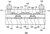
- 2 shows a cross section of an electronic device 200.
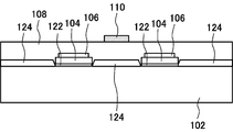
- 2 shows a cross section of the electronic device 200 in the manufacturing process.
- 2 shows a cross section of the electronic device 200 in the manufacturing process.
- 2 shows a cross section of the electronic device 200 in the manufacturing process.
- FIG. 1 shows a cross section of an electronic device 100.
- the electronic device 100 includes a base substrate 102, a group 3-5 compound semiconductor crystal 104, an electronic element 106, an insulating film 108, a passive element 110, an electrode 112, an electrode 113, a coupling wiring 114, a coupling wiring 116, and a coupling wiring 118.
- the surface of the base substrate 102 is a silicon crystal.
- the base substrate 102 is, for example, a silicon wafer or SOI (Silicon on ulator Insulator) whose whole bulk is silicon.
- the group 3-5 compound semiconductor crystal 104 is formed in a partial region on the silicon crystal. That is, the group 3-5 compound semiconductor crystal 104 is locally formed on the silicon crystal. When the group 3-5 compound semiconductor crystal 104 is formed in a partial region on the silicon crystal, the formed group 3-5 compound semiconductor crystal 104 is annealed to eliminate internal crystal defects. Therefore, the crystallinity inside the group 3-5 compound semiconductor crystal 104 is improved.
- the group 3-5 compound semiconductor crystal 104 is, for example, GaAs, AlGaAs, InGaAs, InGaP, GaP, InP, or GaN.
- the electronic device 100 may have a substance other than the group 3-5 compound semiconductor crystal 104 between the silicon crystal and the group 3-5 compound semiconductor crystal 104.
- the electronic element 106 includes a part of the group 3-5 compound semiconductor crystal 104 as an active layer.
- a region that does not become an active layer of the electronic element 106 may function as a buffer layer between the base substrate 102 and the electronic element 106.
- the electronic element 106 is, for example, a field effect transistor, a bipolar transistor, a diode, a light emitting element, or a light receiving element.
- the group 3-5 compound semiconductor crystal 104 and the electronic element 106 are shown as if there is no overlapping portion, but this is omitted for the sake of brevity.
- the electronic device 106 includes a part of the group 3-5 compound semiconductor crystal 104 as an active layer. The same applies to the following drawings.
- the insulating film 108 is formed on the base substrate 102 and covers the electronic element 106.
- the insulating film 108 electrically insulates the electronic element 106 from the electrode 112 and the passive element 110.
- the insulating film 108 is, for example, silicon oxide, silicon nitride, silicon oxynitride, a fluoride thereof, benzocyclobutene resin, a liquid crystal polymer, or polyimide.
- the insulating film 108 covers the electronic element 106 in a region excluding a region where the coupling wiring 114 and the coupling wiring 116 are in contact with the electronic element 106.
- the passive element 110 is formed on the insulating film 108 and is electrically coupled to the electronic element 106 through the coupling wiring 116.
- the passive element 110 is, for example, a resistor, a capacitor, a coil, or a wiring.
- the resistor has a metal thin film or polysilicon.
- the capacitor includes an insulating film and a conductor film that sandwiches the insulating film.
- the coil has a conductor patterned in a coil shape.
- the wiring is, for example, a metal film or a semiconductor such as polysilicon doped with impurities at a high concentration.
- the electrode 112 functions as a terminal that is electrically connected to an external circuit.
- the electrode 112 is formed on the insulating film 108 and is electrically coupled to the electronic element 106 through the coupling wiring 114.
- the electrode 112 is a conductor, and is, for example, a semiconductor doped with a metal such as aluminum, copper, or tungsten, or impurities at a high concentration.
- the coupling wiring 114 penetrates the insulating film 108 and is at least partially formed on the insulating film 108 to electrically couple the electronic element 106 and the electrode 112.
- the bonding wiring 114 starts from the electronic element 106 and is in a direction perpendicular to the surface where the group 3-5 compound semiconductor crystal 104 and the electronic element 106 are in contact, that is, a stack of the group 3-5 compound semiconductor crystal 104 and the electronic element 106. It extends in the direction and penetrates the insulating film 108.
- the coupling wiring 114 is bent above the electronic element 106 and extends along the surface of the insulating film 108 until reaching the electrode 112.
- the coupling wiring 116 penetrates the insulating film 108.
- the coupling wiring 116 is at least partially formed on the insulating film 108, and electrically couples the electronic element 106 and the passive element 110.
- the bonding wiring 116 starts from the electronic element 106 and is in a direction perpendicular to the surface where the group 3-5 compound semiconductor crystal 104 and the electronic element 106 are in contact, that is, a stack of the group 3-5 compound semiconductor crystal 104 and the electronic element 106. It extends in the direction and penetrates the insulating film 108.
- the coupling wiring 116 bends above the electronic element 106 and extends along the surface of the insulating film 108 until reaching the passive element 110.
- the coupling wiring 118 electrically couples the passive element 110 and the electrode 113.
- the coupling wiring 118 is formed on the surface of the insulating film 108 in contact with the passive element 110 and the electrode 113.
- the coupling wiring 114 and the coupling wiring 116 extend in a direction away from the electronic element 106 and extend along the surface of the insulating film 108 in the coupling wiring 114 and the coupling wiring 116, the passive element 110. , And the electrode 112 are formed on the same plane of the insulating film 108. Therefore, even when the electronic element 106 is formed so as to protrude from the surface of the base substrate 102, the coupling wiring 114 and the coupling wiring 116 are on the step between the electronic element 106 and the surface of the base substrate 102. Not formed. As a result, the possibility that the coupling wiring 114 and the coupling wiring 116 are disconnected is low, and the reliability of the electronic device 100 is improved.
- the coupling wiring 114 and the coupling wiring 116 are formed away from the base substrate 102, the coupling wiring 114 and the coupling wiring are compared with the case where the coupling wiring 114 and the coupling wiring 116 are formed on the base substrate 102.
- the stray capacitance of 116 is small. As a result, the operation speed of the electronic device 100 can be increased.
- the passive element 110 is formed on the insulating film 108, the degree of element integration of the electronic device 100 can be increased.
- the coupling wiring 114 and the coupling wiring 116 are connected to the electronic element 106, but other coupling wiring may be connected to the electronic element 106.
- the electronic element 106 is a transistor, the electronic element 106 has at least three coupled wirings.
- FIG. 2 shows a cross section of the electronic device 200.
- the electronic device 200 is a semiconductor wafer formed using, for example, a standard wafer-sized base substrate 102.
- the semiconductor wafer is a substrate having an integrated circuit including a semiconductor thin film.
- the electronic device 200 includes a plurality of group 3-5 compound semiconductor crystals 104 formed in a partial region on the silicon crystal on the surface of the base substrate 102.
- the electronic device 106 includes a part of each of the plurality of Group 3-5 compound semiconductor crystals 104 out of the plurality of Group 3-5 compound semiconductor crystals 104 as an active layer. Includes one by one.
- the part of the plurality of Group 3-5 compound semiconductor crystals 104 are regularly arranged. As an example, some of the plurality of Group 3-5 compound semiconductor crystals 104 are arranged in a periodically repeated arrangement pattern. In each of the periodically repeated arrangement patterns, a plurality of Group 3-5 compound semiconductor crystals 104 are relatively arranged in the same arrangement.
- Some of the plurality of Group 3-5 compound semiconductor crystals 104 may be arranged in a periodic arrangement pattern having rotational symmetry. In other words, the group 3-5 compound semiconductor crystal 104 may be arranged at a position moved at a certain rotation angle on the circumference centered on the reference position on the base substrate 102.
- the plurality of Group 3-5 compound semiconductor crystals 104 are arranged rotated by 180 degrees, 120 degrees, 90 degrees, or 60 degrees.
- the plurality of Group 3-5 compound semiconductor crystals 104 may be arranged rotated by 72 degrees, 45 degrees, 36 degrees, or 30 degrees.
- the plurality of Group 3-5 compound semiconductor crystals 104 may be arranged in a Penrose tile arrangement pattern in which a rhombus having an acute angle of 72 degrees and an obtuse angle of 108 degrees and a rhombus having an acute angle of 36 degrees and an obtuse angle of 144 degrees are combined.
- the plurality of Group 3-5 compound semiconductor crystals 104 are arranged in a lattice pattern.
- the plurality of Group 3-5 compound semiconductor crystals 104 may be arranged at equal intervals.
- the center points as reference positions of the plurality of Group 3-5 compound semiconductor crystals 104 are arranged in a straight line in the first direction, and are also arranged in a straight line in the second direction orthogonal to the first direction. Is done.
- Arranging the plurality of Group 3-5 compound semiconductor crystals 104 in a plurality of periodically repeated arrangement patterns can improve the degree of freedom in the layout design of the Group 3-5 compound semiconductor crystal 104, and allows epitaxial growth. Control of conditions becomes easy.
- the electronic element 106 is formed only on a part of the group 3-5 compound semiconductor crystal 104 among the plurality of group 3-5 compound semiconductor crystals 104, and the electron element 106 is formed on the other group 3-5 compound semiconductor crystal 104.
- the epitaxial growth conditions can be controlled so that the same group of a plurality of electronic elements 106 in which the element 106 is not formed is formed on the base substrate 102.
- the electronic device 200 By cutting the electronic device 200, a plurality of electronic devices having the electronic element 106 can be manufactured. For example, the electronic device 200 is cut at a boundary between periodically arranged arrangement patterns composed of a plurality of electronic elements 106.
- the electronic device 200 has a sealing material 120 formed on the insulating film 108.
- the electrode 112 penetrates the sealing material 120 and is exposed on the surface of the sealing material 120.
- the sealing material 120 is, for example, an epoxy resin, a benzocyclobutene resin, a liquid crystal polymer, and polyimide.
- Ball bumps 126 may be formed on each of the electrodes 112. The ball bump 126 is in contact with the electrode 112 on the surface of the sealing material 120.
- the electronic device 200 may include a seed body 122 between the base substrate 102 and the group 3-5 compound semiconductor crystal 104.
- the seed body 122 relaxes the lattice mismatch between the silicon crystal and the group 3-5 compound semiconductor crystal 104 on the surface of the base substrate 102.
- Examples of the seed body 122 include C x Si y Ge z Sn 1-xyz (0 ⁇ x ⁇ 1, 0 ⁇ y ⁇ 1, 0 ⁇ z ⁇ 1, 0 ⁇ x + y + z ⁇ 1).
- Al a Ga b In 1-ab N c P d As 1-cd (0 ⁇ a ⁇ 1, 0 ⁇ b ⁇ 1) lattice-matched or pseudo-lattice-matched with GaAs , 0 ⁇ c ⁇ 1, 0 ⁇ d ⁇ 1, 0 ⁇ a + b ⁇ 1, 0 ⁇ c + d ⁇ 1).
- the electronic device 200 may include an inhibitor 124 formed on the base substrate 102.
- the inhibitor 124 inhibits the growth of the compound semiconductor crystal.
- the inhibitor 124 has an opening reaching the base substrate 102, and the seed body 122 is formed inside the opening of the inhibitor 124.
- the Group 3-5 compound semiconductor crystal 104 can be selectively epitaxially grown in the opening position.
- the transistor and the passive element 110 may form a microwave circuit.
- the transistor is preferably an EFT (field effect transistor).
- the FET include a heterostructure FET having a GaAs channel, a GaN channel, or an InGaAs channel.
- the transistor may be a heterobipolar transistor.
- the passive element 110 includes a resistor, and the resistor has a ballast function for preventing thermal runaway of the heterobipolar transistor.
- the heterobipolar transistor include a heterobipolar transistor including an InGaP emitter or an AlGaAs emitter, a GaAs base, and a GaAs collector.
- FIG. 3 to 5 show cross sections in the manufacturing process of the electronic device 200.
- FIG. 3 a seed body 122 formed in a partial region on the base substrate 102 whose surface is a silicon crystal, and a group 3-5 compound semiconductor crystal 104 formed on the seed body 122 are formed.
- An electronic element 106 including a part thereof as an active layer is formed on the base substrate 102.
- an insulating film 108 that covers the electronic element 106 is formed.
- the passive element 110 is formed on the insulating film 108.
- an electrode 112 for external connection is formed on the insulating film 108.
- a via hole that penetrates the insulating film 108 and reaches the electronic element 106 is formed in the insulating film 108.
- a via hole corresponding to the coupling wiring 116 that electrically couples the electronic element 106 and the passive element 110 and a via hole corresponding to the coupling wiring 114 that electrically couples the electronic element 106 and the electrode 112 are formed.
- each via hole is filled with a conductor.
- a conductive paste is applied to the via hole on the surface of the insulating film 108 to fill the via hole with a conductor.
- a coupling wiring 114 that electrically couples the electronic element 106 and the passive element 110 and a coupling wiring 116 that electrically couples the electronic element 106 and the electrode 112 via the conductor are formed.
- the coupling wiring 114 and the coupling wiring 116 including the conductor in the via hole may be formed using a dual damascene method.
- the presence of the inhibitor 124 provided to form the group 3-5 compound semiconductor crystal 104 on the base substrate 102 allows the group 3-5 compound semiconductor crystal 104 and the inhibitor 124 to be separated. Even if a gap is generated between them, the coupling wiring is not arranged on the gap. Therefore, it is possible to prevent the coupling wiring from being disconnected due to a step in the gap.
- ball bumps 126 that are in contact with the surface of the sealing material 120 are provided.
- the ball bump 126 is in contact with the surface of the sealing material 120 and is electrically coupled to the electronic element 106 through the electrode 112 and the coupling wiring 116. Since the electronic device 200 has a shape suitable for surface mounting because the ball bumps 126 are provided on the flat surface of the sealing material 120, the electronic device 200 can be used to mount electronic circuits at a high density. become.
Landscapes
- Internal Circuitry In Semiconductor Integrated Circuit Devices (AREA)
- Engineering & Computer Science (AREA)
- Semiconductor Integrated Circuits (AREA)
- Manufacturing & Machinery (AREA)
- Microelectronics & Electronic Packaging (AREA)
- Bipolar Transistors (AREA)
Abstract
Description
(特許文献1)特開2001-68580号公報
Claims (13)
- 表面がシリコン結晶であるベース基板と、
前記シリコン結晶上の一部の領域に形成された3-5族化合物半導体結晶と、
前記3-5族化合物半導体結晶の一部を活性層として含む電子素子と、
前記ベース基板上に形成され、前記電子素子を覆う絶縁膜と、
前記絶縁膜上に形成された電極と、
前記絶縁膜を貫通し、少なくとも一部が前記絶縁膜上に形成され、前記電子素子と前記電極とを電気的に結合する第1の結合配線と、
前記絶縁膜上に形成された受動素子と、
前記絶縁膜を貫通し、少なくとも一部が前記絶縁膜上に形成され、前記電子素子と前記受動素子とを電気的に結合する第2の結合配線と
を備える電子デバイス。 - 前記絶縁膜上に形成され、前記電極及び前記第1の結合配線を封止する封止材をさらに備え、
前記電極は、前記封止材を貫通して前記封止材の表面に露出している
請求項1に記載の電子デバイス。 - 前記3-5族化合物半導体結晶は、前記シリコン結晶と前記3-5族化合物半導体結晶との間の格子不整合を緩和するシード体を介して形成されている
請求項1に記載の電子デバイス。 - 前記シード体は、組成がCxSiyGezSn1-x-y-z(0≦x<1、0≦y≦1、0≦z<1、0<x+y+z≦1)である
請求項3に記載の電子デバイス。 - 前記3-5族化合物半導体結晶は、GaAs結晶、及び前記GaAs結晶に格子整合または擬格子整合するAlaGabIn1-a-bNcPdAs1-c―d(0≦a≦1、0≦b≦1、0≦c≦1、0≦d≦1、0≦a+b≦1、0≦c+d≦1)結晶を含む、
請求項4に記載の電子デバイス。 - 前記ベース基板上に、化合物半導体結晶の成長を阻害する阻害体をさらに備え、
前記シード体は、前記阻害体に形成されかつ前記ベース基板に達する開口内に形成されている
請求項3に記載の電子デバイス。 - 前記電子素子がトランジスタであり、
前記トランジスタと前記受動素子とがマイクロ波回路を形成している
請求項3に記載の電子デバイス。 - 前記トランジスタがFETである
請求項7に記載の電子デバイス。 - 前記トランジスタがヘテロバイポーラトランジスタであり、
前記受動素子が前記ヘテロバイポーラトランジスタの熱暴走を阻止する抵抗体を含む
請求項7に記載の電子デバイス。 - 前記第1の結合配線及び前記第2の結合配線が、前記シード体と前記電子素子とが接する面に垂直な方向に、前記電子素子から延伸している
請求項3に記載の電子デバイス。 - 表面がシリコン結晶であるベース基板と、
前記シリコン結晶上の一部の領域に形成された複数の3-5族化合物半導体結晶と、
前記複数の3-5族化合物半導体結晶のうち一部の複数の3-5族化合物半導体結晶のそれぞれの3-5族化合物半導体結晶の一部を活性層としてそれぞれ1つずつ含む電子素子と、
前記ベース基板上に形成され、前記電子素子を覆う絶縁膜と、
前記絶縁膜上に形成された電極と、
前記絶縁膜を貫通し、少なくとも一部が前記絶縁膜上に形成され、前記電子素子と前記電極とを電気的に結合する第1の結合配線と、
前記絶縁膜上に形成された受動素子と、
前記絶縁膜を貫通し、少なくとも一部が前記絶縁膜上に形成され、前記電子素子と前記受動素子とを電気的に結合する第2の結合配線と
を備え、
前記一部の複数の3-5族化合物半導体結晶は、規則的に配置されている
半導体ウエハー。 - 表面がシリコン結晶であるベース基板と、
前記シリコン結晶上の一部の領域に形成された複数のシード体と、
前記複数のシード体のそれぞれのシード体上に形成された複数の3-5族化合物半導体結晶と、
前記複数の3-5族化合物半導体結晶のうち一部の複数の3-5族化合物半導体結晶のそれぞれの3-5族化合物半導体結晶の一部を活性層としてそれぞれ1つずつ含む電子素子と、
前記ベース基板上に形成され、前記電子素子を覆う絶縁膜と、
前記絶縁膜上に形成された電極と、
前記絶縁膜を貫通し、少なくとも一部が前記絶縁膜上に形成され、前記電子素子と前記電極とを電気的に結合する第1の結合配線と、
前記絶縁膜上に形成された受動素子と、
前記絶縁膜を貫通し、少なくとも一部が前記絶縁膜上に形成され、前記電子素子と前記受動素子とを電気的に結合する第2の結合配線と
を備え、
前記シード体は、前記シリコン結晶と前記3-5族化合物半導体結晶との間の格子不整合を緩和する結晶であり、
前記複数のシード体は、規則的に配置されている
半導体ウエハー。 - 表面がシリコン結晶であるベース基板上の一部の領域に形成されたシード体と、前記シード体上に形成され、活性層として機能する層を含む3-5族化合物半導体結晶を有する電子素子とを備える基体に、
前記電子素子を覆う絶縁膜を形成する段階と、
前記絶縁膜上に、前記電子素子と電気的に結合される電極を形成する段階と、
前記絶縁膜上に、前記電子素子と電気的に結合される受動素子を形成する段階と、
前記電子素子に達する第1のビアホール及び第2のビアホールを前記絶縁膜に形成する段階と、
前記第1のビアホールを介して前記電子素子と前記電極とを電気的に結合する第1の結合配線を形成する段階と、
前記第2のビアホールを介して前記電子素子と前記受動素子とを電気的に結合する第2の結合配線を形成する段階と
を備える電子デバイスの製造方法。
Priority Applications (3)
| Application Number | Priority Date | Filing Date | Title |
|---|---|---|---|
| CN2011800069406A CN102714176A (zh) | 2010-02-26 | 2011-02-22 | 电子器件及电子器件的制造方法 |
| KR1020127018971A KR20120127419A (ko) | 2010-02-26 | 2011-02-22 | 전자 디바이스 및 전자 디바이스의 제조 방법 |
| US13/594,442 US8878250B2 (en) | 2010-02-26 | 2012-08-24 | Electronic device and method for producing electronic device |
Applications Claiming Priority (2)
| Application Number | Priority Date | Filing Date | Title |
|---|---|---|---|
| JP2010-042609 | 2010-02-26 | ||
| JP2010042609 | 2010-02-26 |
Related Child Applications (1)
| Application Number | Title | Priority Date | Filing Date |
|---|---|---|---|
| US13/594,442 Continuation-In-Part US8878250B2 (en) | 2010-02-26 | 2012-08-24 | Electronic device and method for producing electronic device |
Publications (1)
| Publication Number | Publication Date |
|---|---|
| WO2011105056A1 true WO2011105056A1 (ja) | 2011-09-01 |
Family
ID=44506487
Family Applications (1)
| Application Number | Title | Priority Date | Filing Date |
|---|---|---|---|
| PCT/JP2011/000991 Ceased WO2011105056A1 (ja) | 2010-02-26 | 2011-02-22 | 電子デバイスおよび電子デバイスの製造方法 |
Country Status (6)
| Country | Link |
|---|---|
| US (1) | US8878250B2 (ja) |
| JP (1) | JP2011199267A (ja) |
| KR (1) | KR20120127419A (ja) |
| CN (1) | CN102714176A (ja) |
| TW (1) | TW201201356A (ja) |
| WO (1) | WO2011105056A1 (ja) |
Families Citing this family (6)
| Publication number | Priority date | Publication date | Assignee | Title |
|---|---|---|---|---|
| CN103811364B (zh) * | 2013-12-26 | 2017-03-29 | 中国电子科技集团公司第五十五研究所 | 一种实现基于bcb的磷化铟微波电路多层互联方法 |
| US10593600B2 (en) | 2016-02-24 | 2020-03-17 | International Business Machines Corporation | Distinct gate stacks for III-V-based CMOS circuits comprising a channel cap |
| US10062693B2 (en) * | 2016-02-24 | 2018-08-28 | International Business Machines Corporation | Patterned gate dielectrics for III-V-based CMOS circuits |
| KR102787780B1 (ko) | 2018-12-24 | 2025-03-27 | 삼성디스플레이 주식회사 | 유기 발광 표시 장치 및 그 제조 방법 |
| JP7516786B2 (ja) * | 2019-06-21 | 2024-07-17 | 株式会社村田製作所 | 半導体装置及びその製造方法 |
| CN111900093A (zh) * | 2020-07-14 | 2020-11-06 | 南京中电芯谷高频器件产业技术研究院有限公司 | 一种bcb薄膜太赫兹电路及其制作方法 |
Citations (9)
| Publication number | Priority date | Publication date | Assignee | Title |
|---|---|---|---|---|
| JPS60257162A (ja) * | 1984-06-01 | 1985-12-18 | Nec Corp | GaAs半導体集積回路 |
| JPS6318661A (ja) * | 1986-06-13 | 1988-01-26 | マサチュ−セッツ・インステチュ−ト・オブ・テクノロジ− | 化合物半導体の製造方法および半導体回路 |
| JPH0513584A (ja) * | 1991-07-03 | 1993-01-22 | Matsushita Electric Ind Co Ltd | 半導体装置およびその製造方法 |
| JPH06232126A (ja) * | 1993-02-03 | 1994-08-19 | Nippon Telegr & Teleph Corp <Ntt> | 複合半導体回路装置およびその作製方法 |
| JP2002093920A (ja) * | 2000-06-27 | 2002-03-29 | Matsushita Electric Ind Co Ltd | 半導体デバイス |
| JP2003234411A (ja) * | 2001-12-07 | 2003-08-22 | Taiyo Yuden Co Ltd | 高周波モジュールおよびその製造方法 |
| JP2009177168A (ja) * | 2007-12-28 | 2009-08-06 | Sumitomo Chemical Co Ltd | 半導体基板、半導体基板の製造方法および電子デバイス |
| JP2009177167A (ja) * | 2007-12-28 | 2009-08-06 | Sumitomo Chemical Co Ltd | 半導体基板、半導体基板の製造方法および電子デバイス |
| JP2010021583A (ja) * | 2008-03-01 | 2010-01-28 | Sumitomo Chemical Co Ltd | 半導体基板、半導体基板の製造方法および電子デバイス |
Family Cites Families (12)
| Publication number | Priority date | Publication date | Assignee | Title |
|---|---|---|---|---|
| JP2953966B2 (ja) * | 1994-10-14 | 1999-09-27 | 日本電気株式会社 | バイポーラトランジスタの製造方法 |
| JPH10289979A (ja) * | 1997-04-15 | 1998-10-27 | Nippon Steel Corp | 高周波半導体デバイス |
| US6265246B1 (en) | 1999-07-23 | 2001-07-24 | Agilent Technologies, Inc. | Microcap wafer-level package |
| WO2002001641A1 (en) * | 2000-06-27 | 2002-01-03 | Matsushita Electric Industrial Co., Ltd. | Semiconductor device |
| US6815796B2 (en) | 2001-12-07 | 2004-11-09 | Taiyo Yuden Co., Ltd. | Composite module and process of producing same |
| JP2004241471A (ja) * | 2003-02-04 | 2004-08-26 | Renesas Technology Corp | 化合物半導体装置とその製造方法、半導体装置及び高周波モジュール |
| CN101156162B (zh) * | 2005-03-31 | 2012-05-16 | 株式会社半导体能源研究所 | 无线芯片以及具有无线芯片的电子设备 |
| JP2008181990A (ja) * | 2007-01-24 | 2008-08-07 | Sony Corp | 半導体装置の製造方法および半導体装置 |
| JP5669359B2 (ja) * | 2008-03-01 | 2015-02-12 | 住友化学株式会社 | 半導体基板、半導体基板の製造方法および電子デバイス |
| US8823141B2 (en) * | 2009-03-11 | 2014-09-02 | Sumitomo Chemical Company, Limited | Semiconductor wafer, method of producing semiconductor wafer, electronic device, and method of producing electronic device |
| KR20120022872A (ko) * | 2009-05-22 | 2012-03-12 | 스미또모 가가꾸 가부시키가이샤 | 반도체 기판, 전자 디바이스, 반도체 기판의 제조 방법 및 전자 디바이스의 제조 방법 |
| JP2011199268A (ja) * | 2010-02-26 | 2011-10-06 | Sumitomo Chemical Co Ltd | 半導体基板、半導体デバイスおよび半導体基板の製造方法 |
-
2011
- 2011-02-22 KR KR1020127018971A patent/KR20120127419A/ko not_active Withdrawn
- 2011-02-22 JP JP2011036186A patent/JP2011199267A/ja active Pending
- 2011-02-22 CN CN2011800069406A patent/CN102714176A/zh active Pending
- 2011-02-22 WO PCT/JP2011/000991 patent/WO2011105056A1/ja not_active Ceased
- 2011-02-25 TW TW100106353A patent/TW201201356A/zh unknown
-
2012
- 2012-08-24 US US13/594,442 patent/US8878250B2/en not_active Expired - Fee Related
Patent Citations (9)
| Publication number | Priority date | Publication date | Assignee | Title |
|---|---|---|---|---|
| JPS60257162A (ja) * | 1984-06-01 | 1985-12-18 | Nec Corp | GaAs半導体集積回路 |
| JPS6318661A (ja) * | 1986-06-13 | 1988-01-26 | マサチュ−セッツ・インステチュ−ト・オブ・テクノロジ− | 化合物半導体の製造方法および半導体回路 |
| JPH0513584A (ja) * | 1991-07-03 | 1993-01-22 | Matsushita Electric Ind Co Ltd | 半導体装置およびその製造方法 |
| JPH06232126A (ja) * | 1993-02-03 | 1994-08-19 | Nippon Telegr & Teleph Corp <Ntt> | 複合半導体回路装置およびその作製方法 |
| JP2002093920A (ja) * | 2000-06-27 | 2002-03-29 | Matsushita Electric Ind Co Ltd | 半導体デバイス |
| JP2003234411A (ja) * | 2001-12-07 | 2003-08-22 | Taiyo Yuden Co Ltd | 高周波モジュールおよびその製造方法 |
| JP2009177168A (ja) * | 2007-12-28 | 2009-08-06 | Sumitomo Chemical Co Ltd | 半導体基板、半導体基板の製造方法および電子デバイス |
| JP2009177167A (ja) * | 2007-12-28 | 2009-08-06 | Sumitomo Chemical Co Ltd | 半導体基板、半導体基板の製造方法および電子デバイス |
| JP2010021583A (ja) * | 2008-03-01 | 2010-01-28 | Sumitomo Chemical Co Ltd | 半導体基板、半導体基板の製造方法および電子デバイス |
Also Published As
| Publication number | Publication date |
|---|---|
| US20120319170A1 (en) | 2012-12-20 |
| KR20120127419A (ko) | 2012-11-21 |
| US8878250B2 (en) | 2014-11-04 |
| JP2011199267A (ja) | 2011-10-06 |
| CN102714176A (zh) | 2012-10-03 |
| TW201201356A (en) | 2012-01-01 |
Similar Documents
| Publication | Publication Date | Title |
|---|---|---|
| US12211839B2 (en) | Nitride semiconductor device | |
| JP5650686B2 (ja) | パッケージ支持面にクリップを利用する高電圧iii族窒化物整流器パッケージ | |
| US20090194792A1 (en) | Semiconductor device and manufacturing method therefor | |
| US20150084103A1 (en) | Semiconductor device and method for manufacturing the same | |
| WO2011105056A1 (ja) | 電子デバイスおよび電子デバイスの製造方法 | |
| US11728419B2 (en) | High electron mobility transistor | |
| JP5711180B2 (ja) | エッチングリードフレームを備えるカスコード接続された高電圧iii族窒化物整流器パッケージ及びその製造方法 | |
| JP4492034B2 (ja) | Hemt及びその製造方法 | |
| US10985084B2 (en) | Integrated III-V device and driver device packages with improved heat removal and methods for fabricating the same | |
| US20150021666A1 (en) | Transistor having partially or wholly replaced substrate and method of making the same | |
| US10068780B2 (en) | Lead frame connected with heterojunction semiconductor body | |
| CN1706033A (zh) | 薄膜晶体晶片的制造方法、使用该晶片的半导体器件及其制造方法 | |
| CN119767686B (zh) | 电阻器及其制备方法、集成电路、电子设备 | |
| US20250300151A1 (en) | Semiconductor device, semiconductor module, and method for manufacturing semiconductor device | |
| CN112802802B (zh) | 基于su-8光阻胶的半导体功率器件及其制备方法和包括其的功率模块 | |
| US12262556B2 (en) | Power amplifier | |
| US11588036B2 (en) | High-efficiency packaged chip structure and electronic device including the same | |
| CN116936509A (zh) | 半导体装置及其制造方法 | |
| US20240194561A1 (en) | Hetero-junction bipolar transistor and method of manufacturing the same | |
| CN120529635A (zh) | 半导体器件及芯片 | |
| CN120435029A (zh) | 半导体器件及制备方法、封装结构、电子设备 | |
| CN119730298A (zh) | 半导体器件及其制备方法、芯片、电子设备 | |
| TW202512263A (zh) | 半導體結構及其形成方法 | |
| CN120166734A (zh) | 蓝宝石GaN HEMT功率芯片的制作方法 | |
| WO2021240990A1 (ja) | 半導体装置、半導体モジュール、及び電子機器 |
Legal Events
| Date | Code | Title | Description |
|---|---|---|---|
| WWE | Wipo information: entry into national phase |
Ref document number: 201180006940.6 Country of ref document: CN |
|
| 121 | Ep: the epo has been informed by wipo that ep was designated in this application |
Ref document number: 11747026 Country of ref document: EP Kind code of ref document: A1 |
|
| ENP | Entry into the national phase |
Ref document number: 20127018971 Country of ref document: KR Kind code of ref document: A |
|
| NENP | Non-entry into the national phase |
Ref country code: DE |
|
| 122 | Ep: pct application non-entry in european phase |
Ref document number: 11747026 Country of ref document: EP Kind code of ref document: A1 |