WO2011055822A1 - 基板処理装置、基板搬送装置及び基板処理装置の制御方法 - Google Patents
基板処理装置、基板搬送装置及び基板処理装置の制御方法 Download PDFInfo
- Publication number
- WO2011055822A1 WO2011055822A1 PCT/JP2010/069849 JP2010069849W WO2011055822A1 WO 2011055822 A1 WO2011055822 A1 WO 2011055822A1 JP 2010069849 W JP2010069849 W JP 2010069849W WO 2011055822 A1 WO2011055822 A1 WO 2011055822A1
- Authority
- WO
- WIPO (PCT)
- Prior art keywords
- substrate
- transfer arm
- electrostatic chuck
- electrodes
- time
- Prior art date
- Legal status (The legal status is an assumption and is not a legal conclusion. Google has not performed a legal analysis and makes no representation as to the accuracy of the status listed.)
- Ceased
Links
Images






Classifications
-
- H—ELECTRICITY
- H10—SEMICONDUCTOR DEVICES; ELECTRIC SOLID-STATE DEVICES NOT OTHERWISE PROVIDED FOR
- H10P—GENERIC PROCESSES OR APPARATUS FOR THE MANUFACTURE OR TREATMENT OF DEVICES COVERED BY CLASS H10
- H10P72/00—Handling or holding of wafers, substrates or devices during manufacture or treatment thereof
- H10P72/30—Handling or holding of wafers, substrates or devices during manufacture or treatment thereof for conveying, e.g. between different workstations
- H10P72/33—Handling or holding of wafers, substrates or devices during manufacture or treatment thereof for conveying, e.g. between different workstations into and out of processing chamber
-
- H—ELECTRICITY
- H10—SEMICONDUCTOR DEVICES; ELECTRIC SOLID-STATE DEVICES NOT OTHERWISE PROVIDED FOR
- H10P—GENERIC PROCESSES OR APPARATUS FOR THE MANUFACTURE OR TREATMENT OF DEVICES COVERED BY CLASS H10
- H10P72/00—Handling or holding of wafers, substrates or devices during manufacture or treatment thereof
- H10P72/70—Handling or holding of wafers, substrates or devices during manufacture or treatment thereof for supporting or gripping
- H10P72/72—Handling or holding of wafers, substrates or devices during manufacture or treatment thereof for supporting or gripping using electrostatic chucks
- H10P72/722—Details of electrostatic chucks
-
- H—ELECTRICITY
- H10—SEMICONDUCTOR DEVICES; ELECTRIC SOLID-STATE DEVICES NOT OTHERWISE PROVIDED FOR
- H10P—GENERIC PROCESSES OR APPARATUS FOR THE MANUFACTURE OR TREATMENT OF DEVICES COVERED BY CLASS H10
- H10P72/00—Handling or holding of wafers, substrates or devices during manufacture or treatment thereof
- H10P72/30—Handling or holding of wafers, substrates or devices during manufacture or treatment thereof for conveying, e.g. between different workstations
- H10P72/33—Handling or holding of wafers, substrates or devices during manufacture or treatment thereof for conveying, e.g. between different workstations into and out of processing chamber
- H10P72/3302—Mechanical parts of transfer devices
-
- H—ELECTRICITY
- H10—SEMICONDUCTOR DEVICES; ELECTRIC SOLID-STATE DEVICES NOT OTHERWISE PROVIDED FOR
- H10P—GENERIC PROCESSES OR APPARATUS FOR THE MANUFACTURE OR TREATMENT OF DEVICES COVERED BY CLASS H10
- H10P72/00—Handling or holding of wafers, substrates or devices during manufacture or treatment thereof
- H10P72/70—Handling or holding of wafers, substrates or devices during manufacture or treatment thereof for supporting or gripping
- H10P72/76—Handling or holding of wafers, substrates or devices during manufacture or treatment thereof for supporting or gripping using mechanical means, e.g. clamps or pinches
- H10P72/7602—Handling or holding of wafers, substrates or devices during manufacture or treatment thereof for supporting or gripping using mechanical means, e.g. clamps or pinches the wafers being placed on a robot blade or gripped by a gripper for conveyance
Definitions
- the present invention relates to a substrate processing apparatus, a substrate transfer apparatus, and a method for controlling the substrate processing apparatus.
- a substrate processing apparatus As a manufacturing apparatus for manufacturing such a semiconductor device, there is a substrate processing apparatus called a cluster tool.
- a substrate processing apparatus a plurality of single-wafer processing chambers for performing various processes and a single transfer chamber are connected, and processing on semiconductor wafers is sequentially performed in each processing chamber, whereby one substrate processing is performed.
- the apparatus can perform various processes.
- the movement of the semiconductor wafer between the processing chambers is performed by an expansion / contraction operation and a rotation operation of a transfer arm provided in the transfer chamber.
- This transfer arm usually has an electrostatic chuck, and the semiconductor wafer is sucked and transferred by the electrostatic chuck of the transfer arm.
- the semiconductor wafer moves between the processing chambers, it is in a state of being attracted to the electrostatic chuck on the transfer arm by applying a voltage to the electrode of the electrostatic chuck.
- the semiconductor wafer is not easily separated from the transfer arm, and over-adsorption may occur. Therefore, there is a demand for a substrate processing apparatus having a transfer arm that is unlikely to cause excessive adsorption, a substrate transfer apparatus, and a method for controlling the substrate processing apparatus.
- an electrostatic chuck capable of placing the substrate and attracting the placed substrate, and transporting the substrate, and the substrate on the transport arm.
- a substrate processing apparatus includes a control unit that applies the voltage between the electrodes.
- the substrate can be placed, the electrostatic chuck that attracts the placed substrate, and an expansion and contraction operation and a rotation operation are possible for transporting the substrate.
- a voltage for attracting the substrate to the electrostatic chuck is set to
- the substrate is placed on the transfer arm without applying between the electrodes of the electrostatic chuck, and when the transfer arm is rotating, the voltage is applied between the electrodes.
- a method for controlling a substrate processing apparatus comprising: an electrostatic chuck that can place the substrate, and that attracts the placed substrate, and includes a transport arm that transports the substrate.
- the substrate is placed on the transfer arm, and a voltage is applied between the electrodes of the electrostatic chuck of the transfer arm to attract the substrate to the transfer arm.
- a method for controlling a substrate processing apparatus comprising: an electrostatic chuck that can place the substrate, and that attracts the placed substrate, and includes a transport arm that transports the substrate.
- the control method includes a step of placing the substrate on the transfer arm, and a first movement step of moving the substrate by expanding and contracting the transfer arm without causing the electrostatic chuck to attract the substrate. After the first moving step, the substrate is attracted to the transfer arm by applying a voltage between the electrodes of the electrostatic chuck of the transfer arm, and the transfer arm rotates without expanding and contracting.
- FIG. 1 is a configuration diagram of a substrate processing apparatus according to a first embodiment.
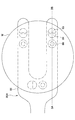
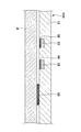
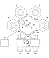
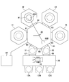
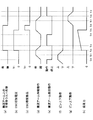
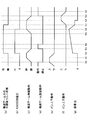
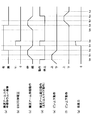
- Top view of transfer arm Cross-sectional enlarged view of transfer arm Timing chart of control method of comparative example in substrate processing apparatus (1) Timing chart of control method of substrate processing apparatus in first embodiment Explanatory drawing (1) of the control method in the substrate processing apparatus in 1st Embodiment Explanatory drawing (2) of the control method in the substrate processing apparatus in 1st Embodiment Explanatory drawing (3) of the control method in the substrate processing apparatus in 1st Embodiment Timing chart of control method of comparative example in substrate processing apparatus (2) Timing chart of control method of substrate processing apparatus in second embodiment Timing chart of control method of comparative example in substrate processing apparatus (3) Timing chart of control method of substrate processing apparatus in third embodiment Timing chart of control method of substrate processing apparatus in fourth embodiment Timing chart of control method of substrate processing apparatus in fifth embodiment
- a substrate processing apparatus having a transfer arm capable of adsorbing a semiconductor wafer by an electrostatic chuck, a substrate processing apparatus and a substrate transfer that can prevent over-adsorption and sticking as much as possible.
- An apparatus and a method for controlling the substrate processing apparatus can be provided. As a result, the wafer can be easily peeled off from the transfer arm, and damage to the device can be prevented.
- the substrate processing apparatus it is possible to provide a substrate processing apparatus, a substrate transport apparatus, and a substrate processing apparatus control method capable of improving throughput and saving power when operating the substrate processing apparatus. That is, the voltage application time to the electrostatic chuck of the transfer arm can be shortened, and power can be saved. Further, there is a case where application of a reverse voltage is not necessary, and further power saving can be achieved.
- This embodiment is a substrate processing apparatus called a cluster tool, that is, a substrate processing apparatus for processing a substrate such as a semiconductor wafer having a plurality of processing chambers and a transfer chamber connected to the plurality of processing chambers.
- the transfer chamber is provided with a transfer arm for adsorbing a semiconductor wafer by an electrostatic chuck (ESC: Electrostatic Chuck), and the substrate between the processing chambers or between the process chamber and the load lock chamber by the transfer arm.
- ESC Electrostatic Chuck
- the substrate processing apparatus in the present embodiment will be described with reference to FIG.
- the substrate processing apparatus in the present embodiment includes an atmospheric transfer chamber 10, a common transfer chamber 20, four single wafer processing chambers 41, 42, 43, 44, and a control unit 50.
- the atmospheric transfer chamber 10 and the common transfer chamber 20 have a function as a substrate transfer device, and the atmospheric transfer chamber 10 and the common transfer chamber 20 are also referred to as substrate transfer devices.
- the common transfer chamber 20 has a substantially hexagonal shape, and four processing chambers 41, 42, 43, and 44 are connected to a portion corresponding to the side of the substantially hexagonal shape.
- Two load lock chambers 31 and 32 are provided between the common transfer chamber 20 and the atmospheric transfer chamber 10.
- Gate valves 61, 62, 63, and 64 are provided between the common transfer chamber 20 and the processing chambers 41, 42, 43, and 44, respectively.
- the common transfer chamber 20 can be shut off.
- gate valves 65 and 66 are provided between the common transfer chamber 20 and the load lock chambers 31 and 32, respectively, and between the load lock chambers 31 and 32 and the atmospheric transfer chamber 10.
- a vacuum pump (not shown) is connected to the common transfer chamber 20 and can be evacuated
- a vacuum pump (not shown) is connected to the load lock chambers 31 and 32 and can be evacuated independently. It is.
- a loading-side transfer mechanism 16 having two transfer arms 16 ⁇ / b> A and 16 ⁇ / b> B is provided to hold the semiconductor wafer W, and the transfer arms 16 ⁇ / b> A and 16 ⁇ / b> B extend, rotate, move up and down, move linearly, and the like.
- the semiconductor wafer W stored in the cassette at the introduction ports 12A, 12B, and 12C can be taken out and moved to one of the load lock chambers 31 and 32.
- a transfer mechanism 80 having two transfer arms 80A and 80B for holding the semiconductor wafer W is provided, and the transfer arm 80A or 80B performs an expansion / contraction operation, a rotation operation, and the like.
- the movement of the semiconductor wafer W between the processing chambers 41, 42, 43, 44, the movement from the inside of the load lock chamber 31 or 32 to the processing chambers 41, 42, 43, 44, the respective processing chambers 41, 42. , 43, 44 can be moved into the load lock chamber 31 or 32.
- the semiconductor wafers W can be moved from the load lock chamber 31 or 32 to the respective processing chambers 41, 42, 43, 44 by the transfer arms 80A and 80B, and the respective processing chambers 41, 42, In 43 and 44, the semiconductor wafer W is processed.
- the processing chambers 41, 42, 43, 44 the processing of the semiconductor wafer W is performed individually. Therefore, the semiconductor wafer W is moved between the processing chambers 41, 42, 43, 44 by the transfer arms 80 ⁇ / b> A and 80 ⁇ / b> B. Processing is performed.
- the semiconductor wafer W is transferred from the processing chamber 41, 42, 43, 44 to the load lock chamber 31 or 32 by the transfer arm 80A or 80B. Further, the semiconductor wafer W after the substrate processing is accommodated in the cassette at the transfer ports 12A, 12B, and 12C by the transfer arm 16A or 16B of the transfer-side transfer mechanism 16 in the atmospheric transfer chamber 10.
- the semiconductor wafer W is placed on the transfer arm 80A or 80B.
- the semiconductor wafer W is placed on the transfer arm 80A or 80B and is not attracted by the electrostatic chuck, it is placed by gravity.
- the operation of the transfer arm 16A or 16B in the transfer-side transfer mechanism 16, the transfer arms 80A and 80B in the transfer mechanism 80, the processing of semiconductor wafers in the processing chambers 41, 42, 43, and 44, the gate valves 61, 62, 63, and 64. , 65, 66, 67, 68, the exhaust of the load lock chamber 31 or 32, etc. are controlled by the control unit 50.
- voltage application between the electrostatic chuck electrodes 82 and 83 (described later) for adsorption by the electrostatic chuck is also controlled by the control unit 50.
- the relationship (timing) between the voltage application controlled by the control unit 50 and the operations of the transfer arms 80A and 80B will be described later.
- the transfer arm 80A in the present embodiment will be described.
- 3 is an enlarged cross-sectional view taken along broken line 3A-3B in FIG.
- the transfer arm 80A has a U-shaped tip portion on which the bifurcated semiconductor wafer W is placed.
- the main body 81 of the transfer arm 80A is made of a ceramic material such as aluminum oxide, and has a U-shaped tip portion on which the semiconductor wafer W is placed.
- the U-shaped tip portion has electrodes 82 and 83 formed of a metal material for performing electrostatic chucking, and an insulating layer 84 made of polyimide or the like is formed on the surfaces of the electrodes 82 and 83. And 85 are formed.
- an O-ring 86 made of silicon rubber containing a silicon compound is provided on the suction surface side of the main body 81 of the main body 81 in the transfer arm 80A, and the semiconductor wafer W is in direct contact with the main body 81. It is configured not to do.
- the transfer arm 80B and the transfer arms 16A and 16B in the transfer-side transfer mechanism 16 are configured in the same manner.
- FIG. 4A shows whether or not a semiconductor wafer is present on the transfer arm
- FIG. 4B shows the voltage applied between the electrodes of the electrostatic chuck.
- 4 (c) shows the operating state of the transfer arm, that is, whether the transfer arm is operating or stopped.
- FIG. 4 (d) shows the state of the transfer arm and the semiconductor wafer by the electrostatic chuck. It shows the adsorption power.
- the transfer arm sucks the semiconductor wafer by the electrostatic chuck. Specifically, after the gate valve between the processing chamber on which the semiconductor wafer is placed and the common transfer chamber is opened and the U-shaped tip of the transfer arm is inserted into the lower portion of the semiconductor wafer, the transfer arm is A voltage V ⁇ b> 1 for attracting between the electrodes of the electrostatic chuck provided on the electrode is applied. As a result, the semiconductor wafer is attracted to the transfer arm. Therefore, at time t0, the semiconductor wafer is attracted to the transfer arm, and the semiconductor wafer is placed on the transfer arm.
- the transfer arm performs an expansion / contraction operation and a rotation operation. Specifically, as the transfer arm contracts, the semiconductor wafer placed at the U-shaped tip of the transfer arm moves from the processing chamber to the common transfer chamber. Thereafter, by rotation, the semiconductor wafer moves to the vicinity of the next processing chamber in which the semiconductor wafer is not placed in the common transfer chamber.
- the transfer arm performs an expansion / contraction operation. Specifically, when the transfer arm is extended, the semiconductor wafer placed at the U-shaped tip portion of the transfer arm moves from the common transfer chamber to the processing chamber.
- a semiconductor wafer is mounted at a predetermined position in the next processing chamber. That is, after the semiconductor wafer is moved to a predetermined position, the voltage applied between the electrodes of the electrostatic chuck is set to 0 V at time t3, so that the attracting force by the electrostatic chuck is released, and the inside of the next processing chamber is released. A semiconductor wafer is placed at a predetermined position.
- the semiconductor wafer may come into close contact with the semiconductor ring via the O-ring. It is not easy to release.
- FIG. 5A shows whether or not the semiconductor wafer W is present on the transfer arm 80A
- FIG. 5B shows the voltage applied between the electrodes 82 and 83 of the electrostatic chuck
- FIG. 5C shows the operating state of the transfer arm 80A, that is, the state where the transfer arm 80A is operating or stopped, and FIG. The suction force between the transfer arm 80A and the semiconductor wafer W by the electric chuck is shown.
- the semiconductor wafer W is attracted by an electrostatic chuck.
- the gate valve 61 between the processing chamber 41 on which the semiconductor wafer W is placed and the common transfer chamber 20 is opened, and the U-shaped tip portion of the transfer arm 80A is After being inserted into the lower part of the semiconductor wafer W, a voltage V1 for attracting the semiconductor wafer W by the electrostatic chuck is applied between the electrodes 82 and 83 of the electrostatic chuck provided on the transfer arm 80A.
- the semiconductor wafer W is attracted to the electrostatic chuck. Therefore, at time t0, the semiconductor wafer W is attracted to the transfer arm 80A.
- the transfer arm 80A performs an expansion / contraction operation and a rotation (turning) operation (first movement step and rotation step). Specifically, when the transfer arm 80 ⁇ / b> A contracts, the semiconductor wafer W placed at the U-shaped tip portion of the transfer arm 80 moves from the processing chamber 81 into the common transfer chamber 20. Thereafter, as shown in FIG. 7, the semiconductor wafer W is moved to the vicinity of the next processing chamber 42 in which the semiconductor wafer W is not placed in the common transfer chamber 20 by performing a rotation operation.
- the transfer arm 80A performs an expansion / contraction operation. Specifically, when the transfer arm 80A is extended, the semiconductor wafer W placed at the U-shaped tip portion of the transfer arm 80A moves from the common transfer chamber 20 into the processing chamber 42. At this time, the voltage V1 is again applied between the electrodes 82 and 83 in the transfer arm 80A, and the semiconductor wafer W is attracted to the transfer arm 80A (second movement step).
- the semiconductor wafer W is placed at a predetermined position in the next processing chamber 42. That is, as shown in FIG. 8, after the semiconductor wafer is moved to a predetermined position for a time t3, the voltage applied between the electrodes of the electrostatic chuck is set to 0 V, so that the adsorption by the electrostatic chuck is released. The semiconductor wafer W is placed at a predetermined position in the next processing chamber 42.
- the semiconductor wafer W can be moved between the processing chambers in the substrate processing apparatus according to the present embodiment.
- the voltage is applied between the electrodes 82 and 83 except for the time when the transfer arm 80A is operating, that is, from time t0 to time t1, and from time t2 to time t3.
- the voltage is 0V.
- the suction by the electrostatic chuck is released, and the excessive suction between the transfer arm 80A and the semiconductor wafer W can be prevented.
- the voltage V1 is not applied between the electrodes 82 and 83 during the time when the transfer arm 80A is not operating, that is, from the time t1 to the time t2, power is not consumed during this time, so that power saving is achieved. It is possible to reduce the cost.
- the present embodiment is a control method for a substrate processing apparatus in the substrate processing apparatus according to the first embodiment, in which the adsorption force due to the residual charge of the electrostatic chuck is removed.
- FIG. 9A shows whether or not a semiconductor wafer is present on the transfer arm
- FIG. 9B is applied between the electrodes of the electrostatic chuck to attract the electrostatic chuck
- FIG. 9C shows the voltage application state
- FIG. 9C shows the voltage application state applied between the electrodes of the electrostatic chuck in order to remove the residual adhesion due to the electrostatic chuck.
- D shows the state of the transfer arm, that is, whether the transfer arm is extended or contracted
- FIG. 9 (e) shows whether or not the transfer arm is rotating.
- FIG. 9F shows the vertical positions of pins for raising and lowering the semiconductor wafer in the processing chamber (hereinafter referred to as “processing chamber A”) in which the semiconductor wafer is first placed.
- FIG. 9G shows a process in which a semiconductor wafer is placed next.
- FIG. 9H shows the vertical position of the pins for moving the semiconductor wafer up and down in the chamber (hereinafter referred to as “processing chamber B”). FIG. It is shown.
- the transfer arm extends toward the processing chamber A where the semiconductor wafer is first placed. At this time, no semiconductor wafer is placed on the transfer arm, and no voltage is applied between the electrodes of the electrostatic chuck of the transfer arm. In the processing chamber A, the pins for lifting the semiconductor wafer are already raised in the processing chamber A, and the semiconductor wafer is in a lifted state. Therefore, at time t11, the transfer arm is in an extended state, and the U-shaped tip end portion of the transfer arm enters the processing chamber A below the semiconductor wafer.
- a voltage V1 for attracting by the electrostatic chuck is applied between the electrodes of the electrostatic chuck provided on the transport arm, whereby the semiconductor wafer is applied to the electrostatic chuck of the transport arm.
- the semiconductor wafer is moved from the processing chamber A to the common transfer chamber by the operation of being attracted and further contracting the transfer arm.
- the transfer arm performs a rotating operation to move the semiconductor wafer to the vicinity of the processing chamber B.
- the transfer arm moves toward the inside of the processing chamber B by moving the semiconductor wafer into the processing chamber B.
- the voltage V1 applied between the electrodes of the electrostatic chuck of the transfer arm at time t15 is turned off, and the voltage applied between the electrodes from time t12 to time t15 from time t15 to time t16 Applies a reverse voltage V2 between the electrodes, thereby removing the charge remaining on the semiconductor wafer and the electrostatic chuck in the transfer arm and reliably releasing the attracting force.
- the pins for lifting the semiconductor wafer in the processing chamber B are raised, and the semiconductor wafer placed on the transfer arm is lifted.
- the transfer arm moves the U-shaped tip from the processing chamber B to the common transfer chamber by performing a contracting operation.
- the pins in the processing chamber B are lowered, and the semiconductor wafer is placed at a predetermined position in the processing chamber B. As described above, the semiconductor wafer can be moved from the processing chamber A to the processing chamber B.
- FIG. 10A shows whether or not the semiconductor wafer W exists on the transfer arm 80A.
- FIG. 10B shows the electrostatic force applied between the electrodes 82 and 83 of the electrostatic chuck.
- FIG. 10C shows a state of voltage applied between the electrodes 82 and 83 in order to remove residual adhesion due to the electrostatic chuck.
- FIG. 10D shows the state of the transfer arm 80A, that is, the state where the transfer arm 80A is extended or contracted.
- FIG. 10E shows the rotation of the transfer arm 80A.
- FIG. 10F shows the vertical positions of pins (not shown) for moving the semiconductor wafer W up and down in the processing chamber 41
- FIG. In the processing chamber 42 the semiconductor wafer It is indicative of the vertical position of pins (not shown) for raising and lowering the wafer W
- Fig. 10 (h) shows the attraction force of the transfer arm 80A and the semiconductor wafer W by an electrostatic chuck.
- the control method of the substrate processing apparatus in the present embodiment is to perform adsorption by the electrostatic chuck only when the transfer arm 80A performs the rotation operation.
- the transfer arm 80A performs an operation of extending toward the processing chamber 41.
- the semiconductor wafer W is not placed on the transfer arm 80A, and the voltage applied between the electrodes 82 and 83 of the electrostatic chuck of the transfer arm 80A is 0V.
- the semiconductor wafer W is lifted onto the pins by raising a pin (not shown) for lifting the semiconductor wafer W.
- the transfer arm 80 ⁇ / b> A is in an extended state, and the U-shaped tip of the transfer arm 80 ⁇ / b> A enters the lower side of the semiconductor wafer W in the processing chamber 41. Specifically, the state shown in FIG. 6 is obtained.
- a pin (not shown) in the processing chamber 41 is lowered, so that the semiconductor wafer W is placed on the U-shaped tip of the transfer arm 80A.
- the transfer arm 80A moves the semiconductor wafer W from the processing chamber 41 to the common transfer chamber 20 by performing a contraction operation (first moving step).
- the semiconductor wafer W becomes It is attracted to the electrostatic chuck. Further, after the voltage V1 is applied to each electrode of the electrostatic chuck, the transfer arm 80A rotates to move the semiconductor wafer W to the vicinity of the processing chamber 42 (rotation process). Specifically, the rotation operation is performed as shown in FIG.
- the voltage V1 for attracting by the electrostatic chuck applied between the electrostatic chuck electrodes 82 and 83 of the transfer arm 80A at time t24 is turned off (releasing step), and 0 V is applied between the electrodes. Apply voltage.
- a voltage V2 having a polarity opposite to that applied between the electrodes 82 and 83 from the time t23 to the time t24 is applied, so that the static force of the transfer arm 80A can be reduced.
- the suction of the semiconductor wafer W by the electric chuck is surely canceled, and at the same time, the transfer arm 80A moves to the inside of the processing chamber 42 to move the semiconductor wafer W into the processing chamber 42 (second movement). Process). Specifically, the state shown in FIG. 8 is obtained. Even in this state, the semiconductor wafer W is still placed on the transfer arm 80A by the force of gravity.
- a pin (not shown) in the processing chamber 42 is raised, and the semiconductor wafer W placed on the transfer arm 80A is lifted.
- the transfer arm 80 ⁇ / b> A performs a contracting operation to move the U-shaped tip from the processing chamber 42 to the common transfer chamber 20.
- a pin (not shown) in the processing chamber 42 is lowered, and the semiconductor wafer W is placed at a predetermined position in the processing chamber 42.
- the expansion / contraction operation of the transfer arm 80A and the application of the reverse voltage for reliably releasing the electrostatic chuck are performed simultaneously, so that the semiconductor wafer W can be moved between the processing chambers in a short time. And throughput can be improved. That is, in the case of the control method of the comparative example (FIG. 9), the time required from time t14 to time t16 can be shortened from time t24 to time t25 in this embodiment, thereby improving throughput. Can be made. Further, in the case shown in the control method of the comparative example (FIG. 9), the time that is attracted by the electrostatic chuck is from time t12 to time t15, whereas in this embodiment, the time from time t23 to time is shown.
- the time can be shortened to t24, and it is possible to prevent the semiconductor wafer W from being excessively adsorbed and to save power.
- 9 is the same as the time t20 to the time t24 shown in FIG. 10, the time t16 to the time t19 shown in FIG. 9, the time t25 to the time t28 shown in FIG. Are the same time.
- This embodiment differs from the second embodiment in the substrate processing apparatus according to the first embodiment, requires a waiting time for transporting the semiconductor wafer, and applies reverse voltage for removing the chucking force of the electrostatic chuck. This is a method for controlling the substrate processing apparatus when the process is not performed.
- FIG. 11A shows whether or not a semiconductor wafer is present on the transfer arm
- FIG. 11B shows the voltage applied between the electrodes of the electrostatic chuck
- 11 (c) shows the state of the transfer arm, that is, whether the transfer arm is extended or contracted
- FIG. 11 (d) shows whether or not the transfer arm is rotating.
- FIG. 11E shows the vertical positions of pins for raising and lowering the semiconductor wafer in the processing chamber (hereinafter referred to as “processing chamber A”) in which the semiconductor wafer is first placed.
- processing chamber A the processing chamber in which the semiconductor wafer is first placed.
- 11F shows the vertical positions of pins for moving the semiconductor wafer up and down in a processing chamber (hereinafter referred to as “processing chamber B”) in which the semiconductor wafer is placed next.
- processing chamber B a processing chamber in which the semiconductor wafer is placed next.
- 11 (g) is a transfer arm by an electrostatic chuck and It shows a suction force of the conductor wafer.
- the transfer arm first extends toward the processing chamber A in which the semiconductor wafer is placed. At this time, no semiconductor wafer is placed on the transfer arm, and the voltage applied between the electrodes of the electrostatic chuck of the transfer arm is 0V. In the processing chamber A, the pins for lifting the semiconductor wafer are already raised in the processing chamber A, and the semiconductor wafer is in a lifted state. At time t31, the transfer arm is in an extended state, and the U-shaped tip of the transfer arm enters the lower side of the semiconductor wafer lifted by the pins in the processing chamber A. ing.
- the pins in the processing chamber A descend, and the semiconductor wafer is placed on the U-shaped tip of the transfer arm.
- the voltage V1 for attracting by the electrostatic chuck is applied between the electrodes of the electrostatic chuck provided on the transfer arm, whereby the semiconductor wafer is attracted to the electrostatic chuck, Further, the transfer arm moves the semiconductor wafer from the processing chamber A to the common transfer chamber by performing a contraction operation.
- the transfer arm performs a rotating operation to move the semiconductor wafer to the vicinity of the processing chamber B.
- the voltage applied between the electrodes of the electrostatic chuck of the transfer arm is changed from V1 to 0V. Since the voltage V1 is applied for a long time until the voltage applied between the electrodes of the electrostatic chuck is changed to 0 V at this time t36, the adsorption force of the electrostatic chuck gradually increases during this time. Yes. For this reason, even if the voltage applied between the electrodes is changed to 0 V at time t36, the attractive force does not immediately become 0 but gradually decreases. For this reason, this state is maintained until time t37 when the attractive force becomes equal to or less than a predetermined value.
- the transfer arm performs a contracting operation to move the U-shaped tip from the process chamber B to the common transfer chamber.
- the pins in the processing chamber B are lowered, and the semiconductor wafer is placed at a predetermined position in the processing chamber B.
- the semiconductor wafer can be moved from the processing chamber A to the processing chamber B.
- FIG. 12A shows whether or not the semiconductor wafer W exists on the transfer arm 80A.
- FIG. 12B shows the voltage applied between the electrodes 82 and 83 of the electrostatic chuck.
- FIG. 12C shows the state of the transfer arm 80A, that is, the state where the transfer arm 80A is extended or contracted.
- FIG. 12D shows the state of the transfer arm 80A.
- FIG. 12E shows the vertical position of a pin (not shown) for moving the semiconductor wafer W up and down in the processing chamber 41.
- FIG. ) Shows the vertical position of pins (not shown) for moving the semiconductor wafer W up and down in the processing chamber 42.
- FIG. 12G shows the suction force between the transfer arm 80A and the semiconductor wafer W by the electrostatic chuck. It is shown.
- the transfer arm 80A first extends toward the processing chamber 41 in which the semiconductor wafer W is placed. At this time, the semiconductor wafer W is not placed on the transfer arm 80A, and the voltage applied between the electrodes 82 and 83 of the electrostatic chuck of the transfer arm 80A is 0V. In the processing chamber 41, pins (not shown) for lifting the semiconductor wafer in the processing chamber 41 have already been raised, and the semiconductor wafer W is in a lifted state. Therefore, at time t51, the transfer arm 80A is in an extended state, and the U-shaped tip of the transfer arm 80A is below the semiconductor wafer W lifted by the pins in the processing chamber 41. It is in a state of entering.
- a pin (not shown) in the processing chamber 41 descends, and the semiconductor wafer W is placed on the U-shaped tip of the transfer arm 80A.
- the transfer arm 80A moves the semiconductor wafer W from the processing chamber 41 to the common transfer chamber 20 by performing a contraction operation (first moving step).
- the voltage V1 for attracting by the electrostatic chuck is applied between the electrodes 82 and 83 of the electrostatic chuck provided on the transfer arm 80A, whereby the semiconductor wafer W is Further, the transfer arm 80 ⁇ / b> A is rotated by the electrostatic chuck and moves the semiconductor wafer W to the vicinity of the processing chamber 42. Specifically, a rotation operation is performed as shown in FIG. 7 (rotation process).
- the transfer arm 80A moves toward the inside of the processing chamber 42 by moving the semiconductor wafer W into the processing chamber 42 (second moving step). Specifically, the state shown in FIG. 8 is obtained.
- a pin (not shown) in the processing chamber 42 is raised, and the semiconductor wafer W placed on the transfer arm 80A is lifted.
- the transfer arm 80 ⁇ / b> A performs a contracting operation to move the U-shaped tip from the processing chamber 42 to the common transfer chamber 20.
- a pin (not shown) in the processing chamber 42 is lowered, and the semiconductor wafer W is placed at a predetermined position in the processing chamber 42.
- the semiconductor wafer W can be moved from the processing chamber 41 to the processing chamber 42 by the control method in the present embodiment.
- the application of the voltage V1 for adsorption between the electrodes of the electrostatic chuck provided on the transfer arm 80A is the time during which the transfer arm 80A is rotated, that is, from time t53 to time t54. It is done only in between. Therefore, no excessive adsorption occurs, and it is not necessary to provide a time until the adsorption force is reduced, that is, a time between time t36 and time t37 shown in FIG. Therefore, the throughput in the substrate processing apparatus can be improved, and further, power saving can be achieved.
- the time t30 to time t36 shown in FIG. 11 is the same as the time t50 to time t56 shown in FIG. 12, and the time t37 to time t40 shown in FIG. 11 and the time t56 to time t59 shown in FIG. It is the same time.
- This embodiment is a control method for a substrate processing apparatus in the case where an electrostatic chuck is performed in the expansion and contraction operation of the transfer arm 80A, unlike the third embodiment, in the substrate processing apparatus in the first embodiment.
- FIG. 13A shows whether or not the semiconductor wafer W is present on the transfer arm 80A
- FIG. 13B shows the voltage applied between the electrodes 82 and 83 of the electrostatic chuck
- FIG. 13C shows the state of the transfer arm 80A, that is, whether the transfer arm 80A is extended or contracted.
- FIG. 13D shows the state of the transfer arm 80A.
- FIG. 13 (e) shows the vertical position of pins (not shown) for moving the semiconductor wafer W up and down in the processing chamber 41.
- FIG. ) Shows the vertical position of pins (not shown) for moving the semiconductor wafer W up and down in the processing chamber 42.
- FIG. 13G shows the suction force between the transfer arm 80A and the semiconductor wafer W by the electrostatic chuck. It is shown.
- the transfer arm 80A performs an extension operation toward the processing chamber 41 in which the semiconductor wafer W is first placed. At this time, the semiconductor wafer W is not placed on the transfer arm 80A, and no voltage is applied between the electrodes 82 and 83 of the electrostatic chuck of the transfer arm 80A. In the processing chamber 41, a pin (not shown) for lifting the semiconductor wafer has already been raised in the processing chamber 41, and the semiconductor wafer W is lifted by the pin. Therefore, at time t61, the transfer arm 80A is in an extended state, and the U-shaped tip of the transfer arm 80A enters the processing chamber 41 below the semiconductor wafer W. .
- a pin (not shown) in the processing chamber 41 is lowered, so that the semiconductor wafer W is placed on the U-shaped tip of the transfer arm 80A.
- a voltage V1 for adsorbing by the electrostatic chuck is applied between the electrodes 82 and 83 provided on the transfer arm 80A, whereby the semiconductor wafer W is transferred to the electrostatic chuck of the transfer arm 80A.
- the transfer arm 80A moves the semiconductor wafer W from the processing chamber 41 to the common transfer chamber 20 by performing a contraction operation (first moving step).
- the transfer arm 80A performs a rotation operation to move the semiconductor wafer W to the vicinity of the processing chamber 42 (rotation process). Specifically, the rotation operation is performed as shown in FIG.
- the movement of the semiconductor wafer W in the common transfer chamber 20 is stopped, that is, the transfer arm 80A is moved.
- the operation is stopped.
- the voltage application for adsorbing between the electrodes 82 and 83 is stopped (release process). That is, since the voltage applied between the electrodes is set to 0 V, the electrostatic chuck is released from the time t64 to the time t65. Even in this state, the semiconductor wafer W is still placed on the transfer arm 80A by the force of gravity.
- a voltage V1 is applied between the electrodes 82 and 83 of the electrostatic chuck provided on the transfer arm 80A, and the semiconductor wafer W is attracted to the transfer chuck 80A by the electrostatic chuck, and further, the time is reached.
- the transfer arm 80A moves the semiconductor wafer W into the processing chamber 42 by performing an operation extending toward the processing chamber 42 (second movement step). Specifically, the state shown in FIG. 8 is obtained.
- the voltage applied between the electrodes 82 and 83 is set to 0 V, so that the chucking of the electrostatic chuck is released.
- a pin (not shown) in the processing chamber 42 rises, and the semiconductor wafer W placed on the transfer arm 80A is lifted.
- the transfer arm 80A moves the U-shaped tip from the processing chamber 42 to the common transfer chamber 20 by performing a contraction operation.
- a pin (not shown) in the processing chamber 42 is lowered, and the semiconductor wafer W is placed at a predetermined position in the processing chamber 42.
- the semiconductor wafer W can be moved from the processing chamber 41 to the processing chamber 42 by the control method in the present embodiment.
- applying the voltage V1 for attracting the electrostatic chuck between the electrodes of the electrostatic chuck of the semiconductor wafer W in the transfer arm 80A is performed while the semiconductor wafer W is placed on the transfer arm 80A.
- it is performed only during the time when the transfer arm 80A performs the expansion / contraction operation and the rotation operation, that is, from the time t62 to the time t64, and from the time t65 to the time t66.
- the time for applying the voltage for adsorption is short, excessive adsorption does not occur, throughput can be improved, and power saving can be achieved.
- 11 is the same as the time t60 to the time t66 shown in FIG. 13, and the time t37 to the time t40 shown in FIG. 11 and the time t66 to the time t69 shown in FIG. 13 are the same. It is the same time.
- the transfer arm 80B and the transfer arms 16A and 16B in the transfer-side transfer mechanism 16 can be operated in the same manner as the transfer arm 80A.
- FIG. 14A shows whether or not the semiconductor wafer W exists on the transfer arm 80A.
- FIG. 14B is applied between the electrodes 82 and 83 of the electrostatic chuck.
- FIG. 14 (c) shows the state of the transfer arm 80A, that is, whether the transfer arm 80A is extended or contracted, and
- FIG. 14 (d) shows the transfer arm 80A.
- FIG. 14E shows the vertical positions of pins (not shown) for moving the semiconductor wafer W up and down in the processing chamber 41.
- FIG. FIG. 14F shows the vertical positions of pins (not shown) for moving the semiconductor wafer W up and down in the processing chamber 42.
- FIG. 14G shows the adsorption force between the transfer arm 80A and the semiconductor wafer W by the electrostatic chuck.
- the transfer arm 80A first extends toward the processing chamber 41 in which the semiconductor wafer W is placed. At this time, the semiconductor wafer W is not placed on the transfer arm 80A, and the voltage applied between the electrodes 82 and 83 of the electrostatic chuck of the transfer arm 80A is 0V. In the processing chamber 41, pins (not shown) for lifting the semiconductor wafer in the processing chamber 41 have already been raised, and the semiconductor wafer W is in a lifted state. Accordingly, at time t51, the transfer arm 80A is in an extended state, and the U-shaped tip of the transfer arm 80A enters the lower side of the semiconductor wafer W lifted by the pins in the processing chamber 41. It is in a state.
- a pin (not shown) in the processing chamber 41 is lowered, so that the semiconductor wafer W is placed on the U-shaped tip of the transfer arm 80A.
- the transfer arm 80A moves the semiconductor wafer W from the processing chamber 41 to the common transfer chamber 20 by performing a contraction operation (first moving step).
- the voltage V1 for attracting by the electrostatic chuck is applied between the electrodes 82 and 83 of the electrostatic chuck provided on the transfer arm 80A. Is attracted to the electrostatic chuck. Further, the transfer arm 80 ⁇ / b> A rotates to move the semiconductor wafer W to the vicinity of the processing chamber 42. Specifically, a rotation operation is performed as shown in FIG. 7 (rotation process).
- the transfer arm 80A moves the semiconductor wafer W into the processing chamber 42 by performing an operation extending toward the processing chamber 42 (second moving step). Specifically, the state shown in FIG. 8 is obtained.
- the voltage applied between the electrodes 82 and 83 is set to 0V.
- the residual charges accumulated in the respective electrodes of the electrostatic chuck and the semiconductor wafer W are removed, and the adsorption force of the electrostatic chuck is lost.
- the semiconductor wafer W remains on the transfer arm 80A due to the force of gravity.
- the transfer arm 80A performs a contracting operation to move the U-shaped tip from the processing chamber 42 to the common transfer chamber 20.
- a pin (not shown) in the processing chamber 42 is lowered, and the semiconductor wafer W is placed at a predetermined position in the processing chamber 42.
- the semiconductor wafer W can be moved from the processing chamber 41 to the processing chamber 42 by the control method in the present embodiment.
- the application of the voltage V1 for adsorption between the electrodes of the electrostatic chuck provided on the transfer arm 80A is the time during which the transfer arm 80A is rotated, that is, from time t53 to time t54. It is done only in between. Therefore, no excessive adsorption occurs, and it is not necessary to provide a time until the adsorption force is reduced, that is, a time between time t36 and time t37 shown in FIG. Therefore, the throughput in the substrate processing apparatus can be improved, and further, power saving can be achieved.
- the time t30 to time t36 shown in FIG. 11 is the same as the time t50 to time t56 shown in FIG. 12, and the time t37 to time t40 shown in FIG. 11 and the time t56 to time t59 shown in FIG. It is the same time.
- the transfer arm 80B and the transfer arms 16A and 16B in the transfer-side transfer mechanism 16 can be operated in the same manner as the transfer arm 80A.
- the case where the semiconductor wafer W is transferred from the processing chamber 41 to the processing chamber 42 has been described.
- the semiconductor wafer W is transferred between the processing chambers 41, 42, 43, and 44.
- the transfer arm 80B and the transfer arms 16A and 16B in the transfer-side transfer mechanism 16 can be operated in the same manner as the transfer arm 80A.
- the electrostatic chuck A voltage for adsorbing between the electrodes 82 and 83 is applied (see FIGS. 12 and 13), and when the transfer arms 80A and 80B are expanding and contracting, the electrodes 82 and 83 of the electrostatic chuck
- the voltage applied between the electrodes can be 0V.
- the sliding operation is an operation in which the entire transfer arm 80 moves in the horizontal direction.
- a voltage having a polarity opposite to the polarity of the voltage applied when the semiconductor wafer W is attracted to the electrostatic chuck is applied between the electrodes of the electrostatic chuck.
- the voltage having the opposite polarity may be applied for a time sufficient to remove the charge remaining on the semiconductor wafer and the electrostatic chuck.
- the application time may be appropriately set.
- a step of applying 0 V between the electrodes 82 and 83 of the electrostatic chuck As described in the fifth embodiment, the electrodes 82 and 83 are opened, and then the semiconductor wafer W placed on the transfer arm 80A is transferred from, for example, the transfer arm 80A onto the pins of the processing chamber. Prior to passing, 0V may be applied between the electrodes 82 and 83.
- the electrostatic chuck of the transfer arm 80A has been described as an electrostatic chuck using a Coulomb force type in which insulator layers 84 and 85 are formed on the surfaces of the electrodes 82 and 83 of the electrostatic chuck.
- a Johnson-Labeck force type electrostatic chuck in which a slightly conductive dielectric layer is formed may be used.
- 0 V may be applied between the electrodes, or a reverse polarity may be applied. It is not necessary to apply a voltage having the above, and the electrodes may be opened in the releasing step.
- a cluster tool type substrate processing apparatus having a plurality of single-wafer processing chambers has been exemplified.
- the present invention is not limited to such a substrate processing apparatus, and a static chuck for adsorbing a substrate is used.
- voltage application between the electrodes of the electrostatic chuck is controlled in accordance with the operation state (including stationary) of the transfer arm that has an electric chuck and transfers the substrate and the transfer arm on which the substrate is placed.
- the present invention can be applied to a substrate processing apparatus having a control unit.
Landscapes
- Container, Conveyance, Adherence, Positioning, Of Wafer (AREA)
Abstract
Description
(基板処理装置)
第1の実施の形態について説明する。本実施の形態は、クラスターツールと呼ばれる基板処理装置、即ち、複数の処理室と複数の処理室と接続された搬送室とを有する半導体ウエハ等の基板の処理を行う基板処理装置である。搬送室には、静電チャック(ESC:Electrostatic Chuck)により半導体ウエハを吸着させる搬送アームが設けられており、搬送アームにより各々の処理室間または、処理室とロードロック室との間において、基板である半導体ウエハを移動させることができる。
次に、図4に基づき上述した基板処理装置における比較例の制御方法について説明する。図4(a)は、搬送アームに半導体ウエハが存在しているか否かを示すものであり、図4(b)は、静電チャックの電極間に印加される電圧を示すものであり、図4(c)は、搬送アームの動作状態、即ち、搬送アームが動作しているか停止しているかの状態を示すものであり、図4(d)は、静電チャックによる搬送アームと半導体ウエハの吸着力を示すものである。
次に、図5に基づき、図1に示す基板処理装置を用いた本発明の一実施の形態における基板処理装置の制御方法について説明する。図5(a)は、搬送アーム80Aに半導体ウエハWが存在しているか否かを示すものであり、図5(b)は、静電チャックの電極82と83との間に印加される電圧を示すものであり、図5(c)は、搬送アーム80Aの動作状態、即ち、搬送アーム80Aが動作しているか停止しているかの状態を示すものであり、図5(d)は、静電チャックによる搬送アーム80Aと半導体ウエハWとの吸着力を示すものである。
次に、第2の実施の形態について説明する。本実施の形態は、第1の実施の形態における基板処理装置において、静電チャックの残留電荷による吸着力を除去することを行う場合の基板処理装置の制御方法である。
図9に基づき基板処理装置における比較例の制御方法について説明する。この制御方法においては静電チャック除去が行われる。図9(a)は、搬送アームに半導体ウエハが存在しているか否かを示すものであり、図9(b)は、静電チャックに吸着させるために静電チャックの電極間に印加される電圧の印加状態を示すものであり、図9(c)は、静電チャックによる残留付着を除去するために静電チャックの電極間に印加される電圧の印加状態を示すものであり、図9(d)は、搬送アームの状態、即ち、搬送アームが伸びているか縮んでいるかの状態を示すものであり、図9(e)は、搬送アームが回転動作をしているか否かを示すものであり、図9(f)は、最初に半導体ウエハが載置されている処理室(以下、「処理室A」と記す)において半導体ウエハを上下させるためのピンの上下位置を示すものであり、図9(g)は、次に半導体ウエハが載置される処理室(以下、「処理室B」と記す)において半導体ウエハを上下させるためのピンの上下位置を示すものであり、図9(h)は、静電チャックによる搬送アームと半導体ウエハの吸着力を示すものである。
次に、時間t17から時間t18において、搬送アームは、縮む動作を行うことにより、U字状の先端部を処理室Bより共通搬送室に移動させる。
次に、時間t18から時間t19において、処理室B内におけるピンが降下し、半導体ウエハは処理室Bの所定の位置に載置される。
以上により、処理室Aから処理室Bに半導体ウエハを移動することができる。
次に、図10に基づき、図1に示す基板処理装置を用いた本発明の一実施の形態における基板処理装置の制御方法について説明する。図10(a)は、搬送アーム80Aに半導体ウエハWが存在しているか否かを示すものであり、図10(b)は、静電チャックの電極82と83との間に印加する静電チャックにより吸着させるための電圧の印加状態を示すものであり、図10(c)は、静電チャックによる残留付着を除去するために電極82と83との間に印加される電圧の状態を示すものであり、図10(d)は、搬送アーム80Aの状態、即ち、搬送アーム80Aが伸びているか縮んでいるかの状態を示すものであり、図10(e)は、搬送アーム80Aが回転動作をしているか否かを示すものであり、図10(f)は、処理室41において半導体ウエハWを上下させるための不図示のピンの上下位置を示すものであり、図10(g)は、処理室42において半導体ウエハWを上下させるための不図示のピンの上下位置を示すものであり、図10(h)は、静電チャックによる搬送アーム80Aと半導体ウエハWの吸着力を示すものである。本実施の形態における基板処理装置の制御方法は、搬送アーム80Aが回転動作を行う際にのみ静電チャックによる吸着を行うものである。即ち、搬送アーム80Aの動作においては、搬送アーム80Aの回転動作においては、半導体ウエハWに遠心力が働くため、伸縮動作よりも回転動作の場合の方が半導体ウエハWには強い力がかかる。よって、搬送アーム80Aに半導体ウエハWを載置した状態において、静電チャックにより吸着することなく伸縮動作が可能な場合であっても、回転動作においては、静電チャックにより吸着させることが必要である。
次に、時間t22から時間t23において、搬送アーム80Aは、縮む動作を行うことにより、処理室41より半導体ウエハWを共通搬送室20に移動させる(第1の移動工程)。
次に、時間t26から時間t27において、搬送アーム80Aは、縮む動作を行うことにより、U字状の先端部が処理室42より共通搬送室20に移動させる。
次に、時間t27から時間t28において、処理室42内における不図示のピンが降下し、半導体ウエハWは処理室42の所定の位置に載置される。
以上の工程により、処理室41から処理室42に半導体ウエハWを移動することができる。
次に、第3の実施の形態について説明する。本実施の形態は、第1の実施の形態における基板処理装置において、第2の実施形態と異なり、半導体ウエハの搬送に待ち時間を要し、静電チャックの吸着力除去のための逆電圧印加を行わない場合における基板処理装置の制御方法である。
図11に基づき基板処理装置における比較例の制御方法について説明する。この制御方法においては静電チャック除去が行われる。図11(a)は、搬送アームに半導体ウエハが存在しているか否かを示すものであり、図11(b)は、静電チャックの電極間に印加される電圧を示すものであり、図11(c)は、搬送アームの状態、即ち、搬送アームが伸びているか縮んでいるかの状態を示すものであり、図11(d)は、搬送アームが回転動作をしているか否かを示すものであり、図11(e)は、最初に半導体ウエハが載置されている処理室(以下、「処理室A」と記す)において半導体ウエハを上下させるためのピンの上下位置を示すものであり、図11(f)は、次に半導体ウエハが載置される処理室(以下、「処理室B」と記す)において半導体ウエハを上下させるためのピンの上下位置を示すものであり、図11(g)は、静電チャックによる搬送アームと半導体ウエハの吸着力を示すものである。
次に、時間t32から時間t33において、搬送アームに設けられた静電チャックの電極間に静電チャックによって吸着させるための電圧V1が印加されることにより、半導体ウエハは静電チャックに吸着され、更に、搬送アームは、縮む動作を行うことにより、処理室Aより半導体ウエハを共通搬送室に移動させる。
次に、時間t33から時間t34において、搬送アームは回転動作を行い、処理室Bの近傍まで、半導体ウエハを移動させる。
次に、時間t35から時間t36において、搬送アームは処理室B内に向かって伸びる動作を行うことにより、半導体ウエハを処理室B内まで移動させる。
次に、時間t39から時間t40において、処理室B内におけるピンが降下し、半導体ウエハは処理室Bの所定の位置に載置される。
以上により、処理室Aから処理室Bに半導体ウエハを移動することができる。
次に、図12に基づき、図1に示す基板処理装置を用いた本発明の一実施の形態における基板処理装置の制御方法について説明する。図12(a)は、搬送アーム80Aに半導体ウエハWが存在しているか否かを示すものであり、図12(b)は、静電チャックの電極82と83との間に印加される電圧を示すものであり、図12(c)は、搬送アーム80Aの状態、即ち、搬送アーム80Aが伸びているか縮んでいるかの状態を示すものであり、図12(d)は、搬送アーム80Aが回転動作をしているか否かを示すものであり、図12(e)は、処理室41において半導体ウエハWを上下させるための不図示のピンの上下位置を示すものであり、図12(f)は、処理室42において半導体ウエハWを上下させるための不図示のピンの上下位置を示すものであり、図12(g)は、静電チャックによる搬送アーム80Aと半導体ウエハWの吸着力を示すものである。
次に、時間t52から時間t53において、搬送アーム80Aは、縮む動作を行うことにより、処理室41より半導体ウエハWを共通搬送室20に移動させる(第1の移動工程)。
次に、時間t53から時間t54において、搬送アーム80Aに設けられた静電チャックの電極82と83との間に静電チャックにより吸着させるための電圧V1が印加されることにより、半導体ウエハWは静電チャックに吸着され、更に、搬送アーム80Aは回転動作を行い、処理室42の近傍まで、半導体ウエハWを移動させる。具体的には、図7に示すように回転動作を行う(回転工程)。
次に、時間t56から時間t57において、処理室42内における不図示のピンが上昇し、搬送アーム80Aに載置されていた半導体ウエハWを持ち上げる。
次に、時間t57から時間t58において、搬送アーム80Aは、縮む動作を行うことにより、U字状の先端部が処理室42より共通搬送室20に移動させる。
次に、時間t58から時間t59において、処理室42内における不図示のピンが降下し、半導体ウエハWは処理室42の所定の位置に載置される。
以上により、本実施の形態における制御方法により、処理室41から処理室42に半導体ウエハWを移動することができる。
次に、本発明の第4の実施の形態について説明する。本実施の形態は、第1の実施の形態における基板処理装置において、第3の実施形態と異なり、搬送アーム80Aの伸縮動作においても静電チャックを行う場合における基板処理装置の制御方法である。
次に、時間t62において、搬送アーム80Aに設けられた電極82と83との間に静電チャックによって吸着させるための電圧V1が印加されることにより、半導体ウエハWは搬送アーム80Aの静電チャックに吸着され、更に、時間t62から時間t63において、搬送アーム80Aは、縮む動作を行うことにより、処理室41より半導体ウエハWを共通搬送室20に移動させる(第1の移動工程)。
次に、時間t67から時間t68において、搬送アーム80Aは、縮む動作を行うことにより、U字状の先端部を処理室42より共通搬送室20に移動させる。
次に、時間t68から時間t69において、処理室42内における不図示のピンが降下し、半導体ウエハWは処理室42の所定の位置に載置される。
以上の本実施の形態における制御方法により、処理室41から処理室42に半導体ウエハWを移動することができる。
次に、本発明の第5の実施の形態について説明する。本実施の形態は、第1の実施の形態における基板処理装置において、第3の実施形態と異なり、搬送アーム80A上にウエハを保持して待機しているときと、その後伸縮動作をするときにおいては、静電チャックの電極間へ電圧を印加せず、開放状態とし、搬送アーム80A上のウエハを搬送アーム80Aから離す前に、静電チャックの電極間へ0Vの電圧を印加する、基板処理装置の制御方法である。
以上により、本実施の形態における制御方法により、処理室41から処理室42に半導体ウエハWを移動することができる。
Claims (20)
- 前記基板を載置可能であり、載置された前記基板を吸着する静電チャックを有し、前記基板の搬送を行う搬送アームと、
前記搬送アームに前記基板が載置されている場合であって、前記搬送アームの動作が停止しているときは、前記静電チャックに前記基板を吸着させるための電圧を前記静電チャックの電極間に印加しないで、前記搬送アームに前記基板が載置されている場合であって、前記搬送アームが動作しているときは、前記電圧を前記電極間に印加する制御部と
を備える基板処理装置。 - 基板の処理を行う複数の処理室と、
前記複数の処理室が接続された搬送室と、
前記搬送室に接続されたロードロック室と、
を更に備え、
前記搬送アームは、前記搬送室内に設けられ、前記複数の処理室間または前記処理室と前記ロードロック室との間において前記基板の搬送を行う、請求項1に記載の基板処理装置。 - 前記ロードロック室に接続された大気搬送室と、
前記大気搬送室に接続され、複数の基板を収納するカセットを設置するための導入ポートと
を更に備え、
前記搬送アームは、前記大気搬送室に設けられ、前記ロードロック室と前記導入ポートとの間で前記基板の搬送を行う、請求項1に記載の基板処理装置。 - 前記基板を載置可能であり、載置された前記基板を吸着する静電チャックを有し、前記基板の搬送を行うために伸縮動作及び回転動作が可能な搬送アームと、
前記搬送アームに前記基板が載置されている場合であって、前記搬送アームが前記伸縮動作をしているときは、前記静電チャックに前記基板を吸着させるための電圧を前記静電チャックの電極間に印加しないで、前記搬送アームに前記基板が載置されている場合であって、前記搬送アームが前記回転動作をしているときは、前記電圧を前記電極間に印加する制御部と
を備える基板処理装置。 - 基板の処理を行う複数の処理室と、
前記複数の処理室が接続された搬送室と、
前記搬送室に接続されたロードロック室と、
を更に備え、
前記搬送アームは、前記搬送室内に設けられ、前記複数の処理室間または前記処理室と前記ロードロック室との間において前記基板の搬送を行う、請求項4に記載の基板処理装置。 - 前記ロードロック室に接続された大気搬送室と、
前記大気搬送室に接続された複数の基板を収納するカセットを設置するための導入ポートと
を更に備え、
前記搬送アームは、前記大気搬送室に設けられ、前記ロードロック室と前記導入ポートとの間で前記基板の搬送を行う、請求項4に記載の基板処理装置。 - 前記搬送アームは、前記伸縮動作及び前記回転動作に加えてスライド動作が可能であり、
前記制御部は、前記搬送アームに前記基板が載置されている場合であって、前記搬送アームが前記スライド動作をしているときは、前記静電チャックに前記基板を吸着させるための電圧を前記静電チャックの電極間に印加する、請求項4に記載の基板処理装置。 - 前記静電チャックに前記基板を吸着させるための電圧を前記静電チャックの電極間に印加しないことは、前記電極間にゼロVの電圧を印加することである、請求項1に記載の基板処理装置。
- 前記静電チャックに前記基板を吸着させるための電圧を前記静電チャックの電極間に印加しないことは、前記電極間にゼロVの電圧を印加することである、請求項4に記載の基板処理装置。
- 前記静電チャックに前記基板を吸着させるための電圧を前記静電チャックの電極間に印加しないことは、前記電極間を開放することである、請求項1に記載の基板処理装置。
- 前記静電チャックに前記基板を吸着させるための電圧を前記静電チャックの電極間に印加しないことは、前記電極間を開放することである、請求項4に記載の基板処理装置。
- 前記基板を載置可能であり、載置された前記基板を吸着する静電チャックを有し、前記基板の搬送を行う搬送アームを備える基板処理装置の制御方法であって、
前記搬送アームに前記基板を載置する工程と、
前記搬送アームの前記静電チャックの電極間に電圧を印加することにより前記基板を前記搬送アームに吸着し、当該搬送アームにより前記基板を移動させる第1の移動工程と、
前記第1の移動工程の後に、前記搬送アームの前記静電チャックによる吸着を解除する解除工程と、
前記解除工程の後に、前記搬送アームの前記静電チャックの電極間に電圧を印加することにより前記基板を前記搬送アームに吸着し、当該搬送アームにより前記基板を移動させる第2の移動工程と
を含む、基板処理装置の制御方法。 - 前記基板を載置可能であり、載置された前記基板を吸着する静電チャックを有し、前記基板の搬送を行う搬送アームを備える基板処理装置の制御方法であって、
前記搬送アームに前記基板を載置する工程と、
前記静電チャックに前記基板を吸着させることなく、前記搬送アームが伸縮することにより前記基板を移動させる第1の移動工程と、
前記第1の移動工程の後に、前記搬送アームの前記静電チャックの電極間に電圧を印加することにより前記基板を前記搬送アームに吸着し、当該搬送アームが伸縮することなく回転し前記基板を移動させる回転工程と、
前記回転工程の後に、前記搬送アームの前記静電チャックによる吸着を解除する解除工程と、
前記解除工程の後に、前記静電チャックに前記基板を吸着させることなく、前記搬送アームが伸縮することにより前記基板を移動させる第2の移動工程と
を含む、基板処理装置の制御方法。 - 前記搬送アームの前記静電チャックの電極間に電圧を印加することにより前記基板を前記搬送アームに吸着し、前記搬送アームがスライド動作し前記基板を移動させるスライド工程と、
を更に含む、請求項13に記載の基板処理装置の制御方法。 - 前記解除工程では、前記静電チャックの前記電極間にゼロVが印加される、請求項12に記載の基板処理装置の制御方法。
- 前記解除工程では、前記静電チャックの前記電極間が開放される、請求項12に記載の基板処理装置の制御方法。
- 前記解除工程では、前記静電チャックに前記基板を吸着させる際に印加される電圧の極性と逆の極性を有する電圧が前記静電チャックの前記電極間に印加される、請求項13に記載の基板処理装置の制御方法。
- 前記解除工程では、前記静電チャックの前記電極間にゼロVが印加される、請求項13に記載の基板処理装置の制御方法。
- 前記解除工程では、前記静電チャックの前記電極間が開放される、請求項13に記載の基板処理装置の制御方法。
- 前記解除工程は、
前記静電チャックに前記基板を吸着させる際に印加される電圧の極性と逆の極性を有する電圧を前記静電チャックの前記電極間に印加する工程と、
前記静電チャックの前記電極間にゼロVを印加する工程と
を含む、請求項13に記載の基板処理装置の制御方法。
Priority Applications (4)
| Application Number | Priority Date | Filing Date | Title |
|---|---|---|---|
| JP2011539415A JP5314765B2 (ja) | 2009-11-09 | 2010-11-08 | 基板処理装置及び基板処理装置の制御方法 |
| US13/508,589 US20120308341A1 (en) | 2009-11-09 | 2010-11-08 | Substrate processing apparatus and method of controlling substrate processing apparatus |
| KR1020127010276A KR101371559B1 (ko) | 2009-11-09 | 2010-11-08 | 기판 처리 장치 및 기판 처리 장치의 제어 방법 |
| CN2010800508358A CN102612739A (zh) | 2009-11-09 | 2010-11-08 | 基板处理装置、基板运送装置以及基板处理装置的控制方法 |
Applications Claiming Priority (2)
| Application Number | Priority Date | Filing Date | Title |
|---|---|---|---|
| JP2009-256301 | 2009-11-09 | ||
| JP2009256301 | 2009-11-09 |
Publications (1)
| Publication Number | Publication Date |
|---|---|
| WO2011055822A1 true WO2011055822A1 (ja) | 2011-05-12 |
Family
ID=43970054
Family Applications (1)
| Application Number | Title | Priority Date | Filing Date |
|---|---|---|---|
| PCT/JP2010/069849 Ceased WO2011055822A1 (ja) | 2009-11-09 | 2010-11-08 | 基板処理装置、基板搬送装置及び基板処理装置の制御方法 |
Country Status (6)
| Country | Link |
|---|---|
| US (1) | US20120308341A1 (ja) |
| JP (1) | JP5314765B2 (ja) |
| KR (1) | KR101371559B1 (ja) |
| CN (1) | CN102612739A (ja) |
| TW (1) | TWI451520B (ja) |
| WO (1) | WO2011055822A1 (ja) |
Cited By (4)
| Publication number | Priority date | Publication date | Assignee | Title |
|---|---|---|---|---|
| JP2014138022A (ja) * | 2013-01-15 | 2014-07-28 | Ngk Spark Plug Co Ltd | 搬送装置及び搬送用部材 |
| TWI496241B (zh) * | 2011-07-14 | 2015-08-11 | 住友重機械工業股份有限公司 | Impurity introduction layer forming device and electrostatic chuck protection method |
| WO2020084938A1 (ja) * | 2018-10-23 | 2020-04-30 | 株式会社Screenホールディングス | 基板処理装置および基板処理方法 |
| US20220336248A1 (en) * | 2021-04-14 | 2022-10-20 | Applied Materials, Inc. | Transfer apparatus and substrate-supporting member |
Families Citing this family (10)
| Publication number | Priority date | Publication date | Assignee | Title |
|---|---|---|---|---|
| WO2013077191A1 (ja) | 2011-11-25 | 2013-05-30 | 東京エレクトロン株式会社 | 処理装置群コントローラ、生産処理システム、処理装置群制御方法、生産効率化システム、生産効率化装置および生産効率化方法 |
| US10427303B2 (en) | 2013-03-15 | 2019-10-01 | Applied Materials, Inc. | Substrate deposition systems, robot transfer apparatus, and methods for electronic device manufacturing |
| CN105579612B (zh) | 2013-09-20 | 2019-06-14 | 应用材料公司 | 具有一体式静电夹盘的基板载体 |
| US20150090295A1 (en) * | 2013-09-28 | 2015-04-02 | Applied Materials, Inc. | Apparatus and methods for a mask inverter |
| US10153191B2 (en) | 2014-05-09 | 2018-12-11 | Applied Materials, Inc. | Substrate carrier system and method for using the same |
| CN104538344B (zh) * | 2014-12-22 | 2017-09-12 | 华中科技大学 | 一种用于超薄、柔性电子器件转移的装置、方法和应用 |
| JP6905382B2 (ja) * | 2017-04-14 | 2021-07-21 | 株式会社ディスコ | ウェーハの搬入出方法 |
| KR102524810B1 (ko) * | 2017-12-26 | 2023-04-24 | 삼성전자주식회사 | 반도체 공정의 제어 방법 |
| US11196360B2 (en) * | 2019-07-26 | 2021-12-07 | Applied Materials, Inc. | System and method for electrostatically chucking a substrate to a carrier |
| JP7566526B2 (ja) * | 2020-07-29 | 2024-10-15 | 株式会社Screenホールディングス | 基板処理装置および基板搬送方法 |
Citations (6)
| Publication number | Priority date | Publication date | Assignee | Title |
|---|---|---|---|---|
| JPH04372151A (ja) * | 1991-06-20 | 1992-12-25 | Tokyo Electron Ltd | 搬送装置 |
| JP2002280438A (ja) * | 2001-03-19 | 2002-09-27 | Ulvac Japan Ltd | 真空処理方法 |
| JP2003282671A (ja) * | 2002-03-27 | 2003-10-03 | Tsukuba Seiko Co Ltd | 静電保持装置及びそれを用いた搬送装置 |
| JP2004165198A (ja) * | 2002-11-08 | 2004-06-10 | Canon Inc | 半導体製造装置 |
| JP2006120799A (ja) * | 2004-10-20 | 2006-05-11 | Tokyo Electron Ltd | 基板処理装置、基板載置台交換方法、及びプログラム |
| WO2006123680A1 (ja) * | 2005-05-20 | 2006-11-23 | Tsukuba Seiko Ltd. | 静電保持装置及びそれを用いた静電ピンセット |
Family Cites Families (6)
| Publication number | Priority date | Publication date | Assignee | Title |
|---|---|---|---|---|
| US5382803A (en) * | 1991-05-28 | 1995-01-17 | Tokyo Electron Limited | Ion injection device |
| JPH08279544A (ja) * | 1995-04-10 | 1996-10-22 | Toshiba Corp | 搬送装置 |
| JP2003142393A (ja) * | 2001-11-07 | 2003-05-16 | Tokyo Seimitsu Co Ltd | 電子ビーム露光装置 |
| KR100511854B1 (ko) * | 2002-06-18 | 2005-09-02 | 아네르바 가부시키가이샤 | 정전 흡착 장치 |
| JP2006005136A (ja) * | 2004-06-17 | 2006-01-05 | Canon Inc | 搬送装置 |
| US7611322B2 (en) * | 2004-11-18 | 2009-11-03 | Intevac, Inc. | Processing thin wafers |
-
2010
- 2010-11-08 JP JP2011539415A patent/JP5314765B2/ja active Active
- 2010-11-08 TW TW099138338A patent/TWI451520B/zh active
- 2010-11-08 CN CN2010800508358A patent/CN102612739A/zh active Pending
- 2010-11-08 KR KR1020127010276A patent/KR101371559B1/ko active Active
- 2010-11-08 WO PCT/JP2010/069849 patent/WO2011055822A1/ja not_active Ceased
- 2010-11-08 US US13/508,589 patent/US20120308341A1/en not_active Abandoned
Patent Citations (6)
| Publication number | Priority date | Publication date | Assignee | Title |
|---|---|---|---|---|
| JPH04372151A (ja) * | 1991-06-20 | 1992-12-25 | Tokyo Electron Ltd | 搬送装置 |
| JP2002280438A (ja) * | 2001-03-19 | 2002-09-27 | Ulvac Japan Ltd | 真空処理方法 |
| JP2003282671A (ja) * | 2002-03-27 | 2003-10-03 | Tsukuba Seiko Co Ltd | 静電保持装置及びそれを用いた搬送装置 |
| JP2004165198A (ja) * | 2002-11-08 | 2004-06-10 | Canon Inc | 半導体製造装置 |
| JP2006120799A (ja) * | 2004-10-20 | 2006-05-11 | Tokyo Electron Ltd | 基板処理装置、基板載置台交換方法、及びプログラム |
| WO2006123680A1 (ja) * | 2005-05-20 | 2006-11-23 | Tsukuba Seiko Ltd. | 静電保持装置及びそれを用いた静電ピンセット |
Cited By (7)
| Publication number | Priority date | Publication date | Assignee | Title |
|---|---|---|---|---|
| TWI496241B (zh) * | 2011-07-14 | 2015-08-11 | 住友重機械工業股份有限公司 | Impurity introduction layer forming device and electrostatic chuck protection method |
| JP2014138022A (ja) * | 2013-01-15 | 2014-07-28 | Ngk Spark Plug Co Ltd | 搬送装置及び搬送用部材 |
| WO2020084938A1 (ja) * | 2018-10-23 | 2020-04-30 | 株式会社Screenホールディングス | 基板処理装置および基板処理方法 |
| JP2020068257A (ja) * | 2018-10-23 | 2020-04-30 | 株式会社Screenホールディングス | 基板処理装置および基板処理方法 |
| JP7227729B2 (ja) | 2018-10-23 | 2023-02-22 | 株式会社Screenホールディングス | 基板処理装置および基板処理方法 |
| US20220336248A1 (en) * | 2021-04-14 | 2022-10-20 | Applied Materials, Inc. | Transfer apparatus and substrate-supporting member |
| US11646217B2 (en) * | 2021-04-14 | 2023-05-09 | Applied Materials, Inc. | Transfer apparatus and substrate-supporting member |
Also Published As
| Publication number | Publication date |
|---|---|
| JPWO2011055822A1 (ja) | 2013-03-28 |
| CN102612739A (zh) | 2012-07-25 |
| KR20120076358A (ko) | 2012-07-09 |
| JP5314765B2 (ja) | 2013-10-16 |
| TWI451520B (zh) | 2014-09-01 |
| KR101371559B1 (ko) | 2014-03-11 |
| TW201135864A (en) | 2011-10-16 |
| US20120308341A1 (en) | 2012-12-06 |
Similar Documents
| Publication | Publication Date | Title |
|---|---|---|
| JP5314765B2 (ja) | 基板処理装置及び基板処理装置の制御方法 | |
| JP4897030B2 (ja) | 搬送アームの洗浄方法及び基板処理装置 | |
| CN101663745A (zh) | 晶片传送装置 | |
| CN110720138A (zh) | 用于晶粒接合应用的静电载具 | |
| US11183411B2 (en) | Method of pre aligning carrier, wafer and carrier-wafer combination for throughput efficiency | |
| JP2014179508A (ja) | 基板処理装置及び基板処理方法 | |
| JP2015532782A (ja) | ウェハーエッチングシステム及びそれを用いたウェハーエッチング工程 | |
| JP2013058735A (ja) | 処理システムおよび処理方法 | |
| TWI846910B (zh) | 用於將基板靜電吸附至載體的系統及方法 | |
| JP2010056353A (ja) | 半導体装置の製造方法 | |
| JP2004304123A (ja) | 処理装置および処理方法 | |
| JP2011077288A (ja) | 搬送装置 | |
| JP2005191338A (ja) | 基板の保持装置および方法 | |
| US20250062704A1 (en) | Electrostatic adsorption tool and object surface processing method | |
| TWI679160B (zh) | 搬送裝置及其控制方法,以及基板處理系統 | |
| JP4073657B2 (ja) | 処理方法 | |
| JP5373198B2 (ja) | 搬送処理装置及び処理装置 | |
| JP6667028B2 (ja) | 搬送装置、その制御方法及び基板処理システム | |
| JP2007258636A (ja) | ドライエッチング方法およびその装置 | |
| JP5702206B2 (ja) | 吸着装置、及び、吸着方法 | |
| JP2013247227A (ja) | 収容容器の蓋取り外し方法 |
Legal Events
| Date | Code | Title | Description |
|---|---|---|---|
| WWE | Wipo information: entry into national phase |
Ref document number: 201080050835.8 Country of ref document: CN |
|
| 121 | Ep: the epo has been informed by wipo that ep was designated in this application |
Ref document number: 10828380 Country of ref document: EP Kind code of ref document: A1 |
|
| ENP | Entry into the national phase |
Ref document number: 20127010276 Country of ref document: KR Kind code of ref document: A |
|
| WWE | Wipo information: entry into national phase |
Ref document number: 2011539415 Country of ref document: JP |
|
| WWE | Wipo information: entry into national phase |
Ref document number: 13508589 Country of ref document: US |
|
| NENP | Non-entry into the national phase |
Ref country code: DE |
|
| 122 | Ep: pct application non-entry in european phase |
Ref document number: 10828380 Country of ref document: EP Kind code of ref document: A1 |