WO2011027754A1 - 有機発光素子 - Google Patents
有機発光素子 Download PDFInfo
- Publication number
- WO2011027754A1 WO2011027754A1 PCT/JP2010/064868 JP2010064868W WO2011027754A1 WO 2011027754 A1 WO2011027754 A1 WO 2011027754A1 JP 2010064868 W JP2010064868 W JP 2010064868W WO 2011027754 A1 WO2011027754 A1 WO 2011027754A1
- Authority
- WO
- WIPO (PCT)
- Prior art keywords
- substrate
- light emitting
- lens
- organic
- light
- Prior art date
Links
- 239000000758 substrate Substances 0.000 claims abstract description 179
- 238000005401 electroluminescence Methods 0.000 claims description 78
- 230000003287 optical effect Effects 0.000 claims description 6
- 239000011521 glass Substances 0.000 description 46
- 239000010410 layer Substances 0.000 description 30
- 238000007789 sealing Methods 0.000 description 16
- 239000007788 liquid Substances 0.000 description 12
- 239000000853 adhesive Substances 0.000 description 11
- 230000001070 adhesive effect Effects 0.000 description 11
- 239000011347 resin Substances 0.000 description 11
- 229920005989 resin Polymers 0.000 description 11
- KFZMGEQAYNKOFK-UHFFFAOYSA-N Isopropanol Chemical compound CC(C)O KFZMGEQAYNKOFK-UHFFFAOYSA-N 0.000 description 6
- 230000000052 comparative effect Effects 0.000 description 6
- 239000000463 material Substances 0.000 description 4
- 238000000605 extraction Methods 0.000 description 3
- 238000005286 illumination Methods 0.000 description 3
- 238000002347 injection Methods 0.000 description 3
- 239000007924 injection Substances 0.000 description 3
- 238000000034 method Methods 0.000 description 3
- CSCPPACGZOOCGX-UHFFFAOYSA-N Acetone Chemical compound CC(C)=O CSCPPACGZOOCGX-UHFFFAOYSA-N 0.000 description 2
- 230000005525 hole transport Effects 0.000 description 2
- IBHBKWKFFTZAHE-UHFFFAOYSA-N n-[4-[4-(n-naphthalen-1-ylanilino)phenyl]phenyl]-n-phenylnaphthalen-1-amine Chemical compound C1=CC=CC=C1N(C=1C2=CC=CC=C2C=CC=1)C1=CC=C(C=2C=CC(=CC=2)N(C=2C=CC=CC=2)C=2C3=CC=CC=C3C=CC=2)C=C1 IBHBKWKFFTZAHE-UHFFFAOYSA-N 0.000 description 2
- VQGHOUODWALEFC-UHFFFAOYSA-N 2-phenylpyridine Chemical compound C1=CC=CC=C1C1=CC=CC=N1 VQGHOUODWALEFC-UHFFFAOYSA-N 0.000 description 1
- CBENFWSGALASAD-UHFFFAOYSA-N Ozone Chemical compound [O-][O+]=O CBENFWSGALASAD-UHFFFAOYSA-N 0.000 description 1
- 230000007423 decrease Effects 0.000 description 1
- 238000000151 deposition Methods 0.000 description 1
- 238000011161 development Methods 0.000 description 1
- 230000018109 developmental process Effects 0.000 description 1
- SWXVUIWOUIDPGS-UHFFFAOYSA-N diacetone alcohol Natural products CC(=O)CC(C)(C)O SWXVUIWOUIDPGS-UHFFFAOYSA-N 0.000 description 1
- 230000005684 electric field Effects 0.000 description 1
- 238000011156 evaluation Methods 0.000 description 1
- AMGQUBHHOARCQH-UHFFFAOYSA-N indium;oxotin Chemical compound [In].[Sn]=O AMGQUBHHOARCQH-UHFFFAOYSA-N 0.000 description 1
- 238000004020 luminiscence type Methods 0.000 description 1
- 238000004519 manufacturing process Methods 0.000 description 1
- 238000005259 measurement Methods 0.000 description 1
- 238000012986 modification Methods 0.000 description 1
- 230000004048 modification Effects 0.000 description 1
- JKQOBWVOAYFWKG-UHFFFAOYSA-N molybdenum trioxide Chemical compound O=[Mo](=O)=O JKQOBWVOAYFWKG-UHFFFAOYSA-N 0.000 description 1
- 239000012299 nitrogen atmosphere Substances 0.000 description 1
- 239000005394 sealing glass Substances 0.000 description 1
- 239000003566 sealing material Substances 0.000 description 1
- 239000002356 single layer Substances 0.000 description 1
- 238000004544 sputter deposition Methods 0.000 description 1
- 238000004506 ultrasonic cleaning Methods 0.000 description 1
- 238000001771 vacuum deposition Methods 0.000 description 1
- XLYOFNOQVPJJNP-UHFFFAOYSA-N water Substances O XLYOFNOQVPJJNP-UHFFFAOYSA-N 0.000 description 1
Images


Classifications
-
- H—ELECTRICITY
- H10—SEMICONDUCTOR DEVICES; ELECTRIC SOLID-STATE DEVICES NOT OTHERWISE PROVIDED FOR
- H10K—ORGANIC ELECTRIC SOLID-STATE DEVICES
- H10K50/00—Organic light-emitting devices
- H10K50/80—Constructional details
- H10K50/85—Arrangements for extracting light from the devices
- H10K50/858—Arrangements for extracting light from the devices comprising refractive means, e.g. lenses
-
- Y—GENERAL TAGGING OF NEW TECHNOLOGICAL DEVELOPMENTS; GENERAL TAGGING OF CROSS-SECTIONAL TECHNOLOGIES SPANNING OVER SEVERAL SECTIONS OF THE IPC; TECHNICAL SUBJECTS COVERED BY FORMER USPC CROSS-REFERENCE ART COLLECTIONS [XRACs] AND DIGESTS
- Y10—TECHNICAL SUBJECTS COVERED BY FORMER USPC
- Y10S—TECHNICAL SUBJECTS COVERED BY FORMER USPC CROSS-REFERENCE ART COLLECTIONS [XRACs] AND DIGESTS
- Y10S428/00—Stock material or miscellaneous articles
- Y10S428/917—Electroluminescent
Definitions
- the present invention relates to an organic light-emitting device using an organic electroluminescence device.
- organic electroluminescence elements especially organic electroluminescence elements that emit white light
- are used as light sources for example, as next-generation light sources that replace the current main illumination fluorescent lamps, or existing light sources. Then, as a new next-generation lighting that could not be realized, great expectations have been reached.
- Japanese Patent Application Publication No. 10-208875 proposes an organic electroluminescence device with higher light extraction efficiency by forming a transparent substrate in a convex shape for each light emitting unit.
- Japanese Patent Application Publication No. 10-208875 proposes an organic electroluminescence device with higher light extraction efficiency by forming a transparent substrate in a convex shape for each light emitting unit.
- Japanese Patent Publication No. 2004-39500 proposes a method of efficiently using light emitted from an organic electroluminescence element by providing a microlens on the light emitting surface side of the organic electroluminescence element.
- this method it is possible to efficiently extract the light emitted from the central part of the microlens, but some of the light emitted from other parts is totally reflected at the interface between the microlens surface and the air. Since it can no longer be taken out, further improvement in efficiency has been an issue.
- an object of the present invention is to provide a highly efficient organic light-emitting device by efficiently extracting light emitted from the organic electroluminescence device to the outside of the device.
- the organic light-emitting device of the present invention is attached to the substrate 2, the organic electroluminescence device 3 formed on one surface of the substrate 2 and having the light-emitting portion 5 that emits light toward the substrate 2, and the other surface of the substrate 2. And a lens 1 having a refractive index equal to or higher than that of the substrate 2.
- the surface area of the light emitting portion 5 parallel to the substrate surface is smaller than the area of the substrate 2 where the lens 1 is attached, and the substrate surface in the direction from the light emitting portion 5 toward the substrate 2.
- the angle ⁇ formed by the perpendicular line L ⁇ of 2a and the straight line L1 connecting the end of the light emitting section 5 and the end of the lens 1 is 60 degrees or more. In this invention, most of the light emitted from the organic electroluminescence element can be taken out of the element, and a highly efficient organic light emitting element can be obtained.
- the organic electroluminescent element 3 is capable of emitting light in both the direction toward the substrate 2 and the direction opposite to the substrate 2, and on the opposite side of the organic electroluminescent element 3 from the substrate 2.
- a lens structure 6 is provided.
- the lens structure is provided on both sides of the light emitting surface in such a manner as to sandwich the organic electroluminescent device that has become a double-sided light emitting device, so that the emitted light can be efficiently taken out, and the highly efficient organic light emitting device Can be obtained.
- the refractive index of the lens 1 is larger than the refractive index of the substrate 2.
- the refractive index of a lens is larger than the refractive index of a board
- the refractive indices of the substrate 2 and the lens 1 are both 1.7 or more.
- the refractive index of the substrate and the lens by setting the refractive index of the substrate and the lens to 1.7 or more, total reflection at the interface between the electrode of the organic electroluminescence element and the substrate and total reflection at the interface between the substrate and the lens are suppressed. Therefore, a highly efficient organic light emitting device can be obtained.
- the light emitting unit 5 has a laminated structure and includes a first contact surface that is in parallel with the surface of the substrate 2, and the lens 1 has a second contact surface that is in parallel with the substrate 2. And the area of the first contact surface is set smaller than the area of the second contact surface.
- the emitted light can be efficiently emitted to the substrate 2 and the lens 1, and a highly efficient organic light emitting device can be obtained.
- the first and second contact surfaces are formed in a similar shape.
- a more efficient organic light-emitting device can be obtained by forming each other in a circular shape, a rectangular shape, or an elliptical shape, and the device can be easily manufactured.
- the angle formed by the straight lines L1 connecting the ends or the right end portions is 60 degrees or more.
- the first and second contact surfaces are each formed in a circular shape, and the light emitting unit 5 is disposed so that the optical axis M1 coincides with the central axis of the lens 1, and along the optical axis M1.
- an angle formed by a perpendicular line L ⁇ with respect to the first contact surface and a straight line L1 connecting the left end portions or the right end portions of the first and second contact surfaces is 60 degrees or more. It is.
- most of the light emitted from the organic electroluminescence device can be taken out of the device, and a highly efficient organic light-emitting device can be obtained.
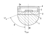
- FIG. 1 is an example of the organic light-emitting device of the present invention.
- the organic light emitting element includes a substrate 2, an organic electroluminescence element 3 formed on the surface of the substrate 2, and a lens 1 attached to the surface of the substrate 2 opposite to the side on which the organic electroluminescence element 3 is formed.
- the organic electroluminescence element 3 is sealed by the sealing portion 4.
- the organic electroluminescence element 3 As the organic electroluminescence element 3, a normal layer configuration can be used. Specifically, the light emitting layer is sandwiched between an electrode provided on the surface of the substrate 2 and a counter electrode facing the electrode. In rare cases, a layer in which a hole transport layer, a hole injection layer, an electron transport layer, an electron injection layer, a carrier block layer, an intermediate layer, or the like is laminated between the electrode and the counter electrode as necessary is used. Can do. The illustration and detailed description of these layers are omitted. As the electrode and the counter electrode, the side from which light is extracted is preferably a transparent electrode.
- the element structure and emission color of the organic electroluminescence element 3 are not particularly limited, and a general element structure or emission color such as a single layer element, a multi-unit element, a white light emitting element, or a single color light emitting element is used. Can do.
- the organic electroluminescent element 3 has a light emitting part 5 that emits light generated by an organic electric field reaction to the outside.
- the light emitting part 5 is in contact with the substrate 2 of the organic electroluminescent element 3. It is the surface. That is, in the organic electroluminescence element 3, the light emitting portion 5 is formed in a plane parallel to the substrate 2, and the light emitted in a planar shape is emitted in a direction perpendicular to the substrate 2. Yes.
- the surface shape of the electrode provided in contact with the substrate 2 and the light emitting layer are different, the surface shape portion of the light emitting layer is the light emitting portion among the portions where the substrate 2 and the organic electroluminescence element 3 are in contact with each other. 5
- the film structure (surface shape) of the organic electroluminescence element 3 and the surface shape of the light emitting portion 5 are not particularly limited, and are not particularly limited as long as good light emission efficiency can be obtained. It is preferable that the device is designed so that more light is emitted to the outside in order to obtain highly efficient characteristics.
- the light emitting unit 5 can be formed in a circular shape, a square shape, a rectangular shape, an elliptical shape, or the like. Moreover, it is also preferable to make it the shape (similar shape) with the same area as the shape of the part where the lens 1 of the board
- the attached portion of the lens 1 is circular and the light emitting portion 5 is circular, and in this case, the centers of the circles are preferably coincident.
- the radius of the light emitting unit 5 is preferably 0.1 to 50 mm.
- the radius of the light emitting portion 5 is within this range, a more efficient organic light emitting element can be obtained. If the radius of the light-emitting portion 5 is smaller than this range, high light emission may not be obtained. If the radius of the light emitting portion 5 is larger than this range, the light emission characteristics of the organic electroluminescence element 3 itself may be deteriorated.
- a transparent substrate 2 formed of a light-transmitting material such as glass or plastic can be used in order to efficiently extract light generated in the organic electroluminescence element 3.
- a glass substrate or a transparent substrate can be used.
- a resin substrate or the like can be used.
- the thickness of the substrate 2 is preferably 0.1 to 50 mm. When the thickness of the substrate 2 is within this range, a more efficient organic light emitting device can be obtained. When the thickness of the substrate 2 is thinner than this range, the strength of the organic light emitting element may be weakened. On the other hand, if the thickness of the substrate 2 is larger than this range, light may be absorbed by the substrate 2 and the light may not be extracted efficiently.
- the lens 1 is not particularly limited as long as it is a lens 1 for a light emitting element.
- a lens 1 having a circular shape parallel to the substrate 2 such as a hemispherical lens or a convex lens is used. it can.
- the material of the lens 1 is not particularly limited as long as light emitted from the organic electroluminescence element 3 can be taken out efficiently, and various light-transmitting materials such as glass and plastic can be used. .
- the diameter of the lens 1 is preferably 0.1 to 50 mm. When the diameter of the lens 1 is within this range, a more efficient organic light emitting device can be obtained. If the diameter of the lens 1 is smaller than this range, the light emitting section 5 is also small in order to satisfy the condition of the angle ⁇ described later, so that high light emission may not be obtained. If the diameter of the lens 1 is larger than this range, the light emitting portion 5 may be relatively small and high light emission may not be obtained.
- the organic light emitting element may be formed by handling the lens 1 and the substrate 2 as a lens substrate integrated with each other.
- the sealing part 4 is not particularly limited as long as the organic electroluminescence element 3 can be sealed and protected from the outside, and may be sealed using sealing glass or the like, or may be made of resin. You may seal using a sealing material.
- the sealing portion 4 having a U-shaped cross-section with the lower surface opened is provided on the surface of the substrate 2 so that the positions of the end portion of the lens 1 and the end portion of the sealing portion 4 coincide on the front and back of the substrate 2 Is provided.
- the area of the light emitting portion 5 parallel to the substrate surface is smaller than the area of the substrate 2 where the lens 1 is attached (lens attached area). That is, the area of the surface (first contact surface) that contacts the surface of the substrate 2 of the light emitting unit 5 in parallel is smaller than the area of the surface (second contact surface) of the lens 1 that contacts the substrate 2 in parallel.
- An angle ⁇ formed by a perpendicular line L ⁇ of the substrate surface 2a (or the first contact surface) in the direction from the light emitting unit 5 to the substrate 2 and a straight line L1 connecting the end of the light emitting unit 5 and the end of the lens is It is 60 degrees or more.
- both the first and second contact surfaces are formed in a circular shape and arranged so that the optical axis M1 of the light emitting unit 5 coincides with the central axis of the lens 1 as shown in FIG. Luminescence can be obtained.
- the perpendicular line L ⁇ to the first contact surface and the left end portions of the first and second contact surfaces in the cross section cut in the vertical direction along the optical axis M1 as shown in FIG. 1 of the organic light emitting device of the present invention, the perpendicular line L ⁇ to the first contact surface and the left end portions of the first and second contact surfaces.
- the angle ⁇ formed by the straight line L1 connecting each other may be 60 degrees or more.
- the size of the light emitting area when the lens attachment area is 100% is less than 100%, but is preferably 5% or more, more preferably 10 to 80%. If the size of the light emitting portion area relative to the lens attachment area becomes too small, there is a possibility that the emitted light cannot be taken out sufficiently. If the size of the light emitting area is too close to the size of the lens attachment area, the angle ⁇ may not be maintained at 60 degrees or more, and light may not be extracted efficiently.
- the angle ⁇ formed by the perpendicular line L ⁇ of the substrate surface 2a in the direction from the light emitting unit 5 to the substrate 2 and the straight line L1 connecting the end of the light emitting unit 5 and the end of the lens is 60 degrees or more and 90 degrees or less. However, it is more preferably 70 to 90 degrees. When the angle ⁇ is within this range, light can be extracted more efficiently.
- the refractive index of the lens 1 is more than the refractive index of the substrate 2, and the refractive index of the lens 1 is more preferably larger than the refractive index of the substrate 2. Accordingly, it is possible to prevent light emitted at the interface between the substrate 2 and the lens 1 from being totally reflected and cannot be extracted to the outside, and to efficiently extract light to the outside. If the refractive index of the lens 1 is lower than the refractive index of the substrate 2, the light extraction efficiency decreases.
- the refractive index of both the substrate 2 and the lens 1 is 1.7 or more.
- the emitted light is totally reflected at the interface between the electrode of the organic electroluminescence element 3 and the substrate 2 and cannot be extracted to the outside, or the light is totally reflected at the interface between the substrate 2 and the lens 1 to the outside. It is possible to prevent the light from being extracted and to extract light to the outside more efficiently.
- the substrate 2 can be set to 1.7 to 1.9
- the lens 1 can be set to 1.7 to 1.9.
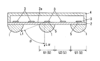
- FIG. 2 shows another example of the organic light-emitting device of the present invention.
- a plurality of lenses 1 are attached to the surface of the substrate 2 at equal intervals to form a lens array substrate 10, and each surface of the substrate 2 opposite to the surface on which the lens 1 is attached is arranged on each surface.
- a plurality of organic electroluminescence elements 3 are provided at equal intervals in an arrangement corresponding to the lens 1. That is, the number of the organic electroluminescence elements 3 and the lenses 1 is the same, and their centers (centers in a plane parallel to the substrate 2) are arranged to coincide.
- one lens 1 and another lens 1 adjacent to the lens 1 are provided in contact with each other.
- the sealing part 4 may seal all the plurality of organic electroluminescence elements 3 together with one sealing part 4 as shown in the figure, or each organic electroluminescence element 3 may be individually sealed. You may do.
- each light emitting unit U has the same configuration as that of the embodiment of FIG. It has become. That is, in each light emitting unit U, the area of the light emitting part is smaller than the area provided with the lens, the perpendicular line L ⁇ of the substrate surface 2a in the direction from the light emitting part 5 toward the substrate 2, the end of the light emitting part 5 and the end of the lens.
- the angle ⁇ formed by the straight line L1 connecting the portions is 60 degrees or more, whereby the light of each light emitting unit can be efficiently extracted.
- the light emitting unit U is a pixel of the light emitting element.
- FIG. 3 shows another example of the organic light emitting device of the present invention.
- a plurality of organic electroluminescence elements 3 are provided on the surface of the substrate 2 at equal intervals, and a plurality of organic electroluminescence elements 3 are provided on the surface of the substrate 2 opposite to the surface on which the organic electroluminescence elements 3 are provided.
- the lens 1 is provided in an arrangement corresponding to a part of the plurality of organic electroluminescence elements 3. That is, the number of lenses 1 is smaller than that of the organic electroluminescence elements 3, and each lens 1 is arranged so that the center (center in a plane parallel to the substrate 2) coincides with the individual organic electroluminescence elements 3. Yes.
- the lenses 1 may be attached at regular intervals, that is, corresponding to every other predetermined number of the organic electroluminescence elements 3, or may be attached at a desired arrangement instead of at regular intervals.
- the sealing part 4 can be configured similarly to the form of FIG.
- the lens 1 is provided on the surface of the substrate 2 opposite to the organic electroluminescence element 3 among the light emitting units U composed of the organic electroluminescence element 3 and a part of the substrate 2 on which the organic electroluminescence element 3 is provided.
- each light emitting unit U1 has the same configuration as that of the embodiment of FIG. That is, in each light emitting unit U1, the area of the light emitting portion is smaller than the area provided with the lens, the perpendicular line L ⁇ of the substrate surface 2a in the direction from the light emitting portion 5 to the substrate 2, the end of the light emitting portion 5 and the end of the lens.
- the angle ⁇ formed by the straight line L1 connecting the portions is 60 degrees or more, whereby the light of each light emitting unit U1 can be efficiently extracted.
- the light emitting unit U2 in which the lens 1 is not provided among the light emitting units U the light that has passed through the substrate 2 is emitted as it is to the outside.
- the lens 1 can be arranged only in the light emitting unit U that requires high light extraction efficiency to extract light, and an organic light emitting element that can emit light efficiently can be obtained. It is.
- FIG. 4 shows another example of the organic light-emitting device of the present invention.
- a plurality of organic electroluminescent elements 3 having different sizes (light emitting portion areas) are provided on the surface of the substrate 2 and opposite to the surface of the substrate 2 on which the organic electroluminescent elements 3 are provided.
- a plurality of lenses 1 having different sizes (lens-attached areas) are provided on the side surface in an arrangement corresponding to each of the organic electroluminescence elements 3.
- the organic electroluminescence element 3 and the lens 1 are arranged at equal intervals so that their centers (centers in a plane parallel to the substrate 2) coincide with each other, and are large for the large organic electroluminescence element 3.
- a lens 1 is assigned, and a small lens 1 is assigned to a small organic electroluminescence element 3.
- each light emitting unit U includes a light emitting unit 5 having a large area or a small area.
- the configuration is the same as that of the embodiment of FIG. That is, in each light emitting unit U, the area of the light emitting part is smaller than the area provided with the lens, the perpendicular line L ⁇ of the substrate surface 2a in the direction from the light emitting part 5 toward the substrate 2, the end of the light emitting part 5 and the end of the lens.
- the angle ⁇ formed by the straight line L1 connecting the portions is 60 degrees or more, whereby the light of each light emitting unit U can be efficiently extracted.
- the angle ⁇ ( ⁇ 1) in the light emission unit U of the large lens 1 and the angle ⁇ ( ⁇ 2) in the light emission unit U ′ of the small lens 1 may be the same or different.
- the area of the light emitting portion 5 and the size of the lens 1 can be adjusted to combine the light emitting units U of various sizes, and the device can be configured to emit light efficiently. An organic light emitting device can be obtained.
- FIG. 5 shows another example of the organic light-emitting device of the present invention.
- the organic electroluminescent element 3 is a double-sided light emitting organic electroluminescent element 3 capable of emitting light in both the direction toward the substrate 2 and the direction opposite to the substrate 2. That is, the light emitting unit 5 is formed on both surfaces of the light emitting unit 5a on the surface disposed on the substrate side and the light emitting unit 5b on the surface opposite to the substrate.
- substrate 2, the lens 1, and the organic electroluminescent element 3 becomes the structure similar to the form of FIG.
- a plurality of lenses 1 are attached to the surface of the substrate 2 at equal intervals to form the lens array substrate 10, and the surface of the substrate 2 opposite to the surface on which the lens 1 is attached is
- a plurality of organic electroluminescence elements 3 are provided at equal intervals in an arrangement corresponding to each lens 1, and the centers of the organic electroluminescence elements 3 and the lenses 1 coincide with each other.
- the sealing part 4 encloses the circumference
- the lens structure portion 6 is provided on the surface opposite to the substrate 2.
- the sealing resin portion 11 is formed by a liquid sealing resin covering and curing the organic electroluminescence element 3, and the surface opposite to the substrate 2 is formed to be substantially flat.
- the lens structure portion 6 is composed of a plurality of lens bodies 12, and each lens body 12 is attached to the surface of the sealing resin portion 11 at equal intervals with the center position aligned with the center of each organic electroluminescence element 3.
- the lens body 12 is arranged so that the center thereof also coincides with the center of the lens 1.
- the lens body 12 can be a glass lens, a resin lens, or the like, and can be made of the same material as the lens 1.
- the size of each lens body 12 may be formed substantially the same as that of the lens 1 or may be different from that of the lens 1.
- the light emitting unit U is composed of the organic electroluminescence element 3, the lens 1, the lens body 12, the substrate 2 sandwiched between the lens 1 and the lens body 12, and a part of the sealing resin portion 11. ing.
- the structure on the side where the lens 1 of the substrate 2 is provided has the same configuration as that of the embodiment of FIG. That is, in each light emitting unit U, the light emitting portion area of the light emitting portion 5a is smaller than the lens mounting area of the lens 1, and the perpendicular line L ⁇ of the substrate surface 2a in the direction from the light emitting portion 5a toward the substrate 2 and the light emitting portion 5a.
- the angle ⁇ formed by the straight line L1 connecting the end of the lens and the end of the lens is 60 degrees or more, so that the light of each light emitting unit U can be efficiently extracted to the substrate side. Yes.
- the structure similar to the above is also formed on the lens body 12 side of the organic electroluminescence element 3. That is, in each light emitting unit U, the light emitting portion area of the light emitting portion 5b (the area of the surface parallel to the substrate surface of the light emitting portion 5b) is the lens attachment area of the lens body 12 (the lens body 12 of the sealing resin portion 11 is attached).
- the straight line L2 perpendicular to the substrate surface 2a in the direction from the light emitting part 5b toward the lens body 12, and the straight line L2 connecting the end of the light emitting part 5b and the end of the lens body 12 And the angle ⁇ is 60 degrees or more.
- Example 1 First, a glass substrate with ITO in which 1100 mm thick ITO (Indium Tin Oxide, sheet resistance 12 ⁇ / ⁇ ) was formed on one surface of a 0.5 mm thick glass substrate (refractive index 1.51) was prepared. This glass substrate with ITO was subjected to ultrasonic cleaning with pure water, acetone and isopropyl alcohol for 10 minutes each, then steam cleaned with isopropyl alcohol vapor for 2 minutes, dried, and further UV ozone cleaned for 10 minutes.
- ITO Indium Tin Oxide, sheet resistance 12 ⁇ / ⁇
- the ITO-attached glass substrate was set in a vacuum deposition apparatus, and a 1: 1 co-deposition film of molybdenum oxide (MoO 3 ) and ⁇ -NPD was used as a hole injection layer under a reduced pressure of 5 ⁇ 10 ⁇ 5 Pa. Vapor deposited thick.
- ⁇ -NPD was vapor-deposited as a hole transport layer in a thickness of 300 mm, and then a green phosphorescent light-emitting layer doped with 10% Ir (ppy) 3 in CBP was vapor-deposited as a light-emitting layer in a thickness of 300 mm. It was further deposited Alq 3 to 500 ⁇ thick as an electron transport layer.
- LiF was vapor-deposited to a thickness of 5 mm
- Al was vapor-deposited to a thickness of 1000 mm to produce an organic electroluminescence element.
- the shape of the light emitting part was a circle having a radius of 1.5 mm, and the area was about 7.07 mm 2 .
- a hemispherical lens (refractive index of 1.51) having a diameter of 5 mm was adhered to the surface of the glass substrate opposite to the surface on which the organic electroluminescence element was produced using a liquid adhesive having a refractive index of 1.51.
- the area where the hemispherical lens was attached was about 19.6 mm 2 .
- Example 2 The shape of the light emitting part was a circle having a radius of 0.5 mm (area of about 0.785 mm 2 ). Other than that produced the organic light emitting element similarly to Example 1.
- FIG. That is, an organic electroluminescence element having the same layer structure is formed on the surface of the glass substrate, and a hemispherical lens having a diameter of 5 mm (refractive index 1.51) is adhered to the glass substrate using a liquid adhesive having a refractive index of 1.51. Then, adjustment was made so that the hemispherical lens and the center of the circle of the light emitting portion coincided, and an organic light emitting device was fabricated.
- Example 3 A glass substrate with ITO in which 1100 mm thick ITO (sheet resistance 12 ⁇ / ⁇ ) was formed on one side of a 0.5 mm thick glass substrate (refractive index 1.75) was prepared. Next, an organic electroluminescence element having the same layer structure as in Example 1 was produced (light emitting portion: a circle having a radius of 1.5 mm, an area of about 7.07 mm 2 ).
- a hemispherical lens (refractive index: 1.75) having a diameter of 5 mm was brought into close contact with the surface of the glass substrate opposite to the surface on which the organic electroluminescence element was produced, using a liquid adhesive having a refractive index of 1.75.
- the area where the hemispherical lens was attached was about 19.6 mm 2 .
- Example 4 A glass substrate with ITO in which 1100 mm thick ITO (sheet resistance 12 ⁇ / ⁇ ) was formed on one surface of a 0.5 mm thick glass substrate (refractive index 1.90) was prepared. Next, an organic electroluminescence element having the same layer structure as in Example 1 was produced (light emitting portion: a circle having a radius of 1.5 mm, an area of about 7.07 mm 2 ).
- a hemispherical lens (refractive index: 1.90) having a diameter of 5 mm was brought into close contact with the surface of the glass substrate opposite to the surface on which the organic electroluminescence element was produced, using a liquid adhesive having a refractive index of 1.90.
- the area where the hemispherical lens was attached was about 19.6 mm 2 .
- Example 5 A glass substrate with ITO in which 1100 mm thick ITO (sheet resistance 12 ⁇ / ⁇ ) was formed on one side of a 0.5 mm thick glass substrate (refractive index 1.51) was prepared. Next, an organic electroluminescence element having the same layer structure as in Example 1 was produced (light emitting portion: a circle having a radius of 1.5 mm, an area of about 7.07 mm 2 ).
- a hemispherical lens (refractive index: 1.75) having a diameter of 5 mm was brought into close contact with the surface of the glass substrate opposite to the surface on which the organic electroluminescence element was produced, using a liquid adhesive having a refractive index of 1.75.
- the area where the hemispherical lens was attached was about 19.6 mm 2 .
- Example 6 A glass substrate with ITO in which 1100 mm thick ITO (sheet resistance 12 ⁇ / ⁇ ) was formed on one side of a 0.5 mm thick glass substrate (refractive index 1.51) was prepared. Next, an organic electroluminescence element having the same layer structure as in Example 1 was produced (light emitting portion: a circle having a radius of 1.5 mm, an area of about 7.07 mm 2 ).
- a hemispherical lens (refractive index: 1.90) having a diameter of 5 mm was brought into close contact with the surface of the glass substrate opposite to the surface on which the organic electroluminescence element was produced, using a liquid adhesive having a refractive index of 1.90.
- the area where the hemispherical lens was attached was about 19.6 mm 2 .
- Example 7 A glass substrate with ITO in which 1100 mm thick ITO (sheet resistance 12 ⁇ / ⁇ ) was formed on one side of a 0.5 mm thick glass substrate (refractive index 1.51) was prepared. And the light emitting layer was formed into a film by the method similar to Example 1.
- a hemispherical lens (refractive index of 1.51) having a diameter of 5 mm was adhered to the surface of the glass substrate opposite to the surface on which the organic electroluminescence element was produced using a liquid adhesive having a refractive index of 1.51.
- the area where the hemispherical lens was attached was about 19.6 mm 2 .
- a glass substrate having a lens structure on its surface was bonded to the surface of the glass substrate on which the organic electroluminescence element was produced using a UV curable resin having a refractive index of 1.51 to form a sealing portion having a lens structure portion.
- the lens shape was a hemispherical lens in which the attached portion was a circle with a diameter of 5 mm. At the time of bonding, adjustment was made so that the center of the circle of the lens structure coincided with the center of the circle of the light emitting portion. Thus, a double-sided organic light emitting device was produced.
- Example 1 The shape of the light emitting portion and the circular radius 2 mm (area of about 12.56mm 2). Other than that produced the organic light emitting element similarly to Example 1.
- the shape of the light emitting part was a circle having a radius of 2.5 mm (diameter 5 mm) (area of about 19.6 mm 2 ). Other than that produced the organic light emitting element similarly to Example 1.
- FIG. That is, an organic electroluminescence element having the same layer structure is formed on the surface of the glass substrate, and a hemispherical lens having a diameter of 5 mm (refractive index 1.51) is adhered to the glass substrate using a liquid adhesive having a refractive index of 1.51. Then, adjustment was made so that the hemispherical lens and the circle center of the light emitting portion coincided with each other, and an organic light emitting device was produced.
- Example 3 A glass substrate with ITO in which 1100 mm thick ITO (sheet resistance 12 ⁇ / ⁇ ) was formed on one surface of a 0.5 mm thick glass substrate (refractive index 1.90) was prepared. Next, an organic electroluminescence element having the same layer structure as in Example 1 was produced (light emitting portion: a circle having a radius of 1.5 mm, an area of about 7.07 mm 2 ).
- a hemispherical lens (refractive index of 1.51) having a diameter of 5 mm was adhered to the surface of the glass substrate opposite to the surface on which the organic electroluminescence element was produced using a liquid adhesive having a refractive index of 1.51.
- the area where the hemispherical lens was attached was about 19.6 mm 2 .
- Example 4 A glass substrate with ITO in which 1100 mm thick ITO (sheet resistance 12 ⁇ / ⁇ ) was formed on one surface of a 0.5 mm thick glass substrate (refractive index 1.90) was prepared. Next, an organic electroluminescence element having the same layer structure as in Example 1 was produced (light emitting portion: a circle having a radius of 1.5 mm, an area of about 7.07 mm 2 ).
- a hemispherical lens (refractive index: 1.75) having a diameter of 5 mm was brought into close contact with the surface of the glass substrate opposite to the surface on which the organic electroluminescence element was produced, using a liquid adhesive having a refractive index of 1.75.
- the area where the hemispherical lens was attached was about 19.6 mm 2 .
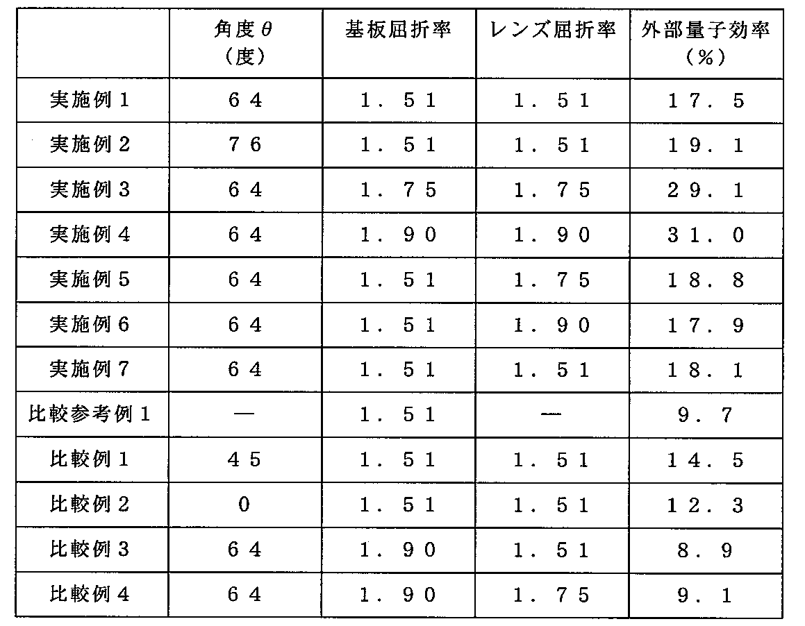
- Table 1 shows, along with the external quantum efficiency, an angle ⁇ (an angle formed by a perpendicular line L ⁇ of the substrate surface 2a in the direction from the light emitting portion toward the substrate and a straight line L1 connecting the end portion of the light emitting portion and the end portion of the lens), the substrate The refractive index of the lens and the refractive index of the lens are listed.
- External quantum efficiency is a result of the angle-resolved measurement at a current density of 2 mA / cm 2.
- Example 1 was able to obtain a highly efficient organic light-emitting device as compared with Comparative Examples 1 and 2 by setting the angle ⁇ to 64 degrees.
- Example 2 a more efficient organic light-emitting device could be obtained by setting the angle ⁇ to 76 degrees.
- the angle ⁇ was set to 64 degrees, and both the refractive index of the lens and the substrate were set to 1.7 or more, whereby a highly efficient organic light-emitting device could be obtained.
- Example 4 the angle ⁇ was set to 64 degrees, and the refractive index of both the lens and the substrate was set to 1.9, whereby a highly efficient organic light emitting device could be obtained.
- Example 5 it was possible to obtain a highly efficient organic light emitting device by setting the angle ⁇ to 64 degrees and making the refractive index of the lens larger than the refractive index of the substrate.
- Example 7 the angle ⁇ and the angle ⁇ were 64 degrees, and a lens shape was provided on both sides of the light emitting surface of the double-sided light emitting device, whereby a highly efficient organic light emitting device could be obtained.
Landscapes
- Physics & Mathematics (AREA)
- Optics & Photonics (AREA)
- Electroluminescent Light Sources (AREA)
Abstract
Description
より高効率な有機発光素子を得ることができ、更には素子の作製が容易となる。
まず、厚み0.5mmのガラス基板(屈折率1.51)の片面に1100Å厚のITO(Indium Tin Oxide、シート抵抗12Ω/□)が形成されたITO付きガラス基板を用意した。このITO付きガラス基板を純水、アセトン、イソプロピルアルコールで各10分間超音波洗浄した後、イソプロピルアルコール蒸気で2分間蒸気洗浄して、乾燥し、さらに10分間UVオゾン洗浄した。
発光部の形状を半径0.5mmの円形にした(面積約0.785mm2)。それ以外は、実施例1と同様に有機発光素子を作製した。すなわち、ガラス基板の表面に同様の層構成で有機エレクトロルミネッセンス素子を形成し、直径5mmの半球レンズ(屈折率1.51)を屈折率1.51の液体接着剤を用いてガラス基板に密着させ、半球レンズと発光部の円中心とが一致するように調整し、有機発光素子を作製した。
厚み0.5mmのガラス基板(屈折率1.75)の片面に1100Å厚のITO(シート抵抗12Ω/□)が形成されたITO付きガラス基板を用意した。次に、実施例1と同様の層構成の有機エレクトロルミネッセンス素子を作製した(発光部:半径1.5mmの円形、面積約7.07mm2)。
厚み0.5mmのガラス基板(屈折率1.90)の片面に1100Å厚のITO(シート抵抗12Ω/□)が形成されたITO付きガラス基板を用意した。次に、実施例1と同様の層構成の有機エレクトロルミネッセンス素子を作製した(発光部:半径1.5mmの円形、面積約7.07mm2)。
厚み0.5mmのガラス基板(屈折率1.51)の片面に1100Å厚のITO(シート抵抗12Ω/□)が形成されたITO付きガラス基板を用意した。次に、実施例1と同様の層構成の有機エレクトロルミネッセンス素子を作製した(発光部:半径1.5mmの円形、面積約7.07mm2)。
厚み0.5mmのガラス基板(屈折率1.51)の片面に1100Å厚のITO(シート抵抗12Ω/□)が形成されたITO付きガラス基板を用意した。次に、実施例1と同様の層構成の有機エレクトロルミネッセンス素子を作製した(発光部:半径1.5mmの円形、面積約7.07mm2)。
厚み0.5mmのガラス基板(屈折率1.51)の片面に1100Å厚のITO(シート抵抗12Ω/□)が形成されたITO付きガラス基板を用意した。そして、実施例1と同様の方法で発光層までを成膜した。次に、発光層の上に、電子輸送層としてAlq3を300Å厚に蒸着した。その上にAlq3とLiの共蒸着層を200Å成膜した。その上に陰極としてIZOをスパッタ法を用いて成膜することにより、両面発光素子となった有機エレクトロルミネッセンス素子を作製した。
実施例1と同様に、有機エレクトロルミネッセンス素子を作製し、半球レンズを貼り付けることなく特性の評価を行った。
発光部の形状を半径2mmの円形にした(面積約12.56mm2)。それ以外は、実施例1と同様に有機発光素子を作製した。すなわち、ガラス基板の表面に同様の層構成で有機エレクトロルミネッセンス素子を形成し、直径5mmの半球レンズ(屈折率1.51)を屈折率1.51の液体接着剤を用いてガラス基板に密着させ、半球レンズと発光部の円中心とが一致するように調整し、有機発光素子を作製した。
発光部の形状を半径2.5mm(直径5mm)の円形にした(面積約19.6mm2)。それ以外は、実施例1と同様に有機発光素子を作製した。すなわち、ガラス基板の表面に同様の層構成で有機エレクトロルミネッセンス素子を形成し、直径5mmの半球レンズ(屈折率1.51)を屈折率1.51の液体接着剤を用いてガラス基板に密着させ、半球レンズと発光部の円中心とが一致するように調整し、有機発光素子を作製した。
厚み0.5mmのガラス基板(屈折率1.90)の片面に1100Å厚のITO(シート抵抗12Ω/□)が形成されたITO付きガラス基板を用意した。次に、実施例1と同様の層構成の有機エレクトロルミネッセンス素子を作製した(発光部:半径1.5mmの円形、面積約7.07mm2)。
厚み0.5mmのガラス基板(屈折率1.90)の片面に1100Å厚のITO(シート抵抗12Ω/□)が形成されたITO付きガラス基板を用意した。次に、実施例1と同様の層構成の有機エレクトロルミネッセンス素子を作製した(発光部:半径1.5mmの円形、面積約7.07mm2)。
表1に、外部量子効率とともに、角度θ(発光部から基板に向かう方向の基板面2aの垂線Lαと、発光部の端部とレンズの端部とを結ぶ直線L1とのなす角度)、基板の屈折率、レンズの屈折率を列挙した。外部量子効率は電流密度2mA/cm2での角度分解測定の結果である。
Claims (8)
- 基板と、
前記基板の一方の表面に形成され、前記基板に向かって発光する発光部を有する有機エレクトロルミネッセンス素子と、
前記基板の他方の表面に付設され、前記基板の屈折率以上の屈折率を有するレンズと、を備え、
前記発光部の前記基板表面と平行な面の面積は、前記基板の前記レンズを付設している面積よりも小さく、
前記発光部から前記基板に向かう方向の基板面の垂線と、前記発光部の端部と前記レンズの端部とを結ぶ直線とのなす角度が60度以上であることを特徴とする有機発光素子。 - 前記有機エレクトロルミネッセンス素子が、前記基板に向かう方向と前記基板と反対側の方向との両方向に発光可能なものであると共に、前記有機エレクトロルミネッセンス素子の前記基板とは反対側にレンズ構造部が設けられたことを特徴とする請求項1に記載の有機発光素子。
- 前記レンズの屈折率が前記基板の屈折率よりも大きいことを特徴とする請求項1又は2に記載の有機発光素子。
- 前記基板と前記レンズの屈折率がともに1.7以上であることを特徴とする請求項1から3のいずれか1項に記載の有機発光素子。
- 前記発光部は、積層構造を有して、前記基板表面と平行に接触する第1の接触面を備え、
前記レンズは、前記基板と平行に接触する第2の接触面を備え、
前記第1の接触面の面積は、前記第2の接触面の面積よりも小さく設定されることを特徴とする請求項1から4のいずれか1項に記載の有機発光素子。 - 前記第1及び第2の接触面は、互いに相似形状に形成されることを特徴とする請求項5に記載の有機発光素子。
- 少なくとも前記第1の接触面の一部を通るように垂直方向に切った断面において、前記第1の接触面に対する垂線と、前記第1及び第2の接触面の左端部同士又は右端部同士を結ぶ直線と、が成す角度が60度以上であることを特徴とする請求項5又は6に記載の有機発光素子。
- 前記第1及び第2の接触面は、それぞれ円形状に形成され、
前記発光部は、光軸が前記レンズの中心軸と一致するように配置され、
前記光軸に沿って垂直方向に切った断面において、前記第1の接触面に対する垂線と、前記第1及び第2の接触面の左端部同士又は右端部同士を結ぶ直線と、が成す角度が60度以上であることを特徴とする請求項5に記載の有機発光素子。
Priority Applications (4)
| Application Number | Priority Date | Filing Date | Title |
|---|---|---|---|
| US13/392,748 US8519610B2 (en) | 2009-09-01 | 2010-09-01 | Organic luminescent element |
| EP10813703.5A EP2475222A4 (en) | 2009-09-01 | 2010-09-01 | ORGANIC LUMINESCENT ELEMENT |
| CN201080037829.9A CN102612857B (zh) | 2009-09-01 | 2010-09-01 | 有机发光元件 |
| KR1020127006187A KR101335369B1 (ko) | 2009-09-01 | 2010-09-01 | 유기 발광 소자 |
Applications Claiming Priority (2)
| Application Number | Priority Date | Filing Date | Title |
|---|---|---|---|
| JP2009201956A JP5480567B2 (ja) | 2009-09-01 | 2009-09-01 | 有機発光素子 |
| JP2009-201956 | 2009-09-01 |
Publications (1)
| Publication Number | Publication Date |
|---|---|
| WO2011027754A1 true WO2011027754A1 (ja) | 2011-03-10 |
Family
ID=43649289
Family Applications (1)
| Application Number | Title | Priority Date | Filing Date |
|---|---|---|---|
| PCT/JP2010/064868 WO2011027754A1 (ja) | 2009-09-01 | 2010-09-01 | 有機発光素子 |
Country Status (6)
| Country | Link |
|---|---|
| US (1) | US8519610B2 (ja) |
| EP (1) | EP2475222A4 (ja) |
| JP (1) | JP5480567B2 (ja) |
| KR (1) | KR101335369B1 (ja) |
| CN (1) | CN102612857B (ja) |
| WO (1) | WO2011027754A1 (ja) |
Cited By (1)
| Publication number | Priority date | Publication date | Assignee | Title |
|---|---|---|---|---|
| CN103364912A (zh) * | 2012-04-11 | 2013-10-23 | 全球微型光学有限公司 | 光学透镜组 |
Families Citing this family (11)
| Publication number | Priority date | Publication date | Assignee | Title |
|---|---|---|---|---|
| JP2012038632A (ja) * | 2010-08-10 | 2012-02-23 | Canon Inc | 有機エレクトロルミネッセンス表示装置 |
| JP5637027B2 (ja) * | 2011-03-22 | 2014-12-10 | 日本ゼオン株式会社 | レンズアレイシート及び発光装置 |
| TW201250999A (en) * | 2011-06-13 | 2012-12-16 | Wintek Corp | Organic electroluminescent display device |
| JP5803506B2 (ja) * | 2011-09-28 | 2015-11-04 | 日本ゼオン株式会社 | 発光素子及び照明器具 |
| JP2013200964A (ja) * | 2012-03-23 | 2013-10-03 | Harison Toshiba Lighting Corp | 発光装置 |
| KR101894342B1 (ko) | 2013-12-27 | 2018-09-03 | 제이엑스티지 에네루기 가부시키가이샤 | 발광 소자 |
| JP6599315B2 (ja) | 2014-04-28 | 2019-10-30 | Jxtgエネルギー株式会社 | 発光素子 |
| DE102015007830B4 (de) * | 2015-06-18 | 2017-12-28 | e.solutions GmbH | Optische Baugruppe, elektronisches Gerät und Kraftfahrzeug mit einer optischen Baugruppe sowie Verfahren zum Herstellen einer optischen Baugruppe |
| WO2017158775A1 (ja) * | 2016-03-16 | 2017-09-21 | パイオニア株式会社 | 発光装置及び発光システム |
| KR102482762B1 (ko) * | 2017-01-10 | 2022-12-29 | 서울바이오시스 주식회사 | 포충기 |
| DE102017004562A1 (de) * | 2017-05-14 | 2018-11-15 | Docter Optics Se | Verfahren zum Herstellen eines Mikroprojektors und eines Projektionsdisplays |
Citations (8)
| Publication number | Priority date | Publication date | Assignee | Title |
|---|---|---|---|---|
| JPH10208875A (ja) | 1997-01-27 | 1998-08-07 | Hokuriku Electric Ind Co Ltd | 有機el素子とその製造方法 |
| JP2003059642A (ja) * | 2001-08-09 | 2003-02-28 | Matsushita Electric Ind Co Ltd | 有機エレクトロルミネッセンス素子、それを用いた照明装置、表示装置及び携帯端末 |
| JP2004039500A (ja) | 2002-07-04 | 2004-02-05 | Seiko Epson Corp | 有機エレクトロルミネッセンス装置、有機エレクトロルミネッセンス装置の製造方法及び電子機器 |
| JP2004227940A (ja) * | 2003-01-23 | 2004-08-12 | Seiko Epson Corp | 表示体、表示パネル、表示装置および製造方法 |
| JP2005310749A (ja) * | 2004-04-19 | 2005-11-04 | Samsung Sdi Co Ltd | 平板表示装置 |
| WO2006022273A2 (ja) * | 2004-08-24 | 2006-03-02 | Tohoku Device Co Ltd | 有機el素子と、有機el素子の保護膜及びその製法 |
| JP2006116706A (ja) * | 2004-10-19 | 2006-05-11 | Seiko Epson Corp | 透明基板、電気光学装置、画像形成装置及び電気光学装置の製造方法 |
| JP2006150707A (ja) * | 2004-11-29 | 2006-06-15 | Seiko Epson Corp | 透明基板、電気光学装置、画像形成装置及び電気光学装置の製造方法 |
Family Cites Families (13)
| Publication number | Priority date | Publication date | Assignee | Title |
|---|---|---|---|---|
| JPH10223367A (ja) * | 1997-02-04 | 1998-08-21 | Mitsubishi Chem Corp | 有機電界発光素子 |
| JP2000322000A (ja) * | 1999-05-10 | 2000-11-24 | Canon Inc | 表示装置 |
| WO2001033598A1 (en) * | 1999-10-29 | 2001-05-10 | Trustees Of Princeton University | Organic light emitting diode having spherical shaped patterns |
| JP2002049326A (ja) * | 2000-08-02 | 2002-02-15 | Fuji Photo Film Co Ltd | 平面光源およびそれを用いた表示素子 |
| JP2003260812A (ja) * | 2002-03-11 | 2003-09-16 | Seiko Epson Corp | 光印写ヘッド及びそれを用いた画像形成装置 |
| JP2004241130A (ja) * | 2003-02-03 | 2004-08-26 | Seiko Epson Corp | 発光ディスプレイパネルおよびその製造方法 |
| JP2005175417A (ja) * | 2003-07-28 | 2005-06-30 | Ricoh Co Ltd | 発光素子アレイ、光書込ユニットおよび画像形成装置 |
| KR100754178B1 (ko) * | 2005-08-16 | 2007-09-03 | 삼성전자주식회사 | 유기발광다이오드 어레이를 발광원으로 채용한 노광장치 및 이를 적용한 화상형성장치 |
| JP2007280699A (ja) * | 2006-04-05 | 2007-10-25 | Matsushita Electric Ind Co Ltd | 発光デバイス |
| CN101128076B (zh) * | 2007-09-14 | 2010-06-30 | 中微光电子(潍坊)有限公司 | 一种led光源的制造方法 |
| CN100489386C (zh) * | 2007-09-20 | 2009-05-20 | 胡家培 | 无反射高出光率单元wled功率扩容式大功率wled光源 |
| JP4737461B2 (ja) | 2008-07-09 | 2011-08-03 | セイコーエプソン株式会社 | 有機el露光ヘッドの製造方法 |
| JP2010135212A (ja) | 2008-12-05 | 2010-06-17 | Panasonic Corp | 発光素子、それを用いた表示装置および照明装置、ならびに発光素子の製造方法 |
-
2009
- 2009-09-01 JP JP2009201956A patent/JP5480567B2/ja not_active Expired - Fee Related
-
2010
- 2010-09-01 EP EP10813703.5A patent/EP2475222A4/en not_active Withdrawn
- 2010-09-01 WO PCT/JP2010/064868 patent/WO2011027754A1/ja active Application Filing
- 2010-09-01 US US13/392,748 patent/US8519610B2/en not_active Expired - Fee Related
- 2010-09-01 KR KR1020127006187A patent/KR101335369B1/ko not_active IP Right Cessation
- 2010-09-01 CN CN201080037829.9A patent/CN102612857B/zh not_active Expired - Fee Related
Patent Citations (8)
| Publication number | Priority date | Publication date | Assignee | Title |
|---|---|---|---|---|
| JPH10208875A (ja) | 1997-01-27 | 1998-08-07 | Hokuriku Electric Ind Co Ltd | 有機el素子とその製造方法 |
| JP2003059642A (ja) * | 2001-08-09 | 2003-02-28 | Matsushita Electric Ind Co Ltd | 有機エレクトロルミネッセンス素子、それを用いた照明装置、表示装置及び携帯端末 |
| JP2004039500A (ja) | 2002-07-04 | 2004-02-05 | Seiko Epson Corp | 有機エレクトロルミネッセンス装置、有機エレクトロルミネッセンス装置の製造方法及び電子機器 |
| JP2004227940A (ja) * | 2003-01-23 | 2004-08-12 | Seiko Epson Corp | 表示体、表示パネル、表示装置および製造方法 |
| JP2005310749A (ja) * | 2004-04-19 | 2005-11-04 | Samsung Sdi Co Ltd | 平板表示装置 |
| WO2006022273A2 (ja) * | 2004-08-24 | 2006-03-02 | Tohoku Device Co Ltd | 有機el素子と、有機el素子の保護膜及びその製法 |
| JP2006116706A (ja) * | 2004-10-19 | 2006-05-11 | Seiko Epson Corp | 透明基板、電気光学装置、画像形成装置及び電気光学装置の製造方法 |
| JP2006150707A (ja) * | 2004-11-29 | 2006-06-15 | Seiko Epson Corp | 透明基板、電気光学装置、画像形成装置及び電気光学装置の製造方法 |
Non-Patent Citations (1)
| Title |
|---|
| See also references of EP2475222A4 |
Cited By (1)
| Publication number | Priority date | Publication date | Assignee | Title |
|---|---|---|---|---|
| CN103364912A (zh) * | 2012-04-11 | 2013-10-23 | 全球微型光学有限公司 | 光学透镜组 |
Also Published As
| Publication number | Publication date |
|---|---|
| CN102612857A (zh) | 2012-07-25 |
| JP5480567B2 (ja) | 2014-04-23 |
| JP2011054407A (ja) | 2011-03-17 |
| CN102612857B (zh) | 2015-01-07 |
| EP2475222A1 (en) | 2012-07-11 |
| US20120262053A1 (en) | 2012-10-18 |
| US8519610B2 (en) | 2013-08-27 |
| KR20120090966A (ko) | 2012-08-17 |
| KR101335369B1 (ko) | 2013-12-02 |
| EP2475222A4 (en) | 2016-06-01 |
Similar Documents
| Publication | Publication Date | Title |
|---|---|---|
| JP5480567B2 (ja) | 有機発光素子 | |
| KR101471501B1 (ko) | 면상 발광 장치 | |
| JP5706916B2 (ja) | 面状発光装置 | |
| KR101135541B1 (ko) | 유기 발광 장치 | |
| US20050253788A1 (en) | Electroluminescent panel which is equipped with light xxtraction elements | |
| CN1933689A (zh) | 面发光装置 | |
| WO2013051633A1 (ja) | 発光装置 | |
| US20130056778A1 (en) | Light emitting device and method for manufacturing the same | |
| JP5334888B2 (ja) | 発光装置 | |
| US9324969B2 (en) | Lighting apparatus and lighting unit | |
| JP2010055926A (ja) | 有機エレクトロルミネッセンス素子およびその製造方法 | |
| KR20140052842A (ko) | 발광 소자 및 그것을 구비하는 표시 장치 | |
| WO2013042784A1 (ja) | 発光装置 | |
| WO2015125308A1 (ja) | 有機電界発光素子、照明装置、および照明システム | |
| JP2011216353A (ja) | 発光装置 | |
| TW201517346A (zh) | 有機發光裝置 | |
| US10162085B2 (en) | Large area organic light emitting panel | |
| JP5249606B2 (ja) | 有機el装置 | |
| JP5805618B2 (ja) | 有機発光素子およびこれを用いた照明装置 | |
| KR101924083B1 (ko) | 발광장치 및 그 제조방법 | |
| JP6630530B2 (ja) | 面発光パネル付き構造部材 | |
| KR102354235B1 (ko) | 유기발광소자 | |
| JP6380378B2 (ja) | 有機エレクトロルミネッセンス発光装置 | |
| JP2016177968A (ja) | 有機エレクトロルミネッセンスパネル及び照明装置 | |
| JP2016162555A (ja) | 有機エレクトロルミネッセンスパネル |
Legal Events
| Date | Code | Title | Description |
|---|---|---|---|
| WWE | Wipo information: entry into national phase |
Ref document number: 201080037829.9 Country of ref document: CN |
|
| 121 | Ep: the epo has been informed by wipo that ep was designated in this application |
Ref document number: 10813703 Country of ref document: EP Kind code of ref document: A1 |
|
| REEP | Request for entry into the european phase |
Ref document number: 2010813703 Country of ref document: EP |
|
| WWE | Wipo information: entry into national phase |
Ref document number: 2010813703 Country of ref document: EP |
|
| NENP | Non-entry into the national phase |
Ref country code: DE |
|
| ENP | Entry into the national phase |
Ref document number: 20127006187 Country of ref document: KR Kind code of ref document: A |
|
| WWE | Wipo information: entry into national phase |
Ref document number: 13392748 Country of ref document: US |