WO2011024296A1 - 蛍光体の製造方法およびそれにより製造された蛍光体 - Google Patents
蛍光体の製造方法およびそれにより製造された蛍光体 Download PDFInfo
- Publication number
- WO2011024296A1 WO2011024296A1 PCT/JP2009/065104 JP2009065104W WO2011024296A1 WO 2011024296 A1 WO2011024296 A1 WO 2011024296A1 JP 2009065104 W JP2009065104 W JP 2009065104W WO 2011024296 A1 WO2011024296 A1 WO 2011024296A1
- Authority
- WO
- WIPO (PCT)
- Prior art keywords
- phosphor
- group
- light
- oxynitride phosphor
- container
- Prior art date
Links
Images


Classifications
-
- C—CHEMISTRY; METALLURGY
- C09—DYES; PAINTS; POLISHES; NATURAL RESINS; ADHESIVES; COMPOSITIONS NOT OTHERWISE PROVIDED FOR; APPLICATIONS OF MATERIALS NOT OTHERWISE PROVIDED FOR
- C09K—MATERIALS FOR MISCELLANEOUS APPLICATIONS, NOT PROVIDED FOR ELSEWHERE
- C09K11/00—Luminescent, e.g. electroluminescent, chemiluminescent materials
- C09K11/08—Luminescent, e.g. electroluminescent, chemiluminescent materials containing inorganic luminescent materials
- C09K11/77—Luminescent, e.g. electroluminescent, chemiluminescent materials containing inorganic luminescent materials containing rare earth metals
- C09K11/7728—Luminescent, e.g. electroluminescent, chemiluminescent materials containing inorganic luminescent materials containing rare earth metals containing europium
- C09K11/77348—Silicon Aluminium Nitrides or Silicon Aluminium Oxynitrides
-
- H—ELECTRICITY
- H01—ELECTRIC ELEMENTS
- H01L—SEMICONDUCTOR DEVICES NOT COVERED BY CLASS H10
- H01L2224/00—Indexing scheme for arrangements for connecting or disconnecting semiconductor or solid-state bodies and methods related thereto as covered by H01L24/00
- H01L2224/01—Means for bonding being attached to, or being formed on, the surface to be connected, e.g. chip-to-package, die-attach, "first-level" interconnects; Manufacturing methods related thereto
- H01L2224/42—Wire connectors; Manufacturing methods related thereto
- H01L2224/47—Structure, shape, material or disposition of the wire connectors after the connecting process
- H01L2224/48—Structure, shape, material or disposition of the wire connectors after the connecting process of an individual wire connector
- H01L2224/4805—Shape
- H01L2224/4809—Loop shape
- H01L2224/48091—Arched
-
- H—ELECTRICITY
- H01—ELECTRIC ELEMENTS
- H01L—SEMICONDUCTOR DEVICES NOT COVERED BY CLASS H10
- H01L2224/00—Indexing scheme for arrangements for connecting or disconnecting semiconductor or solid-state bodies and methods related thereto as covered by H01L24/00
- H01L2224/01—Means for bonding being attached to, or being formed on, the surface to be connected, e.g. chip-to-package, die-attach, "first-level" interconnects; Manufacturing methods related thereto
- H01L2224/42—Wire connectors; Manufacturing methods related thereto
- H01L2224/47—Structure, shape, material or disposition of the wire connectors after the connecting process
- H01L2224/48—Structure, shape, material or disposition of the wire connectors after the connecting process of an individual wire connector
- H01L2224/481—Disposition
- H01L2224/48151—Connecting between a semiconductor or solid-state body and an item not being a semiconductor or solid-state body, e.g. chip-to-substrate, chip-to-passive
- H01L2224/48221—Connecting between a semiconductor or solid-state body and an item not being a semiconductor or solid-state body, e.g. chip-to-substrate, chip-to-passive the body and the item being stacked
- H01L2224/48245—Connecting between a semiconductor or solid-state body and an item not being a semiconductor or solid-state body, e.g. chip-to-substrate, chip-to-passive the body and the item being stacked the item being metallic
- H01L2224/48247—Connecting between a semiconductor or solid-state body and an item not being a semiconductor or solid-state body, e.g. chip-to-substrate, chip-to-passive the body and the item being stacked the item being metallic connecting the wire to a bond pad of the item
-
- H—ELECTRICITY
- H01—ELECTRIC ELEMENTS
- H01L—SEMICONDUCTOR DEVICES NOT COVERED BY CLASS H10
- H01L2924/00—Indexing scheme for arrangements or methods for connecting or disconnecting semiconductor or solid-state bodies as covered by H01L24/00
- H01L2924/15—Details of package parts other than the semiconductor or other solid state devices to be connected
- H01L2924/181—Encapsulation
-
- H—ELECTRICITY
- H01—ELECTRIC ELEMENTS
- H01L—SEMICONDUCTOR DEVICES NOT COVERED BY CLASS H10
- H01L33/00—Semiconductor devices with at least one potential-jump barrier or surface barrier specially adapted for light emission; Processes or apparatus specially adapted for the manufacture or treatment thereof or of parts thereof; Details thereof
- H01L33/48—Semiconductor devices with at least one potential-jump barrier or surface barrier specially adapted for light emission; Processes or apparatus specially adapted for the manufacture or treatment thereof or of parts thereof; Details thereof characterised by the semiconductor body packages
- H01L33/50—Wavelength conversion elements
- H01L33/501—Wavelength conversion elements characterised by the materials, e.g. binder
- H01L33/502—Wavelength conversion materials
Definitions
- the present invention relates to a method for producing a phosphor used in a light emitting device and a phosphor produced thereby.
- the present invention relates to a phosphor that can be used for a display such as a field emission display and a light emitting device using a blue light emitting diode or an ultraviolet light emitting diode as a light source.
- LED lamps using light emitting diodes are used in various display devices such as portable devices, PC peripheral devices, OA devices, various switches, backlight light sources, and display boards. These LED lamps are strongly desired to be highly efficient.
- LED lamps are strongly desired to be highly efficient.
- a phosphor that emits green light when excited with blue light is useful.
- An example of a phosphor that is suitable for use in such an LED lamp and emits green light when excited with blue light is an Eu-activated ⁇ sialon phosphor (for example, Patent Document 1).
- This phosphor is considered to be efficient at 450 nm excitation, and has a performance of about 65% absorption, 53% internal quantum efficiency, and 35% light emission efficiency at 450 nm excitation.
- the field emission display includes a screen on which red, green, and blue phosphors are arranged, and a cathode that is opposed to the screen at a smaller interval than the CRT.
- a plurality of electron sources are arranged as emitter elements on the cathode, and electrons are emitted according to a potential difference with a gate electrode arranged in the vicinity thereof.
- the emitted electrons are accelerated by the anode voltage (acceleration voltage) on the phosphor side and collide with the phosphor, whereby the phosphor emits light and a clear image can be displayed.
- the phosphor used in the field emission display having such a configuration is required to have sufficiently high luminous efficiency and exhibit sufficiently high luminous efficiency even when saturation is reached in excitation at a high current density.
- sulfide-based phosphors ZnS: Cu, ZnS: Ag, etc.
- ZnS Cu, ZnS: Ag, etc.
- sulfide-based phosphors such as ZnS decompose under the excitation conditions of low energy cathode ray display screens. This decomposition product has a problem that the hot filament that emits the electron beam deteriorates remarkably.
- ZnS-based blue phosphors that have been used in the past tend to have a significant deterioration in luminance as compared with red phosphors and green phosphors, so that the display color of the color screen changes over time. Yes.
- Patent Document 2 a sialon-based oxynitride phosphor capable of emitting blue light.
- This phosphor has less luminance reduction due to temperature rise than the conventional blue light-emitting phosphor.
- a phosphor having further superior characteristics than that of such a phosphor is desired, and it has been desired to improve deterioration with time for phosphors other than blue light emission.
- an object of the present invention is to provide a method for producing a phosphor having high quantum efficiency and good temperature characteristics, and a phosphor produced thereby. Is.
- the method for producing an oxynitride phosphor according to an embodiment of the present invention is selected from a group IA element, a group IIA element, a group IIIA element excluding aluminum, a group IIIB element, a rare earth element, and a group IVA element excluding silicon.
- the metal element M has a composition containing one or both of aluminum, silicon, oxygen and nitrogen, and a part of the metal element M is Eu, Ce, Mn, Tb, Yb, Dy, Sm, Tm.
- Luminescence center element R selected from the group consisting of Pr, Nd, Pm, Ho, Er, Cr, Sn, Cu, Zn, As, Ag, Cd, Sb, Au, Hg, Tl, Pb, Bi, and Fe
- the oxynitride phosphor according to an embodiment of the present invention may be a metal selected from a group IA element, a group IIA element, a group IIIA element excluding aluminum, a group IIIB element, a rare earth element, and a group IVA element excluding silicon.
- a phosphor having high quantum efficiency and high emission intensity is provided. These phosphors are highly practical because the decrease in emission intensity is suppressed even when the temperature rises.
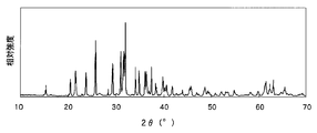
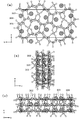
- Phosphor XRD profile with Sr 3 Si 13 Al 3 O 2 N 21 crystal structure Sr 3 Si 13 Al 3 O 2 N 21 illustrates the crystal structure.
- A) is a projection view in the a-axis direction
- (b) is a projection view in the b-axis direction
- (c) is a projection view in the c-axis direction.
- Sr 2 Si 7 Al 3 ON 13 shows the crystal structure.
- FIG. 1 is a projection view in the a-axis direction
- (b) is a projection view in the b-axis direction
- (c) is a projection view in the c-axis direction.
- FIG. 2 is an ESR spectrum of the phosphor according to Example 1.
- FIG. 2 The ESR spectrum of the phosphor according to Example 2.
- the ESR spectrum of the phosphor according to Example 3. The ESR spectrum of the phosphor according to Comparative Example 1.
- the ESR spectrum of the phosphor according to Comparative Example 2. The ESR spectrum of the phosphor according to Comparative Example 3.
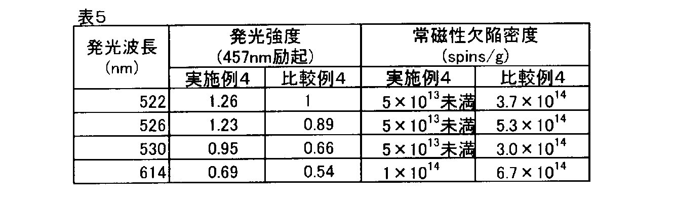
- FIG. The emission spectrum of the fluorescent substance by Example 4 and the comparative example 4.
- FIG. The ESR spectrum of the phosphor according to Example 4.
- the ESR spectrum of the phosphor according to Comparative Example 4. The emission spectrum of the fluorescent substance by Example 5 and Comparative Example 5.
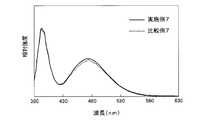
- FIG. The emission spectrum of the fluorescent substance by Example 7 and Comparative Example 7.
- the present inventors have found that a phosphor having high quantum efficiency and good temperature characteristics can be obtained by adding an emission center element to an oxynitride compound having a limited crystal structure and composition.
- One of the phosphors in the present invention includes a metal element M selected from a group IA element, a group IIA element, a group IIIA element excluding aluminum, a group IIIB element, a rare earth element, and a group IVA element excluding silicon, and aluminum.
- a metal element M selected from a group IA element, a group IIA element, a group IIIA element excluding aluminum, a group IIIB element, a rare earth element, and a group IVA element excluding silicon, and aluminum.
- the phosphor according to the present invention is based on the inorganic compound, and a part of the metal element M constituting the crystal structure is substituted with the emission center element R.
- the luminescent center element R is Eu, Ce, Mn, Tb, Yb, Dy, Sm, Tm, Pr, Nd, Pm, Ho, Er, Cr, Sn, Cu, Zn, As, Ag, Cd, Sb. , Au, Hg, Tl, Pb, Bi, and Fe.
- a sialon phosphor such a phosphor is sometimes referred to as a sialon phosphor because it contains Si, Al, O, and N.
- the metal element M is a group IA element such as Li, Na and K, a group IIA element such as Mg, Ca, Sr and Ba, a group IIIA element such as B, Ga and In, and a group IIIB such as Y and Sc. Preferred are those selected from group elements, rare earth elements such as Gd, La, and Lu, and group IVA elements such as Ge.
- the metal element M may be a single element or a combination of two or more elements.
- the phosphor in the present invention has a crystal structure based on these elements M, Al, Si, and O, and / or N, but it is necessary that a part of M is substituted with the luminescent center element R. It is.
- the luminescent center element R can be arbitrarily selected from the above-described elements as necessary, but considering the variability of the emission wavelength, it is preferable to use at least one of Eu and Mn. Most preferably, Eu is used.
- the luminescent center element R replaces at least 0.1 mol% of the element M.
- substitution amount is less than 0.1 mol%, it is difficult to obtain a sufficient light emitting effect.
- the luminescence center element R may replace the entire amount of the element M, but when the substitution amount is less than 50 mol%, a decrease in the light emission probability (concentration quenching) can be suppressed as much as possible.
- the phosphor according to the present invention emits light of various wavelengths depending on the structure and the type of the luminescent center element when excited with light having a wavelength of 250 to 500 nm due to the presence of the luminescent center element. .
- the phosphor according to the present invention is characterized by a very low paramagnetic defect density.
- sialon-based oxynitride phosphor with few paramagnetic defects achieves high luminous efficiency due to such structural features.
- Such a paramagnetic defect density can be measured by ESR. Specifically, it is performed by sweeping a magnetic field while irradiating a sample with microwaves. Since ESR is a spectroscopic analysis that observes transitions between levels that occur when unpaired electrons are placed in a magnetic field, the energy interval between levels that increases as the magnetic field increases, the energy of the microwave, However, absorption is observed when they are equal.
- the ESR spectrum is usually obtained by a differential curve, and when this differential curve is integrated once, an absorption curve is obtained, and when it is integrated twice, signal intensity is obtained.
- the oxynitride phosphor having a low paramagnetic defect density according to the present invention can be produced by any method. As such a method, for example, two-stage firing as described later can be cited. On the other hand, in a conventional manufacturing method by firing, the paramagnetic defect density is high, and it is difficult to achieve a low paramagnetic defect density as specified in the present invention.
- One embodiment of the phosphor according to the present invention has the same crystal structure as Sr 3 Si 13 Al 3 O 2 N 21, and emits light in a blue-green to yellow-green region when excited with light having a wavelength of 250 to 500 nm. That is, it is a green light emitting phosphor exhibiting light emission having a peak between wavelengths of 490 to 580 nm.
- Sr, Si, Al, O, or N which is a constituent element thereof is replaced with another element, or another metal element such as Eu is dissolved. By such replacement, the lattice constant changes, and the crystal structure may change slightly.
- the atomic position given by the crystal structure, the site occupied by the atoms, and the coordinates of the sites does not change so much that the chemical bond between the skeletal atoms is broken.
- the phosphor of the present invention can exhibit the effects of the present invention as long as the basic crystal structure does not change.
- the range in which such a basic crystal structure does not change can be defined as follows. That is, in the present invention, the lengths of the chemical bonds of M 1 -N and M 2 -N (distance between adjacent atoms) calculated from the lattice constant and atomic coordinates obtained by X-ray diffraction or neutron diffraction are expressed as follows.
- composition formula of the green light emitting phosphor is represented by the following general formula (1).
- M 1-x1 R x1 3-y1 Si 13-z Al 3 + z O 2 + u N 21-w
- M and R are as described above, 0 ⁇ x1 ⁇ 1, preferably 0.001 ⁇ x1 ⁇ 0.5, ⁇ 0.1 ⁇ y1 ⁇ 0.15, preferably ⁇ 0.09 ⁇ y1 ⁇ 0.07, ⁇ 1 ⁇ z ⁇ 1, preferably 0.2 ⁇ z ⁇ 1, ⁇ 1 ⁇ u ⁇ w ⁇ 1, preferably ⁇ 0.1 ⁇ u ⁇ w ⁇ 0.3.
- the green light-emitting phosphor according to an embodiment of the present invention is based on an inorganic compound having substantially the same crystal structure as Sr 3 Si 13 Al 3 O 2 N 21, and a part of the constituent elements is replaced with the light-emitting element. As the composition of each element is defined within a predetermined range, good quantum efficiency is exhibited.
- the crystal structure of the Sr 3 Al 3 Si 13 O 2 N 21 crystal is as shown in FIG.
- the green light emitting phosphor according to the present invention can be identified by X-ray diffraction or neutron diffraction. That is, in addition to the substance showing the same profile as the XRD profile of Sr 3 Si 13 Al 3 O 2 N 21 shown here, the lattice constants are changed within a certain range by replacing constituent elements with other elements Are also included in the green-emitting phosphor according to the present invention.
- the constituent element is replaced with another element when Sr in the Sr 3 Si 13 Al 3 O 2 N 21 crystal is the element M and / or the emission center element R, and the position of the element Si is a tetravalent element.
- Al and Si are replaced with each other, and O and N are replaced.
- Sr 3 Si 14 Al 2 ON 22 , Sr 3 Si 15 AlN 23 , Sr 3 Si 12 Al 4 O 3 N 20 , Sr 3 Si 11 Al 5 O 4 N 19 , Sr 3 Si 10 Al 6 O 5 N 18, etc. are also Sr 3 Si 13 Al 3 O 2 N 21 group crystals.
- the phosphor according to another embodiment of the present invention has the same crystal structure as Sr 2 Si 7 Al 3 ON 13 and has a peak between wavelengths 570 to 650 nm when excited with light having a wavelength of 250 to 500 nm. It is a red light emitting phosphor exhibiting light emission.
- This red-emitting phosphor is based on Sr 2 Si 7 Al 3 ON 13 and its constituent elements Sr, Si, Al, O, or N are replaced with other elements, or other metal elements such as Eu are used. It can also be said that it is a solid solution. However, as in the case of the green light-emitting phosphor described above, a slight change in crystal structure due to such replacement does not cause a problem. That is, in the present invention, the length of chemical bonds of Al—N and Si—N (distance between adjacent atoms) calculated from the lattice constant and atomic coordinates obtained by X-ray diffraction or neutron diffraction are shown in Table 2.
- the crystal structure changes when it is within ⁇ 15% of the length of the chemical bond of Al—N and Si—N calculated from the lattice constant and atomic coordinates of Sr 2 Si 7 Al 3 ON 13 shown Define that it is not.
- the phosphor according to the present invention has such a crystal structure. If the length of the chemical bond is changed beyond this range, the chemical bond is broken to form another crystal, and the effect of the present invention may be reduced.
- One of the red light-emitting phosphors according to the present invention is preferably represented by the following composition formula (2).
- M and R are as described above, 0 ⁇ x2 ⁇ 0.4, preferably 0.02 ⁇ x2 ⁇ 0.2, 0.65 ⁇ a ⁇ 0.70, preferably 0.66 ⁇ a ⁇ 0.69, 2 ⁇ b ⁇ 3, preferably 2.2 ⁇ b ⁇ 2.4, 0.3 ⁇ c ⁇ 0.6, preferably 0.43 ⁇ c ⁇ 0.51, 4 ⁇ d ⁇ 5, preferably 4.2 ⁇ d ⁇ 4.3.
- the red light-emitting phosphor according to an embodiment of the present invention is based on an inorganic compound having substantially the same crystal structure as Sr 2 Si 7 Al 3 ON 13, and a part of the constituent elements is substituted with the light-emitting element.
- the composition of each element is defined within a predetermined range. Good quantum efficiency is exhibited at this time, and preferable temperature characteristics are exhibited such that temperature quenching is small when used in a light-emitting element.
- This crystal belongs to the space group Pna21 (164th in the space group shown in Non-Patent Document 1). Note that the crystal space group can be determined by single crystal XRD.
- the crystal structure of the Sr 2 Si 7 Al 3 ON 13 crystal is as shown in FIG.
- the phosphor according to the present invention can be identified by X-ray diffraction or neutron diffraction. That is, in addition to the material showing the same profile as the XRD profile of Sr 2 Si 7 Al 3 ON 13 shown here, a material whose lattice constant is changed in a certain range by replacing the constituent element with another element is It is included in the phosphor according to the invention.
- the constituent element is replaced by another element means that Sr in the Sr 2 Si 7 Al 3 ON 13 crystal is the element M and / or the emission center element R, and the position of the element Si is a tetravalent element.
- Group for example, one or more elements selected from the group consisting of Ge, Sn, Ti, Zr, and Hf, and a group in which the position of Al is a trivalent element, for example, B, Ga, In, Sc, Y One or more elements selected from the group consisting of La, Gd, and Lu, and the position of O or N is substituted with one or more elements selected from the group consisting of O, N, and C Crystal.
- Al is simultaneously replaced with each other to Si, O and N are replaced, for example, Sr 2 Si 8 Al 2 N 14 , Sr 2 Si 6 Al 4 O 2 N 12, Sr 2 Si 5 A l5 O 3 N 11, Sr 2 Si 4 Al 6 O 4 N 10 and the like are also Sr 2 Si 7 Al 3 ON 13 group crystals.
- the Sr 2 Si 7 Al 3 ON 13 group crystal can be determined by the diffraction peak position of the XRD profile as in the case of the green light emitting phosphor.
- Another host in the phosphor according to the embodiment of the present invention is represented by the following general formula (3a), and is excited between 400 nm and 700 nm when excited with electron energy or light having a wavelength of 250 nm to 500 nm.
- Examples thereof include sialon compounds having an emission peak.
- Examples of the Group IIA metal that can be introduced as M ′ include Ba, Ca, Sr, and Mg. They may be used alone or in combination of two or more.
- Examples of rare earth metals that can be introduced as M ′ include Y, Gd, and La, and can be used alone or in combination of two or more. A combination of these Group IIA metals and rare earth metals can also be used.
- M ′ is a metal selected from the group consisting of Group IIA metals and rare earth metals, and p is a numerical value satisfying 0 ⁇ p ⁇ 10.
- the phosphor according to the embodiment of the present invention is obtained, for example, by replacing at least a part of the metal M ′ in the general formula (3) with an emission center element.
- a phosphor is represented by the following general formula (3).
- M ′ is a metal selected from the group consisting of Group IIA metals and rare earth metals
- R is a luminescent center element
- p and y are numerical values satisfying the following relations, respectively. 0 ⁇ p ⁇ 10, 0 ⁇ x3 ⁇ 1)
- the luminescent center element replaces at least 0.1 mol% of the metal M ′.
- the substitution amount is less than 0.1 mol%, it is difficult to obtain a sufficient light emitting effect.
- 100% of the Group IIA metal M ′ may be substituted with the luminescent center element. In this case, an effect that the efficiency is further increased can be obtained.
- the oxynitride phosphor having an AlN polytypoid structure in the present invention preferably contains 0.3 to 30% by weight of oxygen. Since the oxide becomes a liquid phase at a high temperature, the synthesis is promoted via the liquid phase of the oxide during the synthesis. When the amount is less than 0.3% by weight, the reactivity is lowered, and it is difficult to perform good synthesis. On the other hand, when oxygen is contained in a large amount exceeding 30% by weight, a polytypoid structure may no longer be obtained.
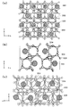
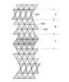
- the structure of the phosphor represented by the general formula (3) is schematically shown in FIG. 6 (see Non-Patent Document 2).
- the triangle represents a tetrahedral structure having Al or Si as the element 103 at the center of gravity and N or O as the element 102 at each vertex.
- Reference numeral 101 in the figure represents a Group IIA metal M ′.
- the phosphor represented by the above general formula (3) is a 12-coordinate layer centered on M ′ represented by A, a layer composed of regular tetrahedrons sharing a vertex with each other represented by B, C
- the layer is composed of a regular tetrahedron that shares a plane with each other, and the layer composed of a regular tetrahedron that shares a vertex with each other.
- the number of layers of the regular tetrahedron structure included in each layer of A, B, C, and D is not limited to the example of FIG.
- a periodic structure is a wurtzite structure in which the AlN 4 tetrahedral structure shares a vertex, and a SiN 4 structure and a 14-sided structure centered on M ′ are sandwiched in layers at the position 101.
- the phosphor has a lower luminous efficiency when the temperature rises (temperature quenching), but the phosphor according to the embodiment of the present invention has a feature that the luminous efficiency is less lowered when the temperature rises and the quenching temperature is high.
- Have Factors affecting temperature quenching include the difference in the size of the luminescent center ion and the size of the phosphor host ion that it replaces, the crystal lattice stability of the phosphor host, and the like.
- the sialon-based oxynitride phosphor according to the embodiment of the present invention is presumed to have a high quenching temperature due to the above-described crystal structure and low paramagnetic defect density.
- the present inventors considered as follows. That is, for example, in a nitride phosphor having an AlN 4 or SiN 4 regular tetrahedral structure as shown in FIG. 6 as a basic skeleton, the larger the number of shared tetrahedral vertices, the stronger and more stable the crystal lattice.
- the phosphor shown in FIG. 6 has a vertex sharing number of 2 to 6, and has four vertex sharing in the unit cell at four locations, four vertex sharing at about 60 locations, and six vertex sharing at about 24 locations.
- the average vertex sharing number is 2 to 3. Since the vertex sharing number is larger than that of the conventional phosphor, it is considered that the phosphor according to the embodiment of the present invention has a more stable crystal lattice.
- the presence of the emission center in the two-dimensional layered structure and the taking of the tetrahedral coordination structure also contributes to the stability around the emission center.
- the method for producing an oxynitride phosphor according to the present invention is for producing an oxynitride phosphor having the composition and crystal structure as described above.
- the target oxynitride phosphor in the present invention includes, for example, a nitride of element M or a carbide such as cyanamide, a nitride, an oxide, or a carbide of Al or Si, and an oxide of an emission center element R, It can be synthesized using nitrides or carbonates as starting materials.
- Sr 3 N 2 , AlN, Si 3 N 4 , Al 2 O 3 and EuN can be used as a starting material.
- Sr 3 N 2 , Ca 3 N 2 , Ba 3 N 2 , Sr 2 N, SrN, SrCO 3 or the like, or a mixture thereof may be used. These can be weighed and mixed so as to have a desired composition to obtain a raw material mixture.
- a technique of mixing a mortar in a glove box can be mentioned.
- the container to be used is not particularly limited, but an agate mortar is generally used.
- the raw material mixture can be obtained by ball mill mixing in a suitable solvent such as dehydrated isopropanol, ethanol, or water.
- a suitable solvent such as dehydrated isopropanol, ethanol, or water.
- the mixing time is not particularly limited and is, for example, 2 to 72 hours. In this case, it is common to volatilize and remove the solvent prior to firing.
- the obtained raw material mixture is dried or crushed as necessary, filled in a suitable container, and first fired in a nitrogen atmosphere to be an intermediate fired product.
- This firing step is hereinafter referred to as a first firing step.
- the reason why the first firing step is performed in a nitrogen atmosphere is to prevent excessive oxidation of raw materials such as aluminum nitride.
- a method is used in which after the raw material mixture is placed in the furnace, the pressure in the furnace is reduced, and then nitrogen is introduced to replace the gas in the furnace with nitrogen. it can.
- the raw material mixture may be accommodated in a container.
- the container can be covered with a powder that cannot enter or leave powder other than gas.
- this lid does not seal the container. In this way, by restricting the flow rate of the gas entering and leaving the container, it is possible to prevent the inside of the container from becoming unnecessarily high pressure.
- the firing treatment in the first firing step is generally performed at 1500 to 2000 ° C., preferably 1800 to 2000 ° C. If the firing temperature is less than 1500 ° C., it may be difficult to form the target phosphor. On the other hand, if it exceeds 2000 ° C., there is a risk of sublimation of the material or product.
- the firing time is generally 0.5 to 10 hours, preferably 2 to 6 hours.
- the nitrogen atmosphere is preferably performed at atmospheric pressure or higher, and more preferably at 5 atmospheric pressure or higher. This is because firing at high pressure can suppress decomposition of silicon nitride or the like at a high temperature.
- the obtained intermediate fired product is further subjected to the second firing step.
- firing is performed in a nitrogen-hydrogen mixed gas atmosphere. That is, the second firing step is performed in a reducing atmosphere.
- the content of hydrogen in the nitrogen-hydrogen mixed gas needs to be 1% or more and 100% or less, and preferably 30% or more and 90% or less.
- the firing treatment in the second firing step is generally performed at 1000 to 1900 ° C., preferably 1400 to 1800 ° C.
- the heating temperature in the second firing step is preferably lower than that in the first firing step.
- the firing time is generally 0.1 to 20 hours, preferably 0.5 to 12 hours.
- characteristics such as the emission intensity of the phosphor are improved. This is considered to be because crystal defects of the oxynitride phosphor are reduced, and according to the method of the present invention, a phosphor exhibiting characteristics completely different from those of a phosphor manufactured by firing in a conventional inert atmosphere. Can be obtained.
- the second baking step it is preferable to perform baking by storing the intermediate fired product in a shielded container.
- the obtained intermediate fired product is pulverized and accommodated in a lidded container, and the lidded container containing the intermediate fired product is further coated with an outer cover having an inner lid and an outer lid.
- the container is placed in a container, the outer container is placed in a furnace, the inside of the container is decompressed, a nitrogen-hydrogen mixed gas is introduced to replace the gas in the container, and then the second baking step is performed.
- a container with a lid for example, a general crucible can be used.
- shielding does not mean that the container is completely sealed. Oxynitride having an appropriate composition by preventing the pressure in the container from changing excessively by allowing the gas in and out of the container to be changed, and limiting the amount of hydrogen or nitrogen that reacts with the raw material A phosphor can be formed.
- the container filled with the raw material mixture or the intermediate fired product in the first firing process or the second firing process is not particularly limited.
- the material of the crucible and lid used as a container with a lid, or an outer container, an inner lid and an outer lid should be boron nitride, silicon nitride, silicon carbide, carbon, aluminum nitride, sialon, aluminum oxide, molybdenum or tungsten. Can do.
- the phosphor according to the embodiment can be obtained by subjecting the fired powder to post-treatment such as washing as necessary.
- washing for example, pure water washing or acid washing can be performed.
- the phosphor manufactured by the method of the present invention can be applied not only to LEDs that emit green, red, and blue light but also to white LEDs.
- white light can be obtained by using a combination of a plurality of types of phosphors that emit light of other wavelengths in the aforementioned phosphor.
- a plurality of phosphors that emit red, yellow (or green), and blue light by ultraviolet light can be used in combination.
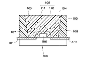
- FIG. 1 shows a cross section of a light emitting device using a phosphor according to an embodiment of the present invention.
- the light-emitting device includes a light-emitting element that emits light having a wavelength of 250 nm to 500 nm, and a phosphor layer that is disposed on the light-emitting element and includes a phosphor according to an embodiment of the present invention.
- the resin stem 100 includes a lead 101 and a lead 102 formed by molding a lead frame, and a resin portion 103 formed integrally therewith.
- the resin portion 103 has a concave portion 105 whose upper opening is wider than the bottom surface portion, and a reflective surface 104 is provided on a side surface of the concave portion.
- a light emitting chip 106 is mounted with Ag paste or the like at the center of the substantially circular bottom surface of the recess 105.
- the light emitting chip 106 for example, a light emitting diode, a laser diode, or the like can be used.
- emits an ultraviolet light can be used, It does not specifically limit.
- chips capable of emitting light of wavelengths such as blue, blue-violet, and near ultraviolet light can also be used.
- a GaN-based semiconductor light emitting element or the like can be used.
- the electrodes (not shown) of the light emitting chip 106 are connected to the leads 101 and 102 by bonding wires 107 and 108 made of Au or the like, respectively. The arrangement of the leads 101 and 102 can be changed as appropriate.
- a fluorescent layer 109 is disposed in the recess 105 of the resin portion 103.
- the phosphor layer 109 can be formed by dispersing or precipitating the phosphor 110 according to the embodiment of the present invention at a rate of 5 wt% to 50 wt% in a resin layer 111 made of, for example, a silicone resin. .
- a resin layer 111 made of, for example, a silicone resin.
- oxynitride having high covalent bond is used as a base material.
- the phosphor according to the present invention is generally hydrophobic and has very good compatibility with the resin. Therefore, scattering at the interface between the resin and the phosphor is remarkably suppressed, and the light extraction efficiency is improved.
- an n-type substrate may be used for the light emitting chip 106 to have the following configuration. Specifically, an n-type electrode is formed on the back surface of the n-type substrate, a p-type electrode is formed on the upper surface of the semiconductor layer on the substrate, and the n-type electrode or the p-type electrode is mounted on a lead. The p-type electrode or the n-type electrode can be connected to the other lead by a wire.
- the size of the light emitting chip 106 and the size and shape of the recess 105 can be changed as appropriate.
- the light emitting device is not limited to the package cup type as shown in FIG. Specifically, in the case of a bullet-type LED or a surface-mounted LED, the same effect can be obtained by applying the phosphor of the embodiment.
- Example 1 Sr 3 N 2 , EuN, Si 3 N 4 , Al 2 O 3 and AlN were prepared as starting materials. Each of these 2.500 g, 0.647 g, 5.987 g, 0.748 g, and 0.710 g was weighed in a vacuum glove box filled with Ar and then dry mixed in an agate mortar into a boron nitride crucible. Filled and fired at 1850 ° C. for 4 hours in N 2 atmosphere at 7.5 atm. The design composition is (Sr 0.87 Eu 0.13 ) 3 Si 12.8 Al 3.2 O 2.2 N 20 An intermediate fired product of .8 was obtained. Since the obtained intermediate baked product is a powder having a yellowish green color and is itself a phosphor, green light emission was observed when excited with black light.
- This intermediate baked product is filled in a boron nitride crucible with a lid, that is, a container with a lid, and this lidded container is stored in a boron nitride crucible that is slightly larger than that, that is, an outer container, and then the lid is closed.
- the phosphor was obtained by firing at 1500 ° C. for 12 hours in a 1 atm N 2 / H 2 atmosphere. At this time, an outer jacket having an inner lid and an outer lid was used.
- Example 2 Sr 3 N 2 , EuN, Si 3 N 4 , Al 2 O 3 and AlN were prepared as starting materials. Each of these 2.356 g, 0.896 g, 5.987 g, 0.748 g, and 0.710 g was weighed in a vacuum glove box filled with Ar, and then dry-mixed in an agate mortar and filled into a boron nitride crucible. Then, it is fired at 1850 ° C. for 4 hours in a N 2 atmosphere at 7.5 atm, and the designed composition is (Sr 0.82 Eu 0.18 ) 3 Si 12.8 Al 3.2 O 2.2 N 20. An intermediate fired product of 8 was obtained. The obtained intermediate fired product was a powder having a yellowish green color, and as a result of excitation with black light, green light emission was observed.
- This intermediate fired product was stored in a container in the same manner as in Example 1 and fired at 1500 ° C. for 12 hours in a 1 atm N 2 / H 2 atmosphere to obtain a phosphor.
- Example 3 Sr 3 N 2 , EuN, Si 3 N 4 , Al 2 O 3 and AlN were prepared as starting materials. Each of these 2.155 g, 1.244 g, 5.987 g, 0.748 g, and 0.710 g was weighed in a vacuum glove box filled with Ar, and then dry-mixed in an agate mortar and filled into a boron nitride crucible. And calcined at 1850 ° C. for 4 hours in a N 2 atmosphere of 7.5 atm, and the design composition is (Sr 0.75 Eu 0.25 ) 3 Si 12.8 Al 3.2 O 2.2 N 20. An intermediate fired product of 8 was obtained. The obtained intermediate fired product was a powder having a yellowish green color, and as a result of excitation with black light, green light emission was observed.
- This intermediate fired product was stored in the same manner as in Example 1 and fired at 1500 ° C. for 12 hours in a 1 atm N 2 / H 2 atmosphere to obtain a phosphor.
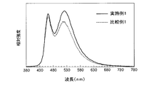
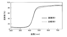
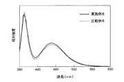
- Emission intensity is normalized based on the emission intensity of the comparative example at each emission wavelength.
- Comparative Example 1 has a lower reflectance in the vicinity of 500 to 550 nm than Example 1, and it can be seen that the phosphor itself absorbs yellow-green light emission.
- the reason why the emission intensity of the comparative example is low is considered to be absorption by the phosphor itself, and this light absorption is considered to be caused by nitrogen defects detected by ESR.
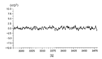
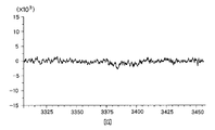
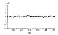
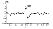
- the ESR spectra of the phosphors of Examples 1 to 3 and Comparative Examples 1 to 3 were as shown in FIGS. 11 to 16, respectively.
- the paramagnetic defect density of the phosphors of Examples 1 to 3 was less than the detection limit (5.0 ⁇ 10 13 spins / g), whereas the phosphors of Comparative Examples 1 to 3 had a paramagnetic density of around 2.0023. Magnetic spin was detected.
- the paramagnetic defect densities determined from the ESR spectra of the phosphors of Examples 1 to 3 and Comparative Examples 1 to 3 are as shown in Table 3. It is considered that the permanent defect detected in the comparative example is derived from nitrogen deficiency.
- Example 4 Sr 3 N 2 , EuN, Si 3 N 4 , Al 2 O 3 and AlN were prepared as starting materials. Each of these 2.472 g, 0.747 g, 4.911 g, 0.510 g, and 1.435 g was weighed in a vacuum glove box filled with Ar, and then dry mixed in an agate mortar and filled into a boron nitride crucible. Then, it was baked at 1850 ° C. for 4 hours in a N 2 atmosphere at 7.5 atm to synthesize a phosphor having a design composition of (Sr 0.85 Eu 0.15 ) 2 Si 7 Al 3 ON 13 .
- the fired phosphor was an orange powder, and red light emission was observed as a result of excitation with black light.
- the phosphor was filled in a boron nitride crucible with a lid, and the crucible was stored in a boron nitride crucible that was slightly larger than the crucible, and the lid was placed in a 1 atm N 2 / H 2 atmosphere. And baked at 1650 ° C. for 0.5 hour.
- the fired phosphor was an orange powder, and red light emission was observed as a result of excitation with black light.
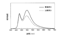
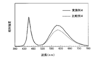
- the emission spectra of the phosphors of Example 4 and Comparative Example 4 with excitation light having a wavelength of 457 nm were as shown in FIG. Further, the emission characteristics of the phosphors of Example 4 and Comparative Example 4 were as shown in Table 5. * Emission intensity is normalized based on the emission intensity in the comparative example.
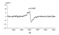
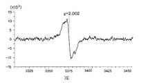
- FIG. 19 and 20 show the ESR spectra of the orange powders of Example 4 and Comparative Example 4, respectively.
- the orange powder of Comparative Example 4 detected a large amount of paramagnetic defects having a g of about 2.002, while the detected amount from the orange powder of Example 4 was small.
- the paramagnetic defect density by ESR of the orange powders of Example 4 and Comparative Example 4 is also shown in Table 5. It is considered that the permanent defect detected in Comparative Example 4 is derived from nitrogen deficiency.
- Example 5 SrCO 3 , Eu 2 O 3 , Si 3 N 4 and AlN were prepared as starting materials. Each of these 0.664 g, 0.792 g, 3.788 g, and 7.009 g was weighed and then dry mixed in an agate mortar and filled in a boron nitride crucible at 1800 ° C. in an N 2 atmosphere of 7 atm. After firing for 4 hours, a phosphor having a design composition of (Sr 0.5 Eu 0.5 ) Si 9 Al 19 ON 31 was synthesized.
- the fired phosphor was a light green powder, and as a result of excitation with black light, blue light emission was observed.
- the phosphor was filled in a boron nitride crucible with a lid, and the crucible was stored in a boron nitride crucible that was slightly larger than the crucible, and the lid was placed in a 1 atm N 2 / H 2 atmosphere. And baked at 1650 ° C. for 0.5 hour.
- the fired phosphor was a light green powder, and as a result of excitation with black light, blue light emission was observed.
- Example 6 SrCO 3 , Eu 2 O 3 , Si 3 N 4 and AlN were prepared as starting materials. Each of these 0.332 g, 1.188 g, 3.788 g, and 7.009 g was weighed and then dry mixed in an agate mortar and filled in a boron nitride crucible at 7800 N 2 atmosphere at 1800 ° C. After firing for 4 hours, a phosphor having a design composition of (Sr 0.25 Eu 0.75 ) Si 9 Al 19 ON 31 was synthesized.
- the fired phosphor was a light green powder, and as a result of excitation with black light, blue light emission was observed.
- the phosphor was filled in a boron nitride crucible with a lid, and the crucible was stored in a boron nitride crucible that was slightly larger than the crucible, and the lid was placed in a N 2 / H 2 atmosphere at 1 atm. Baked at 1650 ° C. for 0.5 hour.
- the fired phosphor was a light green powder, and as a result of excitation with black light, blue light emission was observed.
- Example 7 Eu 2 O 3 , Si 3 N 4 and AlN were prepared as starting materials. After weighing each 1.584 g, 3.788 g, and 7.009 g, these were dry-mixed in an agate mortar, filled in a boron nitride crucible, and baked at 1800 ° C. for 4 hours in a 7 atmosphere N 2 atmosphere. Thus, a phosphor having a design composition of EuSi 9 Al 19 ON 31 was synthesized.
- the fired phosphor was a light green powder, and as a result of excitation with black light, blue light emission was observed.
- the phosphor was filled in a boron nitride crucible with a lid, and the crucible was stored in a boron nitride crucible that was slightly larger than the crucible, and the lid was placed in a 1 atm N 2 / H 2 atmosphere. And baked at 1650 ° C. for 0.5 hour.
- Comparative Example 7 Eu 2 O 3 , Si 3 N 4 and AlN were prepared as starting materials. After weighing each 1.584 g, 3.788 g, and 7.009 g, these were dry-mixed in an agate mortar, filled in a boron nitride crucible, and baked at 1800 ° C. for 4 hours in a 7 atmosphere N 2 atmosphere. Thus, a phosphor having a design composition of EuSi 9 Al 19 ON 31 was synthesized.
- the fired phosphor was a light green powder, and as a result of excitation with black light, blue light emission was observed.
- Example 8 Ca 3 N 2 , EuN, Si 3 N 4 and AlN were prepared as starting materials. Each of these 3.744 g, 0.204 g, 2.869 g, and 3.274 g was weighed in a vacuum glove box filled with Ar, and then dry-mixed in an agate mortar, and filled into a boron nitride crucible. A phosphor having a design composition of (Ca 0.984 Eu 0.016 ) SiAlN 3 was synthesized by firing at 1850 ° C. for 4 hours in an N 2 atmosphere of 5 atm.
- the fired phosphor was a powder with a red body color, and red light emission was observed as a result of excitation with black light.
- the phosphor was filled in a boron nitride crucible with a lid, and the crucible was stored in a boron nitride crucible that was slightly larger than the crucible, and the lid was placed in a 1 atm N 2 / H 2 atmosphere. Firing was carried out at 1500 ° C. for 12 hours.
- Comparative Example 8 Ca 3 N 2 , EuN, Si 3 N 4 and AlN were prepared as starting materials. Each of these 3.744 g, 0.204 g, 2.869 g, and 3.274 g was weighed in a vacuum glove box filled with Ar, and then dry-mixed in an agate mortar, and filled into a boron nitride crucible. A phosphor having a design composition of (Ca 0.984 Eu 0.016 ) SiAlN 3 was synthesized by firing at 1850 ° C. for 4 hours in an N 2 atmosphere of 5 atm.
- the fired phosphor was a powder with a red body color, and red light emission was observed as a result of excitation with black light.
- the emission spectra of the phosphors of Example 8 and Comparative Example 8 at 455 nm excitation are as shown in FIG. Further, the emission intensity of the phosphor of Example 8 at 660 nm when excited with light having a wavelength of 455 nm was 1.10 times that of the phosphor of Comparative Example 8.
Abstract
[課題]量子効率が高く、温度特性の良好な蛍光体と、その製造方法の提供。 [解決手段]金属元素Mと、アルミニウムと、ケイ素と、OおよびNの一方または両方を含む組成を有する無機化合物の、金属元素Mの一部が発光中心元素Rにより置換された、常磁性欠陥密度の低いサイアロン系酸窒化物蛍光体。この蛍光体は、原料混合物を窒素雰囲気中で熱処理して中間焼成物を得て、さらにその中間焼成物を窒素水素混合気体雰囲気中で熱処理することにより得ることができる。
Description
本発明は、発光装置に使用される蛍光体の製造方法およびそれにより製造された蛍光体に関するものである。特に、電界放出型ディスプレイ等のディスプレイ、および青色発光ダイオードまたは紫外発光ダイオードを光源とする発光装置に使用することができる蛍光体に関するものである。
発光ダイオードを用いたLEDランプは、携帯機器、PC周辺機器、OA機器、各種スイッチ、バックライト用光源、および表示板などの各種表示装置に用いられている。これらLEDランプは高効率化が強く望まれており、加えて一般照明用途には高演色化、バックライト用途には高色域化の要請がある。高効率化には、蛍光体の高効率化が必要であり、高演色化あるいは高色域化には青色光で励起された場合に緑色の発光を示す蛍光体が有用である。
また、高負荷LEDは駆動により発熱し、蛍光体の温度が100~200℃程度まで上昇することが一般的である。、このような温度上昇が起こると蛍光体の発光強度は一般に低下する。このため蛍光体は、温度が上昇した場合であっても発光強度の低下が少ないことが望まれている。
かかるLEDランプに用いるのに適当な、青色光で励起された場合に緑色の発光を示す蛍光体の例としてEu付活βサイアロン蛍光体が挙げられる(例えば特許文献1)。この蛍光体は450nm励起で効率がよいとされ、450nm励起では、吸収率65%、内部量子効率53%、発光効率35%程度の性能を有するものである。
また、昨今、フラットパネルディスプレイ装置に関する開発はが精力的に行われ、その開発はPDP(プラズマディスプレイ)やLCD(液晶ディスプレイ)に重点が置かれている。しかしながら、より鮮明な画像を提供するという点でPDPやLCDを凌駕するものとして、電界放出型ディスプレイが期待されている。
電界放出型ディスプレイは、赤色、緑色、および青色の蛍光体が配列されたスクリーンと、このスクリーンに対してCRTよりも狭い間隔で対向するカソードを備えている。カソードには電子源がエミッタ素子として複数配置され、その近傍に配置されたゲート電極との電位差に応じて電子を放出する。放出された電子は蛍光体側のアノード電圧(加速電圧)により加速されて蛍光体に衝突して、これにより蛍光体が発光し、鮮明な画像を表示することができる。
かかる構成の電界放出型ディスプレイに使用される蛍光体としては、十分に高い発光効率を有し、高電流密度の励起において飽和に至った際にも、十分に高い発光効率を示すことが要求される。このような点のみに着目すれば、これまでCRT用蛍光体に用いられてきた硫化物系蛍光体(ZnS:Cu、ZnS:Agなど)も、この候補と考えられる。しかしながら、低エネルギー陰極線ディスプレイスクリーンの励起条件下では、ZnSのような硫化物系蛍光体は分解することが報告されている。この分解物は電子線を放出する熱フィラメントを著しく劣化させてしまうという問題点がある。特に、従来用いられているZnS系青色蛍光体は、赤色蛍光体および緑色蛍光体に比して輝度劣化が著しい傾向があるため、カラー画面の表示色が経時変化してしまうという問題が生じている。
また、本発明者らは、青色発光が可能なサイアロン系酸窒化物蛍光体を検討した(特許文献2)。この蛍光体は、従来の青色発光蛍光体に対して温度上昇による輝度低下が少ないものである。しかしながら、このような蛍光体よりもさらなる優れた特性をもつ蛍光体が望まれ、また青色発光以外の蛍光体についても、経時劣化を改良することが望まれていた。
International Tables for Crystallography, Volume A: Space-group symmetry, T. Hahn編,Springer(オランダ国)発行
J.Grins,S.Esmaeilzadeh,G.Svensson,Z.J.Shen, J.Euro.Cera.Soc. 19,2723(1999)
本発明は、前記したような従来の問題点に鑑みて、量子効率が高く、かつ温度特性の良好な蛍光体を製造する方法、およびそれにより製造された蛍光体を提供することを目的とするものである。
本発明の一実施態様にかかる酸窒化物蛍光体の製造方法は、IA族元素、IIA族元素、アルミニウムを除くIIIA族元素、IIIB族元素、希土類元素、およびケイ素を除くIVA族元素から選択される金属元素Mと、アルミニウムと、ケイ素と、酸素および窒素の一方または両方を含む組成を有し、前記金属元素Mの一部が、Eu、Ce、Mn、Tb、Yb、Dy、Sm、Tm、Pr、Nd、Pm、Ho、Er、Cr、Sn、Cu、Zn、As、Ag、Cd、Sb、Au、Hg、Tl、Pb、Bi、およびFeからなる群から選ばれる発光中心元素Rにより置換されている、酸窒化物蛍光体の製造方法であって、原料混合物を窒素雰囲気中で熱処理して中間焼成物を得る第一焼成工程、および前記中間焼成物を水素濃度1%以上100%以下の窒素水素混合気体雰囲気中で熱処理して、窒化物蛍光体を形成させる第二焼成工程を有することを特徴とするものである。
また、本発明の一実施態様による酸窒化物蛍光体は、IA族元素、IIA族元素、アルミニウムを除くIIIA族元素、IIIB族元素、希土類元素、およびケイ素を除くIVA族元素から選択される金属元素Mと、アルミニウムと、ケイ素と、酸素および窒素の一方または両方を含む組成を有し、Sr3Si13Al3O2N21と同一の結晶構造を有し、前記金属元素Mの一部が、Eu、Ce、Mn、Tb、Yb、Dy、Sm、Tm、Pr、Nd、Pm、Ho、Er、Cr、Sn、Cu、Zn、As、Ag、Cd、Sb、Au、Hg、Tl、Pb、Bi、およびFeからなる群から選ばれる発光中心元素Rにより置換されており、電子スピン共鳴で測定した際に、g=2.002に検出される常磁性欠陥密度が 2×10¹⁴spins/g未満であることを特徴とするものである。
本発明によれば、量子効率が高く、発光強度の高い蛍光体が提供される。これら蛍光体は、温度が上昇した場合であっても発光強度の低下が抑制されており、実用性がきわめて高いものである。
本発明者らは、結晶構造および組成を限定した酸窒化物化合物に発光中心元素を添加することによって、量子効率が高く温度特性の良好な蛍光体が得られることを見出した。本発明における蛍光体の1つは、IA族元素、IIA族元素、アルミニウムを除くIIIA族元素、IIIB族元素、希土類元素、およびケイ素を除くIVA族元素から選択される金属元素Mと、アルミニウムと、ケイ素と、酸素および窒素の一方または両方を含む組成を有する無機化合物を基本とする。そして、本発明による蛍光体は、その無機化合物を基本とし、その結晶構造を構成する金属元素Mの一部が、発光中心元素Rにより置換されている。ここで、発光中心元素Rは、Eu、Ce、Mn、Tb、Yb、Dy、Sm、Tm、Pr、Nd、Pm、Ho、Er、Cr、Sn、Cu、Zn、As、Ag、Cd、Sb、Au、Hg、Tl、Pb、Bi、およびFeから選ばれる元素である。以下、このような蛍光体は、Si、Al、O、およびNを含むことからサイアロン系蛍光体と呼ばれることがある。
金属元素Mは、Li、Na、およびK等のIA族元素、Mg、Ca、Sr、およびBa等のIIA族元素、B、Ga、およびIn等のIIIA族元素、Y、およびSc等のIIIB族元素、Gd、La、およびLu等の希土類元素、ならびにGe等のIVA族元素から選ばれるものが好ましい。金属元素Mは、一種類の元素であっても、または2種類以上の元素が組み合わされていてもよい。
本発明における蛍光体は、これらの元素M、Al、Si、ならびにO、および/またはNを基本とする結晶構造を有するが、Mの一部が発光中心元素Rに置換されていることが必要である。
発光中心元素Rとしては、前記した元素から必要に応じて任意に選択することができるが、発光波長の可変性等を考慮すると、これらのうち、EuおよびMnの少なくとも1種を用いることが好ましく、Euを用いることが最も好ましい。
発光中心元素Rは、元素Mの少なくとも0.1モル%を置換することが望ましい。置換量が0.1モル%未満の場合には、十分な発光効果を得ることが困難となる。発光中心元素Rは、元素Mの全量を置き換えてもよいが、置換量が50モル%未満の場合には、発光確率の低下(濃度消光)を極力抑制することができる。そして、本発明による蛍光体は、この発光中心元素の存在によって、波長250~500nmの光で励起した際、その構造や発光中心元素の種類に応じて、種々の波長の発光を示すものである。
本発明による蛍光体は、常磁性欠陥密度が非常に低いことを特徴とする。具体的には、本発明による蛍光体は、電子スピン共鳴(以下、ESRという)により測定した場合に、g=2.002で検出される常磁性欠陥密度が 2×10¹⁴spins/g未満、好ましくは5×1013spins/g未満であることを特徴としている。すなわち、サイアロン系蛍光体のような多元系蛍光体では一般に常磁性欠陥が生じやすい。これは、結晶構造中のNとOとの置換、あるいはAlとSiとの置換が起こってサイアロン系酸窒化物が形成されるときに置換が十分にできず、そのために欠陥が生じるものと考えられる。したがって、本発明において特定されるような常磁性欠陥が少ないサイアロン系酸窒化物はこれまでに得られていなかった。そして本発明による常磁性欠陥が少ないサイアロン系酸窒化物蛍光体は、そのような構造上の特徴によって高い発光効率を達成しているのである。
このような常磁性欠陥密度はESRにより測定できるが、具体的には、試料にマイクロ波を照射下しながら、磁場を掃引して行う。ESRは、不対電子が磁場中に置かれた時に生じる、準位間の遷移を観測する分光分析であるため、磁場が大きくなるに従って増大する準位間のエネルギー間隔と、マイクロ波のエネルギーとが、等しくなった時に吸収が観測される。ESRスペクトルは通常微分曲線で得られ、この微分曲線を一回積分すると吸収曲線、二回積分すると信号強度が得られる。
本発明による常磁性欠陥密度が低い酸窒化物蛍光体は、任意の方法で製造することができる。そのような方法としては、例えば、後述するような2段階焼成などが挙げられる。一方で従来行われていた、一般的な焼成による製造方法では常磁性欠陥密度は高くなり、本発明で特定されるような低い常磁性欠陥密度を達成することは困難である。
本発明による蛍光体の一実施態様は、Sr3Si13Al3O2N21と同一の結晶構造を有し、波長250~500nmの光で励起した際、青緑色から黄緑色にわたる領域の発光、すなわち波長490~580nmの間にピークを有する発光を示す緑色発光蛍光体である。この蛍光体は、その構成元素であるSr、Si、Al、O、またはNが他の元素に置き換えられたり、Euなどのほかの金属元素が固溶したものであるということもできる。このような置き換え等によって、格子定数は変化し、結晶構造が若干変化することがある。しかし、結晶構造と原子が占めるサイトとその座標によって与えられる原子位置は、骨格原子間の化学結合が切れるほどには大きく変わることは少ない。本発明の蛍光体は、基本的な結晶構造が変化しない範囲で本発明の効果を奏することができる、このような基本的な結晶構造が変化しない範囲は以下のように定義することができる。すなわち、本発明においては、X線回折や中性子線回折により求めた格子定数および原子座標から計算されたM1-NおよびM2-Nの化学結合の長さ(近接原子間距離)が、表1に示すSr3Si13Al3O2N21の格子定数と原子座標から計算されたAl-NおよびSi-Nの化学結合の長さに比べて、それぞれ±15%以内であるときに結晶構造が変化していないと定義する。本発明による緑色発光蛍光体はこのような結晶構造を有するものである。この範囲を超えて化学結合の長さが変化すると、その化学結合が切れて別の結晶となり、本発明による効果が小さくなることがある。
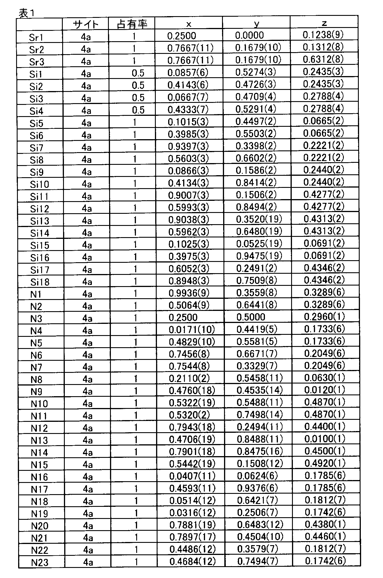
このような、本発明の一実施態様による緑色発光蛍光体の組成式は、下記一般式(1)で示されるものである。
(M1-x1Rx1)3-y1Si13-zAl3+zO2+uN21-w (1)
式中、MおよびRは前記したとおりであり、
0<x1≦1、好ましくは0.001≦x1≦0.5、
-0.1≦y1≦0.15、好ましくは-0.09≦y1≦0.07、
-1≦z≦1、好ましくは0.2≦z≦1、
-1<u-w≦1、好ましくは-0.1≦u-w≦0.3、である。
(M1-x1Rx1)3-y1Si13-zAl3+zO2+uN21-w (1)
式中、MおよびRは前記したとおりであり、
0<x1≦1、好ましくは0.001≦x1≦0.5、
-0.1≦y1≦0.15、好ましくは-0.09≦y1≦0.07、
-1≦z≦1、好ましくは0.2≦z≦1、
-1<u-w≦1、好ましくは-0.1≦u-w≦0.3、である。
本発明の一実施態様による緑色発光蛍光体は、Sr3Si13Al3O2N21と実質的に同一の結晶構造を有する無機化合物を基本とし、その構成元素の一部が発光元素に置換されたものであり、各元素の組成が所定の範囲内に規定されていることによって、良好な量子効率を示す。
Sr3Si13Al3O2N21結晶は斜方晶系で、格子定数は、a=9.037(6)Å、b=14.734(9)Å、c=14.928(10)Åであり、図2に示すXRDプロファイルを呈する。この結晶は空間群P212121(非特許文献1に示された空間群のうちの19番目)に属する。なお、結晶の空間群は単結晶XRDにより決定することができる。Sr3Al3Si13O2N21結晶の結晶構造は図3に示す通りである。
本発明による緑色発光蛍光体は、X線回折や中性子回折により同定することができる。すなわち、ここで示されるSr3Si13Al3O2N21のXRDプロファイルと同一のプロファイルを示す物質の他に、構成元素が他の元素に入れ替えられることにより格子定数が一定範囲で変化したものも、本発明による緑色発光蛍光体に包含されるものである。ここで、構成元素が他の元素で置き換わるものとは、Sr3Si13Al3O2N21結晶中のSrが元素Mおよび/または発光中心元素Rで、元素Siの位置が4価の元素からなる群、例えばGe、Sn、Ti、Zr、Hfからなる群から選ばれる1種または2種以上の元素で、Alの位置が3価の元素からなる群、例えばB、Ga、In、Sc、Y、La、Gd、Luからなる群から選ばれる1種または2種以上の元素で、OまたはNの位置がO、N、Cからなる群から選ばれる1種または2種以上の元素で置換された結晶のことである。また、AlがSiに互いに置き換えられると同時に、OとNが置き換えられた、例えばSr3Si14Al2ON22、Sr3Si15AlN23、Sr3Si12Al4O3N20、Sr3Si11Al5O4N19、Sr3Si10Al6O5N18等もSr3Si13Al3O2N21属結晶である。
さらに、固溶量が小さい場合には、Sr3Si13Al3O2N21属結晶の簡便な判定方法として次の方法がある。新たな物質について測定したXRDプロファイルの回折ピーク位置が主要ピークについて一致した時に、当該結晶構造が同じものと特定することができる。主要ピークとしては、回折強度の強い10本程度で判断すると良い。
本発明における別の実施態様である蛍光体は、Sr2Si7Al3ON13と同一の結晶構造を有し、波長250~500nmの光で励起した際に波長570~650nmの間にピークを有する発光を示す赤色発光蛍光体である。
この赤色発光蛍光体は、Sr2Si7Al3ON13をベースとして、その構成元素であるSr、Si、Al、O、またはNが他の元素で置き換わったり、Euなどのほかの金属元素が固溶したものであるということもできる。しかしながら、前記した緑色発光蛍光体の場合と同様、このような置き換え等による僅かな結晶構造の変化は問題とならない。すなわち、本発明においては、X線回折や中性子線回折により求めた格子定数および原子座標から計算されたAl-NおよびSi-Nの化学結合の長さ(近接原子間距離)が、表2に示されるSr2Si7Al3ON13の格子定数と原子座標から計算されたAl-NおよびSi-Nの化学結合の長さに比べて、それぞれ±15%以内であるときに結晶構造が変化していないと定義する。本発明による蛍光体はこのような結晶構造を有するものである。この範囲を超えて化学結合の長さが変化すると、その化学結合が切れて別の結晶となり、本発明による効果が小さくなることがある。
このような、本発明による赤色発光蛍光体のひとつは、下記組成式(2)で示されるものが好ましい。
(M1-x2Rx2)aSibAlOcNd (2)
(1)中、MおよびRは前記した通りであり、
0<x2<0.4、好ましくは0.02≦x2≦0.2、
0.65<a<0.70、好ましくは0.66≦a≦0.69、
2<b<3、好ましくは2.2≦b≦2.4、
0.3<c<0.6、好ましくは0.43≦c≦0.51、
4<d<5、好ましくは4.2≦d≦4.3である。
(M1-x2Rx2)aSibAlOcNd (2)
(1)中、MおよびRは前記した通りであり、
0<x2<0.4、好ましくは0.02≦x2≦0.2、
0.65<a<0.70、好ましくは0.66≦a≦0.69、
2<b<3、好ましくは2.2≦b≦2.4、
0.3<c<0.6、好ましくは0.43≦c≦0.51、
4<d<5、好ましくは4.2≦d≦4.3である。
本発明の一実施態様による赤色発光蛍光体は、Sr2Si7Al3ON13と実質的に同一の結晶構造を有する無機化合物を基本とし、その構成元素の一部が発光元素に置換されたものであり、各元素の組成が所定の範囲内に規定されている。このときに良好な量子効率を示し、発光素子に用いられたときに温度消光が小さいという好ましい温度特性を示す。
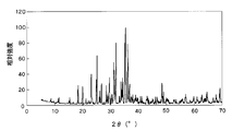
Sr2Al3Si7ON13結晶は斜方晶系で、格子定数は、a=11.8033(13)Å、b=21.589(2)Å、c=5.0131(6)Åであり、図4に示すXRDプロファイルを呈する。この結晶は空間群Pna21(非特許文献1に示された空間群のうちの164番目)に属する。なお、結晶の空間群は単結晶XRDにより決定することができる。Sr2Si7Al3ON13結晶の結晶構造は図5に示す通りである。
本発明による蛍光体は、X線回折や中性子回折により同定することができる。すなわち、ここで示されるSr2Si7Al3ON13のXRDプロファイルと同一のプロファイルを示す物質の他に、構成元素が他の元素と入れ替わることにより格子定数が一定範囲で変化したものも、本発明による蛍光体に包含されるものである。ここで、構成元素が他の元素で置き換わるものとは、Sr2Si7Al3ON13結晶中のSrが元素Mおよび/または発光中心元素Rで、元素Siの位置が4価の元素からなる群、例えばGe、Sn、Ti、Zr、Hfからなる群から選ばれる1種または2種以上の元素で、Alの位置が3価の元素からなる群、例えばB、Ga、In、Sc、Y、La、Gd、Luからなる群から選ばれる1種または2種以上の元素で、OまたはNの位置がO、N、Cからなる群から選ばれる1種または2種以上の元素で置換された結晶のことである。また、AlがSiに互いに置き換わると同時に、OとNが置き換わった、例えばSr2Si8Al2N14、Sr2Si6Al4O2N12、Sr2Si5Al5O3N11、Sr2Si4Al6O4N10等もSr2Si7Al3ON13属結晶である。
さらに、固溶量が小さい場合には、緑色発光蛍光体の場合と同様に、XRDプロファイルの回折ピーク位置によって、Sr2Si7Al3ON13属結晶を判定することができる。
本発明の実施形態にかかる蛍光体における母体のもうひとつは、下記一般式(3a)で表わされ、電子のエネルギー、もしくは波長250nmないし500nmの光で励起した際に、400~700nmの間に発光ピークを有するサイアロン系化合物が挙げられる。なお、M’として導入され得るIIA族金属としては、例えば、Ba,Ca,Sr,およびMgが挙げられ、単独でも2種以上を組み合わせて用いてもよい。また、M’として導入され得る希土類金属としては、例えば、Y,Gd,およびLaが挙げられ、単独でも2種以上を組み合わせて用いることができる。こうしたIIA族金属と希土類金属とを、組み合わせて用いることも可能である。
M’Si10-pAl18+pOpN32-p (3a)
(上記一般式(3a)中、M’はIIA族金属および希土類金属からなる群から選択される金属であり、pは0<p≦10を満たす数値である。)
M’Si10-pAl18+pOpN32-p (3a)
(上記一般式(3a)中、M’はIIA族金属および希土類金属からなる群から選択される金属であり、pは0<p≦10を満たす数値である。)
本発明の実施形態にかかる蛍光体は、例えば、上記一般式(3)における金属M’の少なくとも一部を、発光中心元素で置換してなるものということもできる。こうした蛍光体は、下記一般式(3)で表わされる。
(M’1-x3Rx3)Si10-pAl18+pOpN32-p (3)
(上記一般式(3)中、M’はIIA族金属および希土類金属からなる群から選択される金属であり、Rは発光中心元素であり、pおよびyは、それぞれ次の関係を満たす数値である。0<p≦10、0<x3≦1)
(M’1-x3Rx3)Si10-pAl18+pOpN32-p (3)
(上記一般式(3)中、M’はIIA族金属および希土類金属からなる群から選択される金属であり、Rは発光中心元素であり、pおよびyは、それぞれ次の関係を満たす数値である。0<p≦10、0<x3≦1)
この場合、発光中心元素は、金属M’の少なくとも0.1モル%を置換することが望まれる。置換量が0.1モル%未満の場合には、十分な発光効果を得ることが困難となる。IIA族金属M’の100%が発光中心元素で置換されてもよい。この場合には、効率がよりいっそう高められるといった効果が得られる。
なお、このような本発明におけるAlNポリタイポイド構造を有する酸窒化物蛍光体は、酸素を重量比で0.3~30%含有することが好ましい。酸化物は高温で液相となるため、合成時には酸化物の液相を介して合成が促進される。0.3重量%未満の場合には反応性が低下してしまい、良好な合成を行なうのが困難となる。一方、酸素が30重量%を越えて多量に含まれる場合には、最早ポリタイポイド構造が得られないおそれがある。
上記一般式(3)式で表わされる蛍光体の構造を模式的に示すと、図6に示す通りである(非特許文献2参照)。図6中、三角形は重心の位置の元素103としてAlまたはSiを有し、各頂点の元素102としてはNまたはOを有した正四面体構造を表わしている。図中の参照符号101は、IIA族金属M’を表わす。図示するように、上記一般式(3)式で表される蛍光体はAで示すM’を中心とする12配位の層、Bで示す互いに頂点を共有する正四面体からなる層、Cで示す互いに面を共有する正四面体からなる層およびDで示す互いに頂点を共有する正四面体からなる層の4層からなる。A,B,CおよびDの各層に含まれる正四面体構造の層数は図6の例に限らず、これと異なる数でも良い。即ちAlN4正四面体構造が頂点共有したウルツァイト構造に周期的(間欠的)に、SiN4構造およびM’を中心とした14面体構造が、位置101に層状に挟まった構造を有する。
一般に、蛍光体は温度が上昇すると発光効率が低下する(温度消光)が、本発明の実施形態にかかる蛍光体は、温度が上昇したときの発光効率の低下が少なく、消光温度が高いという特徴を有する。温度消光に影響を及ぼす因子としては、発光中心イオンの大きさとこれが置換する蛍光体母体イオンの大きさの違いや、蛍光体母体の結晶格子安定性などが挙げられる。本発明の実施形態にかかるサイアロン系酸窒化物蛍光体は、上述した結晶構造と常磁性欠陥密度の低さに起因して、消光温度が高いものと推測される。
このような特性に関して、本発明者らは次のように考察した。すなわち、例えば図6に示されるようなAlN4またはSiN4正四面体構造を基本骨格とする窒化物蛍光体においては、正四面体の頂点共有数が多いほど結晶格子が堅固で安定である。図6に示される蛍光体は、頂点共有数が2~6であり、単位格子中に2頂点共有が4箇所、4頂点共有が約60箇所、6頂点共有が約24箇所である。これに対し、同様にSiN4正四面体構造を基本骨格とし、青励起赤色蛍光体として知られるCa2Si5N8:Euにおいては、平均頂点共有数が2~3である。頂点共有数が従来の蛍光体よりも多いので、本発明の実施形態にかかる蛍光体は、結晶格子がより安定であると考えられる。発光中心が二次元層状構造中に存在すること、および14面体配位構造を取ることもまた、発光中心周りの安定性に寄与する。これらの構造的特長が、本発明の実施形態にかかる蛍光体の消光温度を高めることとなると考えられる。
本発明による酸窒化物蛍光体の製造方法は、前記したような組成および結晶構造を有する酸窒化物蛍光体を製造するためのものである。本発明において目的とする酸窒化物蛍光体は、例えば、元素Mの窒化物、またはシアナミド等の炭化物、AlやSiの、窒化物、酸化物、または炭化物、および発光中心元素Rの酸化物、窒化物、または炭酸塩を出発原料として用いて、合成することができる。より具体的には、元素MとしてSrを含有し、発光中心元素RとしてEuを含有する蛍光体を目的とする場合には、Sr3N2、AlN、Si3N4、Al2O3およびEuNを出発原料として用いることができる。Sr3N2の代わりにCa3N2、Ba3N2、Sr2N、SrN、あるいはSrCO3等、もしくはこれらの混合物を用いてもよい。これらを所望の組成になるように秤量混合し、原料混合物を得ることができる。混合に当たっては、例えば、グローブボックス中で乳鉢混合するといった手法が挙げられる。このとき、用いられる容器は特に限定されないが、めのう乳鉢などが一般的に用いられる。また、原料を脱水イソプロパノール、エタノール、または水などの適当な溶媒中でボールミル混合して原料混合物を得ることもできる。混合時間は特に限定されず、例えば2~72時間とされる。この場合には、焼成に先立って、溶媒を揮発させて除去しておくのが一般的である。
得られた原料混合物は、必要に応じて乾燥や破砕された後、適当な容器に充填され、まず窒素雰囲気下で焼成されて、中間焼成物とされる。この焼成工程を、以下第一焼成工程という。この第一焼成工程を窒素雰囲気下において行うのは、原料、例えば窒化アルミニウムなどが過剰に酸化されることを防ぐためである。焼成を窒素雰囲気下で行うためには、例えば炉内に原料混合物を配置した後、炉内を減圧し、その後に窒素を導入することで炉内の気体を窒素に置換する方法を用いることができる。このとき、原料混合物を容器に収容してもよい。またその容器に、気体以外の粉末などの出入りができない蓋をすることもできる。ここで、この蓋は容器を密閉するものではないことが好ましい。このように、容器内に出入りする気体の流量を制限することによって、容器内が不要に高圧になったりすることを防止することができる。
この第一焼成工程における焼成処理は、一般に1500~2000℃、好ましくは1800~2000℃で行われる。焼成温度が1500℃未満の場合には、目的とする蛍光体の形成が困難となることがある。一方、2000℃を越えると、材料あるいは生成物の昇華のおそれがある。また焼成時間は、一般に0.5~10時間、好ましくは2~6時間である。また、窒素雰囲気は大気圧以上で行うことが好ましく、5気圧以上で行うことがより好ましい。高圧下で焼成を行うことにより窒化ケイ素などの高温での分解を抑制することができるためである。
第一の焼成工程後、得られた中間焼成物はさらに第二の焼成工程に付される。第二の焼成工程は、窒素水素混合気体雰囲気下で焼成がおこなわれる。すなわち、第二焼成工程は還元性雰囲気下で行われる。窒素水素混合気体中の水素の含有率は1%以上100%以下であることが必要であり、30%以上90%以下であることが好ましい。
この第二焼成工程における焼成処理は、一般に1000~1900℃、好ましくは1400~1800℃で行われる。ここで、第二焼成工程における加熱温度は、前記した第一焼成工程よりも低温であることが好ましい。このような温度にすることによって蛍光体の結晶構造を著しく変化させること無く、好ましい発光特性を示す。また焼成時間は、一般に0.1~20時間、好ましくは0.5~12時間である。
このように第二焼成工程を水素を含む雰囲気で行うことによって、蛍光体の発光強度などの特性が改良される。この理由酸窒化物蛍光体の結晶欠陥が減少するためと考えられ、本発明の方法によれば、従来の不活性雰囲気下における焼成によって製造された蛍光体とは全く異なった特性を示す蛍光体を得ることができる。
なお、第二焼成工程は、中間焼成物を遮蔽された容器内に収容して焼成を行うことが好ましい。具体的には、第一焼成工程の後、得られた中間焼成物を粉砕して蓋付き容器に収容し、さらに中間焼成物を収容した蓋付き容器を、中蓋および外蓋を有す外套容器中に収容し、外套容器を炉内に配置し、容器内を減圧したのちに窒素水素混合気体を導入して容器内の気体を置換してから第二焼成工程に付すことが好ましい。ここで、蓋付き容器としては、例えば一般的なるつぼを用いることができる。すなわち、本発明において「遮蔽」とは容器を完全に密閉することを意味するのではない。容器内の気体の出入りを可能とすることによって、容器内の圧力が過度に変化することを防ぐとともに、原料と反応する水素または窒素の量を制限することによって、適切な組成を有する酸窒化物蛍光体を形成させることができる。
なお、第一焼成工程または第二焼成工程において原料混合物または中間焼成物を充填する容器は特に限定されない。しかしながら、蓋付き容器として用いるるつぼおよび蓋、または外套容器、中蓋および外蓋の材質は、窒化ホウ素、窒化ケイ素、炭化ケイ素、カーボン、窒化アルミニウム、サイアロン、酸化アルミ、モリブデンあるいはタングステン等を用いることができる。
焼成後の粉体に洗浄等の後処理を必要に応じて施して、実施形態にかかる蛍光体が得られる。洗浄を行う場合には、例えば純水洗浄、酸洗浄により行なうことができる。
本発明の方法により製造された蛍光体は、おのおの緑色・赤色・青色の発光を示すLEDだけではなく、白色LEDにも適用することができる。具体的には、前記した蛍光体に、ほかの波長の光を発光する複数種の蛍光体を組み合わせて用いることにより、白色光を得ることができる。例えば、紫外光によりそれぞれ赤色、黄色(または緑色)、青色に発光する複数種の蛍光体を組み合わせて用いることができる。あるいは、青色光により黄色に発光する蛍光体と、必要に応じて赤色に発光する蛍光体を組み合わせ、励起光である青色光と組み合わせることで白色発光を得ることもできる。
本発明による蛍光体は、従来知られている任意の発光装置に用いることができる。図1は、本発明の一実施形態にかかる蛍光体を用いた発光装置の断面を示すものである。この発光装置は、250nm~500nmの波長の光を発光する発光素子と、その発光素子上に配置された、本発明の一実施態様による蛍光体を含む蛍光体層とを具備するものである。
図1に示された発光装置においては、樹脂ステム100はリードフレームを成形してなるリード101およびリード102と、これに一体成形されてなる樹脂部103とを有する。樹脂部103は、上部開口部が底面部より広い凹部105を有しており、この凹部の側面には反射面104が設けられる。
凹部105の略円形底面中央部には、発光チップ106がAgペースト等によりマウントされている。発光チップ106としては、例えば発光ダイオード、レーザダイオード等を用いることができる。さらには、紫外光を放射するものを用いることができ、特に限定されるものではない。紫外光以外にも、青色や青紫、近紫外光などの波長の光を発光可能なチップも使用可能である。例えば、GaN系等の半導体発光素子等を用いることができる。発光チップ106の電極(図示せず)は、Auなどからなるボンディングワイヤー107および108によって、リード101およびリード102にそれぞれ接続されている。なお、リード101および102の配置は、適宜変更することができる。
樹脂部103の凹部105内には、蛍光層109が配置される。この蛍光層109は、本発明の実施形態にかかる蛍光体110を、例えばシリコーン樹脂からなる樹脂層111中に5重量%から50重量%の割合で分散、もしくは沈降させることによって形成することができる。実施形態にかかる蛍光体には、共有結合性の高い酸窒化物が母体として用いられている。このため、本発明による蛍光体は一般に疎水性であり、樹脂との相容性が極めて良好である。したがって、樹脂と蛍光体との界面での散乱が著しく抑制されて、光取出し効率が向上する。
発光チップ106としては、n型電極とp型電極とを同一面上に有するフリップチップ型のものを用いることも可能である。この場合には、ワイヤーの断線や剥離、ワイヤーによる光吸収等のワイヤーに起因した問題を解消して、信頼性の高い高輝度な半導体発光装置が得られる。また、発光チップ106にn型基板を用いて、次のような構成とすることもできる。具体的には、n型基板の裏面にn型電極を形成し、基板上の半導体層上面にはp型電極を形成して、n型電極またはp型電極をリードにマウントする。p型電極またはn型電極は、ワイヤーにより他方のリードに接続することができる。発光チップ106のサイズ、凹部105の寸法および形状は、適宜変更することができる。
本発明の実施形態にかかる発光装置は、図1に示したようなパッケージカップ型に限定されず、適宜変更することができる。具体的には、砲弾型LEDや表面実装型LEDの場合も、実施形態の蛍光体を適用して同様の効果を得ることができる。
以下、諸例により本発明をさらに詳細に説明するが、本発明はこれらの例のみに限定されるものではない。
実施例1
出発原料としてSr3N2、EuN、Si3N4、Al2O3およびAlNを用意した。これら各々2.500g、0.647g、5.987g、0.748g、0.710gを、Arを充填したバキュームグローブボックス中で秤量後、めのう乳鉢内で乾式混合したものを、窒化ホウ素製るつぼに充填し、7.5気圧のN2雰囲気中、1850℃で4時間焼成して、設計組成が(Sr0.87Eu0.13)3Si12.8Al3.2O2.2N20.8である中間焼成物を得た。得られた中間焼成物は、体色が黄緑色の粉体であり、それ自体が蛍光体であるので、ブラックライトで励起すると緑色発光が観察された。
出発原料としてSr3N2、EuN、Si3N4、Al2O3およびAlNを用意した。これら各々2.500g、0.647g、5.987g、0.748g、0.710gを、Arを充填したバキュームグローブボックス中で秤量後、めのう乳鉢内で乾式混合したものを、窒化ホウ素製るつぼに充填し、7.5気圧のN2雰囲気中、1850℃で4時間焼成して、設計組成が(Sr0.87Eu0.13)3Si12.8Al3.2O2.2N20.8である中間焼成物を得た。得られた中間焼成物は、体色が黄緑色の粉体であり、それ自体が蛍光体であるので、ブラックライトで励起すると緑色発光が観察された。
この中間焼成物を蓋付きの窒化ホウ素製のるつぼ、すなわち蓋付き容器に充填し、この蓋付き容器をそれより一回り大きな窒化ホウ素製るつぼ、すなわち外套容器に格納した後、蓋をしたものを、1気圧のN2/H2雰囲気中、1500℃で12時間焼成して蛍光体を得た。このとき、外套容器には中蓋および外蓋のあるものを用いた。
実施例2
出発原料としてSr3N2、EuN、Si3N4、Al2O3およびAlNを用意した。これら各々2.356g、0.896g、5.987g、0.748g、0.710gをArを充填したバキュームグローブボックス中で秤量後、めのう乳鉢内で乾式混合したものを、窒化ホウ素製るつぼに充填し、7.5気圧のN2雰囲気中、1850℃で4時間焼成して、設計組成が(Sr0.82Eu0.18)3Si12.8Al3.2O2.2N20.8である中間焼成物を得た。得られた中間焼成物は、体色が黄緑色の粉体であり、ブラックライトで励起した結果、緑色発光が観察された。
出発原料としてSr3N2、EuN、Si3N4、Al2O3およびAlNを用意した。これら各々2.356g、0.896g、5.987g、0.748g、0.710gをArを充填したバキュームグローブボックス中で秤量後、めのう乳鉢内で乾式混合したものを、窒化ホウ素製るつぼに充填し、7.5気圧のN2雰囲気中、1850℃で4時間焼成して、設計組成が(Sr0.82Eu0.18)3Si12.8Al3.2O2.2N20.8である中間焼成物を得た。得られた中間焼成物は、体色が黄緑色の粉体であり、ブラックライトで励起した結果、緑色発光が観察された。
この中間焼成物を実施例1と同様に容器に格納し、1気圧のN2/H2雰囲気中、1500℃で12時間焼成して蛍光体を得た。
実施例3
出発原料としてSr3N2、EuN、Si3N4、Al2O3およびAlNを用意した。これら各々2.155g、1.244g、5.987g、0.748g、0.710gをArを充填したバキュームグローブボックス中で秤量後、めのう乳鉢内で乾式混合したものを、窒化ホウ素製るつぼに充填し、7.5気圧のN2雰囲気中、1850℃で4時間焼成して、設計組成が(Sr0.75Eu0.25)3Si12.8Al3.2O2.2N20.8である中間焼成物を得た。得られた中間焼成物は、体色が黄緑色の粉体であり、ブラックライトで励起した結果、緑色発光が観察された。
出発原料としてSr3N2、EuN、Si3N4、Al2O3およびAlNを用意した。これら各々2.155g、1.244g、5.987g、0.748g、0.710gをArを充填したバキュームグローブボックス中で秤量後、めのう乳鉢内で乾式混合したものを、窒化ホウ素製るつぼに充填し、7.5気圧のN2雰囲気中、1850℃で4時間焼成して、設計組成が(Sr0.75Eu0.25)3Si12.8Al3.2O2.2N20.8である中間焼成物を得た。得られた中間焼成物は、体色が黄緑色の粉体であり、ブラックライトで励起した結果、緑色発光が観察された。
この中間焼成物を実施例1と同様に格納し、1気圧のN2/H2雰囲気中、1500℃で12時間焼成して蛍光体を得た。
比較例1
出発原料としてSr3N2、EuN、Si3N4、Al2O3およびAlNを用意した。これら各々2.500g、0.647g、5.987g、0.748g、0.710gをArを充填したバキュームグローブボックス中で秤量後、めのう乳鉢内で乾式混合したものを、窒化ホウ素製るつぼに充填し、7.5気圧のN2雰囲気中、1850℃で4時間焼成して、設計組成が(Sr0.87Eu0.13)3Si12.8Al3.2O2.2N20.8である蛍光体を合成した。焼成後の蛍光体は、体色が黄緑色の粉体であり、ブラックライトで励起した結果、緑色発光が観察された。
出発原料としてSr3N2、EuN、Si3N4、Al2O3およびAlNを用意した。これら各々2.500g、0.647g、5.987g、0.748g、0.710gをArを充填したバキュームグローブボックス中で秤量後、めのう乳鉢内で乾式混合したものを、窒化ホウ素製るつぼに充填し、7.5気圧のN2雰囲気中、1850℃で4時間焼成して、設計組成が(Sr0.87Eu0.13)3Si12.8Al3.2O2.2N20.8である蛍光体を合成した。焼成後の蛍光体は、体色が黄緑色の粉体であり、ブラックライトで励起した結果、緑色発光が観察された。
比較例2
出発原料としてSr3N2、EuN、Si3N4、Al2O3およびAlNを用意した。これら各々2.356g、0.896g、5.987g、0.748g、0.710gをArを充填したバキュームグローブボックス中で秤量後、めのう乳鉢内で乾式混合したものを、窒化ホウ素製るつぼに充填し、7.5気圧のN2雰囲気中、1850℃で4時間焼成して、設計組成が(Sr0.82Eu0.18)3Si12.8Al3.2O2.2N20.8である蛍光体を合成した。焼成後の蛍光体は、体色が黄緑色の粉体であり、ブラックライトで励起した結果、緑色発光が観察された。
出発原料としてSr3N2、EuN、Si3N4、Al2O3およびAlNを用意した。これら各々2.356g、0.896g、5.987g、0.748g、0.710gをArを充填したバキュームグローブボックス中で秤量後、めのう乳鉢内で乾式混合したものを、窒化ホウ素製るつぼに充填し、7.5気圧のN2雰囲気中、1850℃で4時間焼成して、設計組成が(Sr0.82Eu0.18)3Si12.8Al3.2O2.2N20.8である蛍光体を合成した。焼成後の蛍光体は、体色が黄緑色の粉体であり、ブラックライトで励起した結果、緑色発光が観察された。
比較例3
出発原料としてSr3N2、EuN、Si3N4、Al2O3およびAlNを用意した。これら各々2.155g、1.244g、5.987g、0.748g、0.710gをArを充填したバキュームグローブボックス中で秤量後、めのう乳鉢内で乾式混合したものを、窒化ホウ素製るつぼに充填し、7.5気圧のN2雰囲気中、1850℃で4時間焼成して、設計組成が(Sr0.75Eu0.25)3Si12.8Al3.2O2.2N20.8である蛍光体を合成した。焼成後の蛍光体は、体色が黄緑色の粉体であり、ブラックライトで励起した結果、緑色発光が観察された。
出発原料としてSr3N2、EuN、Si3N4、Al2O3およびAlNを用意した。これら各々2.155g、1.244g、5.987g、0.748g、0.710gをArを充填したバキュームグローブボックス中で秤量後、めのう乳鉢内で乾式混合したものを、窒化ホウ素製るつぼに充填し、7.5気圧のN2雰囲気中、1850℃で4時間焼成して、設計組成が(Sr0.75Eu0.25)3Si12.8Al3.2O2.2N20.8である蛍光体を合成した。焼成後の蛍光体は、体色が黄緑色の粉体であり、ブラックライトで励起した結果、緑色発光が観察された。
蛍光体の評価
実施例1~3および比較例1~3の蛍光体の波長457nmの励起光による発光スペクトルは図8~10に示す通りであった。また、実施例1~3および比較例1~3の蛍光体の発光特性は表3に、常磁性欠陥密度は表4に示す通りであった。
実施例1~3および比較例1~3の蛍光体の波長457nmの励起光による発光スペクトルは図8~10に示す通りであった。また、実施例1~3および比較例1~3の蛍光体の発光特性は表3に、常磁性欠陥密度は表4に示す通りであった。


比較例1および実施例1の室温における反射スペクトルは図17に示す通りであった。比較例1は実施例1よりも500~550nm近傍の反射率が低く、黄緑色の発光を蛍光体自身が吸収していることが判る。比較例の発光強度が低い原因はこの蛍光体自身による吸収と考えられ、この光吸収はESRで検出されている窒素欠陥に起因すると考えられる。
また、実施例1~3および比較例1~3の蛍光体のESRスペクトルは、それぞれ図11~16に示す通りであった。実施例1~3の蛍光体の常磁性欠陥密度は検出限界(5.0×10¹³スピン/g)以下であったが、比較例1~3の蛍光体はg=2.0023前後の常磁性スピンが検出された。実施例1~3および比較例1~3の蛍光体のESRスペクトルから求められた常磁性欠陥密度は表3に示す通りであった。比較例で検出されている常時性欠陥は窒素欠損に由来すると考えられる。
実施例4
出発原料としてSr3N2、EuN、Si3N4、Al2O3およびAlNを用意した。これら各々2.472g、0.747g、4.911g、0.510g、1.435gをArを充填したバキュームグローブボックス中で秤量後、めのう乳鉢内で乾式混合したものを、窒化ホウ素製るつぼに充填し、7.5気圧のN2雰囲気中、1850℃で4時間焼成して、設計組成が(Sr0.85Eu0.15)2Si7Al3ON13である蛍光体を合成した。
出発原料としてSr3N2、EuN、Si3N4、Al2O3およびAlNを用意した。これら各々2.472g、0.747g、4.911g、0.510g、1.435gをArを充填したバキュームグローブボックス中で秤量後、めのう乳鉢内で乾式混合したものを、窒化ホウ素製るつぼに充填し、7.5気圧のN2雰囲気中、1850℃で4時間焼成して、設計組成が(Sr0.85Eu0.15)2Si7Al3ON13である蛍光体を合成した。
焼成後の蛍光体は、体色がオレンジ色の粉体であり、ブラックライトで励起した結果、赤色発光が観察された。
この蛍光体を蓋付きの窒化ホウ素製のるつぼ内に充填し、このるつぼをこのるつぼより一回り大きな窒化ホウ素製るつぼ内に格納後蓋をしたものを、1気圧のN2/H2雰囲気中、1650℃で0.5時間焼成した。
比較例4
出発原料としてSr3N2、EuN、Si3N4、Al2O3およびAlNを用意した。これら各々2.472g、0.747g、4.911g、0.510g、1.435gをArを充填したバキュームグローブボックス中で秤量後、めのう乳鉢内で乾式混合したものを、窒化ホウ素製るつぼに充填し、7.5気圧のN2雰囲気中、1850℃で4時間焼成して、設計組成が(Sr0.85Eu0.15)2Si7Al3ON13である蛍光体を合成した。
出発原料としてSr3N2、EuN、Si3N4、Al2O3およびAlNを用意した。これら各々2.472g、0.747g、4.911g、0.510g、1.435gをArを充填したバキュームグローブボックス中で秤量後、めのう乳鉢内で乾式混合したものを、窒化ホウ素製るつぼに充填し、7.5気圧のN2雰囲気中、1850℃で4時間焼成して、設計組成が(Sr0.85Eu0.15)2Si7Al3ON13である蛍光体を合成した。
焼成後の蛍光体は、体色がオレンジ色の粉体であり、ブラックライトで励起した結果、赤色発光が観察された。
実施例4および比較例4の蛍光体の波長457nmの励起光による発光スペクトルは図18に示す通りであった。また、実施例4および比較例4の蛍光体の発光特性は表5に示す通りであった。
*発光強度は比較例における発光強度を基準として規格化
また、図19および20に、実施例4および比較例4のオレンジ色粉体のESRスペクトルを、それぞれ示す。比較例4のオレンジ色粉体はgが2.002前後の常磁性欠陥が多量検出される一方で、実施例4のオレンジ色粉体からの検出量は僅かであった。実施例4および比較例4のオレンジ色粉体のESRによる常磁性欠陥密度を表5に併せて示す。比較例4で検出されている常時性欠陥は窒素欠損に由来すると考えられる。
実施例5
出発原料としてSrCO3、Eu2O3、Si3N4およびAlNを用意した。これら各々0.664g、0.792g、3.788g、7.009gを秤量後、めのう乳鉢内で乾式混合したものを、窒化ホウ素製るつぼに充填し、7気圧のN2雰囲気中、1800℃で4時間焼成して、設計組成が(Sr0.5Eu0.5)Si9Al19ON31である蛍光体を合成した。
出発原料としてSrCO3、Eu2O3、Si3N4およびAlNを用意した。これら各々0.664g、0.792g、3.788g、7.009gを秤量後、めのう乳鉢内で乾式混合したものを、窒化ホウ素製るつぼに充填し、7気圧のN2雰囲気中、1800℃で4時間焼成して、設計組成が(Sr0.5Eu0.5)Si9Al19ON31である蛍光体を合成した。
焼成後の蛍光体は、体色が薄緑色の粉体であり、ブラックライトで励起した結果、青色発光が観察された。
この蛍光体を蓋付きの窒化ホウ素製のるつぼ内に充填し、このるつぼをこのるつぼより一回り大きな窒化ホウ素製るつぼ内に格納後蓋をしたものを、1気圧のN2/H2雰囲気中、1650℃で0.5時間焼成した。
比較例5
出発原料としてSrCO3、Eu2O3、Si3N4およびAlNを用意した。これら各々0.664g、0.792g、3.788g、7.009gを秤量後、めのう乳鉢内で乾式混合したものを、窒化ホウ素製るつぼに充填し、7気圧のN2雰囲気中、1800℃で4時間焼成して、設計組成が(Sr0.5Eu0.5)Si9Al19ON31である蛍光体を合成した。
出発原料としてSrCO3、Eu2O3、Si3N4およびAlNを用意した。これら各々0.664g、0.792g、3.788g、7.009gを秤量後、めのう乳鉢内で乾式混合したものを、窒化ホウ素製るつぼに充填し、7気圧のN2雰囲気中、1800℃で4時間焼成して、設計組成が(Sr0.5Eu0.5)Si9Al19ON31である蛍光体を合成した。
焼成後の蛍光体は、体色が薄緑色の粉体であり、ブラックライトで励起した結果、青色発光が観察された。
実施例6
出発原料としてSrCO3、Eu2O3、Si3N4およびAlNを用意した。これら各々0.332g、1.188g、3.788g、7.009gを秤量後、めのう乳鉢内で乾式混合したものを、窒化ホウ素製るつぼに充填し、7気圧のN2雰囲気中、1800℃で4時間焼成して、設計組成が(Sr0.25Eu0.75)Si9Al19ON31である蛍光体を合成した。
出発原料としてSrCO3、Eu2O3、Si3N4およびAlNを用意した。これら各々0.332g、1.188g、3.788g、7.009gを秤量後、めのう乳鉢内で乾式混合したものを、窒化ホウ素製るつぼに充填し、7気圧のN2雰囲気中、1800℃で4時間焼成して、設計組成が(Sr0.25Eu0.75)Si9Al19ON31である蛍光体を合成した。
焼成後の蛍光体は、体色が薄緑色の粉体であり、ブラックライトで励起した結果、青色発光が観察された。
この蛍光体を蓋付きの窒化ホウ素製のるつぼ内に充填し、このるつぼをそれより一回り大きな窒化ホウ素製るつぼ内に格納後蓋をしたものを、1気圧のN2/H2雰囲気中、1650℃で0.5時間焼成した。
比較例6
出発原料としてSrCO3、Eu2O3、Si3N4およびAlNを用意した。これら各々0.332g、1.188g、3.788g、7.009gを秤量後、めのう乳鉢内で乾式混合したものを、窒化ホウ素製るつぼに充填し、7気圧のN2雰囲気中、1800℃で4時間焼成して、設計組成が(Sr0.25Eu0.75)Si9Al19ON31である蛍光体を合成した。
出発原料としてSrCO3、Eu2O3、Si3N4およびAlNを用意した。これら各々0.332g、1.188g、3.788g、7.009gを秤量後、めのう乳鉢内で乾式混合したものを、窒化ホウ素製るつぼに充填し、7気圧のN2雰囲気中、1800℃で4時間焼成して、設計組成が(Sr0.25Eu0.75)Si9Al19ON31である蛍光体を合成した。
焼成後の蛍光体は、体色が薄緑色の粉体であり、ブラックライトで励起した結果、青色発光が観察された。
実施例7
出発原料としてEu2O3、Si3N4およびAlNを用意した。これら各々1.584g、3.788g、7.009gを秤量後、めのう乳鉢内で乾式混合したものを、窒化ホウ素製るつぼに充填し、7気圧のN2雰囲気中、1800℃で4時間焼成して、設計組成がEuSi9Al19ON31である蛍光体を合成した。
出発原料としてEu2O3、Si3N4およびAlNを用意した。これら各々1.584g、3.788g、7.009gを秤量後、めのう乳鉢内で乾式混合したものを、窒化ホウ素製るつぼに充填し、7気圧のN2雰囲気中、1800℃で4時間焼成して、設計組成がEuSi9Al19ON31である蛍光体を合成した。
焼成後の蛍光体は、体色が薄緑色の粉体であり、ブラックライトで励起した結果、青色発光が観察された。
この蛍光体を蓋付きの窒化ホウ素製のるつぼ内に充填し、このるつぼをこのるつぼより一回り大きな窒化ホウ素製るつぼ内に格納後蓋をしたものを、1気圧のN2/H2雰囲気中、1650℃で0.5時間焼成した。
比較例7
出発原料としてEu2O3、Si3N4およびAlNを用意した。これら各々1.584g、3.788g、7.009gを秤量後、めのう乳鉢内で乾式混合したものを、窒化ホウ素製るつぼに充填し、7気圧のN2雰囲気中、1800℃で4時間焼成して、設計組成がEuSi9Al19ON31である蛍光体を合成した。
出発原料としてEu2O3、Si3N4およびAlNを用意した。これら各々1.584g、3.788g、7.009gを秤量後、めのう乳鉢内で乾式混合したものを、窒化ホウ素製るつぼに充填し、7気圧のN2雰囲気中、1800℃で4時間焼成して、設計組成がEuSi9Al19ON31である蛍光体を合成した。
焼成後の蛍光体は、体色が薄緑色の粉体であり、ブラックライトで励起した結果、青色発光が観察された。
実施例5~7および比較例5~7の蛍光体の392nm励起における発光スペクトルは図21~23に各々示す通りであった。
実施例8
出発原料としてCa3N2、EuN、Si3N4およびAlNを用意した。これら各々3.744g、0.204g、2.869g、3.274gをArを充填したバキュームグローブボックス中で秤量後、めのう乳鉢内で乾式混合したものを、窒化ホウ素製るつぼに充填し、7.5気圧のN2雰囲気中、1850℃で4時間焼成して、設計組成が(Ca0.984Eu0.016)SiAlN3である蛍光体を合成した。
出発原料としてCa3N2、EuN、Si3N4およびAlNを用意した。これら各々3.744g、0.204g、2.869g、3.274gをArを充填したバキュームグローブボックス中で秤量後、めのう乳鉢内で乾式混合したものを、窒化ホウ素製るつぼに充填し、7.5気圧のN2雰囲気中、1850℃で4時間焼成して、設計組成が(Ca0.984Eu0.016)SiAlN3である蛍光体を合成した。
焼成後の蛍光体は、体色が赤色の粉体であり、ブラックライトで励起した結果、赤色発光が観察された。
この蛍光体を蓋付きの窒化ホウ素製のるつぼ内に充填し、このるつぼをこのるつぼより一回り大きな窒化ホウ素製るつぼ内に格納後蓋をしたものを、1気圧のN2/H2雰囲気中、1500℃で12時間焼成した。
比較例8
出発原料としてCa3N2、EuN、Si3N4およびAlNを用意した。これら各々3.744g、0.204g、2.869g、3.274gをArを充填したバキュームグローブボックス中で秤量後、めのう乳鉢内で乾式混合したものを、窒化ホウ素製るつぼに充填し、7.5気圧のN2雰囲気中、1850℃で4時間焼成して、設計組成が(Ca0.984Eu0.016)SiAlN3である蛍光体を合成した。
出発原料としてCa3N2、EuN、Si3N4およびAlNを用意した。これら各々3.744g、0.204g、2.869g、3.274gをArを充填したバキュームグローブボックス中で秤量後、めのう乳鉢内で乾式混合したものを、窒化ホウ素製るつぼに充填し、7.5気圧のN2雰囲気中、1850℃で4時間焼成して、設計組成が(Ca0.984Eu0.016)SiAlN3である蛍光体を合成した。
焼成後の蛍光体は、体色が赤色の粉体であり、ブラックライトで励起した結果、赤色発光が観察された。
実施例8および比較例8の蛍光体の455nm励起における発光スペクトルは図24に示す通りであった。また、波長455nmの光で励起した時の660nmにおける実施例8の蛍光体の発光強度は、比較例8の蛍光体に対して、1.10倍であった。
100 樹脂システム
101 リード
102 リード
103 樹脂部
104 反射面
105 凹部
106 発光チップ
107 ボンディングワイヤー
108 ボンディングワイヤー
109 蛍光層
110 蛍光体
111 樹脂層
301 Sr
302 SiまたはAl
303 OまたはN
101 リード
102 リード
103 樹脂部
104 反射面
105 凹部
106 発光チップ
107 ボンディングワイヤー
108 ボンディングワイヤー
109 蛍光層
110 蛍光体
111 樹脂層
301 Sr
302 SiまたはAl
303 OまたはN
Claims (11)
- IA族元素、IIA族元素、アルミニウムを除くIIIA族元素、IIIB族元素、希土類元素、およびケイ素を除くIVA族元素から選択される金属元素Mと、アルミニウムと、ケイ素と、酸素および窒素の一方または両方を含む組成を有し、前記金属元素Mの一部が、Eu、Ce、Mn、Tb、Yb、Dy、Sm、Tm、Pr、Nd、Pm、Ho、Er、Cr、Sn、Cu、Zn、As、Ag、Cd、Sb、Au、Hg、Tl、Pb、Bi、およびFeからなる群から選ばれる発光中心元素Rにより置換されている、酸窒化物蛍光体の製造方法であって、
原料混合物を窒素雰囲気中で熱処理して中間焼成物を得る第一焼成工程、および
前記中間焼成物を水素濃度1%以上100%以下の窒素水素混合気体雰囲気中で熱処理して、窒化物蛍光体を形成させる第二焼成工程を有することを特徴とする酸窒化物蛍光体の製造方法。 - 前記酸窒化物蛍光体が、下記一般式(1):
(M1-x1Rx1)3-y1Si13-zAl3+zO2+uN21-w (1)
(式中、MおよびRは前記した元素であり、
0<x1≦1、
-0.1≦y1≦0.15、
-1≦z≦1、
-1<u-w≦1
の関係を満たす)
で表わされる組成を有し、かつSr3Si13Al3O2N21と同一の結晶構造を有するものであって、波長250~500nmの光で励起した際に波長490~580nmの間にピークを有する発光を示すものである、請求項1に記載の製造方法。 - 前記酸窒化物蛍光体が、下記一般式(2):
(M1-x2Rx2)aSibAlOcNd (2)
(式中、MおよびRは前記した元素であり、
0<x2<0.4,
0.65<a<0.70、
2<b<3、
0.3<c<0.6、
4<d<5
の関係を満たす)
で表わされる組成を有し、かつSr2Si7Al3ON13と同一の結晶構造を有するものであって、波長250~500nmの光で励起した際に波長570~650nmの間にピークを有する発光を示すものである、請求項1に記載の製造方法。 - 前記酸窒化物蛍光体が、下記一般式(3)
(M’1-x3Rx3)Si10-pAl18+pOpN32-p (3)
(式中、M’はIIA族金属および希土類金属から選ばれる元素であり、
Rは前記した元素であり、
0<p≦10、
0<x3≦1
の関係を満たす)
で表わされる組成を有し、かつAlNポリタイポイド構造を有するものであって、電子のエネルギー、もしくは波長250~500nmの光で励起した際に波長400~700nmの間に発光ピークを有するものである、請求項1に記載の製造方法。 - 前記第二焼成工程の焼成温度が、前記第一焼成工程の焼成温度よりも低い、請求項1~4のいずれか1項に記載の方法。
- 第一焼成工程の焼成温度が1500~2000℃であり、第二焼成工程の焼成温度が1000~1900℃である、請求項1~5のいずれか1項に記載の方法。
- 第一焼成工程の後、前記中間焼成物を粉砕して蓋付き容器に収容し、さらに前記蓋付き容器を中蓋および外蓋を有す外套容器中に収容し、前記外套容器を炉内に配置し容器内を減圧したのちに窒素水素混合気体を導入して容器内の気体を置換してから第二焼成工程に付す、請求項1~6のいずれか1項に記載の方法。
- IA族元素、IIA族元素、アルミニウムを除くIIIA族元素、IIIB族元素、希土類元素、およびケイ素を除くIVA族元素から選択される金属元素Mと、アルミニウムと、ケイ素と、酸素および窒素の一方または両方を含む組成を有し、Sr3Al3Si13O2N21と同一の結晶構造を有し、前記金属元素Mの一部が、Eu、Ce、Mn、Tb、Yb、Dy、Sm、Tm、Pr、Nd、Pm、Ho、Er、Cr、Sn、Cu、Zn、As、Ag、Cd、Sb、Au、Hg、Tl、Pb、Bi、およびFeからなる群から選ばれる発光中心元素Rにより置換されており、電子スピン共鳴で測定した際に、g=2.002に検出される常磁性欠陥密度が2×10¹⁴spins/g未満であることを特徴とする酸窒化物蛍光体。
- 前記酸窒化物蛍光体が、下記一般式(1):
(M1-x1Rx1)3-y1Si13-zAl3+zO2+uN21-w (1)
(式中、MおよびRは前記した元素であり、
0<x1≦1、
-0.1≦y1≦0.15、
-1≦z≦1、
-1<u-w≦1
の関係を満たす)
で表わされる組成を有し、波長250~500nmの光で励起した際に波長490~580nmの間にピークを有する発光を示すものである、請求項8に記載の酸窒化物蛍光体。 - 前記酸窒化物蛍光体が、下記一般式(2):
(M1-x2Rx2)aSibAlOcNd (2)
(式中、MおよびRは前記した元素であり、
0<x2<0.4,
0.65<a<0.70、
2<b<3、
0.3<c<0.6、
4<d<5
の関係を満たす)
で表わされる組成を有し、波長250~500nmの光で励起した際に波長570~650nmの間にピークを有する発光を示すものである、請求項8に記載の酸窒化物蛍光体。 - 前記酸窒化物蛍光体が、下記一般式(3)
(M’1-x3Rx3)Si10-pAl18+pOpN32-p (3)
(式中、M’はIIA族金属および希土類金属から選ばれる元素であり、
Rは前記した元素であり、
0<p≦10、
0<x3≦1
の関係を満たす)
で表される組成を有し、かつAlNポリタイポイド構造を有するものであって、電子のエネルギー、もしくは波長250nmないし500nmの光で励起した際に、400~700nmの間に発光ピークを有するものである、請求項8に記載の酸窒化物蛍光体。
Priority Applications (4)
| Application Number | Priority Date | Filing Date | Title |
|---|---|---|---|
| JP2011528574A JP5129392B2 (ja) | 2009-08-28 | 2009-08-28 | 蛍光体の製造方法およびそれにより製造された蛍光体 |
| PCT/JP2009/065104 WO2011024296A1 (ja) | 2009-08-28 | 2009-08-28 | 蛍光体の製造方法およびそれにより製造された蛍光体 |
| US13/216,860 US8926863B2 (en) | 2009-08-28 | 2011-08-24 | Process for producing fluorescent substance and fluorescent substance produced thereby |
| US14/453,302 US20150001445A1 (en) | 2009-08-28 | 2014-08-06 | Process for producing fluorescent substance and fluorescent substance produced thereby |
Applications Claiming Priority (1)
| Application Number | Priority Date | Filing Date | Title |
|---|---|---|---|
| PCT/JP2009/065104 WO2011024296A1 (ja) | 2009-08-28 | 2009-08-28 | 蛍光体の製造方法およびそれにより製造された蛍光体 |
Related Child Applications (1)
| Application Number | Title | Priority Date | Filing Date |
|---|---|---|---|
| US13/216,860 Continuation US8926863B2 (en) | 2009-08-28 | 2011-08-24 | Process for producing fluorescent substance and fluorescent substance produced thereby |
Publications (1)
| Publication Number | Publication Date |
|---|---|
| WO2011024296A1 true WO2011024296A1 (ja) | 2011-03-03 |
Family
ID=43627421
Family Applications (1)
| Application Number | Title | Priority Date | Filing Date |
|---|---|---|---|
| PCT/JP2009/065104 WO2011024296A1 (ja) | 2009-08-28 | 2009-08-28 | 蛍光体の製造方法およびそれにより製造された蛍光体 |
Country Status (3)
| Country | Link |
|---|---|
| US (2) | US8926863B2 (ja) |
| JP (1) | JP5129392B2 (ja) |
| WO (1) | WO2011024296A1 (ja) |
Cited By (11)
| Publication number | Priority date | Publication date | Assignee | Title |
|---|---|---|---|---|
| JP2012197412A (ja) * | 2011-03-09 | 2012-10-18 | Toshiba Corp | 蛍光体およびそれを用いた発光装置 |
| EP2562231A1 (en) * | 2011-08-24 | 2013-02-27 | Kabushiki Kaisha Toshiba | Luminescent material |
| JP2013119592A (ja) * | 2011-12-07 | 2013-06-17 | Toshiba Corp | 蛍光体およびそれを用いた発光装置 |
| WO2013108782A1 (ja) * | 2012-01-17 | 2013-07-25 | 三菱化学株式会社 | 酸窒化物系蛍光体およびこれを用いた発光装置 |
| JP2013227587A (ja) * | 2011-03-09 | 2013-11-07 | Toshiba Corp | 蛍光体およびそれを用いた発光装置 |
| JP2014015597A (ja) * | 2012-06-13 | 2014-01-30 | Toshiba Corp | 蛍光体および発光装置 |
| JP2014065797A (ja) * | 2012-09-25 | 2014-04-17 | Toshiba Corp | 蛍光体、発光装置、および蛍光体の製造方法 |
| JP2014122304A (ja) * | 2012-12-21 | 2014-07-03 | Toshiba Corp | 黄色蛍光体およびその製造方法 |
| JPWO2012124480A1 (ja) * | 2011-03-17 | 2014-07-17 | 株式会社東芝 | 蛍光体および発光装置 |
| JP2014203932A (ja) * | 2013-04-03 | 2014-10-27 | 株式会社東芝 | 発光装置 |
| JP7361968B1 (ja) | 2023-03-31 | 2023-10-16 | デンカ株式会社 | α型サイアロン蛍光体、発光装置およびα型サイアロン蛍光体の製造方法 |
Families Citing this family (3)
| Publication number | Priority date | Publication date | Assignee | Title |
|---|---|---|---|---|
| KR101472219B1 (ko) * | 2012-09-18 | 2014-12-11 | 주식회사 엘지화학 | 투명 전도성막 및 이의 제조방법 |
| JP2014177592A (ja) * | 2013-03-15 | 2014-09-25 | Toshiba Corp | 蛍光体およびそれを用いた発光装置 |
| CN106068321A (zh) | 2014-03-06 | 2016-11-02 | 神奈川科学技术研究院 | 透明荧光硅铝氧氮陶瓷及其制备方法 |
Citations (4)
| Publication number | Priority date | Publication date | Assignee | Title |
|---|---|---|---|---|
| JP2005048105A (ja) * | 2003-07-30 | 2005-02-24 | Matsushita Electric Ind Co Ltd | 蛍光体組成物およびそれを用いた発光装置 |
| JP2008177592A (ja) * | 2004-04-27 | 2008-07-31 | Matsushita Electric Ind Co Ltd | 発光装置 |
| JP2008189811A (ja) * | 2007-02-05 | 2008-08-21 | Osaka Univ | 窒化物又は酸窒化物を母体とする蛍光体、及びその製造方法、並びにそれを使用した蛍光体含有組成物、発光装置、照明装置、及び画像表示装置 |
| JP2009024030A (ja) * | 2007-07-17 | 2009-02-05 | National Institute For Materials Science | 蛍光体と発光器具 |
Family Cites Families (19)
| Publication number | Priority date | Publication date | Assignee | Title |
|---|---|---|---|---|
| JP4581120B2 (ja) * | 2004-04-26 | 2010-11-17 | 独立行政法人物質・材料研究機構 | 酸窒化物粉末およびその製造方法 |
| WO2005103199A1 (en) | 2004-04-27 | 2005-11-03 | Matsushita Electric Industrial Co., Ltd. | Phosphor composition and method for producing the same, and light-emitting device using the same |
| WO2006093298A1 (ja) * | 2005-03-04 | 2006-09-08 | Dowa Electronics Materials Co., Ltd. | 蛍光体およびその製造方法、並びに当該蛍光体を用いた発光装置 |
| US7524437B2 (en) * | 2005-03-04 | 2009-04-28 | Dowa Electronics Materials Co., Ltd. | Phosphor and manufacturing method of the same, and light emitting device using the phosphor |
| KR101331392B1 (ko) * | 2005-09-27 | 2013-11-20 | 미쓰비시 가가꾸 가부시키가이샤 | 형광체 및 그 제조방법, 및 상기 형광체를 사용한 발광장치 |
| US20090033201A1 (en) * | 2006-02-02 | 2009-02-05 | Mitsubishi Chemical Corporation | Complex oxynitride phosphor, light-emitting device using same, image display, illuminating device, phosphor-containing composition and complex oxynitride |
| WO2008004640A1 (fr) * | 2006-07-05 | 2008-01-10 | Ube Industries, Ltd. | Phosphores d'oxynitrure à base de sialon et procédé de production de ceux-ci |
| JP5227503B2 (ja) * | 2006-09-29 | 2013-07-03 | Dowaエレクトロニクス株式会社 | 蛍光体、蛍光体シート及び蛍光体の製造方法、並びに当該蛍光体を用いた発光装置 |
| EP2093272B1 (en) * | 2006-11-20 | 2016-11-02 | Denka Company Limited | Fluorescent substance and production method thereof, and light emitting device |
| JP2008285662A (ja) * | 2007-04-18 | 2008-11-27 | Mitsubishi Chemicals Corp | 無機化合物の製造方法、蛍光体、蛍光体含有組成物、発光装置、照明装置及び画像表示装置 |
| WO2008146571A1 (ja) * | 2007-05-22 | 2008-12-04 | Showa Denko K.K. | 蛍光体及びその製造方法、並びにそれを用いた発光装置 |
| JP5592602B2 (ja) * | 2008-07-31 | 2014-09-17 | 株式会社東芝 | 蛍光体およびそれを用いた発光装置 |
| JP4869317B2 (ja) * | 2008-10-29 | 2012-02-08 | 株式会社東芝 | 赤色蛍光体およびそれを用いた発光装置 |
| JP5129283B2 (ja) * | 2010-03-09 | 2013-01-30 | 株式会社東芝 | 蛍光体、蛍光体の製造方法、発光装置及び発光モジュール |
| JP5127965B2 (ja) * | 2010-09-02 | 2013-01-23 | 株式会社東芝 | 蛍光体およびそれを用いた発光装置 |
| US8414795B2 (en) * | 2010-09-09 | 2013-04-09 | Kabushiki Kaisha Toshiba | Red light-emitting fluorescent substance and light-emitting device employing the same |
| JP5634352B2 (ja) * | 2011-08-24 | 2014-12-03 | 株式会社東芝 | 蛍光体、発光装置および蛍光体の製造方法 |
| JP5851214B2 (ja) * | 2011-11-16 | 2016-02-03 | 株式会社東芝 | 蛍光体、発光装置、および蛍光体の製造方法 |
| JP6285100B2 (ja) * | 2012-06-13 | 2018-02-28 | アルパッド株式会社 | 蛍光体および発光装置 |
-
2009
- 2009-08-28 JP JP2011528574A patent/JP5129392B2/ja active Active
- 2009-08-28 WO PCT/JP2009/065104 patent/WO2011024296A1/ja active Application Filing
-
2011
- 2011-08-24 US US13/216,860 patent/US8926863B2/en not_active Expired - Fee Related
-
2014
- 2014-08-06 US US14/453,302 patent/US20150001445A1/en not_active Abandoned
Patent Citations (4)
| Publication number | Priority date | Publication date | Assignee | Title |
|---|---|---|---|---|
| JP2005048105A (ja) * | 2003-07-30 | 2005-02-24 | Matsushita Electric Ind Co Ltd | 蛍光体組成物およびそれを用いた発光装置 |
| JP2008177592A (ja) * | 2004-04-27 | 2008-07-31 | Matsushita Electric Ind Co Ltd | 発光装置 |
| JP2008189811A (ja) * | 2007-02-05 | 2008-08-21 | Osaka Univ | 窒化物又は酸窒化物を母体とする蛍光体、及びその製造方法、並びにそれを使用した蛍光体含有組成物、発光装置、照明装置、及び画像表示装置 |
| JP2009024030A (ja) * | 2007-07-17 | 2009-02-05 | National Institute For Materials Science | 蛍光体と発光器具 |
Non-Patent Citations (1)
| Title |
|---|
| Y.FUKUDA: "Luminescence Properties of Eu2+-Doped Green-Emitting Sr-Sialon Phosphor and Its Application to White Light-Emitting Diodes", APPLIED PHYSICS EXPRESS, vol. 2, 25 January 2009 (2009-01-25), pages 12401 - 1-12401-3 * |
Cited By (15)
| Publication number | Priority date | Publication date | Assignee | Title |
|---|---|---|---|---|
| JP2013227587A (ja) * | 2011-03-09 | 2013-11-07 | Toshiba Corp | 蛍光体およびそれを用いた発光装置 |
| JP2012197412A (ja) * | 2011-03-09 | 2012-10-18 | Toshiba Corp | 蛍光体およびそれを用いた発光装置 |
| JPWO2012124480A1 (ja) * | 2011-03-17 | 2014-07-17 | 株式会社東芝 | 蛍光体および発光装置 |
| JP5955835B2 (ja) * | 2011-03-17 | 2016-07-20 | 株式会社東芝 | 蛍光体および発光装置 |
| EP2562231A1 (en) * | 2011-08-24 | 2013-02-27 | Kabushiki Kaisha Toshiba | Luminescent material |
| CN102952541A (zh) * | 2011-08-24 | 2013-03-06 | 株式会社东芝 | 荧光体 |
| KR101372660B1 (ko) * | 2011-08-24 | 2014-03-10 | 가부시끼가이샤 도시바 | 형광체 |
| US9068116B2 (en) | 2011-08-24 | 2015-06-30 | Kabushiki Kaisha Toshiba | Luminescent material |
| JP2013119592A (ja) * | 2011-12-07 | 2013-06-17 | Toshiba Corp | 蛍光体およびそれを用いた発光装置 |
| WO2013108782A1 (ja) * | 2012-01-17 | 2013-07-25 | 三菱化学株式会社 | 酸窒化物系蛍光体およびこれを用いた発光装置 |
| JP2014015597A (ja) * | 2012-06-13 | 2014-01-30 | Toshiba Corp | 蛍光体および発光装置 |
| JP2014065797A (ja) * | 2012-09-25 | 2014-04-17 | Toshiba Corp | 蛍光体、発光装置、および蛍光体の製造方法 |
| JP2014122304A (ja) * | 2012-12-21 | 2014-07-03 | Toshiba Corp | 黄色蛍光体およびその製造方法 |
| JP2014203932A (ja) * | 2013-04-03 | 2014-10-27 | 株式会社東芝 | 発光装置 |
| JP7361968B1 (ja) | 2023-03-31 | 2023-10-16 | デンカ株式会社 | α型サイアロン蛍光体、発光装置およびα型サイアロン蛍光体の製造方法 |
Also Published As
| Publication number | Publication date |
|---|---|
| JPWO2011024296A1 (ja) | 2013-01-24 |
| US8926863B2 (en) | 2015-01-06 |
| US20120037849A1 (en) | 2012-02-16 |
| JP5129392B2 (ja) | 2013-01-30 |
| US20150001445A1 (en) | 2015-01-01 |
Similar Documents
| Publication | Publication Date | Title |
|---|---|---|
| JP5129392B2 (ja) | 蛍光体の製造方法およびそれにより製造された蛍光体 | |
| JP5592602B2 (ja) | 蛍光体およびそれを用いた発光装置 | |
| JP5586499B2 (ja) | 蛍光体の製造方法 | |
| JP4836229B2 (ja) | 蛍光体および発光装置 | |
| JP5540322B2 (ja) | 蛍光体、その製造方法、発光器具および画像表示装置 | |
| KR101168177B1 (ko) | 형광체와 그 제조방법 및 발광기구 | |
| JP5190475B2 (ja) | 蛍光体およびそれを用いた発光装置 | |
| JP5713305B2 (ja) | 蛍光体、その製造方法、発光装置および画像表示装置 | |
| JP5885174B2 (ja) | 蛍光体、その製造方法、発光装置および画像表示装置 | |
| JP5746672B2 (ja) | 蛍光体、発光装置、および蛍光体の製造方法 | |
| JP5592729B2 (ja) | 蛍光体およびそれを用いた発光装置 | |
| JP6176664B2 (ja) | 蛍光体、その製造方法、発光装置、画像表示装置、顔料、および、紫外線吸収剤 | |
| JP5398778B2 (ja) | 蛍光体の製造方法 | |
| JP2016060891A (ja) | 蛍光体、蛍光体の製造方法、およびそれを用いた発光装置 | |
| JP2013216909A (ja) | 蛍光体 | |
| JP2008266385A (ja) | 蛍光体及びその製造方法、並びにそれを用いた発光装置 |
Legal Events
| Date | Code | Title | Description |
|---|---|---|---|
| 121 | Ep: the epo has been informed by wipo that ep was designated in this application |
Ref document number: 09848743 Country of ref document: EP Kind code of ref document: A1 |
|
| WWE | Wipo information: entry into national phase |
Ref document number: 2011528574 Country of ref document: JP |
|
| NENP | Non-entry into the national phase |
Ref country code: DE |
|
| 122 | Ep: pct application non-entry in european phase |
Ref document number: 09848743 Country of ref document: EP Kind code of ref document: A1 |