WO2011018988A1 - 液体材料の塗布方法、塗布装置およびプログラム - Google Patents
液体材料の塗布方法、塗布装置およびプログラム Download PDFInfo
- Publication number
- WO2011018988A1 WO2011018988A1 PCT/JP2010/063346 JP2010063346W WO2011018988A1 WO 2011018988 A1 WO2011018988 A1 WO 2011018988A1 JP 2010063346 W JP2010063346 W JP 2010063346W WO 2011018988 A1 WO2011018988 A1 WO 2011018988A1
- Authority
- WO
- WIPO (PCT)
- Prior art keywords
- coating
- liquid material
- discharge
- application
- nozzle
- Prior art date
- Legal status (The legal status is an assumption and is not a legal conclusion. Google has not performed a legal analysis and makes no representation as to the accuracy of the status listed.)
- Ceased
Links
Images
Classifications
-
- H—ELECTRICITY
- H01—ELECTRIC ELEMENTS
- H01L—SEMICONDUCTOR DEVICES NOT COVERED BY CLASS H10
- H01L21/00—Processes or apparatus adapted for the manufacture or treatment of semiconductor or solid state devices or of parts thereof
- H01L21/02—Manufacture or treatment of semiconductor devices or of parts thereof
- H01L21/04—Manufacture or treatment of semiconductor devices or of parts thereof the devices having potential barriers, e.g. a PN junction, depletion layer or carrier concentration layer
- H01L21/50—Assembly of semiconductor devices using processes or apparatus not provided for in a single one of the groups H01L21/18 - H01L21/326 or H10D48/04 - H10D48/07 e.g. sealing of a cap to a base of a container
- H01L21/56—Encapsulations, e.g. encapsulation layers, coatings
- H01L21/563—Encapsulation of active face of flip-chip device, e.g. underfilling or underencapsulation of flip-chip, encapsulation preform on chip or mounting substrate
-
- H—ELECTRICITY
- H01—ELECTRIC ELEMENTS
- H01L—SEMICONDUCTOR DEVICES NOT COVERED BY CLASS H10
- H01L24/00—Arrangements for connecting or disconnecting semiconductor or solid-state bodies; Methods or apparatus related thereto
- H01L24/74—Apparatus for manufacturing arrangements for connecting or disconnecting semiconductor or solid-state bodies
- H01L24/741—Apparatus for manufacturing means for bonding, e.g. connectors
- H01L24/743—Apparatus for manufacturing layer connectors
-
- H—ELECTRICITY
- H01—ELECTRIC ELEMENTS
- H01L—SEMICONDUCTOR DEVICES NOT COVERED BY CLASS H10
- H01L2224/00—Indexing scheme for arrangements for connecting or disconnecting semiconductor or solid-state bodies and methods related thereto as covered by H01L24/00
- H01L2224/01—Means for bonding being attached to, or being formed on, the surface to be connected, e.g. chip-to-package, die-attach, "first-level" interconnects; Manufacturing methods related thereto
- H01L2224/10—Bump connectors; Manufacturing methods related thereto
- H01L2224/15—Structure, shape, material or disposition of the bump connectors after the connecting process
- H01L2224/16—Structure, shape, material or disposition of the bump connectors after the connecting process of an individual bump connector
- H01L2224/161—Disposition
- H01L2224/16151—Disposition the bump connector connecting between a semiconductor or solid-state body and an item not being a semiconductor or solid-state body, e.g. chip-to-substrate, chip-to-passive
- H01L2224/16221—Disposition the bump connector connecting between a semiconductor or solid-state body and an item not being a semiconductor or solid-state body, e.g. chip-to-substrate, chip-to-passive the body and the item being stacked
- H01L2224/16225—Disposition the bump connector connecting between a semiconductor or solid-state body and an item not being a semiconductor or solid-state body, e.g. chip-to-substrate, chip-to-passive the body and the item being stacked the item being non-metallic, e.g. insulating substrate with or without metallisation
-
- H—ELECTRICITY
- H01—ELECTRIC ELEMENTS
- H01L—SEMICONDUCTOR DEVICES NOT COVERED BY CLASS H10
- H01L2224/00—Indexing scheme for arrangements for connecting or disconnecting semiconductor or solid-state bodies and methods related thereto as covered by H01L24/00
- H01L2224/01—Means for bonding being attached to, or being formed on, the surface to be connected, e.g. chip-to-package, die-attach, "first-level" interconnects; Manufacturing methods related thereto
- H01L2224/26—Layer connectors, e.g. plate connectors, solder or adhesive layers; Manufacturing methods related thereto
- H01L2224/31—Structure, shape, material or disposition of the layer connectors after the connecting process
- H01L2224/32—Structure, shape, material or disposition of the layer connectors after the connecting process of an individual layer connector
- H01L2224/321—Disposition
- H01L2224/32151—Disposition the layer connector connecting between a semiconductor or solid-state body and an item not being a semiconductor or solid-state body, e.g. chip-to-substrate, chip-to-passive
- H01L2224/32221—Disposition the layer connector connecting between a semiconductor or solid-state body and an item not being a semiconductor or solid-state body, e.g. chip-to-substrate, chip-to-passive the body and the item being stacked
- H01L2224/32225—Disposition the layer connector connecting between a semiconductor or solid-state body and an item not being a semiconductor or solid-state body, e.g. chip-to-substrate, chip-to-passive the body and the item being stacked the item being non-metallic, e.g. insulating substrate with or without metallisation
-
- H—ELECTRICITY
- H01—ELECTRIC ELEMENTS
- H01L—SEMICONDUCTOR DEVICES NOT COVERED BY CLASS H10
- H01L2224/00—Indexing scheme for arrangements for connecting or disconnecting semiconductor or solid-state bodies and methods related thereto as covered by H01L24/00
- H01L2224/73—Means for bonding being of different types provided for in two or more of groups H01L2224/10, H01L2224/18, H01L2224/26, H01L2224/34, H01L2224/42, H01L2224/50, H01L2224/63, H01L2224/71
- H01L2224/732—Location after the connecting process
- H01L2224/73201—Location after the connecting process on the same surface
- H01L2224/73203—Bump and layer connectors
- H01L2224/73204—Bump and layer connectors the bump connector being embedded into the layer connector
-
- H—ELECTRICITY
- H01—ELECTRIC ELEMENTS
- H01L—SEMICONDUCTOR DEVICES NOT COVERED BY CLASS H10
- H01L2924/00—Indexing scheme for arrangements or methods for connecting or disconnecting semiconductor or solid-state bodies as covered by H01L24/00
- H01L2924/01—Chemical elements
- H01L2924/01004—Beryllium [Be]
-
- H—ELECTRICITY
- H01—ELECTRIC ELEMENTS
- H01L—SEMICONDUCTOR DEVICES NOT COVERED BY CLASS H10
- H01L2924/00—Indexing scheme for arrangements or methods for connecting or disconnecting semiconductor or solid-state bodies as covered by H01L24/00
- H01L2924/01—Chemical elements
- H01L2924/01055—Cesium [Cs]
-
- H—ELECTRICITY
- H01—ELECTRIC ELEMENTS
- H01L—SEMICONDUCTOR DEVICES NOT COVERED BY CLASS H10
- H01L2924/00—Indexing scheme for arrangements or methods for connecting or disconnecting semiconductor or solid-state bodies as covered by H01L24/00
- H01L2924/10—Details of semiconductor or other solid state devices to be connected
- H01L2924/11—Device type
- H01L2924/12—Passive devices, e.g. 2 terminal devices
- H01L2924/1204—Optical Diode
- H01L2924/12042—LASER
Definitions
- the present invention relates to a liquid material application method for filling a liquid material discharged from a discharge device in a gap between a substrate and a workpiece placed thereon using a capillary phenomenon, its application device, and a program, for example,
- the present invention relates to a coating method capable of stabilizing a coating shape (fillet shape) without changing a moving speed of a discharge device in an underfill process of semiconductor packaging, and a coating apparatus and a program thereof.
- discharge amount means the amount of liquid material discharged from the nozzle in one discharge
- application amount means a certain range in which a plurality of discharges are performed (for example, an application pattern or an application). Means the amount of liquid material required in the area).
- One of the semiconductor chip mounting techniques is a technique called a flip chip method.
- the flip-chip method protruding electrodes (bumps) are formed on the surface of a semiconductor chip and are directly connected to electrode pads on the substrate.
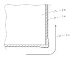
- the semiconductor chip 30 and the substrate 29 are not damaged.
- Resin 34 is reinforced by filling resin 34 in the gap. This process is called underfill (see FIG. 6).
- a liquid resin 34 is applied along the outer periphery of the semiconductor chip 30, the resin 34 is filled in a gap between the semiconductor chip 30 and the substrate 29 using a capillary phenomenon, and then heated in an oven or the like. 34 is cured.
- a fillet portion 35 filled with the liquid resin 34 is formed at the corner portion formed by the side surface of the semiconductor chip 30 and the substrate 29.
- This fillet portion is called a fillet (see FIG. 7). If the fillet 35 is not formed uniformly, air may enter from a small portion of the fillet 35 and cause bubbles to be entrained, or the resin 34 may protrude to the application prohibited area around the application target chip 30, or may be heat-cured. There is a disadvantage that the semiconductor chip 30 may be damaged at the time. Therefore, the fillet 35 needs to be uniformly formed with a constant width (reference numeral 36) and height (reference numeral 37).
- Patent Document 1 As a technique for uniformly forming a fillet, a technique described in Patent Document 1 and a technique described in Patent Document 2 have been proposed (disclosed). That is, in Patent Document 1, in a manufacturing method for manufacturing a semiconductor package having a structure in which a resin is filled between a semiconductor chip and a mounting substrate, the speed of a nozzle for supplying the resin is adjusted to adjust the semiconductor A semiconductor package manufacturing method is disclosed in which the resin supplied from one side of the chip is greater in the central portion of the semiconductor chip than in the end portion of the semiconductor chip.
- a nozzle is moved around a semiconductor chip face-down bonded to a wiring board, an underfill material is continuously supplied from the nozzle, and an underfill material is provided between the wiring board and the semiconductor chip.
- the movement trajectory of the nozzle includes a linear trajectory within a pair of line segments drawn from both ends of the side of the semiconductor chip so as to be perpendicular to the side, and an adjacent linear trajectory.
- a method is disclosed in which a direction change locus that changes direction for connection is continuous, and at least a part of the linear locus moves the nozzle slower than the direction change locus.
- the supply amount adjustment technique disclosed in Patent Document 1 and Patent Document 2 described above is performed by adjusting the moving speed of the nozzle while applying and drawing the liquid resin supplied from the nozzle.
- changing the moving speed of the nozzle during coating drawing has a problem that the load on the driving means increases, and the larger the difference in nozzle moving speed, the more the load is applied and the life of the driving means is shortened.
- the supply amount is adjusted according to the moving speed of the nozzle, there is a problem that the control becomes complicated.
- the change in the nozzle moving speed during coating drawing also causes unnecessary vibrations in the apparatus, and there is a problem that the coating accuracy is deteriorated.
- the present invention eliminates the disturbance of the fillet shape due to the difference in permeability when the bumps are non-uniformly arranged and the speed difference associated with the direction change of the nozzle, and can maintain the fillet shape constant. And to provide a program.
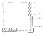
- the cause of the disorder of the fillet shape is also due to the arrangement of the bumps 31 formed on the semiconductor chip 30 in solving the above-described problems.
- the liquid resin 34 is filled in the gap between the semiconductor chip 30 and the substrate 29 by capillary action.
- the degree of penetration of the liquid resin 34 into the gap is influenced by the arrangement density of the bumps 31 existing in the back of the gap in addition to the width of the gap. For example, consider a semiconductor chip 30 as shown in FIG. It is assumed that application is performed along one side of the semiconductor chip 30. In general, the portion 38 where the bumps 31 are arranged densely penetrates the liquid resin 34, and the portion 39 where the bumps 31 are arranged loosely penetrates the liquid resin 34 slowly.
- the inventors have inferred that there is a relationship between the arrangement of the bumps 31 formed on the semiconductor chip 30 and the fillet shape formed by underfilling the semiconductor chip 30, The hypothesis that the problem can be solved by changing the coating amount per unit area was verified.
- adjusting the supply amount from the discharge device is effective for changing the application amount per unit area in the application target region. That is, in order to form the fillet shape uniformly without being affected by the bump arrangement, it has been found that it is important to apply a necessary amount per unit area in the application target region. In addition, it has been found that it is important to supply the necessary amount per unit area in the application target region in order to form the fillet shape uniformly without being affected by the speed change caused by the direction change. It was. In addition, as a means for changing the application amount per unit area in the application target region on the discharge device side, based on the recognition that a discharge device of the type that makes the discharge device fly or drop-like discharge is effective, The present invention has been made with diligence.
- the first invention creates a desired coating pattern, discharges the liquid material from the nozzle while moving the nozzle and the workpiece relative to each other, and places the workpiece placed on the substrate and three or more bumps thereon.
- the liquid material is applied by filling the gap with the liquid material using a capillary phenomenon, and when the bumps are non-uniformly arranged, the supply amount per unit area in the application pattern is set to
- the liquid material application method is characterized in that the area where the degree of integration of the bumps is higher and the area where the bumps are adjacent are set to be larger than the area where the degree of integration is lower and the area where the application is adjacent.
- a second invention is characterized in that, in the first invention, the supply amount of a coating region adjacent to a region having a high degree of bump integration is increased as compared to a coating region adjacent to a region having a low degree of bump integration.
- a third invention is characterized in that, in the first or second invention, the supply amount of a coating region adjacent to a region having a low integration degree of bumps is reduced as compared with a coating region adjacent to a region having a high integration degree of bumps. .
- a desired coating pattern is created, a liquid material is ejected from the nozzle while moving the nozzle and the workpiece relative to each other, and the substrate and the workpiece placed thereon via three or more bumps
- a liquid material application method that uses capillary action to fill the gap, and the number of times that the ejection pulse signal and pause pulse signal are transmitted is defined as the total number of pulses.
- An initial parameter setting step that defines the number of ejection pulse signals necessary to perform and the rest as pause pulse signals, a correction amount calculation step that measures the ejection amount from the ejection device and calculates the ejection amount correction amount, And a discharge amount correction step of adjusting the number of discharge pulse signals and the number of pause pulse signals based on the correction amount calculated in the correction amount calculation step, wherein the discharge amount correction step includes uneven bumps.
- the discharge amount correction step includes uneven bumps.
- a liquid material is discharged from the nozzle while moving the nozzle and the workpiece relative to each other, and a capillary phenomenon is used in a gap between the substrate and the workpiece placed on the substrate via three or more bumps.
- a method of applying a liquid material to be filled with a liquid material the step of creating a coating pattern composed of a plurality of continuous coating areas, and a predetermined number of ejection pulse signals and a number of pause pulse signals in each coating area.
- a discharge cycle assignment step for assigning a plurality of discharge cycles combined in proportion
- a correction amount calculation step for measuring a discharge amount from the discharge device and calculating a correction amount for the discharge amount
- a bump In the correction amount calculating step, the supply amount per unit area of the coating region adjacent to the region having a high degree of bump integration and the coating region adjacent to the coating region adjacent to the region having a low bump integration amount is increased.
- the liquid material application method includes: a discharge amount correction step including a step of adjusting the length of each of the application regions without changing the discharge amount per unit time.
- the sixth invention is characterized in that, in the fourth or fifth invention, the ejection amount is corrected without changing the frequency at which the ejection pulse signal and the pause pulse signal are transmitted.
- the seventh invention creates a desired coating pattern, discharges a liquid material from the nozzle while relatively moving the nozzle and the workpiece, and includes a substrate and a workpiece placed on the substrate via three or more bumps.
- a liquid material application method that fills the gap with a liquid material using capillary action, an initial parameter setting step that defines the interval between unit cycles for performing one discharge, and measures the discharge amount from the discharge device,
- a correction amount calculating step for calculating a correction amount for the discharge amount and, when bumps are arranged unevenly, adjacent to a region having a higher bump integration degree than a coating region adjacent to a region having a lower bump integration degree
- a fee of coating method is provided.
- the coating pattern when the coating pattern is a coating pattern that does not require a change in direction of the nozzle, coating is performed without changing the relative movement speed of the nozzle and the workpiece. It is characterized by performing.
- the coating pattern when the coating pattern is a coating pattern including a coating region that requires a change in direction of a nozzle, the supply amount per unit area in the coating pattern is The liquid material is set so as to be more in the application area where the direction change of the nozzle is not required than in the application area where the direction change of the nozzle is required.
- a tenth invention includes a discharge device including a nozzle, a drive mechanism that relatively moves the discharge device and the workpiece, a detection device that detects the shape of the applied liquid material, and a control unit that controls these operations.
- the liquid material coating apparatus is characterized by causing a control unit to perform the coating method according to any one of the first to ninth inventions.
- the eleventh invention includes a discharge device including a nozzle, a drive mechanism that relatively moves the discharge device and the workpiece, a detection device that detects the shape of the applied liquid material, and a control unit that controls these operations.
- the program causes the control unit to perform the coating method according to any one of the first to ninth inventions.
- the present invention it is possible to eliminate the disturbance of the fillet shape due to the difference in the degree of penetration when the bumps are non-uniformly arranged and the speed difference accompanying the change of direction of the nozzle, and to keep the fillet shape constant. Further, since it is not necessary to change the relative movement speed of the nozzles except for the direction change, it is possible to reduce the load applied to the drive mechanism, thereby suppressing the occurrence of vibrations and improving the accuracy.
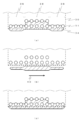
- (B) It is the top view which saw through one part for demonstrating the fillet shape after apply
- the discharge device used in the present embodiment is a jet type discharge device that receives a pulse signal, drives a valve body, and causes the valve body to collide with a valve seat to fly and discharge a liquid material from a nozzle.
- One discharge in this discharge apparatus is performed by receiving one pulse signal.
- coating is performed by transmitting the pulse signal at a preset frequency.
- a procedure for adjusting the coating amount per unit area (or unit length) in the application target region in the ejection device according to the present embodiment will be described (see FIG. 1).
- the present invention can be applied to any type of ejection device that performs flight ejection or droplet ejection, and is not limited to application to a jet type.
- the required amount may be obtained from a theoretical value from a design drawing or the like, or may be obtained by actually applying. Here, since the theoretical value is an ideal value to the last, it is preferable to obtain it by actually performing coating in order to ensure accuracy. Moreover, a required amount may be calculated
- the amount discharged in one discharge and the time required for one discharge are determined by the properties of the liquid material, the shape (diameter, length) of the nozzle, the amount of movement (stroke) of the valve body, etc. It is preferable to measure by actually discharging. In that case, the accuracy can be improved by performing discharge a plurality of times and obtaining the average value.
- the sides to be coated are set in consideration of the arrangement of bumps (connection portions) connecting the workpiece and the substrate, the status of other parts around the workpiece, and the like. For example, in a rectangular workpiece, setting is performed such that application is performed linearly along one side, or application is performed in an L shape along two adjacent sides. This is the coating pattern. When the application pattern is determined, the application length is obtained. From this coating length and the ejection time obtained in the above (1), the moving speed when uniform in all coating patterns is temporarily determined.
- a coating pattern is created in consideration of the coating amount and coating length determined by the workpiece shape.
- “application length” means the total length of relative movement between the nozzle and the workpiece.
- the application pattern is composed of one or more ejection pulses and zero or more pause pulses.
- a pulse signal composed of an ejection pulse and a pause pulse is transmitted at a predetermined frequency.
- the frequency and the number of shots / second are the same.
- the frequency is preferably several tens of hertz or more, and more preferably several hundreds of hertz.
- the frequency is determined from the total length of the coating pattern, the weight or volume of the liquid material 34 required for the desired coating pattern.
- Initial parameter setting (STEP 104) The following parameters are set as initial parameters.
- the predetermined frequency has an optimum frequency range, and if it is outside this range, problems such as not being ejected occur. Therefore, the range for normal ejection is determined in advance by experiments. Although it depends on the characteristics of the liquid material and the discharge amount, for example, it is used at about 100 to 200 hertz. By the way, the frequency range is determined based on the mechanical response performance and the characteristics of the liquid material.
- the discharge amount changes.
- the frequency is out of the optimum frequency range, a problem such as ejection does not occur, and the change characteristic of the discharge amount due to the change in frequency is not linear. Therefore, basically, it is preferable not to change the frequency once set within the same coating pattern.
- the discharge amount can be adjusted by changing the frequency within the range. Specifically, it is as follows. It is assumed that a pulse signal that is one unit cycle with an on-state time of 3 msec and an off-state time of 4 msec is optimal for achieving a desired discharge amount. The frequency of this cycle is about 142 hertz.
- the on-state time is fixed, and the off-state time is varied.
- the frequency is about 166 hertz, and if it is 2 msec, the frequency is 200 hertz, so the limit is up to 2 msec.
- the off-state time is 5 msec
- the frequency is 125 hertz, about 111 hertz at 6 msec, and 100 hertz at 7 msec, so the limit is up to 7 msec.
- the limit range of the off-state time is determined, an experiment is performed in advance for each of the plurality of on / off time settings, and the relationship with the discharge amount is obtained and stored in the control unit. Then, at the time of adjustment described later, a setting suitable for adjustment is selected from these.
- the on / off time is an integer, but it goes without saying that the on / off time can be a real number (decimal number) in order to obtain more detailed setting values.
- the value closest to the boundary of the frequency range described above may be changed to a range where troubles such as non-injection occur due to the influence of changes in the characteristics of the liquid material and ambient temperature. It is preferable to set the on / off time, that is, the frequency with a margin.
- the number of ejection pulses and the number of pause pulses constituting the coating pattern are set.
- the controller stores in advance a setting table that prescribes combinations of the number of ejection pulses and the number of pause pulses.
- Table 1 is an example of a setting table stored in the control unit.
- setting example A shows a setting example of the discharge amount when the total number of pulses is 100
- setting example B shows a setting example of the discharge amount when the total number of pulses is 111
- setting example C shows the total number of pulses.
- An example of setting the discharge amount when the number is 125 is shown.
- the number of ejection pulses corresponds to the ejection amount, and the ejection amount can be adjusted by increasing or decreasing the number of pause pulses in the total number of pulses.
- Setting example A prescribes a setting example for changing the discharge amount based on a combination in which no pause pulse is set for one ejection pulse (zero pause pulse) when the number of ejection pulses is 100.
- Setting example B is a setting example for changing the discharge amount based on the combination of setting one pause pulse (11 pause pulses) for nine discharge pulses when the number of discharge pulses is 100. Is stipulated.
- Setting example C is a setting example for changing the discharge amount based on a combination of setting one pause pulse (25 pause pulses) for four discharge pulses when the number of discharge pulses is 100. Is stipulated. When increasing the number of pause pulses, or when increasing or decreasing the number of pause pulses in the discharge amount correction described later, it is preferable to set the initial parameters so that the timing of the pause pulses is equally spaced. In the underfill process, when the number of pause pulses is increased to two or three times, the number of ejection pulses relative to the number of pause pulses is reduced rather than increasing the gap (non-coating region) by continuing the number of pause pulses. Therefore, it is preferable to reduce the gap (non-application region) from the viewpoint of preventing entrainment of bubbles.
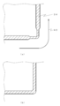
- parameters are adjusted so that the line width is widened.
- the unit area at the corner portion is such that the widened portion has the same width as the straight portion.
- Adjust the parameters to reduce the amount of supply per unit That is, as an application pattern, an actual application in which the nozzle movement speed is reduced by creating an application pattern with a small supply amount per unit area at the corner as shown in FIG. A fillet having a line width equivalent to that of the straight portion as shown in b) is formed. Specific parameter types to be adjusted will be described later.
- the parameters are adjusted so that the fillet width is widened.
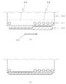
- the line width is narrow in a dense bump area (high integration density)
- this narrow area is equivalent to a sparse bump area (low integration density area).
- the parameters are adjusted so as to increase the supply amount per unit area in a portion where the bumps are dense so that the width becomes.
- the parameter may be adjusted to reduce the supply amount per unit area in a portion where the bumps are sparse.
- FIG. 12A is an application pattern in which the supply amount per unit area is large at a dense bump location and the supply amount per unit area is small at a location where bumps are sparse.
- a fillet having a certain width as shown in FIG. 12B is formed.
- the fillet height may be imaged and measured by an imaging device, and parameters relating to ejection may be adjusted based on the measurement result.
- the fillet height may be imaged and measured by an imaging device, and parameters relating to ejection may be adjusted based on the measurement result.
- the fillet width (coating line width) differs as shown in FIG. Arise. Therefore, per unit area in a dense bump area so that the fillet width (applied line width) in a dense bump area is the same as the fillet width (applied line width) in a sparse bump area.
- the parameter is adjusted in order to increase the supply amount or reduce the supply amount per unit area at a portion where the bumps are sparse. That is, by creating a coating pattern as shown in FIG. 13B, a fillet having a constant width as shown in FIG. 13C can be obtained. Specific parameter types to be adjusted will be described later.
- (Iii) Types of parameters relating to ejection The parameters relating to ejection that are changed when performing the adjustment described above are listed below.
- (Iii-1) Discharge frequency (unit cycle) In order to change the coating amount per unit area in the discharge that repeats the unit cycle at the predetermined frequency, the interval between the unit cycles is adjusted based on the values set in (4) and (i) above. Specifically, when the unit cycle interval is narrowed, the coating amount increases, and when the unit cycle interval is widened, the coating amount decreases.
- the relationship between the unit cycle interval and the discharge amount is obtained by experiments in advance and stored in the control unit or the like in the form of a setting table or calculation formula.
- the ejection pulse signal which is a signal for performing ejection and the signal which does not perform ejection, as set in the above (4) (ii).
- the table that defines the number of times to send the pause pulse signal as the total number of pulses, the number of ejection pulse signals necessary to achieve the coating amount of the total number of pulses, and the rest as the pause pulse signal The coating amount is changed by changing the number of ejection pulse signals and pause pulse signals.
- the application amount decreases, and when the pause pulse signal is decreased, the application amount increases.
- the relationship between the number of ejection pulses and the number of pause pulses and the ejection amount is obtained by experiments in advance and stored in the control unit or the like in the form of a setting table or a calculation formula. Note that, by changing the number of pulses, the application amount can be changed without changing the application length.
- the application amount per unit area can also be changed by adjusting the discharge amount change factor of the discharge device. For example, it is performed by adjusting a discharge amount changing factor of the following discharge device. 1) “Pressure” applied to the storage container, 2) “Stroke”, which is the travel distance in one operation of the valve body, 3) “Temperature” of the heater that warms the vicinity of the nozzle, 4) “Nozzle diameter” of the nozzle that discharges liquid material
- the magnitude of each of the factors corresponds to the magnitude of the discharge amount of the liquid material.
- the optimum parameter (iii-1) to (iii-3) is selected based on the result of measuring the line width and fillet width after coating on a bare substrate or workpiece. To do. Further, the adjustment may be performed by combining a plurality of parameters among (iii-1) to (iii-3). For example, based on the adjustment of the parameter (iii-2) above, the parameter (iii-1) or (iii-3) is supplementarily used when the limit of the adjustment range is reached or when fine adjustment is performed. A method of performing adjustment can be taken.
- the coating amount per unit area in the coating target region can be changed, so that the fillet shape is not disturbed by the influence of the bump arrangement or the speed change due to the direction change, and the fillet The shape can be kept constant. Further, since the moving speed is not changed except for the direction change, the load applied to the drive mechanism can be reduced, thereby suppressing the occurrence of vibration, improving the accuracy, and extending the life.
- the discharge device 1 includes a piston 2 that is a valve body inscribed in a vertically movable manner, a storage container 3 that is pressurized by a compressed gas that is regulated through a control unit 11, A nozzle 4 communicating with the container 3 is provided. Moreover, the switching valve 6 which supplies / exhaustes the working gas for moving the piston 2 upward through the control part 11, and the spring 7 which moves the piston 2 below are provided. A stroke adjusting member 8 for adjusting the moving amount of the piston 2 is provided on the upper portion of the spring 7. Further, a heater 9 for warming the nozzle 4 and the liquid material 34 in the nozzle 4 is provided in the vicinity of the nozzle 4.
- a temperature sensor 10 is provided on the opposite side of the heater 9 and is used when control is performed to keep the nozzle 4 and the liquid material 34 in the nozzle 4 at a predetermined temperature.
- the liquid material 34 filled in the storage container 3 is ejected from the nozzle 4 in the form of droplets by operating the switching valve 6 according to the pulse signal transmitted from the control unit 11 and moving the piston 2 up and down.
- the liquid material 34 discharged from the nozzle 4 is applied in a dotted manner to the substrate 29, the weighing instrument 22, and the like positioned under the nozzle 4.
- the discharge device 1 reciprocates the piston 2 once in response to a single pulse signal, and discharges a drop of the liquid material 34 from the nozzle 4. That is, one unit cycle corresponds to one shot.
- the pulse signal is given as shown in FIG. 3, for example.
- the pulse signal is turned on (left side of reference numeral 14)
- gas is supplied by the operation of the switching valve 6, the piston 2 is raised, and the nozzle inlet 5 is opened.
- the pulse signal is turned off (right side of reference numeral 14)
- the gas is exhausted by the operation of the switching valve 6, the piston 2 is lowered by the repulsive force of the spring 7, and the nozzle inlet 5 is closed.
- the rising of the piston 2 (opening of the nozzle inlet 5) and the lowering of the piston 2 (closing of the nozzle inlet 5) are set as one unit cycle, and one drop of the liquid material 34 is discharged by the operation of one unit cycle.
- the pulse signal is OFF (reference numeral 15)
- the piston 2 is not operated and the nozzle inlet 5 is closed by one unit cycle.
- the on-state time (rise time) and off-state time (fall time) in one unit cycle may be adjusted, or the movement amount of the piston 2 may be adjusted using the stroke adjusting member 8. Also good.
- control unit 11 When performing application along the side of the workpiece 30, the control unit 11 transmits a pulse signal at a preset frequency to the ejection device 1 while moving the nozzle 4 simultaneously with the start of application, and continuously liquid material. 34 is discharged.
- the liquid material 34 discharged along the side of the work 30 is filled in the gap between the work 30 and the substrate 29 by capillary action.
- the coating apparatus 16 of the present embodiment includes a discharge device 1, an XYZ drive mechanism 17, a transport mechanism 18, a coating stage 19, an adjustment substrate 20, and an adjustment stage on which the adjustment substrate 20 is placed. 21, a weighing instrument 22, a detection device (touch sensor 23, laser displacement meter 24 and camera 25), and control unit 11.
- the discharge device 1 is the jet-type discharge device described above, and receives the pulse signal from the control unit 11 and discharges the liquid material 34.
- the XYZ drive mechanism 17 is provided with a discharge device 1 and a laser displacement meter 24 and a camera 25 which are a part of a detection device described later.
- the discharge device 1, the laser displacement meter 24 and the camera 25 are moved in the XYZ directions indicated by reference numeral 26. Can be moved. That is, based on the application pattern set in the control unit 11, the ejection device 1 is moved above the substrate 29, the weighing device 22, or a touch sensor 23 that is a part of a detection device described later that is fixed at another position.
- the discharge device 1, the laser displacement meter 24, and the camera 25 can be moved to an adjustment stage 21 on which an adjustment substrate 20 (described later) is placed.
- the transport mechanism 18 carries the substrate 29 on which the work 30 before the coating operation is placed from the direction indicated by reference numeral 27 outside the device, and transports the substrate 29 close to the discharge device 1 that performs the coating operation. And the board
- work is carried out in the direction shown with the code
- the coating stage 19 is installed between the conveyance mechanisms 18 in the substantially center of the conveyance mechanism 18. When performing the coating operation, it raises and fixes the substrate 29. When transporting the substrate 29, it is lowered so as not to hinder the transport.
- the adjustment stage 21 is installed in the vicinity of the transport mechanism 18.
- a substrate (generally referred to as an adjustment substrate 20) on which an elementary substrate or a dummy workpiece is mounted is placed on the substrate, and coating is performed in accordance with the adjustment operation of the supply amount of the liquid material.
- the weighing device 22 is for measuring the weight of the liquid material 34 discharged from the discharge device 1, and is installed in the vicinity of the transport mechanism 18.
- the measurement result obtained by the weighing instrument 22 is transmitted to the control unit 11.
- the detection device includes a touch sensor 23 that is a sensor that detects the height position of the nozzle 4, a laser displacement meter 24 that is a sensor that detects the height position of the substrate 29, and a camera 25 that detects the position of the workpiece 30.
- the laser displacement meter 24 and the camera 25 are installed in the XYZ drive mechanism 17 together with the discharge device 1 and are movable in the XYZ directions.
- the touch sensor 23 is fixed to the adjustment stage 21.
- the control unit 11 includes an overall control unit that controls the operation of the entire device 16 and a discharge control unit that controls the operation of the discharge device 1.
- the number of ejection pulses and the number of pause pulses are set as initial parameters (see Table 1 above).
- the displacement of the application position is calibrated (STEP 502).
- linear coating is performed on a bare substrate, and then the camera is moved by a preset nozzle-camera distance to image the applied liquid material.
- it is measured by measuring how much the imaged liquid material is deviated from the center of the camera and adjusting the deviation.
- settings relating to image recognition of the application work are performed (STEP 503). This is a reference when performing alignment (alignment with respect to distortion or bending of a workpiece or a substrate).
- a series of operations for adjusting the supply amount from the discharge device described in the above embodiment is performed (STEP 504). That is, as described in the embodiment for carrying out the invention, the supply amount of the liquid material is adjusted by using parameters relating to ejection alone or in combination.
- the location and number of inspections such as the presence / absence and width of the fillet are set (STEP 505).
- values that are criteria for pass / fail judgment such as target values and allowable values are also set.
- a reference value is set when the coating amount is corrected during the subsequent coating operation (STEP 506).
- the weight when discharging for a predetermined time or the number of shots to the weighing device provided in the coating apparatus is measured and stored in the control unit.
- application is performed on the mounting substrate to be actually applied, and final confirmation is performed (STEP 507). If there is no defect after the final confirmation, the present coating operation is started (STEP 508).
- the substrate is first carried in, transported to the vicinity of the discharge device, and then fixed to the coating stage (STEP 509). Then, image recognition by a camera is performed on the substrate on the application stage, and alignment is performed to perform alignment. After the alignment is completed, application is performed (STEP 510).
- the substrate that has been coated is carried out of the coating apparatus (STEP 511). It is determined whether or not the number of applied substrates has reached a preset correction cycle (for example, the number of workpieces or the number of substrates) at the time when the coated substrate is unloaded (STEP 512). If the correction period has been reached, the process proceeds to the correction process described below. If not, the process proceeds to STEP 515.
- a preset correction cycle for example, the number of workpieces or the number of substrates
- the correction process includes positional deviation correction (STEP 513) and application amount correction (STEP 514).
- positional deviation correction the same operation as in STEP 502 is performed to adjust the amount of deviation.
- application amount correction first, discharge is performed for a predetermined time or the number of shots to the weighing device, and the weight is measured. Then, the measured weight is compared with the reference weight measured in STEP 506, and if the allowable value is exceeded, the discharge device and the coating device are adjusted to correct the reference weight.
- a correction method for example, there are the following two methods.
- (A) Correction method in point-like application The number of times of transmitting the ejection pulse signal and the pause pulse signal is defined as the total number of pulses, and the number of ejection pulse signals necessary to achieve the coating amount is defined out of the total number of pulses. Then, the rest is defined as a pause pulse signal, and the supply amount of the liquid material is corrected by adjusting the number of ejection pulse signals and the number of pause pulse signals based on the correction amount calculated in the correction cycle.
- a setting table that prescribes a setting that takes into account the increase or decrease of the discharge amount is stored in the control unit in advance, and correction is performed by selecting a combination of the number of discharge pulses and pause pulses from the setting table. It is preferred to do so.
- (B) Correction method in linear coating A coating pattern comprising a plurality of continuous coating regions is created, and a discharge cycle (unit cycle) in which the number of discharge pulses and the number of pause pulses are combined in each coating region at a predetermined ratio. And a number of discharge pulses and pause pulses included in the application pattern are adjusted based on the correction amount calculated in the correction cycle, and / or at least one application region and the application region are continuous.
- the supply amount of the liquid material is corrected by adjusting the length of the other one or two application regions without changing the discharge amount per unit time in each application region. It is preferable to correct the ejection amount without changing the frequency at which the ejection pulse and the pause pulse are transmitted.
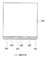
- FIG. 14 is a diagram showing an example of an application pattern by dot application.
- the application region 141 corresponds to the ejection pulse.
- the ejection amount in the application region 141 is controlled by setting an ejection pulse, whereby the length of the application region 141 is expanded and contracted.
- region 142 expands and contracts by setting a pause pulse.
- a method for calculating the correction amount the weight when discharging for a certain period of time is measured, the method for calculating the correction amount based on the difference from the appropriate weight, and the discharge time required to reach the appropriate weight are measured.
- any method may be adopted.
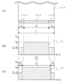
- FIG. 15 is a diagram showing an example of a coating pattern in which a coating region is divided into a plurality of portions in a linear coating and a coating amount is changed for each coating region.
- a first discharge cycle in which the discharge pulse and the pause pulse are combined at a first ratio
- a second discharge cycle in which the discharge pulse and the pause pulse are combined in a second ratio are created.
- One application region 151 that performs discharge corresponding to the discharge cycle of the first and the second application regions 152 and 152 that perform discharge corresponding to the second discharge cycle are connected to both ends thereof to form one application pattern. It is composed.
- the application regions 152 and 152 are associated with the second discharge cycle, but the present invention is not limited to this.
- One of the application regions 152 is associated with the second discharge cycle and the other is the third discharge cycle. It is possible to correspond to the discharge cycle.
- the number of application areas allocated to one discharge cycle can be set to an arbitrary number.
- a discharge pulse and a pause pulse are assigned to each application region. For example, in FIG. 15, if it is desired that the discharge amount in the first application region 151 is larger than that in the second application region 152, the first application region 151 has four discharge pulses from the setting example A in Table 1. A combination of one pause pulse (80% ejection) is selected and set in the second application region 152 by one pause pulse combination (75% ejection) for three ejection pulses. In the correction, the number of ejection pulses and pause pulses is adjusted in the same manner as described in (a) above. Adjustment of the length of each application area means adjusting the length of a plurality of application areas having different application amounts per unit length constituting the application pattern. In the case of FIG. 15, the application amount increases when the first application region 151 becomes longer, and the application amount decreases when the first application region 151 becomes shorter. At this time, it is preferable to adjust the length of each application region without changing the overall length of the application pattern.
- the area of the convex portion S1 surrounded by the diagonal lines corresponds to the coating amount before correction.
- the area of the convex portion S0 surrounded by the oblique lines in the graph shown in FIG. 15C corresponds to the corrected application amount.
- the application amount can be increased by increasing the length of X1 and shortening the length of X2. It should be noted that even when a digital correction by adjusting the number of pulses causes a shift in the correction amount, it is possible to avoid a shift in the correction amount by adjusting the length of the analog application region.
- the present invention can be applied to a type in which the discharged liquid material is separated from the nozzle before contacting the application target.
- a jet type that causes the valve body to collide with the valve seat, and ejects the liquid material from the nozzle tip.
- a plunger jet type that moves the plunger type plunger, then stops suddenly, and also ejects and ejects from the nozzle tip.
- An ink jet type or an on-demand type is available.
- the present invention can be used in an underfill process of semiconductor packaging.
Landscapes
- Engineering & Computer Science (AREA)
- Manufacturing & Machinery (AREA)
- Computer Hardware Design (AREA)
- Microelectronics & Electronic Packaging (AREA)
- Power Engineering (AREA)
- Physics & Mathematics (AREA)
- Condensed Matter Physics & Semiconductors (AREA)
- General Physics & Mathematics (AREA)
- Coating Apparatus (AREA)
- Application Of Or Painting With Fluid Materials (AREA)
- Spray Control Apparatus (AREA)
- Encapsulation Of And Coatings For Semiconductor Or Solid State Devices (AREA)
Priority Applications (5)
| Application Number | Priority Date | Filing Date | Title |
|---|---|---|---|
| KR1020127006243A KR101700255B1 (ko) | 2009-08-11 | 2010-08-06 | 액체 재료의 도포 방법, 도포 장치 및 프로그램을 기억한 기억 매체 |
| US13/389,895 US8703601B2 (en) | 2009-08-11 | 2010-08-06 | Method for applying liquid material, application device and program |
| EP10808171.2A EP2466630B1 (en) | 2009-08-11 | 2010-08-06 | Method for applying liquid material, application device and programme |
| HK12112373.8A HK1171573B (en) | 2009-08-11 | 2010-08-06 | Method for applying liquid material and application device |
| CN201080045483.7A CN102714165B (zh) | 2009-08-11 | 2010-08-06 | 液体材料的涂布方法以及涂布装置 |
Applications Claiming Priority (2)
| Application Number | Priority Date | Filing Date | Title |
|---|---|---|---|
| JP2009-186349 | 2009-08-11 | ||
| JP2009186349A JP5783670B2 (ja) | 2009-08-11 | 2009-08-11 | 液体材料の塗布方法、塗布装置およびプログラム |
Publications (1)
| Publication Number | Publication Date |
|---|---|
| WO2011018988A1 true WO2011018988A1 (ja) | 2011-02-17 |
Family
ID=43586165
Family Applications (1)
| Application Number | Title | Priority Date | Filing Date |
|---|---|---|---|
| PCT/JP2010/063346 Ceased WO2011018988A1 (ja) | 2009-08-11 | 2010-08-06 | 液体材料の塗布方法、塗布装置およびプログラム |
Country Status (7)
| Country | Link |
|---|---|
| US (1) | US8703601B2 (enExample) |
| EP (1) | EP2466630B1 (enExample) |
| JP (1) | JP5783670B2 (enExample) |
| KR (1) | KR101700255B1 (enExample) |
| CN (1) | CN102714165B (enExample) |
| TW (1) | TWI497613B (enExample) |
| WO (1) | WO2011018988A1 (enExample) |
Cited By (2)
| Publication number | Priority date | Publication date | Assignee | Title |
|---|---|---|---|---|
| JP2018199130A (ja) * | 2018-06-04 | 2018-12-20 | 武蔵エンジニアリング株式会社 | 液体材料塗布装置および液体材料塗布方法 |
| TWI665021B (zh) * | 2017-05-25 | 2019-07-11 | 日商武藏工業股份有限公司 | Liquid material coating device and liquid material coating method |
Families Citing this family (11)
| Publication number | Priority date | Publication date | Assignee | Title |
|---|---|---|---|---|
| JP5280702B2 (ja) * | 2008-02-18 | 2013-09-04 | 武蔵エンジニアリング株式会社 | 液体材料の塗布方法、その装置およびそのプログラム |
| JP5632838B2 (ja) * | 2009-06-15 | 2014-11-26 | 武蔵エンジニアリング株式会社 | 液体材料の塗布方法、その装置およびそのプログラム |
| JP6452147B2 (ja) * | 2015-01-19 | 2019-01-16 | 武蔵エンジニアリング株式会社 | 液体材料吐出装置 |
| JP2016131947A (ja) * | 2015-01-21 | 2016-07-25 | 三菱電機株式会社 | 液剤塗布方法および電子装置の製造方法ならびに液剤塗布装置 |
| US9653325B2 (en) * | 2015-02-17 | 2017-05-16 | Powertech Technology Inc. | Underfill process and processing machine thereof |
| JP6684397B2 (ja) * | 2015-04-02 | 2020-04-22 | エムテックスマート株式会社 | 流体の噴出方法および流体の成膜方法 |
| CN106094271A (zh) * | 2016-06-22 | 2016-11-09 | 深圳市华星光电技术有限公司 | 一种显示面板切割方法 |
| JP6778426B2 (ja) * | 2016-09-20 | 2020-11-04 | 武蔵エンジニアリング株式会社 | 液体材料吐出装置 |
| JP6991475B2 (ja) * | 2017-05-24 | 2022-01-12 | 協立化学産業株式会社 | 加工対象物切断方法 |
| CN108906508B (zh) * | 2018-08-06 | 2020-11-27 | Oppo(重庆)智能科技有限公司 | 胶量控制方法及胶量控制装置 |
| JP7426198B2 (ja) * | 2019-04-17 | 2024-02-01 | 株式会社ジャノメ | 塗布装置 |
Citations (3)
| Publication number | Priority date | Publication date | Assignee | Title |
|---|---|---|---|---|
| JPH1050769A (ja) | 1996-07-30 | 1998-02-20 | Toshiba Corp | 半導体パッケージの製造装置および製造方法 |
| JP2007194403A (ja) * | 2006-01-19 | 2007-08-02 | Sony Corp | 電子デバイスの製造装置及び電子デバイスの製造方法、並びに、アンダーフィル材充填状態の検査装置及びアンダーフィル材充填状態の検査方法 |
| JP2008071883A (ja) | 2006-09-13 | 2008-03-27 | Seiko Epson Corp | 半導体装置の製造方法 |
Family Cites Families (10)
| Publication number | Priority date | Publication date | Assignee | Title |
|---|---|---|---|---|
| JP2571024B2 (ja) | 1994-09-28 | 1997-01-16 | 日本電気株式会社 | マルチチップモジュール |
| US6066509A (en) | 1998-03-12 | 2000-05-23 | Micron Technology, Inc. | Method and apparatus for underfill of bumped or raised die |
| JP3431406B2 (ja) * | 1996-07-30 | 2003-07-28 | 株式会社東芝 | 半導体パッケージ装置 |
| US7015592B2 (en) * | 2004-03-19 | 2006-03-21 | Intel Corporation | Marking on underfill |
| WO2006118089A1 (ja) * | 2005-04-28 | 2006-11-09 | Shibaura Mechatronics Corporation | 溶液の塗布装置及び塗布方法 |
| JP2007173621A (ja) * | 2005-12-22 | 2007-07-05 | Sharp Corp | 基板に対する液膜材料の塗布方法 |
| JP4871093B2 (ja) | 2006-11-01 | 2012-02-08 | 武蔵エンジニアリング株式会社 | 液体材料の充填方法、装置およびプログラム |
| JP4868515B2 (ja) * | 2006-11-01 | 2012-02-01 | 武蔵エンジニアリング株式会社 | 液体材料の充填方法、装置およびプログラム |
| JP5019900B2 (ja) * | 2007-02-08 | 2012-09-05 | 武蔵エンジニアリング株式会社 | 液体材料の充填方法、装置およびプログラム |
| JP4962413B2 (ja) * | 2008-05-28 | 2012-06-27 | セイコーエプソン株式会社 | 液状体吐出装置、及び液状体吐出方法 |
-
2009
- 2009-08-11 JP JP2009186349A patent/JP5783670B2/ja active Active
-
2010
- 2010-08-06 CN CN201080045483.7A patent/CN102714165B/zh active Active
- 2010-08-06 EP EP10808171.2A patent/EP2466630B1/en active Active
- 2010-08-06 US US13/389,895 patent/US8703601B2/en active Active
- 2010-08-06 WO PCT/JP2010/063346 patent/WO2011018988A1/ja not_active Ceased
- 2010-08-06 KR KR1020127006243A patent/KR101700255B1/ko active Active
- 2010-08-10 TW TW099126593A patent/TWI497613B/zh active
Patent Citations (3)
| Publication number | Priority date | Publication date | Assignee | Title |
|---|---|---|---|---|
| JPH1050769A (ja) | 1996-07-30 | 1998-02-20 | Toshiba Corp | 半導体パッケージの製造装置および製造方法 |
| JP2007194403A (ja) * | 2006-01-19 | 2007-08-02 | Sony Corp | 電子デバイスの製造装置及び電子デバイスの製造方法、並びに、アンダーフィル材充填状態の検査装置及びアンダーフィル材充填状態の検査方法 |
| JP2008071883A (ja) | 2006-09-13 | 2008-03-27 | Seiko Epson Corp | 半導体装置の製造方法 |
Cited By (5)
| Publication number | Priority date | Publication date | Assignee | Title |
|---|---|---|---|---|
| TWI665021B (zh) * | 2017-05-25 | 2019-07-11 | 日商武藏工業股份有限公司 | Liquid material coating device and liquid material coating method |
| US10786827B2 (en) | 2017-05-25 | 2020-09-29 | Musashi Engineering, Inc. | Liquid material application apparatus and liquid material application method |
| US11396028B2 (en) | 2017-05-25 | 2022-07-26 | Musashi Engineering, Inc. | Liquid material application apparatus and liquid material application method |
| US12162027B2 (en) | 2017-05-25 | 2024-12-10 | Musashi Engineering, Inc. | Liquid material application apparatus and liquid material application method |
| JP2018199130A (ja) * | 2018-06-04 | 2018-12-20 | 武蔵エンジニアリング株式会社 | 液体材料塗布装置および液体材料塗布方法 |
Also Published As
| Publication number | Publication date |
|---|---|
| EP2466630A1 (en) | 2012-06-20 |
| US8703601B2 (en) | 2014-04-22 |
| HK1171573A1 (en) | 2013-03-28 |
| CN102714165A (zh) | 2012-10-03 |
| JP5783670B2 (ja) | 2015-09-24 |
| TW201119752A (en) | 2011-06-16 |
| TWI497613B (zh) | 2015-08-21 |
| EP2466630A4 (en) | 2014-02-26 |
| JP2011036800A (ja) | 2011-02-24 |
| CN102714165B (zh) | 2015-04-15 |
| KR20120054629A (ko) | 2012-05-30 |
| KR101700255B1 (ko) | 2017-02-13 |
| EP2466630B1 (en) | 2019-10-02 |
| US20120313276A1 (en) | 2012-12-13 |
Similar Documents
| Publication | Publication Date | Title |
|---|---|---|
| JP5783670B2 (ja) | 液体材料の塗布方法、塗布装置およびプログラム | |
| CN103391820B (zh) | 液体材料的涂布方法及涂布装置 | |
| JP5632838B2 (ja) | 液体材料の塗布方法、その装置およびそのプログラム | |
| JP2009190012A (ja) | 液体材料の塗布方法、その装置およびそのプログラム | |
| TWI433242B (zh) | 液體材料之填充方法、裝置及程式之媒體 | |
| TWI404575B (zh) | A method for filling a liquid material, a device, and a recording medium on which a program is recorded | |
| TWI404577B (zh) | A method for filling a liquid material, a device, and a recording medium on which a program is recorded | |
| HK1171573B (en) | Method for applying liquid material and application device | |
| HK1174304B (en) | Method for applying liquid material | |
| HK1174304A (en) | Method for applying liquid material | |
| HK1134799B (en) | Method and apparatus for filling liquid material | |
| HK1131363B (en) | Method and apparatus for filling liquid material | |
| HK1189193B (en) | Application method of liquid material and application device |
Legal Events
| Date | Code | Title | Description |
|---|---|---|---|
| WWE | Wipo information: entry into national phase |
Ref document number: 201080045483.7 Country of ref document: CN |
|
| 121 | Ep: the epo has been informed by wipo that ep was designated in this application |
Ref document number: 10808171 Country of ref document: EP Kind code of ref document: A1 |
|
| NENP | Non-entry into the national phase |
Ref country code: DE |
|
| WWE | Wipo information: entry into national phase |
Ref document number: 2010808171 Country of ref document: EP |
|
| ENP | Entry into the national phase |
Ref document number: 20127006243 Country of ref document: KR Kind code of ref document: A |
|
| WWE | Wipo information: entry into national phase |
Ref document number: 13389895 Country of ref document: US |