WO2011004602A1 - エピタキシャルウェーハおよびその製造方法 - Google Patents
エピタキシャルウェーハおよびその製造方法 Download PDFInfo
- Publication number
- WO2011004602A1 WO2011004602A1 PCT/JP2010/004446 JP2010004446W WO2011004602A1 WO 2011004602 A1 WO2011004602 A1 WO 2011004602A1 JP 2010004446 W JP2010004446 W JP 2010004446W WO 2011004602 A1 WO2011004602 A1 WO 2011004602A1
- Authority
- WO
- WIPO (PCT)
- Prior art keywords
- epitaxial
- wafer
- epitaxial wafer
- epitaxial growth
- dichlorosilane
- Prior art date
- Legal status (The legal status is an assumption and is not a legal conclusion. Google has not performed a legal analysis and makes no representation as to the accuracy of the status listed.)
- Ceased
Links
Images


Classifications
-
- H—ELECTRICITY
- H10—SEMICONDUCTOR DEVICES; ELECTRIC SOLID-STATE DEVICES NOT OTHERWISE PROVIDED FOR
- H10P—GENERIC PROCESSES OR APPARATUS FOR THE MANUFACTURE OR TREATMENT OF DEVICES COVERED BY CLASS H10
- H10P14/00—Formation of materials, e.g. in the shape of layers or pillars
- H10P14/20—Formation of materials, e.g. in the shape of layers or pillars of semiconductor materials
- H10P14/29—Formation of materials, e.g. in the shape of layers or pillars of semiconductor materials characterised by the substrates
- H10P14/2901—Materials
- H10P14/2902—Materials being Group IVA materials
- H10P14/2905—Silicon, silicon germanium or germanium
-
- C—CHEMISTRY; METALLURGY
- C23—COATING METALLIC MATERIAL; COATING MATERIAL WITH METALLIC MATERIAL; CHEMICAL SURFACE TREATMENT; DIFFUSION TREATMENT OF METALLIC MATERIAL; COATING BY VACUUM EVAPORATION, BY SPUTTERING, BY ION IMPLANTATION OR BY CHEMICAL VAPOUR DEPOSITION, IN GENERAL; INHIBITING CORROSION OF METALLIC MATERIAL OR INCRUSTATION IN GENERAL
- C23C—COATING METALLIC MATERIAL; COATING MATERIAL WITH METALLIC MATERIAL; SURFACE TREATMENT OF METALLIC MATERIAL BY DIFFUSION INTO THE SURFACE, BY CHEMICAL CONVERSION OR SUBSTITUTION; COATING BY VACUUM EVAPORATION, BY SPUTTERING, BY ION IMPLANTATION OR BY CHEMICAL VAPOUR DEPOSITION, IN GENERAL
- C23C16/00—Chemical coating by decomposition of gaseous compounds, without leaving reaction products of surface material in the coating, i.e. chemical vapour deposition [CVD] processes
- C23C16/22—Chemical coating by decomposition of gaseous compounds, without leaving reaction products of surface material in the coating, i.e. chemical vapour deposition [CVD] processes characterised by the deposition of inorganic material, other than metallic material
- C23C16/24—Deposition of silicon only
-
- C—CHEMISTRY; METALLURGY
- C30—CRYSTAL GROWTH
- C30B—SINGLE-CRYSTAL GROWTH; UNIDIRECTIONAL SOLIDIFICATION OF EUTECTIC MATERIAL OR UNIDIRECTIONAL DEMIXING OF EUTECTOID MATERIAL; REFINING BY ZONE-MELTING OF MATERIAL; PRODUCTION OF A HOMOGENEOUS POLYCRYSTALLINE MATERIAL WITH DEFINED STRUCTURE; SINGLE CRYSTALS OR HOMOGENEOUS POLYCRYSTALLINE MATERIAL WITH DEFINED STRUCTURE; AFTER-TREATMENT OF SINGLE CRYSTALS OR A HOMOGENEOUS POLYCRYSTALLINE MATERIAL WITH DEFINED STRUCTURE; APPARATUS THEREFOR
- C30B25/00—Single-crystal growth by chemical reaction of reactive gases, e.g. chemical vapour-deposition growth
- C30B25/02—Epitaxial-layer growth
-
- C—CHEMISTRY; METALLURGY
- C30—CRYSTAL GROWTH
- C30B—SINGLE-CRYSTAL GROWTH; UNIDIRECTIONAL SOLIDIFICATION OF EUTECTIC MATERIAL OR UNIDIRECTIONAL DEMIXING OF EUTECTOID MATERIAL; REFINING BY ZONE-MELTING OF MATERIAL; PRODUCTION OF A HOMOGENEOUS POLYCRYSTALLINE MATERIAL WITH DEFINED STRUCTURE; SINGLE CRYSTALS OR HOMOGENEOUS POLYCRYSTALLINE MATERIAL WITH DEFINED STRUCTURE; AFTER-TREATMENT OF SINGLE CRYSTALS OR A HOMOGENEOUS POLYCRYSTALLINE MATERIAL WITH DEFINED STRUCTURE; APPARATUS THEREFOR
- C30B25/00—Single-crystal growth by chemical reaction of reactive gases, e.g. chemical vapour-deposition growth
- C30B25/02—Epitaxial-layer growth
- C30B25/18—Epitaxial-layer growth characterised by the substrate
- C30B25/20—Epitaxial-layer growth characterised by the substrate the substrate being of the same materials as the epitaxial layer
-
- C—CHEMISTRY; METALLURGY
- C30—CRYSTAL GROWTH
- C30B—SINGLE-CRYSTAL GROWTH; UNIDIRECTIONAL SOLIDIFICATION OF EUTECTIC MATERIAL OR UNIDIRECTIONAL DEMIXING OF EUTECTOID MATERIAL; REFINING BY ZONE-MELTING OF MATERIAL; PRODUCTION OF A HOMOGENEOUS POLYCRYSTALLINE MATERIAL WITH DEFINED STRUCTURE; SINGLE CRYSTALS OR HOMOGENEOUS POLYCRYSTALLINE MATERIAL WITH DEFINED STRUCTURE; AFTER-TREATMENT OF SINGLE CRYSTALS OR A HOMOGENEOUS POLYCRYSTALLINE MATERIAL WITH DEFINED STRUCTURE; APPARATUS THEREFOR
- C30B29/00—Single crystals or homogeneous polycrystalline material with defined structure characterised by the material or by their shape
- C30B29/02—Elements
- C30B29/06—Silicon
-
- H—ELECTRICITY
- H10—SEMICONDUCTOR DEVICES; ELECTRIC SOLID-STATE DEVICES NOT OTHERWISE PROVIDED FOR
- H10P—GENERIC PROCESSES OR APPARATUS FOR THE MANUFACTURE OR TREATMENT OF DEVICES COVERED BY CLASS H10
- H10P14/00—Formation of materials, e.g. in the shape of layers or pillars
- H10P14/20—Formation of materials, e.g. in the shape of layers or pillars of semiconductor materials
- H10P14/24—Formation of materials, e.g. in the shape of layers or pillars of semiconductor materials using chemical vapour deposition [CVD]
-
- H—ELECTRICITY
- H10—SEMICONDUCTOR DEVICES; ELECTRIC SOLID-STATE DEVICES NOT OTHERWISE PROVIDED FOR
- H10P—GENERIC PROCESSES OR APPARATUS FOR THE MANUFACTURE OR TREATMENT OF DEVICES COVERED BY CLASS H10
- H10P14/00—Formation of materials, e.g. in the shape of layers or pillars
- H10P14/20—Formation of materials, e.g. in the shape of layers or pillars of semiconductor materials
- H10P14/34—Deposited materials, e.g. layers
- H10P14/3402—Deposited materials, e.g. layers characterised by the chemical composition
- H10P14/3404—Deposited materials, e.g. layers characterised by the chemical composition being Group IVA materials
- H10P14/3411—Silicon, silicon germanium or germanium
Definitions
- the present invention relates to an epitaxial wafer and a method for manufacturing the same, and more particularly, a haze level is low, wafer flatness (edge roll-off) is well maintained, and further, an epitaxial layer growth rate is high.
- the present invention relates to an epitaxial wafer in which the growth rate orientation dependency, which varies depending on the crystal orientation, is reduced, and a method for manufacturing the same.
- edge roll-off the edge portion of the wafer hangs down and tends to be lower than the center portion, and the device manufacturable area is narrowed and the device manufacturing yield deteriorates. This sagging phenomenon is called edge roll-off.
- edge roll-off is important from the viewpoint of device manufacturing yield, and it is required to keep edge roll-off small and maintain good flatness. Note that edge roll-off not only occurs when the edge portion of the wafer hangs down, but also depending on conditions, the edge portion may be higher than the center portion.
- epitaxial film thickness the film thickness of the epitaxial layer
- the epitaxial film thickness increases in these four directions (that is, in axial symmetry), and a depression (valley) is formed between each of these four directions. Therefore, this phenomenon can also be called “4-Fold Symmetry”.
- this orientation dependency of the epitaxial growth rate is simply referred to as “growth rate orientation dependency”, and 4-Fold Symmetry is also abbreviated as “4FS”.
- the growth rate orientation dependency (4FS) in this case appears prominently at a radius of 148 mm particularly in an epitaxial wafer having a diameter of 300 mm or more, and is emphasized as it approaches the outer peripheral side (near chamfering).
- a chemical vapor deposition (CVD) method is mainly used from the viewpoints of crystallinity of an epitaxial growth layer, mass productivity, simplicity of an apparatus, and the like.
- CVD chemical vapor deposition
- a carrier gas usually H 2
- Examples of the source gas (silicon source) containing Si include four types of silicon tetrachloride (SiCl 4 ), trichlorosilane (SiHCl 3 ), dichlorosilane (SiH 2 Cl 2 ), and monosilane (SiH 4 ).
- the raw material gases used industrially are mainly silicon tetrachloride and trichlorosilane, and some dichlorosilane and monosilane capable of low temperature growth are also used.
- the epitaxial growth rate depends on the type of raw material gas, temperature, pressure, and the like.
- a temperature region in which epitaxial growth is possible (hereinafter also simply referred to as “growth temperature region”) is qualitatively divided into two regions of reaction rate control and supply (diffusion) rate control.
- the reaction rate controlling region is on the low temperature side in the growth temperature region, and the growth rate increases as the temperature increases.
- the supply (diffusion) rate limiting region (hereinafter referred to as “supply rate limiting region”) is a region on the high temperature side within the same temperature region and having a small temperature dependence, and epitaxial growth is usually performed in this supply rate limiting region.
- the epitaxial growth temperature is 1100 ° C. or higher when the source gas is trichlorosilane, and 1000 ° C. or lower when it is dichlorosilane.
- trichlorosilane is used as a raw material gas from the viewpoint of a high growth rate, and a supply regulation region of 1100 ° C. to 1130 ° C. is used as a growth temperature region.
- the haze level is about 0.12 to 0.18 ppm when measured in the DWN mode (hereinafter also simply referred to as “measurement in the DWN mode”) using a KLA-Tencor SP-1 particle counter.
- the growth rate orientation dependency (4FS) is based on the ⁇ 011> orientation, and the epitaxial film thickness in this reference orientation is determined to be 1, while the epitaxial film thickness in the direction of 45 ° from the reference orientation is determined. When converted to a relative film thickness with respect to the epitaxial film thickness in the reference orientation, it is about 0.980.
- gap strength the difference between the two (this difference is referred to herein as “gap strength”) is 0.020, which is about 2% in percentage display, and is further reduced in order to maintain the flatness of the epitaxial wafer satisfactorily. It is hoped that This gap strength does not change greatly depending on the epitaxial growth rate and growth temperature.
- the growth temperature is typically about 50 ° C. to 100 ° C. lower than the usual growth temperature.
- a proposed method has been proposed.
- the haze level is almost minimal at a growth temperature of 950 ° C. or higher and 1050 ° C. or lower.
- the measurement accuracy of the particle counter is improved, and it is possible to manufacture an epitaxial wafer of good quality with less haze.
- the growth temperature employed here is a temperature in a reaction-controlled region where the temperature dependence of the epitaxial growth rate is large, and it is considered that it is difficult to control the epitaxial film thickness with high accuracy.
- the haze level described in the example of the same document is the smallest, it is 0.5 ppm as a result of measurement in the DWO mode using a particle counter (SP-2) manufactured by KLA-Tencor, and is not necessarily low. It's not a level.
- Patent Document 2 is based on the viewpoint that overwhelmingly many causes are caused by the non-uniformity of the film thickness of the epitaxial layer as a cause of deteriorating the flatness of the epitaxial wafer. Therefore, the film thickness is measured by the FT-IR method (a method using a Fourier transform infrared spectrophotometer) at a plurality of film thickness measurement points determined on the wafer surface, and the site (wafer) is measured using the film thickness measurement values.
- the FT-IR method a method using a Fourier transform infrared spectrophotometer
- Patent Document 2 does not describe the growth rate orientation dependency (4FS), 4FS is sufficient to affect the site (outer peripheral region) on the outer peripheral side in the flatness represented by SFQR. To be predicted.
- trichlorosilane is often used as a source gas in the production of epitaxial wafers by the CVD method.
- trichlorosilane is used as a source gas in the manufacture of an epitaxial wafer having a diameter of 300 mm.
- dichlorosilane as a source gas was studied in the manufacture of a silicon epitaxial wafer in which silicon is epitaxially grown on a silicon substrate by the CVD method.
- the epitaxial growth temperature region can be made lower than when trichlorosilane is used, and the epitaxial growth temperature can be reduced. By lowering, the haze level can be lowered.
- the present invention can be classified into “first invention” to “third invention” according to the raw material gas used and the characteristics of the obtained silicon epitaxial wafer.
- the “first invention” is to obtain an epitaxial wafer that uses a mixed gas of trichlorosilane and dichlorosilane as a raw material gas and does not deteriorate the haze level from that of a polished wafer.
- the “second invention” is to obtain an epitaxial wafer that uses dichlorosilane as a source gas and does not deteriorate the haze level from the haze level of a polished wafer.
- the “third invention” is to obtain an epitaxial wafer using dichlorosilane as a source gas and reducing the orientation dependency of the growth rate.
- the haze level is low, the flatness, particularly the edge roll-off which deteriorates the device manufacturing yield is kept low, and the orientation dependency (4FS) of the epitaxial growth rate is further reduced.
- Another object of the present invention is to provide a silicon epitaxial wafer that can cope with high integration of semiconductor devices and a method for manufacturing the same.
- the “second invention” is a silicon epitaxial wafer that has a low haze level, and that is maintained at a low flatness, particularly an edge roll-off that deteriorates the device manufacturing yield, and can be used for high integration of semiconductor devices, and its manufacturing. It aims to provide a method.
- the “third invention” is an epitaxial wafer in which the growth rate orientation dependency (4FS) in which the epitaxial growth rate varies depending on the crystal orientation of the wafer is reduced, and more preferably, the flatness evaluated by edge roll-off is kept low.
- An object of the present invention is to provide a silicon epitaxial wafer and a manufacturing method thereof.
- the idea is that the haze level can be lowered by lowering the epitaxial growth temperature.
- dichlorosilane was used as a source gas, and the haze level of an epitaxial wafer obtained by changing the epitaxial growth temperature in a wide range was measured.
- the flatness evaluated by edge roll-off is a low range equivalent to the current state (that is, when using conventional trichlorosilane) by appropriately controlling the flow rate of dichlorosilane supplied into the CVD furnace. Confirmed that it can be maintained within.
- the edge roll-off here is a value obtained by measuring the thickness of the epitaxial film by Fourier transform infrared spectroscopy (FTIR method: Fourier Transform Infrared Spectroscopy).
- FTIR method Fourier Transform Infrared Spectroscopy
- the center of the wafer is measured. Is the difference between the value at the 144 mm position and the value at the 148 mm position.
- the gap strength is about 0.5%, which corresponds to 1/4 of the current state (about 2%).
- the first invention has been made on the basis of such knowledge, and the gist thereof is the following (1) epitaxial wafer manufacturing method and the following (2) epitaxial wafer that can be manufactured by this method.
- a mixed gas of trichlorosilane and dichlorosilane is used as a source gas, and epitaxial growth is performed within a temperature range of 1000 to 1100 ° C.
- a method for producing an epitaxial wafer characterized in that the haze level of a wafer is not worsened than the haze level of a polished wafer and has excellent flatness.
- the flatness is also evaluated by the orientation dependency of the epitaxial growth rate, but the “flatness” here refers to the flatness evaluated by edge roll-off.
- the “excellent flatness” means that the flatness is evaluated by edge roll-off, and the edge roll-off is maintained at the same level as the current edge roll-off using trichlorosilane as a raw material gas. means.
- the orientation dependency of the epitaxial growth rate of the obtained wafer is further reduced, the haze level is low, the flatness is excellent, and the growth rate orientation dependency (4FS) ) Is reduced, and an epitaxial wafer excellent in quality characteristics can be manufactured.
- “reducing” the growth rate orientation dependency means reducing the growth rate orientation dependency more than the current growth rate orientation dependency.
- the volume ratio of the dichlorosilane is 0.066 to 0.15 part (in other words, “trichlorosilane”) with respect to 1 part of trichlorosilane.
- 6 parts: 0.4 parts of dichlorosilane ”to“ 4 parts of trichlorosilane: 0.6 parts of dichlorosilane ”) the haze level is kept low and the flatness evaluated by edge roll-off is good. Can be maintained.
- the trichlorosilane used at this time is a gas diluted with hydrogen at a concentration of 22% to 28%, and dichlorosilane is a gas at a concentration of 100%.
- the epitaxial growth temperature range is set to a temperature range of 1040 to 1080 ° C.
- the haze level of the obtained epitaxial wafer is set to DWN by a particle counter (SP-1) manufactured by KLA-Tencor.
- SP-1 particle counter manufactured by KLA-Tencor.
- the haze level is reduced by setting 0.050 to 0.080 ppm and improving the flatness so that the edge roll-off is in the range of ⁇ 20 nm to +20 nm. It is desirable because an epitaxial wafer having excellent flatness can be manufactured.
- edge roll-off refers to “warping” downward or upward of the edge portion of the epitaxial wafer.
- the edge portion of a silicon wafer is likely to be lower than the center portion because it is polished more than the center portion in the polishing process, but the edge portion is similarly applied to an epitaxial wafer having a silicon layer epitaxially grown on this wafer. Tends to be low. This is a downward “warp”, but an upward “warp” may occur depending on conditions of wafer polishing or epitaxial growth.
- the film thickness of the epitaxial layer at an angle of 45 ° from the reference crystal orientation when the orientation dependence of the epitaxial growth rate is further evaluated by the film thickness of the epitaxial layer at an angle of 45 ° from the reference crystal orientation, the film thickness of the epitaxial layer at the reference crystal orientation.
- the film thickness of the epitaxial layer in the 45 ° orientation is 0.985 or more, an epitaxial wafer with reduced growth rate orientation dependency can be manufactured, and the growth rate orientation dependency This is desirable because it can quantitatively evaluate the degree of sex reduction.
- the epitaxial growth rate when epitaxially growing the silicon layer is made larger than 1.5 ⁇ m / min, the epitaxial growth rate by using dichlorosilane as a source gas is mixed. It is desirable because the decrease can be kept within a certain range.
- the epitaxial wafer according to the first invention is an epitaxial wafer having further improved quality characteristics if the orientation dependency of the epitaxial growth rate is further reduced.
- the haze level is 0.050 to 0.080 ppm as measured in the DWN mode with a particle counter (SP-1) manufactured by KLA-Tencor, and the flatness is edge roll-off.
- SP-1 particle counter manufactured by KLA-Tencor
- the haze level is low, so that measurement of fine particles is not hindered, and the edge roll-off is kept low, so that the device can be manufactured. It is desirable because it can take a large area.
- the film thickness of the epitaxial layer in the direction of 45 ° from the reference crystal orientation when the film thickness of the epitaxial layer in the reference crystal orientation is 1, If the film thickness of the epitaxial layer in the 45 ° orientation is 0.985 or more, this epitaxial wafer has a reduced haze level, good flatness, and reduced growth rate orientation dependency. Moreover, it is desirable because the degree of reduction can be quantitatively evaluated.
- the dichlorosilane was used as a raw material gas and the haze level of an epitaxial wafer obtained by changing the epitaxial growth temperature in a wide range was measured. By using it, it was confirmed that the haze level could be maintained well without deteriorating the haze level of the polished wafer (mirror polished wafer).
- the temperature dependence of the haze level is remarkable on the high temperature side with respect to 1050 ° C., and the haze level becomes higher as the temperature becomes higher. Turned out to show.
- edge roll-off can be maintained within a low range equivalent to the current state (that is, when trichlorosilane is used).
- dichlorosilane is used as a source gas
- the influence of the supply flow rate is large, and the edge roll-off increases as the flow rate increases.
- the edge roll-off is maintained within a low range. be able to.
- the second invention was also made on the basis of such knowledge, and the gist thereof is the following (3) epitaxial wafer manufacturing method and the following (4) epitaxial wafer that can be manufactured by this method.
- the epitaxial growth temperature region as the supply rate limiting region because the temperature dependence of the epitaxial growth rate is small and the epitaxial film thickness can be controlled with high precision.
- the temperature range of epitaxial growth is set within a temperature range of 1000 to 1050 ° C.
- the haze level of the obtained epitaxial wafer is set to DWN by a particle counter (SP-1) manufactured by KLA-Tencor.
- SP-1 particle counter manufactured by KLA-Tencor.
- the haze level is reduced by setting 0.050 to 0.080 ppm and improving the flatness so that the edge roll-off is in the range of ⁇ 14 nm to +14 nm.
- edge roll-off refers to “warping” of the edge portion of the epitaxial wafer downward or upward, as described in the first invention. That is, upward “warping” may occur depending on the conditions of wafer polishing or epitaxial growth.
- the silicon wafer is pre-annealed before the epitaxial growth, the crystallinity of the epitaxial growth layer is reduced as the epitaxial growth temperature is lowered (generation of crystal defects, Crystallization etc.) can be avoided.
- This pre-annealing process is desirably performed at a temperature higher than the epitaxial growth temperature.
- the haze level is 0.050 to 0.080 ppm as measured in the DWN mode with a particle counter (SP-1) manufactured by KLA-Tencor, and the flatness is edge roll-off.
- SP-1 particle counter manufactured by KLA-Tencor
- the haze level is low, so that measurement of fine particles is not hindered, and the edge roll-off is kept low, so that the device can be manufactured. It is desirable because it can take a large area.
- edge roll-off can be maintained within a low range equivalent to the current state (that is, when trichlorosilane is used) or at a lower value.
- dichlorosilane is used as a source gas
- the influence of the supply flow rate is large, and the edge roll-off increases as the flow rate increases.
- the edge roll-off must be maintained at a low value. Can do.
- the edge roll-off here is a value obtained by measuring the thickness of an epitaxial film similar to that described in the “first invention” by Fourier transform infrared spectroscopy (FTIR method).
- the third invention has been made on the basis of such knowledge, and the gist thereof is the following (5) epitaxial wafer manufacturing method and the following (6) epitaxial wafer that can be manufactured by this method.
- orientation dependence of epitaxial growth rate or simply “growth rate orientation dependence” means that the epitaxial growth rate on the wafer surface varies depending on the crystal orientation of the wafer, and the ⁇ 011> crystal orientation is taken as a reference (0 °).
- the growth rate is high in four directions of 90 °, 180 °, 270 °, and 360 ° (that is, 0 °), and the epitaxial film thickness is increased.
- 4FS abbreviation of 4-Fold Symmetry
- “reducing” the growth rate orientation dependency means lowering than the growth rate orientation dependency when trichlorosilane is used as the source gas.
- the thickness of the epitaxial layer at the reference crystal orientation is set to 1. Then, if the film thickness of the epitaxial layer in the 45 ° azimuth is 0.985 or more, the growth rate azimuth dependency can be reduced, and the degree of reduction can be quantitatively evaluated.
- the epitaxial growth temperature range is 1000 to 1150 ° C., and the flatness evaluated by edge roll-off of the obtained epitaxial wafer is superior to the present level or higher. It is desirable that the epitaxial growth be performed in a supply rate-determining region having a small temperature dependency and easily controlling the film thickness of the epitaxial layer, and the edge roll-off can be kept extremely low.
- the edge roll-off can be maintained in the range of -14 nm to +14 nm. This is desirable because the device manufacturing yield can be improved by expanding the device manufacturing area.
- the “edge roll-off” is one of indices indicating the flatness of the wafer, and “warping” below or above the edge portion of the epitaxial wafer.
- the silicon wafer is subjected to pre-annealing treatment before epitaxial growth, the crystallinity of the epitaxial growth layer is lowered (generation of defects, Crystallization etc.) can be avoided.
- This pre-annealing process is desirably performed at a temperature higher than the epitaxial growth temperature.
- the thickness of the epitaxial layer at the reference crystal orientation is set to 1.
- the film thickness of the epitaxial layer in the 45 ° orientation is 0.985 or more, it can be considered that the growth rate orientation dependency of the wafer is reduced.
- the epitaxial wafer according to the third aspect of the present invention if the flatness of the epitaxial wafer is in the range of ⁇ 14 nm to +14 nm by edge roll-off, the epitaxial wafer is excellent in growth rate orientation dependency and edge roll. It is desirable because it is excellent in flatness expressed by off.
- the epitaxial wafer manufacturing method (including the embodiment) of the first invention since the epitaxial growth temperature can be lowered as compared with the case of using trichlorosilane, the haze level can be lowered and the edge roll-off is kept low. In addition, an epitaxial wafer with excellent flatness or an epitaxial wafer with reduced growth rate orientation dependency can be manufactured. By using dichlorosilane, the reduction of the epitaxial growth rate can be kept within a certain range, and the production efficiency of the epitaxial wafer can be maintained relatively well.
- the epitaxial wafer (including the embodiment) of the first invention has a low haze level, it does not hinder measurement of fine particles, and is a high-quality wafer that can be used for highly integrated semiconductor devices. Can be used for use.
- the edge roll-off is kept low, or the growth rate orientation dependency (4FS) that is likely to occur in the outer peripheral region of the epitaxial wafer is greatly reduced.
- the flatness guarantee region can be expanded to ensure the flatness of almost the entire surface of the wafer, and a good device manufacturing yield can be ensured.
- the epitaxial wafer manufacturing method (including the embodiment) of the second invention uses dichlorosilane as a source gas, and the epitaxial growth temperature and the quality characteristics of the resulting epitaxial wafer (flatness evaluated by haze level and edge roll-off) This is a manufacturing method in which the degree is specified.
- the epitaxial growth temperature can be lowered as compared with the case of using trichlorosilane, the haze level can be lowered, and the edge roll-off can be lowered by appropriately controlling the supply flow rate of dichlorosilane and the like.
- An epitaxial wafer having excellent maintained flatness can be manufactured.
- the epitaxial wafer (including the embodiment) of the second invention has a low haze level, it does not interfere with the measurement of fine particles and is a high-quality wafer that can be used for highly integrated semiconductor devices. Can be used for use. Further, since the edge roll-off is kept low, a device can be manufactured in a wide area, and a good device manufacturing yield can be ensured.
- the manufacturing method (including the embodiment) of the epitaxial wafer of the third invention uses dichlorosilane as a source gas, the epitaxial growth temperature, and the quality characteristics of the resulting epitaxial wafer (growth rate orientation dependency, more preferably edge (Flatness evaluated by roll-off).
- the growth rate orientation dependency (4FS) is significantly reduced, and further, the flatness in which the edge roll-off is kept low by appropriately controlling the supply flow rate of dichlorosilane and the like. It is possible to manufacture an epitaxial wafer that is excellent in resistance. By shortening the temperature rise and temperature drop time associated with epitaxial growth at a low temperature, the productivity can be improved and the power consumption can be reduced in related equipment such as a CVD reactor.
- the growth rate orientation dependency (4FS) that is likely to occur particularly in the outer peripheral region of the epitaxial wafer is greatly reduced, and furthermore, the edge roll-off is kept low. Therefore, the flatness guarantee region on the wafer surface can be expanded to guarantee the flatness of almost the entire surface of the wafer, and a good device manufacturing yield can be ensured.
- the epitaxial wafer manufacturing method of the first invention uses a mixed gas of trichlorosilane and dichlorosilane as a source gas in the epitaxial wafer manufacturing method in which a silicon layer is epitaxially grown on the surface of a silicon wafer, The epitaxial growth is performed within a temperature range of 1100 ° C., and the haze level of the obtained epitaxial wafer is not deteriorated compared to the haze level of the polished wafer, and the flatness is excellent.
- the epitaxial growth of the silicon layer on the surface of the silicon wafer may be performed by applying a conventionally used CVD method.
- the mixed gas of trichlorosilane and dichlorosilane is used as a raw material gas by mixing dichlorosilane so that the temperature of the epitaxial growth temperature is lower than in the case of using trichlorosilane alone. This is because the haze level is lowered and the degree of reduction in the epitaxial growth rate when dichlorosilane is used alone is alleviated to maintain the production efficiency relatively well.
- FIG. 1 is a diagram showing the influence of the type of source gas on the relationship between the epitaxial growth rate and the epitaxial growth temperature by the CVD method.
- This figure shows a wafer having a diameter of 300 mm with trichlorosilane (source gas flow rate into the CVD furnace: 10 slm), dichlorosilane (same flow rate: 1 slm), or a mixed gas of trichlorosilane and dichlorosilane (same flow rate) as a source gas. : Trichlorosilane 5 slm, dichlorosilane 0.5 slm), and the respective epitaxial growth rates are determined and shown in the figure.
- Standard liter / min which is, a flow rate (liter) per minute at 1 atm and 0 ° C.
- the growth rate when dichlorosilane alone is used as the source gas is about 0.85 ⁇ m / min.
- the growth rate can be increased to about 1.6 ⁇ m / min, and the production efficiency can be kept relatively high.
- the lower limit temperature of the supply rate limiting region is about 1100 ° C. when trichlorosilane is used as the source gas, but is about 1040 ° C. when a mixed gas of trichlorosilane and dichlorosilane is used. It can be seen that the temperature can be lowered as compared with the case of using trichlorosilane alone.
- the epitaxial growth temperature is regulated within a temperature range of 1000 to 1100 ° C.
- the haze level of the obtained epitaxial wafer is lower than the haze level of the polished wafer. Because it is possible to maintain the level.
- the epitaxial growth temperature is lower than 1000 ° C., the epitaxial growth rate decreases and the edge roll-off deteriorates.
- the growth temperature exceeds 1100 ° C., the haze level deteriorates.
- the epitaxial growth temperature region can be made lower than when trichlorosilane is used, and the haze level can be lowered.
- the mixed gas is used and epitaxial growth is performed within a predetermined temperature range, the above haze level tends to be deteriorated in a high temperature region near 1100 ° C.
- the temperature dependence of the epitaxial growth rate is large, the accuracy of epitaxial film thickness control is lowered, and the edge roll-off is liable to deteriorate. Therefore, in actual operation, it is desirable to select a temperature region in which the haze level can be stably kept low and to perform epitaxial growth.
- the haze level of the obtained epitaxial wafer is not deteriorated from the haze level of the polished wafer, and the flatness is excellent.
- the rule to do is set. That is, it is a rule about the quality characteristics of the obtained epitaxial wafer.
- the haze level is not worse than the haze level of the polished wafer, and as described above, this can be ensured by allowing the epitaxial growth to be performed within the predetermined temperature range while considering the operation. .
- excellent flatness can be ensured by allowing epitaxial growth to be performed within the predetermined temperature range and appropriately controlling the flow rate of dichlorosilane used as a source gas.
- the epitaxial wafer manufacturing method of the first invention it is further desirable to reduce the orientation dependency of the epitaxial growth rate of the obtained wafer. As described above, this can be ensured by using a mixed gas of trichlorosilane and dichlorosilane as a source gas and performing epitaxial growth within a temperature range of 1000 to 1100 ° C.
- the mixing ratio of trichlorosilane and dichlorosilane is 0.066 to 0.15 part of dichlorosilane with respect to 1 part of trichlorosilane by volume ratio. Is desirable. Expressed in accordance with the actual mixing ratio, it is within the range of “6 parts of trichlorosilane: 0.4 part of dichlorosilane” to “4 parts of trichlorosilane: 0.6 part of dichlorosilane”.
- the supply rate-limiting region can exist in a temperature region lower than 1050 ° C. Therefore, the haze level is kept low, and the flatness evaluated by edge roll-off The degree can be maintained well. Furthermore, the growth rate orientation dependency (4FS) can be reduced to reduce the gap strength.
- a more desirable mixing ratio (volume ratio) of trichlorosilane and dichlorosilane is 0.10 to 0.15 part of dichlorosilane to 1 part of trichlorosilane ("5 parts of trichlorosilane: 0.5 part of dichlorosilane” to "trichlorosilane”). Within the range of “4 parts of chlorosilane: 0.6 part of dichlorosilane”). Thereby, the haze level, the flatness evaluated by edge roll-off, and the growth rate orientation dependency (4FS) can be maintained more stably and satisfactorily.
- the temperature region of epitaxial growth is the supply rate limiting region, the tendency of edge roll-off to deteriorate can be suppressed. Further, it is desirable because the temperature dependence of the epitaxial growth rate is reduced and the epitaxial film thickness can be controlled with high accuracy.
- the epitaxial growth temperature range is set to a temperature range of 1040 to 1080 ° C.
- the haze level of the obtained epitaxial wafer is set to a particle counter (manufactured by KLA-Tencor) When measured in the DWN mode according to SP-1), 0.050 to 0.080 ppm and the flatness is improved so that the edge roll-off is in the range of ⁇ 20 nm to +20 nm.
- An epitaxial wafer having a reduced haze level and excellent flatness can be stably produced.
- the epitaxial growth temperature is lower than 1040 ° C., since it is in the reaction rate-determining region, the temperature dependence of the epitaxial growth rate is large, the film thickness control accuracy is lowered, and the edge roll-off is liable to deteriorate.
- the growth temperature exceeds 1080 ° C., the haze level tends to increase as shown below.
- FIG. 2 is a diagram showing the relationship between the epitaxial growth temperature by the CVD method and the haze level.
- This figure shows trichlorosilane (raw material gas flow rate: 10 slm), dichlorosilane (same flow rate: 1 slm), or a mixed gas of trichlorosilane and dichlorosilane (same flow rate: trichlorosilane 5 slm, di) for a wafer having a diameter of 300 mm.
- the haze level is a value measured in the DWN mode.
- a temperature region (1100 to 1130 ° C.) sandwiched between two two-dot chain lines is a conventional epitaxial growth temperature region using trichlorosilane as a source gas.
- the haze level at this time is within a range sandwiched between alternate long and short dash lines (measured value in the DWN mode is about 0.12 to 0.18 ppm).
- the temperature dependence of the haze level is remarkable when the temperature is higher than 1050 ° C., particularly when the temperature exceeds 1080 ° C.
- the haze level becomes higher as the temperature becomes higher. Get higher.
- the haze level is higher when trichlorosilane is used as the source gas at the same temperature.
- the haze level value when the epitaxial growth temperature is 1100 ° C.
- the haze level is reduced to the same extent as when dichlorosilane is used. This is an effect that cannot be seen when only trichlorosilane is used as the source gas.
- a desirable range of quality characteristics of the obtained epitaxial wafer is further specifically defined. That is, the haze level is 0.050 to 0.080 ppm as measured in the DWN mode, and the edge roll-off is in the range of ⁇ 20 nm to +20 nm.
- the haze level is in the range sandwiched by the alternate long and short dash line (measured value in DWN mode is 0.12 to From 0.18 ppm) to the level of the double line marked with PW (0.080 ppm as measured in DWN mode), as shown by a thick white arrow, more precisely in DWN mode
- the value can be in the range of 0.050 to 0.080 ppm.
- the haze level in a polished wafer corresponds to the haze level in a polished wafer.
- the reason why the haze level is defined in this range is that, if the haze level is higher than this range, measurement of fine particles on the surface of the epitaxial wafer is hindered. Further, in order to use the highly integrated semiconductor device as a substrate, it is necessary to reduce the haze level.
- the reason why the flatness is improved so that the edge roll-off is in the range of ⁇ 20 nm to +20 nm is to maintain the edge roll-off within a low range equivalent to the current edge roll-off.
- the current edge roll-off range is approximately -20 nm to +20 nm, in which a mixed gas of trichlorosilane and dichlorosilane is used as a source gas, and the epitaxial growth temperature is controlled to be within the supply regulation region suitable for epitaxial growth. Because it becomes.
- the thickness of the epitaxial layer is 1, it is desirable to adopt an embodiment in which the thickness of the epitaxial layer in the 45 ° orientation is 0.985 or more.
- the growth rate orientation dependency at present is that the relative epitaxial film thickness is about 0.980.
- the haze level is low, the flatness is good, and the growth rate is high.
- An epitaxial wafer with reduced orientation dependency can be manufactured.
- the degree of reduction in growth rate orientation dependency can be objectively and quantitatively evaluated.
- the growth rate when epitaxially growing the silicon layer is larger than 1.5 ⁇ m / min.
- the epitaxial growth rate is reduced as compared with the case where conventional trichlorosilane is used alone.
- the reduction of the epitaxial growth rate can be kept within a certain range, and the production efficiency can be maintained relatively well.
- the epitaxial wafer manufacturing method including the embodiment) of the first invention, it is desirable to perform pre-annealing (hydrogen gas baking) on the silicon wafer before epitaxial growth.
- pre-annealing hydrogen gas baking
- the epitaxial growth temperature is lowered, for example, defects counted as LPD (Light Point Defect) and the like are likely to be generated, and polycrystallization is also likely to occur.
- LPD Light Point Defect
- This pre-annealing process is desirably performed at a temperature higher than the epitaxial growth temperature.
- An epitaxial wafer with reduced velocity orientation dependency can be manufactured.
- dichlorosilane the reduction of the epitaxial growth rate can be kept within a certain range, and the production efficiency of the epitaxial wafer can be kept relatively high.
- the epitaxial wafer of the first invention is an epitaxial wafer in which a mixed gas of trichlorosilane and dichlorosilane is used as a source gas and a silicon layer is epitaxially grown on the surface of the silicon wafer, and the haze level of the wafer is Is equivalent to the haze level of a polished wafer and is excellent in flatness.
- the epitaxial wafer according to the first invention is an epitaxial wafer having further improved quality characteristics if the orientation dependency of the epitaxial growth rate is further reduced.
- the epitaxial wafer of the first invention (including the embodiment) has a haze level of 0.050 to 0.080 ppm as measured in the DWN mode, It is an epitaxial wafer with a flatness in the range of ⁇ 20 nm to +20 nm with edge roll-off. It specifically defines the desired range of quality characteristics of the epitaxial wafer.
- the film of the epitaxial layer at the reference crystal orientation when the orientation dependence of the epitaxial growth rate of the wafer is evaluated by the film thickness of the epitaxial layer at an angle of 45 ° from the reference crystal orientation, the film of the epitaxial layer at the reference crystal orientation When the thickness is 1, it is more preferable that the epitaxial wafer has an epitaxial layer thickness of 0.985 or more in the 45 ° orientation.
- the epitaxial wafer (including the embodiment) of the first invention is a wafer having an epitaxial layer obtained by using a mixed gas of trichlorosilane and dichlorosilane as a source gas, and the epitaxial wafer of the first invention. It is an epitaxial wafer having the quality characteristics that the epitaxial wafer should have, which is defined by the wafer manufacturing method. Therefore, the epitaxial wafer of the first invention can be obtained, for example, by applying the above-described epitaxial wafer manufacturing method of the first invention.
- the epitaxial wafer (including the embodiment) of the first invention has a low haze level as described above, it does not hinder measurement of fine particles, and can correspond to a highly integrated semiconductor device. It can be used as a high-quality wafer.
- the edge roll-off is kept low, or the growth rate orientation dependency (4FS) that is likely to occur in the outer peripheral region of the epitaxial wafer is greatly reduced.
- the flatness guarantee region can be expanded to ensure the flatness of almost the entire surface of the wafer, and a good device manufacturing yield can be ensured.
- the epitaxial wafer of the first invention can be manufactured by the method of the first invention.
- the method for producing an epitaxial wafer according to the second invention is a method for producing an epitaxial wafer in which a silicon layer is epitaxially grown on the surface of the silicon wafer. Epitaxial growth is performed, and the haze level of the obtained epitaxial wafer is not deteriorated from the haze level of the polished wafer, and the flatness is excellent.
- dichlorosilane is used as a source gas because dichlorosilane decomposes at a lower temperature than trichlorosilane, so that the epitaxial growth temperature region is set higher than when trichlorosilane is used. This is because the haze level can be lowered by this lowering of temperature.
- the epitaxial growth of the silicon layer on the surface of the silicon wafer may be performed by applying a conventionally used CVD method.
- the epitaxial growth temperature is regulated within the temperature range of 900 to 1150 ° C. because the haze level of the obtained epitaxial wafer is lower than the haze level of the polished wafer. Because it is possible to maintain the level.
- the epitaxial growth temperature is lower than 900 ° C.
- the growth temperature exceeds 1150 ° C., the haze level deteriorates.
- the epitaxial growth temperature region can be lowered and the haze level can be lowered as compared with the case of using trichlorosilane.
- the haze level tends to deteriorate in a high temperature region of 1080 ° C. or higher.
- the haze level is maintained in a low state that does not deteriorate from the haze level of the polished wafer, but since it is in the reaction-controlled region, the temperature dependence of the epitaxial growth rate is large, and the film thickness control accuracy is high. Decreases. Therefore, in actual operation, it is desirable to select a temperature region in which the haze level can be stably kept low and to perform epitaxial growth.
- the haze level of the obtained epitaxial wafer is not deteriorated compared with the haze level of the polished wafer and the flatness is excellent. That is, it is a rule about the quality characteristics of the obtained epitaxial wafer.
- the haze level is not worse than the haze level of the polished wafer, and as described above, this can be ensured by allowing the epitaxial growth to be performed within the predetermined temperature range while considering the operation. .
- the epitaxial growth is performed within the predetermined temperature range, and the flow rate of dichlorosilane used as the source gas (the amount supplied to the CVD furnace) is appropriate. It is possible to ensure by controlling to (details will be described later).
- excellent flatness means that the flatness is evaluated by edge roll-off, and the edge roll-off is maintained at the same level as the current state. This will also be described in detail in the description of the embodiment of the manufacturing method of the second invention.
- the epitaxial growth temperature region as the supply rate limiting region because the temperature dependence of the epitaxial growth rate is reduced and the epitaxial film thickness can be controlled with high precision.
- the supply rate limiting region when dichlorosilane is used as the source gas generally corresponds to a temperature range of 1000 ° C to 1150 ° C.
- the edge roll-off can be maintained within a low range equivalent to the current state (that is, when trichlorosilane is used), The flatness can be further improved.
- the haze level tends to deteriorate at 1080 ° C. or higher, it is desirable to select the temperature region in which the haze level can be kept low, as described above, and to perform the epitaxial growth.
- the temperature range of epitaxial growth is set within a temperature range of 1000 to 1050 ° C.
- the haze level of the obtained epitaxial wafer is set to DWN by a particle counter (SP-1) manufactured by KLA-Tencor.
- SP-1 particle counter manufactured by KLA-Tencor.
- the haze level is reduced by setting 0.050 to 0.080 ppm and improving the flatness so that the edge roll-off is in the range of ⁇ 14 nm to +14 nm.
- the reason why the desirable temperature range for epitaxial growth is within the temperature range of 1000 to 1050 ° C. is to reduce the haze level and to keep the growth temperature within the supply regulation region suitable for epitaxial growth.
- the epitaxial growth temperature is lower than 1000 ° C., since it enters the reaction rate-determining region, the temperature dependence of the epitaxial growth rate is large, and the film thickness control accuracy is lowered.
- the growth temperature exceeds 1050 ° C., the haze level tends to increase as shown below.
- FIG. 3 illustrates the results obtained in the examples described later, and is a diagram showing the relationship between the epitaxial growth temperature and the haze level when dichlorosilane is used as a source gas for epitaxial growth by the CVD method.
- the haze level is indicated by a value measured in the DWN mode.
- the temperature dependence of the haze level is remarkable on the high temperature side with respect to 1050 ° C., and the haze level increases as the temperature increases, so the desirable upper limit of the epitaxial growth temperature is 1050 ° C.
- the desirable upper limit of the epitaxial growth temperature is 1050 ° C.
- a low haze level is exhibited regardless of the temperature.
- the epitaxial growth temperature is lower than 1000 ° C., the reaction is in the reaction rate-determining region, so a desirable lower limit is set to 1000 ° C. If the epitaxial growth temperature is in the temperature range of 1000 to 1050 ° C., the haze level can be 0.050 to 0.080 ppm.
- desirable quality characteristics of the obtained epitaxial wafer that is, dichlorosilane is used as a raw material gas, and the epitaxial growth temperature is within a desirable temperature range of 1000 to 1050 ° C.
- the haze level and the desired range of edge roll-off of the epitaxial wafer manufactured by setting to are specifically determined.
- the haze level is 0.050 to 0.080 ppm when measured in the DWN mode. This corresponds to a haze level in a polished wafer.
- the reason why the haze level is defined within this range is that if the haze level is higher than this range, it becomes a noise component when measuring particles on the surface of the epitaxial wafer, which hinders measurement of fine particles. Further, in order to use the highly integrated semiconductor device as a substrate, it is necessary to reduce the haze level.
- Edge roll-off is in the range of -14 nm to +14 nm. This corresponds to the edge roll-off range when trichlorosilane is used as the source gas and the epitaxial growth temperature is controlled so as to be within the supply regulation region suitable for epitaxial growth. That is, the edge roll-off is determined to be maintained within a low range equivalent to the current edge roll-off.
- FIG. 4 is a graph showing the relationship between the raw material gas flow rate and edge roll-off when dichlorosilane is used as the raw material gas for epitaxial growth by the CVD method. This figure is the result of investigating the influence on edge roll-off when the epitaxial growth temperature is 1000 ° C. and the flow rate of dichlorosilane is changed within the range of 0.4 to 2.8 slm.
- the sign of “ ⁇ ” attached to the numerical value of the edge roll-off on the horizontal axis represents the downward warping (sagging of the edge part) of the edge portion of the epitaxial wafer, and the sign of “+” represents the upward direction. Means warping.
- the edge roll-off is ⁇ 14 nm by setting the flow rate of dichlorosilane to 1.2 or less. To +14 nm.
- the epitaxial wafer manufacturing method including the embodiment) of the second invention, it is desirable to perform a pre-annealing (baking) process on the silicon wafer before the epitaxial growth.
- a pre-annealing (baking) process For example, the number of defects counted as LPD (Light Point Defect) increases as the epitaxial growth temperature becomes lower.
- LPD Light Point Defect
- Polycrystallization tends to occur as the growth temperature is lowered. However, by performing pre-annealing treatment, it is possible to avoid such a decrease in crystallinity of the epitaxial growth layer.
- dichlorosilane is used as a source gas to lower the epitaxial growth temperature region, so that pre-annealing is particularly effective.
- This pre-annealing process is desirably performed at a temperature higher than the epitaxial growth temperature.
- the epitaxial growth temperature is 1050 ° C.
- good results can be obtained by performing a pre-annealing treatment at 1080 ° C. for 30 seconds in a carrier gas (H 2 ) atmosphere.
- H 2 carrier gas
- pre-annealing is performed at 1080 ° C.
- the epitaxial wafer manufacturing method uses dichlorosilane as a source gas, and is supplied at a predetermined temperature (900 to 1150 ° C., desirably dichlorosilane supply rate limiting region). More preferably, the silicon layer is epitaxially grown on the surface of the silicon wafer at 1000 to 1050 ° C., and the obtained epitaxial wafer has a predetermined quality characteristic (desirably, the haze level is 0.050 to 0.080 ppm in the DWN mode). , Edge roll-off in the range of ⁇ 14 nm to +14 nm).
- the epitaxial growth temperature is lowered, the haze level is reduced to about the haze level in a mirror-polished wafer, and further, the edge roll-off is adjusted by adjusting the raw material gas flow rate etc. Can be maintained in the same low range.
- the epitaxial wafer of the second invention is an epitaxial wafer in which dichlorosilane is used as a source gas and a silicon layer is epitaxially grown on the surface of the silicon wafer, and the haze level of the wafer is the haze level of the polished wafer. It is equivalent to the level and has excellent flatness.
- the desirable form of the epitaxial wafer of the second invention is that, in the epitaxial wafer of the second invention, the haze level is 0.050 to 0.080 ppm as measured in the DWN mode, and the flatness is edge roll-off.
- the epitaxial wafer is in the range of -14 nm to +14 nm.
- the epitaxial wafer (including the embodiment) of the second invention is a wafer having an epitaxial layer obtained by using dichlorosilane as a source gas, and is defined by the epitaxial wafer manufacturing method of the second invention.
- the epitaxial wafer of the second invention since the epitaxial wafer of the second invention has a low haze level, it does not interfere with the measurement of fine particles, and is preferably used as a substrate material for highly integrated semiconductor devices. be able to. In addition, since the edge roll-off of the epitaxial wafer of the second invention is kept as low as the current level, the device can be manufactured in a wide area, and a good device manufacturing yield can be secured.
- the method for producing an epitaxial wafer according to the third aspect of the invention is the method for producing an epitaxial wafer in which a silicon layer is epitaxially grown on the surface of the silicon wafer.
- dichlorosilane is used as a raw material gas, It is characterized in that the growth rate orientation dependence of the obtained epitaxial wafer is reduced.
- dichlorosilane is used as the source gas because the growth rate orientation dependency can be greatly reduced as compared with the case of using trichlorosilane.
- FIG. 5 is a diagram showing the growth rate orientation dependency of an epitaxial wafer having a diameter of 300 mm when trichlorosilane or dichlorosilane is used as a source gas.
- Table 1 shows the main conditions used in the epitaxial growth for each source gas.
- “slm”, which is a flow rate unit, represents a flow rate (liter) per minute at 1 atm and 0 ° C.
- the “pre-annealing temperature” is a processing temperature at the time of a pre-annealing process (also referred to as a baking process) performed on a silicon wafer before epitaxial growth. The annealing process will be described later.
- the vertical axis represents the epitaxial film thickness
- the horizontal axis represents the ⁇ 011> crystal orientation as a reference (0 °).
- the measurement of the epitaxial film thickness was performed at a site 2 mm inside from the outer periphery of the epitaxial wafer 1.
- the epitaxial growth rate is large in four directions of 90 °, 180 °, 270 °, and 360 ° (that is, 0 °), and the epitaxial film thickness increases. A depression (valley) is formed between each of these four directions. That is, the orientation dependency of the epitaxial growth rate is large.
- dichlorosilane is used as the source gas, such growth rate orientation dependence (4FS) is hardly recognized.
- the epitaxial growth of the silicon layer on the surface of the silicon wafer may be performed by applying a conventionally used CVD method.
- the epitaxial growth temperature is regulated within the temperature range of 900 to 1150 ° C.
- the epitaxial wafer is obtained by epitaxially growing silicon in this temperature range and greatly reducing the growth rate orientation dependency. It is because it can obtain.
- the epitaxial growth temperature is lower than 900 ° C.
- the growth temperature exceeds 1150 ° C.
- the haze level is deteriorated, so that it cannot be used as a substrate material for a highly integrated semiconductor device.
- the growth rate orientation dependency of the obtained epitaxial wafer is reduced. That is, the quality characteristics of the obtained epitaxial wafer are defined.
- “Reducing” the growth rate orientation dependency is more than the growth rate orientation dependency when trichlorosilane is used as the source gas and the epitaxial growth temperature is controlled to be within the supply law region suitable for epitaxial growth. It means reducing. As described above, this can be ensured by using dichlorosilane as a source gas and performing epitaxial growth within a temperature range of 900 to 1150 ° C.
- the thickness of the epitaxial layer at the reference crystal orientation is set to 1. Then, it is desirable to adopt an embodiment in which the film thickness of the epitaxial layer in the 45 ° orientation is 0.985 or more.
- the present growth rate orientation dependency is that the relative epitaxial film thickness is less than 0.985, and the degree of reduction of the growth rate orientation dependency can be objectively and quantitatively evaluated.
- FIG. 6 is a diagram illustrating the relationship between the angle from the reference crystal orientation and the epitaxial film thickness.
- the horizontal axis is from the reference crystal orientation (0 °) to 45 °, that is, the intermediate point between the orientations (0 ° and 90 °) in which the epitaxial film thickness increases, and the vertical axis Is a relative epitaxial film thickness with the epitaxial film thickness in the reference crystal orientation (0 °) as 1.
- the gap strength is approximately 0.005 (0.5%) (indicated by a white arrow in the figure). That is, in this example, by using dichlorosilane as the source gas, the gap strength can be reduced from about 2% to about 0.5%, and the orientation dependency of the epitaxial growth rate is greatly reduced. Can do.
- the thickness of the epitaxial layer at the reference crystal orientation when the growth rate orientation dependency is evaluated by the thickness of the epitaxial layer at an angle of 45 ° from the reference crystal orientation, the thickness of the epitaxial layer at the reference crystal orientation.
- the relative film thickness is set to 0.985 or more when 1 is set to 1, the growth rate orientation dependency can be reduced, and the degree of reduction can be quantitatively evaluated.
- the epitaxial growth temperature range is 1000 to 1150 ° C., and the flatness evaluated by edge roll-off of the obtained epitaxial wafer is excellent or better than the present level. It is desirable to adopt the assumed embodiment.
- the above-mentioned temperature range of 1000 to 1150 ° C. corresponds to a supply rate-determining region when dichlorosilane is used as a source gas, and therefore the temperature dependence of the epitaxial growth rate is small, and the epitaxial film thickness can be controlled with high accuracy.
- the flatness evaluated by edge roll-off of the obtained epitaxial wafer is further improved to be equal to or better than the current level.
- the flatness (edge roll-off) is “same as or higher than the current level” means that the epitaxial gas obtained when trichlorosilane is used as the source gas and the epitaxial growth temperature is controlled to be within the supply regulation region. It means that the wafer is maintained at the same level as or better than the flatness of the wafer.
- the flow rate of dichlorosilane used as a source gas (amount supplied into the CVD furnace) is appropriately controlled. It will be necessary.
- the edge roll-off increases as the flow rate of dichlorosilane increases. For example, by setting the flow rate to 1.0 or less, the edge roll-off is reduced from ⁇ 15 nm. It can be seen that it can be maintained within a very low range of +3 nm. As shown in the examples to be described later, by setting the epitaxial growth temperature to an appropriate temperature within the range of 1000 to 1150 ° C., the edge roll-off of the obtained epitaxial wafer is superior to the current level or more. It is also possible.
- the edge roll-off can be set to +2 nm by selecting the edge roll-off from ⁇ 14 nm to +14 nm and further selecting a more appropriate temperature (for example, 1050 °) as the epitaxial growth temperature. (See Example 24 of the present invention in Table 4 of Examples described later).
- the epitaxial wafer manufacturing method including the embodiment) of the third invention, it is desirable to perform a pre-annealing (baking) process on the silicon wafer before the epitaxial growth. This is the same as the reason for the epitaxial wafer manufacturing method of the second invention described above.
- This pre-annealing process is desirably performed at a temperature higher than the epitaxial growth temperature.
- the epitaxial growth temperature is 1050 ° C.
- good results can be obtained by performing a pre-annealing treatment at 1080 ° C. in a carrier gas (H 2 ) atmosphere.
- H 2 carrier gas
- epitaxial growth is performed at 1050 ° C.
- the epitaxial wafer manufacturing method (including the embodiment) of the third invention uses dichlorosilane as a source gas and is at a predetermined temperature (900 to 1150 ° C., preferably 1000 to 1150 ° C.).
- a silicon layer is epitaxially grown on the surface of a silicon wafer, and the resulting epitaxial wafer is manufactured to have predetermined quality characteristics.
- the growth rate orientation dependence of the obtained epitaxial wafer is reduced, and the flatness of the wafer shown by edge roll-off is manufactured to be equal to or better than the current level.
- the epitaxial growth temperature can be lowered.
- the productivity can be improved and the power consumption in related equipment such as a CVD reactor can be reduced. An effect is also obtained.
- the epitaxial wafer of the third invention is an epitaxial wafer in which dichlorosilane is used as a source gas and a silicon layer is epitaxially grown on the surface of the silicon wafer, and the growth rate orientation dependency of the wafer is reduced. It is characterized by.
- the desirable form of the epitaxial wafer of the third invention is that, when the orientation dependence of the epitaxial growth rate of the wafer is evaluated by the film thickness of the epitaxial layer at an angle of 45 ° from the reference crystal orientation, the film thickness of the epitaxial layer at the reference crystal orientation is 1 is an epitaxial wafer in which the film thickness of the epitaxial layer in the 45 ° orientation is 0.985 or more.
- a more desirable mode is that, in the epitaxial wafer of the third invention, the orientation dependency of the epitaxial growth rate of the wafer is 0.985 or more as described above, and further, the flatness of the epitaxial wafer is an edge roll-off. It is an epitaxial wafer in the range of ⁇ 14 nm to +14 nm.
- the epitaxial wafer (including the embodiment) of the third invention is a wafer having an epitaxial layer obtained by using dichlorosilane as a source gas, and the epitaxial wafer specified by the manufacturing method should be provided. It has quality characteristics as constituent requirements. Therefore, the epitaxial wafer of the third invention can be obtained by applying the above-described epitaxial wafer manufacturing method of the third invention.
- the orientation dependency of the epitaxial growth rate generated in the outer peripheral region of the wafer is greatly reduced, and furthermore, the edge roll-off is kept low. Is also possible. As a result, it is possible to respond to the strengthening of the standard relating to the flatness accompanying the high integration of semiconductor devices, the demand for expansion of the flatness guarantee region from the user side, and the like, and to ensure a good device manufacturing yield.
- a silicon gas was epitaxially grown on the surface of a silicon wafer having a diameter of 300 mm by a CVD method using a mixed gas of trichlorosilane and dichlorosilane as a source gas.
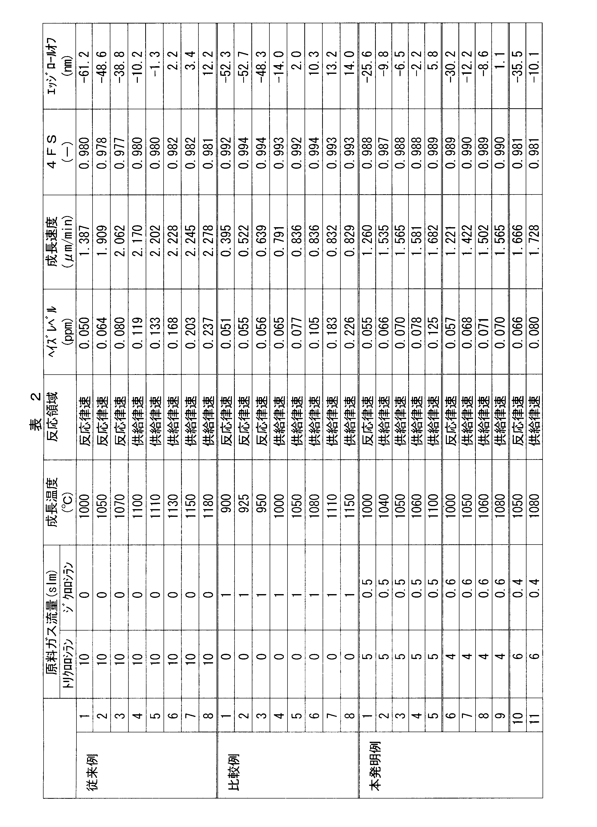
- the epitaxial growth temperature is set to various temperatures within the range of 1000 ° C. to 1100 ° C., and the epitaxial wafers obtained by epitaxial growth at the respective growth temperatures are dependent on haze level, edge roll-off, and growth rate orientation ( 4FS), as well as the epitaxial growth rate.
- the haze level was 4 to 6 of the conventional example (trichlorosilane was used as the source gas and the epitaxial growth temperature was In the range corresponding to the haze level in the polished wafer (0.050 to 0.080 ppm), or it is clearly lower than the conventional epitaxial growth conditions of 1100 ° C. to 1130 ° C. It has been reduced to a close value. However, in a high temperature region exceeding 1080 ° C., a deterioration tendency was observed depending on the mixing ratio of trichlorosilane and dichlorosilane.
- the edge roll-off is deteriorated in the reaction rate-determining region where the epitaxial growth temperature is 1000 ° C., but is maintained within a low range ( ⁇ 20 nm to +20 nm) which is almost equal to the current edge roll-off Has been. Also, the growth rate orientation dependency (4FS) was improved compared to the current situation. However, when the mixing ratio of trichlorosilane was high, no improvement effect was observed.
- the epitaxial growth rate is greatly reduced in Comparative Examples 1 to 8 using only dichlorosilane as a source gas as compared with the conventional example using trichlorosilane, but the degree of reduction is remarkably increased in Examples 1 to 11 of the present invention. It has been eased.
- a desirable temperature range for epitaxial growth is 1040 to 1080 ° C.
- the mixing ratio of trichlorosilane and dichlorosilane is 0.10 to 0.15 of dichlorosilane with respect to 1 part of trichlorosilane.
- Parts ratio (within the range of “5 parts of trichlorosilane: 0.5 part of dichlorosilane” to “4 parts of trichlorosilane: 0.6 part of dichlorosilane”), and the temperature range of epitaxial growth is controlled by supply. If the embodiment of the region is adopted (Invention Examples 2 to 4, 7 to 9), the haze level, the flatness evaluated by edge roll-off, and the growth rate orientation dependency (4FS) are all good An epitaxial wafer can be manufactured.
- a dichlorosilane was used as a source gas, and a silicon layer was epitaxially grown on the surface of a silicon wafer having a diameter of 300 mm by a CVD method.
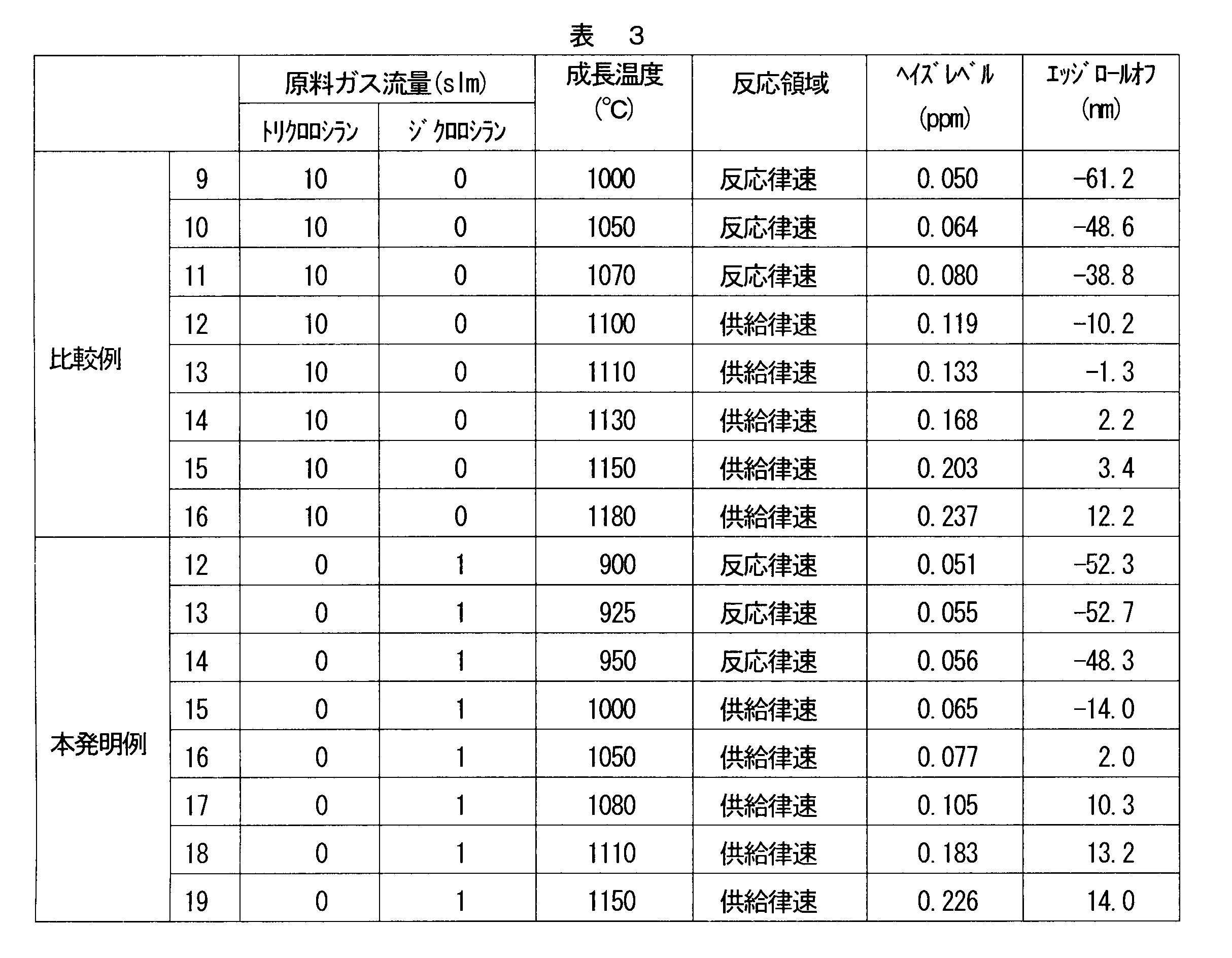
- the epitaxial growth temperature was set to various temperatures within the range of 900 ° C. to 1150 ° C., and the haze level and the edge roll-off were measured for the epitaxial wafers obtained by epitaxial growth at the respective growth temperatures.
- the supply flow rate (raw material gas flow rate) of dichlorosilane into the CVD furnace was 1 slm. This flow rate is a flow rate included in a flow rate range obtained as a flow rate capable of maintaining the edge roll-off low by a test performed in advance (see FIG. 4).
- the haze level is low and within the range corresponding to the haze level in a polished wafer (0.050 to 0.080 ppm), or It has dropped to a value close to that. However, a tendency to deteriorate was observed in a high temperature region of 1080 ° C. or higher.
- a desirable temperature range for epitaxial growth is 1000 to 1050 ° C. (Invention Examples 15 and 16).
- the haze level in this case is the haze level of a polished wafer. Equivalent to level.
- the haze level in this case is clearly lower than in Comparative Examples 12 to 14 (corresponding to the conventional epitaxial growth conditions in which trichlorosilane is used as the source gas and the epitaxial growth temperature is 1100 ° C. to 1130 ° C.). You can see that
- the edge roll-off is deteriorated in the reaction rate-determining region where the epitaxial growth temperature is 900 to 950 ° C., but within a low range ( ⁇ 14 nm to +14 nm) which is almost the same as the current edge roll-off. Is maintained.
- the edge roll-off is compared with the edge roll-off in Comparative Examples 12 to 14 corresponding to the conventional epitaxial growth conditions. It was equivalent.
- the silicon layer may be epitaxially grown on the surface of the silicon wafer within a temperature control range of ⁇ 1150 ° C., preferably a dichlorosilane supply rate-limiting region (1000 to 1150 ° C.), more preferably 1000 to 1050 ° C.
- Example in the “third invention” A dichlorosilane was used as a source gas, and a silicon layer was epitaxially grown on the surface of a silicon wafer having a diameter of 300 mm by a CVD method.
- the epitaxial growth temperature is set to various temperatures within the range of 900 ° C. to 1150 ° C., and the epitaxial wafers obtained by epitaxial growth at the respective growth temperatures are measured for the orientation dependency (4FS) of the epitaxial growth rate, In addition, edge roll-off was measured.
- 4FS orientation dependency
- the supply flow rate (raw material gas flow rate) of dichlorosilane into the CVD furnace was 1 slm. This flow rate is a flow rate included in a flow rate range obtained as a flow rate capable of maintaining the edge roll-off low by a test performed in advance (see FIG. 4).
- Table 4 shows the survey results.
- “4FS” is an evaluation of the orientation dependence of the epitaxial growth rate based on the epitaxial film thickness in the direction of 45 ° from the reference crystal orientation (0 °), and the epitaxial film thickness in the direction of 45 ° from the reference crystal orientation. Is shown as a relative film thickness when the epitaxial film thickness in the reference crystal orientation is 1.
- the relative film thicknesses are all 0.985 or more, and the growth rate orientation dependency (4FS) is the current state. It is greatly reduced from (0.985).
- the desirable temperature range for epitaxial growth is 1000 to 1050 ° C. (Examples 23 to 27 of the present invention).
- the growth rate orientation dependency (4FS) In addition to a significant reduction in, edge roll-off can be maintained at a low value of -14 nm to +14 nm. Furthermore, the edge roll-off can be set to +2 nm by selecting, for example, 1050 ° C. as the epitaxial growth temperature.
- inventive examples 20 to 27 and the comparative examples 17 to 24 are compared, it is clear that the inventive examples are excellent in the growth rate orientation dependency (4FS) in all epitaxial growth temperature ranges.
- inventive example 24 and the comparative examples 21 to 23 show the same low value, but the epitaxial growth temperature at that time is considerably lower in the inventive example 24.
- the temperature rise and temperature drop times during the epitaxial growth can be shortened, so that the productivity can be improved and the CVD reactor can be improved.
- the orientation dependence of the epitaxial growth rate is obtained by using dichlorosilane as a source gas and epitaxially growing a silicon layer on the surface of a silicon wafer within a temperature range of 900 to 1150 ° C., preferably 1000 to 1150 ° C. It has been confirmed that an epitaxial wafer with reduced edge roll-off can be produced by appropriately adjusting the raw material gas flow rate and the like.
- an epitaxial wafer having a low haze level, excellent flatness, or further reduced growth rate orientation dependency is manufactured.
- dichlorosilane the reduction of the epitaxial growth rate can be kept within a certain range, and the production efficiency of the epitaxial wafer can be kept relatively high.
- the epitaxial wafer of the present invention (first, second and third inventions) can be manufactured by the method of the present invention, and has a low haze level, so that it does not hinder measurement of fine particles and is highly integrated. It can be suitably used as a substrate material for a semiconductor device. In addition, since the edge roll-off and the growth rate orientation dependency are kept low, the device can be manufactured in a wide area, and a good device manufacturing yield can be secured.
- the present invention (the first, second and third inventions) can be widely used in the manufacture of silicon wafers and semiconductor devices.
Landscapes
- Chemical & Material Sciences (AREA)
- Engineering & Computer Science (AREA)
- Materials Engineering (AREA)
- Metallurgy (AREA)
- Organic Chemistry (AREA)
- General Chemical & Material Sciences (AREA)
- Chemical Kinetics & Catalysis (AREA)
- Crystallography & Structural Chemistry (AREA)
- Inorganic Chemistry (AREA)
- Mechanical Engineering (AREA)
- Chemical Vapour Deposition (AREA)
Abstract
Description
前述の通り、本発明者は、ジクロロシランはトリクロロシランに比べてより低温で分解するので、エピタキシャル成長温度領域を、トリクロロシランを使用する場合よりも低温化することが可能であることから、CVD法によりシリコン基板上にシリコンをエピタキシャル成長させるシリコンエピタキシャルウェーハの製造において、ジクロロシランを原料ガスとして使用することを試みた。
(a)ヘイズレベルは、原料ガスの種類や、それらの混合比によらず、エピタキシャル成長温度が1050℃以上になると急激に高くなる。
「第1の発明」で説明したと同様の着想の下に、ジクロロシランを原料ガスとして使用し、エピタキシャル成長温度を広範囲で変更して得られたエピタキシャルウェーハのヘイズレベルを測定した結果、ジクロロシランを使用することにより、ヘイズレベルをポリッシュドウェーハ(鏡面研磨したウェーハ)のヘイズレベルよりも悪化させず、良好に維持することが可能であることを確認した。
「第1の発明」で説明したと同様の着想の下に、本発明者は、CVD法によりシリコン基板上にシリコンをエピタキシャル成長させるエピタキシャルウェーハの製造において、ジクロロシランを原料ガスとして使用することを検討した。
第1の発明のエピタキシャルウェーハの製造方法(実施形態を含む)によれば、エピタキシャル成長温度をトリクロロシラン使用の場合よりも低下させ得るので、ヘイズレベルを低くすることができ、エッジロールオフが低く維持され平坦度に優れたエピタキシャルウェーハ、または、さらに成長速度方位依存性が低減されたエピタキシャルウェーハを製造することができる。ジクロロシランを使用することによるエピタキシャル成長速度の低下を一定範囲内にとどめ、エピタキシャルウェーハの生産効率を比較的良好に維持することができる。
第2の発明のエピタキシャルウェーハの製造方法(実施形態を含む)は、原料ガスとしてジクロロシランを使用し、エピタキシャル成長温度と、得られるエピタキシャルウェーハの品質特性(ヘイズレベルおよびエッジロールオフで評価される平坦度)を規定した製造方法である。
第3の発明のエピタキシャルウェーハの製造方法(実施形態を含む)は、原料ガスとしてジクロロシランを使用し、エピタキシャル成長温度と、得られるエピタキシャルウェーハの品質特性(成長速度方位依存性、さらに望ましくは、エッジロールオフにより評価される平坦度)を規定した製造方法である。
第1の発明のエピタキシャルウェーハの製造方法は、前記のとおり、シリコンウェーハの表面にシリコン層をエピタキシャル成長させるエピタキシャルウェーハの製造方法において、原料ガスとしてトリクロロシランとジクロロシランの混合ガスを使用し、1000~1100℃の温度範囲内でエピタキシャル成長させ、得られるエピタキシャルウェーハのヘイズレベルをポリッシュドウェーハのヘイズレベルよりも悪化させず、かつ平坦度に優れたものとすることを特徴とする。
第2の発明のエピタキシャルウェーハの製造方法は、前記のとおり、シリコンウェーハの表面にシリコン層をエピタキシャル成長させるエピタキシャルウェーハの製造方法において、原料ガスとしてジクロロシランを使用し、900~1150℃の温度範囲内でエピタキシャル成長させ、得られるエピタキシャルウェーハのヘイズレベルをポリッシュドウェーハのヘイズレベルよりも悪化させず、かつ平坦度に優れたものとすることを特徴とする。
第3の発明のエピタキシャルウェーハの製造方法は、前記のとおり、シリコンウェーハの表面にシリコン層をエピタキシャル成長させるエピタキシャルウェーハの製造方法において、原料ガスとしてジクロロシランを使用し、900~1150℃の温度範囲内でエピタキシャル成長させ、得られるエピタキシャルウェーハの成長速度方位依存性を低減させることを特徴とする。

原料ガスとしてトリクロロシランとジクロロシランの混合ガスを使用し、CVD法により、直径300mmのシリコンウェーハの表面にシリコン層をエピタキシャル成長させた。その際、エピタキシャル成長温度を1000℃から1100℃の範囲内の種々の温度に設定し、それぞれの成長温度でエピタキシャル成長させて得られたエピタキシャルウェーハについて、ヘイズレベル、エッジロールオフおよび成長速度方位依存性(4FS)、ならびにエピタキシャル成長速度を測定した。
原料ガスとしてジクロロシランを使用し、CVD法により、直径300mmのシリコンウェーハの表面にシリコン層をエピタキシャル成長させた。その際、エピタキシャル成長温度を900℃から1150℃の範囲内の種々の温度に設定し、それぞれの成長温度でエピタキシャル成長させて得られたエピタキシャルウェーハについて、ヘイズレベルおよびエッジロールオフを測定した。
原料ガスとしてジクロロシランを使用し、CVD法により、直径300mmのシリコンウェーハの表面にシリコン層をエピタキシャル成長させた。その際、エピタキシャル成長温度を900℃から1150℃の範囲内の種々の温度に設定し、それぞれの成長温度でエピタキシャル成長させて得られたエピタキシャルウェーハについて、エピタキシャル成長速度の方位依存性(4FS)を測定し、さらに、エッジロールオフを測定した。

Claims (27)
- シリコンウェーハの表面にシリコン層をエピタキシャル成長させるエピタキシャルウェーハの製造方法において、
原料ガスとしてトリクロロシランとジクロロシランの混合ガスを使用し、1000~1100℃の温度範囲内でエピタキシャル成長させ、
得られるエピタキシャルウェーハのヘイズレベルをポリッシュドウェーハのヘイズレベルよりも悪化させず、かつ平坦度に優れたものとすることを特徴とするエピタキシャルウェーハの製造方法。 - さらに、得られるウェーハのエピタキシャル成長速度の方位依存性を低減させることを特徴とする請求項1に記載のエピタキシャルウェーハの製造方法。
- トリクロロシランとジクロロシランの混合比を、体積比で、トリクロロシラン1部に対しジクロロシランを0.066~0.15部とすることを特徴とする請求項1または2に記載のエピタキシャルウェーハの製造方法。
- 前記エピタキシャル成長の温度領域を供給律速領域とすることを特徴とする請求項1~3のいずれかに記載のエピタキシャルウェーハの製造方法。
- 前記エピタキシャル成長の温度領域を1040~1080℃の温度範囲内とし、
得られるエピタキシャルウェーハのヘイズレベルを、KLA-Tencor社製パーティクルカウンター(SP-1)によりDWNモードで測定した場合に、0.050~0.080ppmとし、かつ、平坦度を、エッジロールオフが-20nmから+20nmの範囲内となるように向上させることを特徴とする請求項1~4のいずれかに記載のエピタキシャルウェーハの製造方法。 - さらに、前記エピタキシャル成長速度の方位依存性を基準結晶方位から45°の方位におけるエピタキシャル層の膜厚により評価する場合、基準結晶方位におけるエピタキシャル層の膜厚を1としたとき、前記45°の方位におけるエピタキシャル層の膜厚を0.985以上とすることを特徴とする請求項5に記載のエピタキシャルウェーハの製造方法。
- 前記シリコン層をエピタキシャル成長させる際の成長速度を1.5μm/minよりも大きくすることを特徴とする請求項1~6のいずれかに記載のエピタキシャルウェーハの製造方法。
- シリコンウェーハの表面にシリコン層をエピタキシャル成長させるエピタキシャルウェーハの製造方法において、
原料ガスとしてジクロロシランを使用し、900~1150℃の温度範囲内でエピタキシャル成長させ、
得られるエピタキシャルウェーハのヘイズレベルをポリッシュドウェーハのヘイズレベルよりも悪化させず、かつ平坦度に優れたものとすることを特徴とするエピタキシャルウェーハの製造方法。 - 前記エピタキシャル成長の温度領域を供給律速領域とすることを特徴とする請求項8に記載のエピタキシャルウェーハの製造方法。
- 前記エピタキシャル成長の温度領域を1000~1050℃の温度範囲内とし、
得られるエピタキシャルウェーハのヘイズレベルを、KLA-Tencor社製パーティクルカウンター(SP-1)によりDWNモードで測定した場合に、0.050~0.080ppmとし、かつ、平坦度を、エッジロールオフが-14nmから+14nmの範囲内となるように向上させることを特徴とする請求項8または9に記載のエピタキシャルウェーハの製造方法。 - 前記エピタキシャル成長の前に、シリコンウェーハにプレアニール処理を施すことを特徴とする請求項8~10のいずれかに記載のエピタキシャルウェーハの製造方法。
- 前記プレアニール処理を、エピタキシャル成長温度よりも高い温度で行うことを特徴とする請求項11に記載のエピタキシャルウェーハの製造方法。
- シリコンウェーハの表面にシリコン層をエピタキシャル成長させるエピタキシャルウェーハの製造方法において、
原料ガスとしてジクロロシランを使用し、900~1150℃の温度範囲内でエピタキシャル成長させ、
得られるウェーハのエピタキシャル成長速度の方位依存性を低減させることを特徴とするエピタキシャルウェーハの製造方法。 - 前記エピタキシャル成長速度の方位依存性を基準結晶方位から45°の方位におけるエピタキシャル層の膜厚により評価する場合、基準結晶方位におけるエピタキシャル層の膜厚を1としたとき、前記45°の方位におけるエピタキシャル層の膜厚を0.985以上とすることを特徴とする請求項13に記載のエピタキシャルウェーハの製造方法。
- 前記エピタキシャル成長温度範囲を1000~1150℃とし、
かつ、得られるエピタキシャルウェーハのエッジロールオフで評価される平坦度を、現状と同程度もしくはそれ以上に優れたものとすることを特徴とする請求項13または14に記載のエピタキシャルウェーハの製造方法。 - 前記エピタキシャルウェーハの平坦度が、エッジロールオフで-14nmから+14nmの範囲内であることを特徴とする請求項15に記載のエピタキシャルウェーハの製造方法。
- 前記エピタキシャル成長の前に、シリコンウェーハにプレアニール処理を施すことを特徴とする請求項13~16のいずれかに記載のエピタキシャルウェーハの製造方法。
- 前記プレアニール処理を、エピタキシャル成長温度よりも高い温度で行うことを特徴とする請求項17に記載のエピタキシャルウェーハの製造方法。
- 原料ガスとしてトリクロロシランとジクロロシランの混合ガスを使用し、シリコンウェーハの表面にシリコン層をエピタキシャル成長させたエピタキシャルウェーハであって、
当該ウェーハのヘイズレベルがポリッシュドウェーハのヘイズレベルと同等であり、かつ平坦度に優れていることを特徴とするエピタキシャルウェーハ。 - さらに、当該ウェーハにおけるエピタキシャル成長速度の方位依存性が低減されていることを特徴とする請求項19に記載のエピタキシャルウェーハ。
- 前記ヘイズレベルが、KLA-Tencor社製パーティクルカウンター(SP-1)によるDWNモードでの測定で、0.050~0.080ppmであり、
前記平坦度が、エッジロールオフで-20nmから+20nmの範囲内であることを特徴とする請求項19または20に記載のエピタキシャルウェーハ。 - 前記エピタキシャル成長速度の方位依存性を基準結晶方位から45°の方位におけるエピタキシャル層の膜厚により評価する場合、基準結晶方位におけるエピタキシャル層の膜厚を1としたとき、前記45°の方位におけるエピタキシャル層の膜厚が0.985以上であることを特徴とする請求項21に記載のエピタキシャルウェーハ。
- 原料ガスとしてジクロロシランを使用し、シリコンウェーハの表面にシリコン層をエピタキシャル成長させたエピタキシャルウェーハであって、
当該ウェーハのヘイズレベルがポリッシュドウェーハのヘイズレベルと同等であり、かつ平坦度に優れていることを特徴とするエピタキシャルウェーハ。 - 前記ヘイズレベルが、KLA-Tencor社製パーティクルカウンター(SP-1)によるDWNモードでの測定で、0.050~0.080ppmであり、
前記平坦度が、エッジロールオフで-14nmから+14nmの範囲内であることを特徴とする請求項23に記載のエピタキシャルウェーハ。 - 原料ガスとしてジクロロシランを使用し、シリコンウェーハの表面にシリコン層をエピタキシャル成長させたエピタキシャルウェーハであって、
当該ウェーハの成長速度方位依存性が低減されていることを特徴とするエピタキシャルウェーハ。 - 当該ウェーハのエピタキシャル成長速度の方位依存性を基準結晶方位から45°の方位におけるエピタキシャル層の膜厚により評価する場合、基準結晶方位におけるエピタキシャル層の膜厚を1としたとき、前記45°の方位におけるエピタキシャル層の膜厚が0.985以上であることを特徴とする請求項25に記載のエピタキシャルウェーハ。
- さらに、当該ウェーハの平坦度が、エッジロールオフで-14nmから+14nmの範囲内であることを特徴とする請求項25または26に記載のエピタキシャルウェーハ。
Priority Applications (3)
| Application Number | Priority Date | Filing Date | Title |
|---|---|---|---|
| KR1020127001399A KR101408913B1 (ko) | 2009-07-08 | 2010-07-08 | 에피택셜 웨이퍼 및 그 제조 방법 |
| US13/380,982 US8753962B2 (en) | 2009-07-08 | 2010-07-08 | Method for producing epitaxial wafer |
| DE112010004362T DE112010004362T5 (de) | 2009-07-08 | 2010-07-08 | Epitaxialwafer und verfahren zur herstellung desselben |
Applications Claiming Priority (8)
| Application Number | Priority Date | Filing Date | Title |
|---|---|---|---|
| JP2009-161572 | 2009-07-08 | ||
| JP2009161675A JP5453967B2 (ja) | 2009-07-08 | 2009-07-08 | エピタキシャルウェーハおよびその製造方法 |
| JP2009-161675 | 2009-07-08 | ||
| JP2009161572A JP5434317B2 (ja) | 2009-07-08 | 2009-07-08 | エピタキシャルウェーハの製造方法 |
| JP2009172633 | 2009-07-24 | ||
| JP2009-172633 | 2009-07-24 | ||
| JP2010154603A JP5516158B2 (ja) | 2009-07-24 | 2010-07-07 | エピタキシャルウェーハの製造方法 |
| JP2010-154603 | 2010-07-07 |
Publications (1)
| Publication Number | Publication Date |
|---|---|
| WO2011004602A1 true WO2011004602A1 (ja) | 2011-01-13 |
Family
ID=43429030
Family Applications (1)
| Application Number | Title | Priority Date | Filing Date |
|---|---|---|---|
| PCT/JP2010/004446 Ceased WO2011004602A1 (ja) | 2009-07-08 | 2010-07-08 | エピタキシャルウェーハおよびその製造方法 |
Country Status (4)
| Country | Link |
|---|---|
| US (1) | US8753962B2 (ja) |
| KR (1) | KR101408913B1 (ja) |
| DE (1) | DE112010004362T5 (ja) |
| WO (1) | WO2011004602A1 (ja) |
Families Citing this family (5)
| Publication number | Priority date | Publication date | Assignee | Title |
|---|---|---|---|---|
| JP5799935B2 (ja) * | 2012-11-13 | 2015-10-28 | 株式会社Sumco | 半導体エピタキシャルウェーハの製造方法、半導体エピタキシャルウェーハ、および固体撮像素子の製造方法 |
| DE102015224446A1 (de) | 2015-12-07 | 2017-06-08 | Siltronic Ag | Verfahren zur Herstellung einer epitaxierten Halbleiterscheibe |
| JP6500792B2 (ja) * | 2016-01-25 | 2019-04-17 | 株式会社Sumco | エピタキシャルウェーハの品質評価方法および製造方法 |
| DE102018221605A1 (de) | 2018-12-13 | 2020-06-18 | Siltronic Ag | Verfahren zur Herstellung einer epitaxierten Halbleiterscheibe |
| CN114188212B (zh) * | 2021-12-03 | 2026-02-06 | 上海新昇半导体科技有限公司 | 一种半导体衬底及其形成方法 |
Citations (5)
| Publication number | Priority date | Publication date | Assignee | Title |
|---|---|---|---|---|
| JP2002050579A (ja) * | 2000-05-25 | 2002-02-15 | Wacker Siltronic G Fuer Halbleitermaterialien Ag | 半導体基板の製造方法及びその使用 |
| JP2003526731A (ja) * | 1998-01-13 | 2003-09-09 | アプライド マテリアルズ インコーポレイテッド | Cvdコールドウォールチャンバおよび排気ラインの清浄方法 |
| JP2005019898A (ja) * | 2003-06-27 | 2005-01-20 | Denso Corp | 半導体基板およびその製造方法 |
| WO2008013032A1 (fr) * | 2006-07-25 | 2008-01-31 | Shin-Etsu Handotai Co., Ltd. | Procédé de fabrication d'un substrat semi-conducteur |
| JP2009111296A (ja) * | 2007-10-31 | 2009-05-21 | Sumco Corp | エピタキシャル膜形成装置用のサセプタ、エピタキシャル膜形成装置、エピタキシャルウェーハ及びエピタキシャルウェーハの製造方法 |
Family Cites Families (3)
| Publication number | Priority date | Publication date | Assignee | Title |
|---|---|---|---|---|
| JP4726272B2 (ja) | 1998-06-16 | 2011-07-20 | Sumco Techxiv株式会社 | エピタキシャルウェハの製造方法 |
| JP3849547B2 (ja) | 2002-02-28 | 2006-11-22 | 信越半導体株式会社 | 半導体エピタキシャルウェーハの測定方法、半導体エピタキシャルウェーハの測定装置、半導体エピタキシャルウェーハの製造方法及びコンピュータプログラム |
| US7332417B2 (en) | 2003-01-27 | 2008-02-19 | Amberwave Systems Corporation | Semiconductor structures with structural homogeneity |
-
2010
- 2010-07-08 WO PCT/JP2010/004446 patent/WO2011004602A1/ja not_active Ceased
- 2010-07-08 DE DE112010004362T patent/DE112010004362T5/de not_active Ceased
- 2010-07-08 KR KR1020127001399A patent/KR101408913B1/ko active Active
- 2010-07-08 US US13/380,982 patent/US8753962B2/en active Active
Patent Citations (5)
| Publication number | Priority date | Publication date | Assignee | Title |
|---|---|---|---|---|
| JP2003526731A (ja) * | 1998-01-13 | 2003-09-09 | アプライド マテリアルズ インコーポレイテッド | Cvdコールドウォールチャンバおよび排気ラインの清浄方法 |
| JP2002050579A (ja) * | 2000-05-25 | 2002-02-15 | Wacker Siltronic G Fuer Halbleitermaterialien Ag | 半導体基板の製造方法及びその使用 |
| JP2005019898A (ja) * | 2003-06-27 | 2005-01-20 | Denso Corp | 半導体基板およびその製造方法 |
| WO2008013032A1 (fr) * | 2006-07-25 | 2008-01-31 | Shin-Etsu Handotai Co., Ltd. | Procédé de fabrication d'un substrat semi-conducteur |
| JP2009111296A (ja) * | 2007-10-31 | 2009-05-21 | Sumco Corp | エピタキシャル膜形成装置用のサセプタ、エピタキシャル膜形成装置、エピタキシャルウェーハ及びエピタキシャルウェーハの製造方法 |
Also Published As
| Publication number | Publication date |
|---|---|
| KR20120024981A (ko) | 2012-03-14 |
| US20120104565A1 (en) | 2012-05-03 |
| KR101408913B1 (ko) | 2014-06-17 |
| US8753962B2 (en) | 2014-06-17 |
| DE112010004362T5 (de) | 2012-12-13 |
Similar Documents
| Publication | Publication Date | Title |
|---|---|---|
| US12467159B2 (en) | P-type SiC epitaxial wafer and production method therefor | |
| JP5134358B2 (ja) | 半導体膜の改良された堆積方法 | |
| US10774444B2 (en) | Method for producing SiC epitaxial wafer including forming epitaxial layer under different conditions | |
| WO2011004602A1 (ja) | エピタキシャルウェーハおよびその製造方法 | |
| JP6149931B2 (ja) | 炭化珪素半導体装置の製造方法および炭化珪素半導体装置 | |
| US11075114B2 (en) | Method of manufacturing semiconductor device, substrate processing apparatus, and recording medium | |
| JP2003517726A (ja) | 緩和シリコンゲルマニウム層の作製方法 | |
| TW201413074A (zh) | 磊晶矽晶圓的製造方法以及磊晶矽晶圓 | |
| JP5516158B2 (ja) | エピタキシャルウェーハの製造方法 | |
| JP4899445B2 (ja) | エピタキシャルウェーハの製造方法及びエピタキシャルウェーハ | |
| TWI459443B (zh) | Semiconductor substrate manufacturing method | |
| JP5151674B2 (ja) | エピタキシャルウエーハの製造方法 | |
| WO2023013696A1 (ja) | 半導体基板、半導体ウエハ、及び半導体ウエハの製造方法 | |
| JP5453967B2 (ja) | エピタキシャルウェーハおよびその製造方法 | |
| JP5434317B2 (ja) | エピタキシャルウェーハの製造方法 | |
| JP2008047785A (ja) | 半導体装置の製造方法 | |
| JP5316487B2 (ja) | シリコンエピタキシャルウェーハの製造方法 | |
| JP7151664B2 (ja) | エピタキシャルウェーハの製造方法 | |
| JP2021082641A (ja) | エピタキシャルウェーハの製造方法及びエピタキシャルウェーハ | |
| JP2005109149A (ja) | 半導体ウエハの製造方法 | |
| JP5877500B2 (ja) | シリコンエピタキシャルウェーハの製造方法 | |
| JP2024066211A (ja) | 多結晶SiC成形体及びその製造方法 | |
| WO2026071257A1 (ja) | SiCエピタキシャルウェハ及びSiCデバイス |
Legal Events
| Date | Code | Title | Description |
|---|---|---|---|
| 121 | Ep: the epo has been informed by wipo that ep was designated in this application |
Ref document number: 10796913 Country of ref document: EP Kind code of ref document: A1 |
|
| WWE | Wipo information: entry into national phase |
Ref document number: 13380982 Country of ref document: US |
|
| WWE | Wipo information: entry into national phase |
Ref document number: 112010004362 Country of ref document: DE Ref document number: 1120100043620 Country of ref document: DE |
|
| ENP | Entry into the national phase |
Ref document number: 20127001399 Country of ref document: KR Kind code of ref document: A |
|
| 122 | Ep: pct application non-entry in european phase |
Ref document number: 10796913 Country of ref document: EP Kind code of ref document: A1 |