WO2011002031A1 - 素子搭載用基板および半導体モジュール - Google Patents
素子搭載用基板および半導体モジュール Download PDFInfo
- Publication number
- WO2011002031A1 WO2011002031A1 PCT/JP2010/061172 JP2010061172W WO2011002031A1 WO 2011002031 A1 WO2011002031 A1 WO 2011002031A1 JP 2010061172 W JP2010061172 W JP 2010061172W WO 2011002031 A1 WO2011002031 A1 WO 2011002031A1
- Authority
- WO
- WIPO (PCT)
- Prior art keywords
- metal core
- metal
- element mounting
- mounting substrate
- film
- Prior art date
- Legal status (The legal status is an assumption and is not a legal conclusion. Google has not performed a legal analysis and makes no representation as to the accuracy of the status listed.)
- Ceased
Links
Images






Classifications
-
- H—ELECTRICITY
- H05—ELECTRIC TECHNIQUES NOT OTHERWISE PROVIDED FOR
- H05K—PRINTED CIRCUITS; CASINGS OR CONSTRUCTIONAL DETAILS OF ELECTRIC APPARATUS; MANUFACTURE OF ASSEMBLAGES OF ELECTRICAL COMPONENTS
- H05K3/00—Apparatus or processes for manufacturing printed circuits
- H05K3/44—Manufacturing insulated metal core circuits or other insulated electrically conductive core circuits
- H05K3/445—Manufacturing insulated metal core circuits or other insulated electrically conductive core circuits having insulated holes or insulated via connections through the metal core
-
- H—ELECTRICITY
- H05—ELECTRIC TECHNIQUES NOT OTHERWISE PROVIDED FOR
- H05K—PRINTED CIRCUITS; CASINGS OR CONSTRUCTIONAL DETAILS OF ELECTRIC APPARATUS; MANUFACTURE OF ASSEMBLAGES OF ELECTRICAL COMPONENTS
- H05K1/00—Printed circuits
- H05K1/02—Details
- H05K1/03—Use of materials for the substrate
- H05K1/05—Insulated conductive substrates, e.g. insulated metal substrate
-
- H—ELECTRICITY
- H10—SEMICONDUCTOR DEVICES; ELECTRIC SOLID-STATE DEVICES NOT OTHERWISE PROVIDED FOR
- H10W—GENERIC PACKAGES, INTERCONNECTIONS, CONNECTORS OR OTHER CONSTRUCTIONAL DETAILS OF DEVICES COVERED BY CLASS H10
- H10W40/00—Arrangements for thermal protection or thermal control
- H10W40/20—Arrangements for cooling
- H10W40/25—Arrangements for cooling characterised by their materials
- H10W40/255—Arrangements for cooling characterised by their materials having a laminate or multilayered structure, e.g. direct bond copper [DBC] ceramic substrates
-
- H—ELECTRICITY
- H05—ELECTRIC TECHNIQUES NOT OTHERWISE PROVIDED FOR
- H05K—PRINTED CIRCUITS; CASINGS OR CONSTRUCTIONAL DETAILS OF ELECTRIC APPARATUS; MANUFACTURE OF ASSEMBLAGES OF ELECTRICAL COMPONENTS
- H05K1/00—Printed circuits
- H05K1/02—Details
- H05K1/03—Use of materials for the substrate
- H05K1/05—Insulated conductive substrates, e.g. insulated metal substrate
- H05K1/053—Insulated conductive substrates, e.g. insulated metal substrate the metal substrate being covered by an inorganic insulating layer
-
- H—ELECTRICITY
- H05—ELECTRIC TECHNIQUES NOT OTHERWISE PROVIDED FOR
- H05K—PRINTED CIRCUITS; CASINGS OR CONSTRUCTIONAL DETAILS OF ELECTRIC APPARATUS; MANUFACTURE OF ASSEMBLAGES OF ELECTRICAL COMPONENTS
- H05K1/00—Printed circuits
- H05K1/02—Details
- H05K1/03—Use of materials for the substrate
- H05K1/05—Insulated conductive substrates, e.g. insulated metal substrate
- H05K1/056—Insulated conductive substrates, e.g. insulated metal substrate the metal substrate being covered by an organic insulating layer
-
- H—ELECTRICITY
- H05—ELECTRIC TECHNIQUES NOT OTHERWISE PROVIDED FOR
- H05K—PRINTED CIRCUITS; CASINGS OR CONSTRUCTIONAL DETAILS OF ELECTRIC APPARATUS; MANUFACTURE OF ASSEMBLAGES OF ELECTRICAL COMPONENTS
- H05K1/00—Printed circuits
- H05K1/18—Printed circuits structurally associated with non-printed electric components
- H05K1/182—Printed circuits structurally associated with non-printed electric components associated with components mounted in printed circuit boards [PCB], e.g. insert-mounted components [IMC]
- H05K1/185—Printed circuits structurally associated with non-printed electric components associated with components mounted in printed circuit boards [PCB], e.g. insert-mounted components [IMC] associated with components encapsulated in the insulating substrate of the PCBs; associated with components incorporated in internal layers of multilayer circuit boards
-
- H—ELECTRICITY
- H05—ELECTRIC TECHNIQUES NOT OTHERWISE PROVIDED FOR
- H05K—PRINTED CIRCUITS; CASINGS OR CONSTRUCTIONAL DETAILS OF ELECTRIC APPARATUS; MANUFACTURE OF ASSEMBLAGES OF ELECTRICAL COMPONENTS
- H05K2201/00—Indexing scheme relating to printed circuits covered by H05K1/00
- H05K2201/01—Dielectrics
- H05K2201/0183—Dielectric layers
- H05K2201/0195—Dielectric or adhesive layers comprising a plurality of layers, e.g. in a multilayer structure
-
- H—ELECTRICITY
- H05—ELECTRIC TECHNIQUES NOT OTHERWISE PROVIDED FOR
- H05K—PRINTED CIRCUITS; CASINGS OR CONSTRUCTIONAL DETAILS OF ELECTRIC APPARATUS; MANUFACTURE OF ASSEMBLAGES OF ELECTRICAL COMPONENTS
- H05K2201/00—Indexing scheme relating to printed circuits covered by H05K1/00
- H05K2201/06—Thermal details
- H05K2201/068—Thermal details wherein the coefficient of thermal expansion is important
-
- H—ELECTRICITY
- H10—SEMICONDUCTOR DEVICES; ELECTRIC SOLID-STATE DEVICES NOT OTHERWISE PROVIDED FOR
- H10W—GENERIC PACKAGES, INTERCONNECTIONS, CONNECTORS OR OTHER CONSTRUCTIONAL DETAILS OF DEVICES COVERED BY CLASS H10
- H10W72/00—Interconnections or connectors in packages
- H10W72/50—Bond wires
- H10W72/551—Materials of bond wires
- H10W72/552—Materials of bond wires comprising metals or metalloids, e.g. silver
-
- H—ELECTRICITY
- H10—SEMICONDUCTOR DEVICES; ELECTRIC SOLID-STATE DEVICES NOT OTHERWISE PROVIDED FOR
- H10W—GENERIC PACKAGES, INTERCONNECTIONS, CONNECTORS OR OTHER CONSTRUCTIONAL DETAILS OF DEVICES COVERED BY CLASS H10
- H10W74/00—Encapsulations, e.g. protective coatings
-
- H—ELECTRICITY
- H10—SEMICONDUCTOR DEVICES; ELECTRIC SOLID-STATE DEVICES NOT OTHERWISE PROVIDED FOR
- H10W—GENERIC PACKAGES, INTERCONNECTIONS, CONNECTORS OR OTHER CONSTRUCTIONAL DETAILS OF DEVICES COVERED BY CLASS H10
- H10W90/00—Package configurations
- H10W90/701—Package configurations characterised by the relative positions of pads or connectors relative to package parts
- H10W90/721—Package configurations characterised by the relative positions of pads or connectors relative to package parts of bump connectors
- H10W90/724—Package configurations characterised by the relative positions of pads or connectors relative to package parts of bump connectors between a chip and a stacked insulating package substrate, interposer or RDL
-
- H—ELECTRICITY
- H10—SEMICONDUCTOR DEVICES; ELECTRIC SOLID-STATE DEVICES NOT OTHERWISE PROVIDED FOR
- H10W—GENERIC PACKAGES, INTERCONNECTIONS, CONNECTORS OR OTHER CONSTRUCTIONAL DETAILS OF DEVICES COVERED BY CLASS H10
- H10W90/00—Package configurations
- H10W90/701—Package configurations characterised by the relative positions of pads or connectors relative to package parts
- H10W90/751—Package configurations characterised by the relative positions of pads or connectors relative to package parts of bond wires
- H10W90/754—Package configurations characterised by the relative positions of pads or connectors relative to package parts of bond wires between a chip and a stacked insulating package substrate, interposer or RDL
Definitions
- the present invention relates to an element mounting substrate and a semiconductor module in which a semiconductor element is mounted on the element mounting substrate.
- FIG. 7 illustrates a semiconductor device 100 that employs an element mounting substrate having a metal core.
- 7A is a plan view of the semiconductor device
- FIG. 7B is a cross-sectional view of the semiconductor device along the line A-A ′.
- This element mounting substrate employs a metal core 101 at the center of the core, the front side is covered with an insulating resin 102A, and the back side is covered with an insulating resin 102B.
- Conductive patterns 103A and 103B are provided.
- the insulating resin layers 102A and 102B and the conductive patterns 103A and 103B are formed on the front and back surfaces, respectively, but the conductive patterns may be further laminated with four layers, six layers, and so on.
- a semiconductor element 104 such as an LSI is fixed to the element mounting board via solder balls 106 formed corresponding to the conductive pattern 103A, and covers the semiconductor element 104 leaving the periphery of the element mounting board.
- the semiconductor device 100 is formed by being sealed with the insulating resin film 105.
- the heat generated from the semiconductor element 104 is diffused through the metal core 101, so that the temperature of the semiconductor element 04 is reduced.
- the semiconductor element 104 is mounted face down in order to reduce the thickness of the entire semiconductor device 100 as much as possible.
- the heat generated from the semiconductor element 104 is Since it is discharged to the metal core 101 through the solder ball 106 and the conductive pattern 103A, the temperature of the semiconductor element 104 is unlikely to decrease. That is, since the heat flow from the semiconductor element 104 is restricted by the solder ball 106 that is the neck portion, the temperature of the semiconductor element 104 is unlikely to decrease.
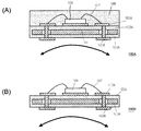
- FIG. 8 shows a semiconductor device (semiconductor module) on which a semiconductor element is mounted.
- FIG. 8A shows the structure of a semiconductor module 100A in which the semiconductor element 104 is mounted face up. Because of the face-up mounting, the semiconductor module 100A itself becomes thicker by the height of the thin metal wire 107. However, since the back surface of the semiconductor element 104 is fixed in a large area as compared with the case where the back surface of the semiconductor element 104 is connected to the element mounting substrate with solder balls, the temperature of the semiconductor element 104 is higher than that in the case of mounting the semiconductor element in FIG. Decrease significantly.
- FIG. 8B shows the semiconductor module 100B not covered with the insulating resin film 105, and a passive element such as a semiconductor element or a chip capacitor is mounted on the element mounting substrate.
- the semiconductor element 104 uses a thin metal wire, but it may be fixed via a bump as shown in FIG.
- a metal core substrate As described above, in a thin package or module that employs a substrate, when heat dissipation is required, it is preferable to employ a metal core substrate.
- Cu is mainly used as the metal core, and its thickness is about 250 ⁇ m to 500 ⁇ m. Therefore, even if the conductive pattern has two layers or four layers, since the thickness is about 1 mm, the metal core is easily plastically deformed. Further, once the metal is plastically deformed, it cannot be restored unless it is deformed again in the opposite direction, which leads to a decrease in yield in the manufacturing process. Further, in the finished product, the reliability is lowered. Furthermore, the difference in the thermal expansion coefficient ⁇ between the insulating resin and Cu also causes warping. In FIG.
- the respective thermal expansion coefficients of the insulating resin film are 10 to 15 ppm
- the substrate is 13 to 15 ppm in the X and Y directions
- the Z direction is 23 to 33 ppm
- Si is 2.5 ppm.
- the reliability of the semiconductor element itself is reduced. Therefore, it is desirable that the substrate be as flat as possible.
- the present invention has been made in view of the above problems, and includes a metal core mainly composed of metal, a first ceramic film formed on one main surface of the metal core, and another main core of the metal core.
- a second ceramic film formed on the surface, a first insulating resin film formed on the surface of the first ceramic film, and a second insulating resin film formed on the surface of the second ceramic film And a first conductive pattern provided on the surface of the first insulating resin film, and a second conductive pattern provided on the surface of the second insulating resin film.
- the first ceramic film and the second ceramic film are element mounting substrates characterized by having a smaller coefficient of thermal expansion and higher rigidity than the metal core.
- the ductility of the metal core substrate is prevented, Protecting the brittleness of the ceramic film by providing the first insulating resin film and the second insulating resin film coated over substantially the entire surface of the front side of the first ceramic film and the back side of the second ceramic film Can do.
- the ceramic and insulating resin are substantially formed on the front and back, centering on the metal core, warpage of the element mounting substrate can be suppressed.
- the semiconductor module and the semiconductor device mounted on the element mounting substrate can improve flatness and at the same time improve heat dissipation.
- FIG. 1 is a drawing of an element mounting substrate and a semiconductor module according to an embodiment of the present invention.
- 1 is a drawing of an element mounting substrate and a semiconductor module according to an embodiment of the present invention.
- 1 is a drawing of an element mounting substrate and a semiconductor module according to an embodiment of the present invention.
- 1 is a drawing of an element mounting substrate and a semiconductor module according to an embodiment of the present invention.
- It is a figure of the conventional semiconductor device. It is a figure of the conventional semiconductor device. It is a figure of the conventional semiconductor device. It is a figure of the conventional semiconductor device. It is a figure explaining the manufacturing method of this invention. It is a figure explaining the manufacturing method of this invention.
- the element mounting substrate 1 has a metal core substrate M including a metal core 2, a ceramic film CEa formed on the surface of the metal core 2, and a ceramic film CEb formed on the back surface.
- the ceramic film CE may be formed by attaching a ceramic material to the metal core 2 or formed by chemically treating the metal core 2.
- An insulating resin film 4A is formed on the surface of the ceramic film CEa, and an insulating resin film 4B is formed on the surface of the ceramic film CEb. Further, a conductive pattern 5A is formed on the surface of the insulating resin film 4A, and a conductive pattern 5B is formed on the surface of the insulating resin film 4B.
- the element mounting substrate shown here has a two-layered conductive pattern structure including the front and back, but is a multilayer substrate of 4, 6 layers, etc. in which the insulating resin film and the conductive pattern are repeatedly laminated. May be.
- the ceramic films CE are arranged on both sides. Since the ceramic film CE has high rigidity and is difficult to be deformed, warpage due to plastic deformation of the metal core can be prevented. On the other hand, the unique vulnerability of ceramics is solved by arranging insulating resin films on the front and back sides.
- the element mounting substrate has a ceramic film and an insulating resin layer with the same material and the same film thickness symmetrically on the front and back surfaces with the metal core as the center. For this reason, the front and back sides extend in the same way, and from this point, it is possible to prevent warping.
- the metal used as the core material for example, a material mainly composed of Cu or Al can be cited. Since Cu as the main material is excellent in heat dissipation, it is suitable for a power system module that handles a large current. On the other hand, although Al is the main material, it is inferior to Cu, but has excellent heat dissipation. In particular, in the case of Al, a film that is lighter than Cu and that is formed by self-oxidation and self-generation (aluminum oxide, alumina film) is excellent in resistance and rigidity, and therefore requires flatness and heat dissipation at once. Is preferable.
- An alumina film is desirable as the ceramic film.
- an alumina film can be formed in a self-generated manner, for example, by an anodic oxidation method.
- the alumina film formed by the anodic oxidation method is generally an amorphous film.
- ⁇ -alumina is further desirable.
- ⁇ -Alumina is excellent in chemical stability and mechanical strength due to its crystal structure, and has a large electrical insulation resistance.
- One of the methods for forming alumina is a submerged plasma method.
- the alumina film formed by the in-liquid plasma method has a fine crystal structure and thus is not brittle.
- a porous layer formed in the alumina film when formed by the anodic oxidation method does not occur, so that it is very small at the time of cutting. Alumina pieces are not easily generated. Therefore, by using alumina without a porous layer as the ceramic film formed on the surface of the metal material, it is possible to suppress the scattering of the ceramic pieces during the formation of through-holes or individualization in the subsequent steps. Manufacturing yield can be increased.
- the thickness of the ceramic film is greater than the thickness of the metal material used as the core material.
- the metal material of the inner layer is desirably 50 ⁇ m or more, and if it is thinner than this, impact resistance cannot be obtained.
- the inner layer metal material is desirably 500 ⁇ m or less. If it is thicker than this, the entire thickness of the element mounting substrate increases, which is not desirable.
- a through hole 3 is formed in the element mounting substrate 1.
- the ceramic film CE is formed by the above-described self-generated means, the ceramic film CE can be easily formed on the side wall of the through hole 3.
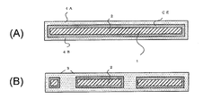
- FIG. 1A is a first embodiment of an element mounting substrate of the present invention, and is for explaining the configuration of the element mounting substrate when viewed from the cross section along the line AA in FIG.
- FIG. 1B is a perspective view of the element mounting substrate of the present invention as seen in a plan view.
- FIG. 2 shows a second embodiment of the element mounting substrate of the present invention
- FIG. 2 (A) is a sectional view of the element mounting substrate of the present invention taken along line AA in FIG. 2 (B).
- FIG. 2B is a perspective view of the element mounting substrate of the present invention as seen in a plan view.
- a single metal core substrate M is provided over the entire region of the element mounting substrate 1 or substantially the entire region except for a slight margin MG.
- the upper and lower contacts are provided with a through hole 3 in a part of one metal core substrate M, and are in contact with each other through the part. Details will be described later with reference to FIG.
- the metal core substrate M is provided except for the whole area or the margin MG, and the metal core substrate M is not a single piece as shown in FIG. It consists of a plurality of pieces of metal core substrates MA, MB.
- the plurality of metal core substrates are separated into island shapes and arranged on substantially the same plane.
- the lead-out of the front and back electrodes of the element mounting substrate is connected through a through hole 3 between the two metal cores MA and MB. Details will be described later with reference to FIG.
- the metal core 2 is made of metal or metal alloy, and has a thickness of about 50 ⁇ m to 500 ⁇ m.
- the metal core is made of Cu or Cu as a main material, or Al or Al as a main material.
- “metal is the main material” means that most of the metal material contains impurities in the order of ppm and has improved properties.
- the material of the metal core 2 is preferably Al or Al. This is because although the thermal conductivity is slightly worse than Cu, the Al material is lightweight, and the Al material can form a hard and rigid ceramic film in a self-generated manner.
- the ceramic film formed in a self-generated manner is a reaction product of a metal material formed by chemical treatment, and is, for example, an alumina film formed by anodizing treatment.
- the alumina film has high hardness, and the rigidity can be increased by the film thickness.
- the insulating resin film 4A is formed on the surface of the ceramic film CEa formed on the surface of the metal core 2, and the insulating resin film 4B is formed on the surface of the ceramic film CEb formed on the back surface of the metal core 2. Since the ceramic film CE is brittle and chipped, its surface is covered with the insulating resin film 4 to solve the drawbacks. Since the element mounting substrate 1 has increased rigidity by the ceramic film CE, the insulating resin film 4 may not be mixed with a filler. If glass fiber or the like is woven into the insulating resin film 4 or a filler is mixed in, there is a risk of generation as dust during dicing.
- a square (frame) indicated by a dotted line on the outermost periphery shown in FIGS. 1 and 2 is an outer shape of the element mounting substrate 1 and corresponds to the dicing line DC1 shown in FIGS. 4 (A) and 6 (C). To do.
- the ceramic film CE is arranged inside the dicing line DC1, and the metal core 2 is not exposed directly to the end face of the element mounting substrate 1, thereby improving the withstand voltage.
- the thick dashed line shown in FIG. Dicing is performed in a region indicated by (DC2).
- the metal core substrate M is directly exposed on the end face of the element mounting substrate 1.
- heat dissipation is excellent.
- a conductive pattern 5A is formed on the surface of the insulating resin film 4A, and a conductive pattern 5B is formed on the surface of the insulating resin film 4B.
- the conductive pattern 5A includes an island on which a semiconductor element is placed, an electrode connected to the semiconductor element, a passive element, or the like, an island, or a wiring extending integrally with the electrode.
- the conductive pattern 5B is mainly an external electrode, but the island, electrode, wiring, and the like may be provided.
- FIG. 1 shows a two-layer metal wiring structure in which the wiring layer excluding the metal core is a wiring layer 5A and a wiring layer 5B.
- the insulating resin film and the conductive pattern are repeated on the front and back sides, respectively.
- FIG. 3 illustrates an example of the structure shown in FIGS. 1A and 1B more specifically.
- 3A is a perspective view
- FIG. 3B is a cross-sectional view taken along the line AA of FIG. 3A
- FIGS. 4A and 4B illustrate the state of the metal core substrate when dicing is performed.
- FIG. 5A is a cross-sectional view showing a state in which the element EL is embedded in the element mounting substrate.
- the conductive pattern has four layers as shown in FIG. 3 (B).
- FIG. 3 (A) for example, four through holes 3 are formed in one metal core substrate M.
- One is provided.
- An element EL is embedded in the opening OP in the element mounting substrate.
- the element EL may be a semiconductor bare chip, or may be a SIP in which a plurality of semiconductor elements and passive elements are included in one package.
- SIP since the number of terminals to be connected to the electrodes of the metal core substrate is reduced, the reliability is improved. For example, when an IC bare chip and a transistor are buried with each bare, the number of IC terminals and the three terminals of the transistor are required for connection.
- the embedded element EL is arranged with a slight shift from the center.
- An alternate long and short dash line provided with an arrow at the tip shown in FIG. 3A and perpendicular to each other is a vertical and horizontal center line of the element mounting substrate, and the intersection is the center.
- the element EL is arranged so as to be shifted from the intersection which is the center.
- FIG. 4 (A) shows the separation method.
- Each metal core 2 is composed of one plate-like substrate, and the metal cores are arranged in a matrix.
- the solid line arrows arranged in the vertical direction are dicing lines.
- the metal core 2 is not directly diced, and the insulating resin film 4 existing between the metal cores 2 is diced and separated. By doing so, the cross section of the metal core 2 is not exposed to the side surface of the element mounting substrate 1 as shown in FIG. 1A and FIG. Since the ceramic film is formed, the withstand voltage characteristics are improved.
- FIG. 4 (B) shows a separation method of an embodiment different from FIG. 4 (A).
- the outer solid line indicates one metal core substrate M.
- An area where originally four element mounting substrates can be realized is prepared in advance with one metal substrate, and the metal core substrate M itself is directly diced later. In this case, it is not necessary to separate the metal core substrate M in advance as in the embodiment of FIG. Further, the metal core 2 is exposed on the side surface of the element mounting substrate 1 after dicing, and the heat dissipation is excellent.
- FIG. 6 shows another embodiment of the present invention.
- 6A is a perspective view
- FIG. 6B is a cross-sectional view taken along the line AA of FIG. 6A
- FIG. 6C is a diagram showing a state of the metal core substrate during dicing
- FIG. ) Is a cross-sectional view showing a state in which the element EL is embedded in the element mounting substrate.
- the ceramic film which is the point of the present invention, is embedded between the separated metal core substrates with the insulating resin layer 4 and covers all of the front surface, the back surface, and the side surfaces.
- the rigidity of the core substrate M is increased.
- the space between the adjacent metal core substrates M is composed of the insulating resin layer 4, the metal core substrate M is easily bent at that portion. Therefore, in the present invention, the insulating resin film 4 between the metal core substrates M adjacent to each other does not extend from one side of the element mounting substrate to the opposite side, and the metal core substrate M is formed in the middle. Arranged and configured to be blocked there.
- the insulating resin film 4 between the metal core substrate MA and the metal core substrate MB is blocked by the metal core substrate MC as indicated by an arrow A in FIG.
- the insulating resin film 4 between the metal core substrate MA and the metal core substrate MC is blocked by the metal core substrate MB as indicated by an arrow B.
- the insulating resin film 4 between the metal core substrate MC and the metal core substrate MD and the insulating resin film 4 between the metal core substrate MB and the metal core substrate MD are also indicated by arrows C and D, respectively. It is blocked by another metal core substrate M.
- the weak part of the element mounting substrate as shown in FIG.
- 6A is the extending direction of the arrow where the metal core substrate M does not exist, but halfway from one side of the element mounting substrate to the opposite side. Since the metal core substrate M is contained in the substrate, it is possible to prevent the substrate from being cracked or bent all at once from one side of the element mounting substrate to the opposite side.
- the metal core substrate MC is removed, and an element EL made of a bare chip or SIP is embedded in the element mounting substrate as shown in FIG. 6D. It is.
- the three metal core substrates MA, MC, and MD have the metal core 2 exposed at a portion indicated by a dotted circle (a contact hole in which an insulating resin is opened), and as shown in FIG. The wiring on the substrate and the metal core 2 are in contact.
- a thick arrow in FIG. 6C indicates a dicing line, and indicates that the metal core substrate is disposed so as to recede inward from the side of the element mounting substrate.
- the metal core substrate M is not exposed on the side surface of the element mounting substrate 1, and a ceramic film that is a self-generated film is formed including the side surface, so that the withstand voltage characteristics are improved. Since the structure described in FIG. 2 described above separates the metal core substrate, forms a through hole in the separation portion, and forms a via there, it is not necessary to form a hole penetrating the metal core substrate.
- the metal core substrate is used as a relay for the via, so that the metal core is electrically separated from the portion where electrical separation is required. Since the substrate can be separated, there is no need to form a hole penetrating the metal core substrate, and a fine via can be easily formed because the depth of the via becomes shallow.
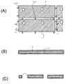
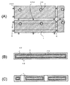
- FIG. 9A is a plan view of the metal core substrate M in the element mounting substrate manufacturing method
- FIG. 9B is a cross-sectional view taken along the line AA of FIG. 9A
- FIG. 9C is FIG. It is BB sectional drawing of (A).
- plate-like metal core substrates M provided on one element mounting substrate 1 are arranged vertically and horizontally in a plane, and are integrally formed by connecting pieces 30A and 30B extending vertically and horizontally.
- the metal core substrate M shown in FIG. 9A is formed as follows. First, the metal core 2 is formed by pressing or etching a metal sheet or metal foil. Next, as shown in FIG. 9B and FIG. 9C, a ceramic film is formed on the front surface, the back surface, and the side surface of the metal core 2 in a self-generated manner. Thus, the metal core substrate M shown in FIG. 9A is formed. At this time, the through hole 3 is formed as shown in FIG. 9C (cross section BB in FIG.
- the ceramic film CE is also formed on the inner side wall of the through hole 3.
- a self-generated film is not formed on the connecting piece corresponding to the separation line. Is preferable.
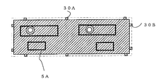
- FIG. 10A shows a state in which the insulating resin film 4 is formed on the cross section shown in FIG. 9B
- FIG. 10B shows the insulating resin film on the cross section shown in FIG. 9C
- 4 shows a state in which 4 is formed.
- the front and back surfaces of the metal core substrate are flat and covered with a ceramic film and an insulating resin film.
- the side wall of the through hole 3 is covered with a ceramic film and an insulating resin film.
- FIG. 11A is a plan view
- FIG. 11B is a cross-sectional view taken along the line AA in FIG. 11A
- FIG. 11C is a cross-sectional view taken along the line BB in FIG. 11A.
- This through hole is formed by forming the second through hole 3A having a diameter smaller than that of the through hole 3 while leaving the ceramic film and the insulating resin film 4 formed on the side wall of the through hole 3. Since the area where the second through-hole 3A is formed is composed only of an insulating resin film, it can be easily formed by laser, drilling or punching.
- the side wall of the through-hole 3 and the side wall of the metal core substrate are covered with the ceramic film and the insulating resin film in a double manner on the outside of the metal core substrate.
- a conductive material is embedded in the second through hole 3A by plating, conductive paste, solder, or the like.
- the conductive pattern 5A on the front surface and the conductive pattern 5B on the back surface of the element mounting substrate to be formed later are electrically connected.
- the electrical connection between the conductive pattern 5A and the conductive pattern 5B may be made by forming a conductive film on the side wall of the second through-hole 3A, or a conductive paste such as Ag or plating may be used for the second penetration.
- the holes 3A may be filled.
- FIG. 13 corresponds to the portion indicated by the dotted line in FIG. 9 (A) and FIG. 11 (A).
- the insulating resin layer 4 is exposed at the end face of the completed element mounting substrate, the side walls of the connecting pieces 30A and 30B are exposed at a part thereof.
- the metal material is only a narrow connecting piece portion, so that the load on the blade and the like is small, and it can be easily separated.
- a semiconductor element is mounted on the element mounting substrate to form a semiconductor module. Furthermore, the semiconductor element of the semiconductor module is sealed with an insulating resin to form a semiconductor device.
- adopted in this application is shown.
- FIG. 14 is a perspective view for explaining a method for observing the film structure of an alumina film in a plane having a perpendicular direction to the film thickness direction of an alumina film which is an example of a ceramic film
- FIG. 15 is an SEM photograph observing the film structure.
- FIG. 14A a sample in which an alumina (Al 2 O 3) film is formed on an aluminum (Al) film is prepared.
- the alumina film is cut out using FIB (Focused Ion Beam), and a plane with the film thickness direction in the alumina film as a perpendicular is exposed to the surface.
- FIG. 14B an SEM photograph of the surface is taken from the direction of the arrow.
- FIG. 15 is an SEM photograph thereof.
- FIGS. 15A and 15B are SEM photographs of an alumina film formed by using a submerged plasma method
- FIG. 15C shows an alumina film formed by an anodization method taken for comparison. It is a SEM photograph.
- FIG. 15B is a photograph taken at a larger magnification (10,000 times) of the photograph of FIG. 15A, and FIG. 15B and FIG. 15C are the same magnification (100,000 times).
- the alumina film formed by using the anodic oxidation method has a porous layer in which a large number of holes are formed on the entire surface, whereas the submerged plasma method is used. It can be seen that the alumina film formed in this manner does not have a porous layer having fine pores formed on the entire surface. From this, it can be seen that the alumina film formed by using the in-liquid plasma method is denser, has higher rigidity, and is less likely to produce minute alumina pieces. Therefore, since the alumina film formed by the submerged plasma method has high rigidity, the film thickness can be reduced, and the overall thickness of the element mounting substrate can be reduced.
- the present invention is a device mounting board that uses a core film made of a ceramic film formed on the front and back surfaces of a metal substrate, it will be mounted in a light, thin and small set in the future, realizing both high rigidity and heat dissipation. it can.
- Element mounting substrate 2 Metal core 3: Through hole 4: Insulating resin 5: Conductive pattern M: Metal core substrate MG: Margin DC: Dicing line
Landscapes
- Engineering & Computer Science (AREA)
- Microelectronics & Electronic Packaging (AREA)
- Manufacturing & Machinery (AREA)
- Structure Of Printed Boards (AREA)
- Insulated Metal Substrates For Printed Circuits (AREA)
- Chemical & Material Sciences (AREA)
- Ceramic Engineering (AREA)
Abstract
Description
半田ボール106と導電パターン103Aを介して金属コア101へと放出されることになるので、半導体素子104の温度は低下しにくい。つまり、半導体素子104からの熱流が、ネック部分である半田ボール106で規制されてしまうため、半導体素子104の温度は低下しにくいのである。
特開2004-31732号公報
特開昭63-72180号公報
前記第1のセラミック膜および前記第2のセラミック膜は、前記金属コアよりも熱膨張係数が小さくかつ、剛性が高いことを特徴とする素子搭載用基板である。
軽薄短小で放熱性が求められるセットに使われる際は、金属コア2の材料としてはAlまたはAlを主材料とするものが良い。Cuと比較して熱伝導性は若干悪いが、Al材料は軽量であり、またAl材料は硬質、剛性を持つセラミック膜を自己生成的に形成することが可能であるからである。この自己生成的に形成されるセラミック膜とは、化学的処理により形成される金属材料の反応生成物であり、例えば、陽極酸化処理により形成されるアルミナ膜である。アルミナ膜は、硬度が高く、その膜厚により剛性を高めることができる。
上述の図2において説明した構造が、金属コア基板を分離し、その分離部に貫通孔を形成してそこにビアを形成することにより、金属コア基板を貫通する孔を形成する必要が無いため、貫通孔の形成が容易であったのに対して、上述のように、本実施例によれば、金属コア基板をビアの中継として利用するため、電気的に分離が必要な箇所で金属コア基板を分離することが出来ることから、金属コア基板を貫通する孔を形成する必要がなく、またビアの深さが浅くなることから微細なビアが形成しやすくなる。
ここで、本願において採用するセラミック膜の膜構造の評価を行った結果を示す。
まず、セラミック膜の一例であるアルミナ膜の膜厚方向を垂線とする平面におけるセラミック膜の膜構造を観察する方法を説明する。
図14は、セラミック膜の一例であるアルミナ膜の膜厚方向を垂線とする平面におけるアルミナ膜の膜構造を観察する方法を説明する斜視図であり、図15は、膜構造を観察したSEM写真である。
図14(A)に示すように、アルミニウム(Al)膜上にアルミナ(Al2O3)膜を形成したサンプルを用意する。そのサンプルのうち、アルミナ膜をFIB(Focused Ion Beam:集束イオンビーム)を用いて切り出し、アルミナ膜中の膜厚方向を垂線とする平面を表面に露出させる。そして、図14(B)に示すように、その表面を矢印方向からSEM写真を撮影する。
図15が、そのSEM写真である。図15(A)及び(B)は、液中プラズマ法を用いて形成したアルミナ膜のSEM写真であり、図15(C)はその比較のために撮影した陽極酸化法によって形成したアルミナ膜のSEM写真である。なお、図15(B)は図15(A)の写真の倍率(1万倍)を大きくして撮影したものであり、図15(B)と図15(C)は同じ倍率(10万倍)で撮影したものである。
図15(C)に示すように、陽極酸化法を用いて形成したアルミナ膜には多数の孔が全面に形成されている多孔層が存在しているのに対して、液中プラズマ法を用いて形成したアルミナ膜には、全面に微細孔が形成されている多孔層が存在していないことがわかる。このことから、液中プラズマ法を用いて形成したアルミナ膜の方が緻密な膜であり剛性が高く、かつ、微小なアルミナ片が出にくいことがわかる。
よって、液中プラズマ法によって形成したアルミナ膜は剛性が高いことから、膜厚を小さくすることができ、よって素子搭載用基板の全体的な厚みを薄くすることができる。
2:金属コア
3:貫通孔
4:絶縁樹脂
5:導電パターン
M:金属コア基板
MG:マージン
DC:ダイシングライン
Claims (12)
- 金属を主材料とする金属コアと、
前記金属コアの一方の主表面に形成された第1のセラミック膜と、
前記金属コアの他の主表面に形成された第2のセラミック膜と、
前記第1のセラミック膜の表面に形成された第1の絶縁樹脂膜と、
前記第2のセラミック膜の表面に形成された第2の絶縁樹脂膜と、
前記第1の絶縁樹脂膜の表面に設けられた第1の導電パターンと、
前記第2の絶縁樹脂膜の表面に設けられた第2の導電パターンと、を備えた素子搭載用基板であって、
前記第1のセラミック膜および前記第2のセラミック膜は、前記金属コアよりも熱膨張係数が小さいことを特徴とする素子搭載用基板。 - 前記第1のセラミック膜の厚みが、前記金属コアの厚みよりも厚いことを特徴とする請求項1に記載の素子搭載用基板。
- 前記第2のセラミック膜の厚みが、前記金属コアの厚みよりも厚いことを特徴とする請求項1または2に記載の素子搭載用基板。
- 前記金属コアはAlを主原料とする金属から成り、前記第1のセラミック膜および前記第2のセラミック膜はAlの酸化膜を主成分とすることを特徴とする請求項1~3のうちいずれか1項に記載の素子搭載用基板。
- 前記金属コアには貫通孔が設けられ、前記貫通孔の内壁が前記第1のセラミック膜または前記第2のセラミック膜と同一組成のセラミック膜で被覆されていることを特徴とする請求項1~4のうちいずれか1項に記載の素子搭載用基板。
- 表面、裏面および前記表面と前記裏面の周囲に位置する側面を有する金属シートから成る金属コアと、
前記金属コアの一部に設けられた第1の貫通孔と、
前記金属コアの表面および裏面を被覆するとともに前記第1の貫通孔を充填する絶縁樹脂と、
前記金属コアの表面を被覆する絶縁樹脂表面に設けられた第1の導電パターンと、
前記金属コアの裏面を被覆する絶縁樹脂表面に設けられた第2の導電パターンと、
前記第1の貫通孔の内側に設けられ、前記第1の貫通孔を埋めた前記絶縁樹脂の一部に設けられた第2の貫通孔と、
前記第2の貫通孔に設けられ前記第1の導電パターンと前記第2の導電パターンとを電気的に接続する埋め込み部とを有する素子搭載用基板であって、
前記金属コアの前記表面、前記裏面および前記第1の貫通孔の内壁には、前記金属コアの主成分を一成分とし、前記素子搭載用基板全体の剛性を向上させる生成膜を有することを特徴とした素子搭載用基板。 - 表面、裏面および前記表面と前記裏面の周囲に位置する側面を有する金属シートが同一平面に複数枚配置されてなる金属コアと、
前記金属コアの表面および裏面を被覆する絶縁樹脂と、
前記金属コアの表側を被覆する絶縁樹脂の一部に設けられ、前記金属コアを形成する少なくとも一つの前記金属シートの表面が露出する第1のコンタクト孔と、
前記第1のコンタクト孔を介して前記金属シートと電気的に接続する、前記金属コアの表側を被覆する絶縁樹脂の表面側に設けられた第1の導電パターンと、
前記金属コアの裏面を被覆する絶縁樹脂の一部に設けられ、前記金属コアを形成する少なくとも一つの前記金属シートの裏面が露出する第2のコンタクト孔と、
前記第2のコンタクト孔を介して前記金属シートと電気的に接続され、前記金属コアの裏面を被覆する絶縁樹脂の裏面側に設けられた第2の導電パターンとを有する素子搭載用基板であって、
前記金属シートの表面および裏面には、前記金属シートの主成分を一成分とし、前記素子搭載用基板の剛性を向上させる生成膜を有する事を特徴とした素子搭載用基板。 - 前記生成膜の厚みが、前記金属シートの厚みよりも厚いことを特徴とする請求項7に記載の素子搭載用基板。
- 前記金属シートはAlを主原料とする金属からなり、前記生成膜は、Alの酸化膜を主成分とすることを特徴とする請求項7または8に記載の素子搭載用基板。
- 前記金属コアには、貫通孔が設けられ、前記貫通孔には、ディスクリート素子またはIC素子が埋め込まれていることを特徴とする請求項9に記載の素子搭載用基板。
- 前記貫通孔には、複数の半導体素子が封止されたSIP(system in package)が埋め込まれることを特徴とする請求項9に記載の素子搭載用基板。
- 請求項1~11のうちいずれか1項に記載の素子搭載用基板と、
前記第1の導電パターンに電気的に接続されて実装された半導体素子とを備えることを特徴とする半導体モジュール。
Priority Applications (2)
| Application Number | Priority Date | Filing Date | Title |
|---|---|---|---|
| US13/381,299 US9024446B2 (en) | 2009-06-30 | 2010-06-30 | Element mounting substrate and semiconductor module |
| JP2010550967A JPWO2011002031A1 (ja) | 2009-06-30 | 2010-06-30 | 素子搭載用基板および半導体モジュール |
Applications Claiming Priority (2)
| Application Number | Priority Date | Filing Date | Title |
|---|---|---|---|
| JP2009-155751 | 2009-06-30 | ||
| JP2009155751 | 2009-06-30 |
Publications (1)
| Publication Number | Publication Date |
|---|---|
| WO2011002031A1 true WO2011002031A1 (ja) | 2011-01-06 |
Family
ID=43411101
Family Applications (1)
| Application Number | Title | Priority Date | Filing Date |
|---|---|---|---|
| PCT/JP2010/061172 Ceased WO2011002031A1 (ja) | 2009-06-30 | 2010-06-30 | 素子搭載用基板および半導体モジュール |
Country Status (3)
| Country | Link |
|---|---|
| US (1) | US9024446B2 (ja) |
| JP (1) | JPWO2011002031A1 (ja) |
| WO (1) | WO2011002031A1 (ja) |
Cited By (1)
| Publication number | Priority date | Publication date | Assignee | Title |
|---|---|---|---|---|
| WO2013124241A1 (de) * | 2012-02-20 | 2013-08-29 | Osram Gmbh | Mehrschichtige leiterplatte |
Families Citing this family (7)
| Publication number | Priority date | Publication date | Assignee | Title |
|---|---|---|---|---|
| US8780576B2 (en) | 2011-09-14 | 2014-07-15 | Invensas Corporation | Low CTE interposer |
| US9452570B2 (en) | 2012-11-07 | 2016-09-27 | Dell Products L.P. | Information handling system ceramic chassis |
| US9400524B2 (en) * | 2012-11-07 | 2016-07-26 | Dell Products L.P. | Metal ceramic chassis for portable devices |
| WO2016208674A1 (ja) * | 2015-06-25 | 2016-12-29 | 京セラ株式会社 | 配線基板、電子装置および電子モジュール |
| US11024572B2 (en) * | 2015-11-28 | 2021-06-01 | Kyocera Corporation | Wiring board, electronic device, and electronic module |
| KR102041661B1 (ko) * | 2016-12-06 | 2019-11-07 | 삼성전기주식회사 | 팬-아웃 반도체 패키지 |
| CN106653819B (zh) * | 2017-02-17 | 2020-02-14 | 京东方科技集团股份有限公司 | 阵列基板和显示装置 |
Citations (4)
| Publication number | Priority date | Publication date | Assignee | Title |
|---|---|---|---|---|
| JPS5519853A (en) * | 1978-07-29 | 1980-02-12 | Akai Electric | Method of manufacturing circuit board |
| JPH06318782A (ja) * | 1993-04-30 | 1994-11-15 | Cmk Corp | 金属ベース多層プリント配線板とその製造方法 |
| JP2007180083A (ja) * | 2005-12-27 | 2007-07-12 | Fujitsu Ltd | 半導体チップ搭載用基板およびその製造方法 |
| JP2009081423A (ja) * | 2007-09-05 | 2009-04-16 | Taiyo Yuden Co Ltd | 電子部品内蔵型多層基板およびその製造方法 |
Family Cites Families (8)
| Publication number | Priority date | Publication date | Assignee | Title |
|---|---|---|---|---|
| JPS6372180A (ja) | 1986-09-12 | 1988-04-01 | ティーディーケイ株式会社 | 電子部品及びその製造方法 |
| JPH0823145A (ja) * | 1994-07-06 | 1996-01-23 | Mitsubishi Materials Corp | ハイブリッドic用基板 |
| JP3688397B2 (ja) * | 1996-06-19 | 2005-08-24 | 日本アビオニクス株式会社 | メタルコアプリント配線板およびその製造方法 |
| US5847327A (en) * | 1996-11-08 | 1998-12-08 | W.L. Gore & Associates, Inc. | Dimensionally stable core for use in high density chip packages |
| JP3953900B2 (ja) | 2002-06-27 | 2007-08-08 | 日本特殊陶業株式会社 | 積層樹脂配線基板及びその製造方法 |
| KR100726240B1 (ko) * | 2005-10-04 | 2007-06-11 | 삼성전기주식회사 | 전자소자 내장 인쇄회로기판 및 그 제조방법 |
| JP2008060372A (ja) * | 2006-08-31 | 2008-03-13 | Sanyo Electric Co Ltd | 回路装置およびその製造方法、配線基板およびその製造方法 |
| WO2008069260A1 (ja) | 2006-11-30 | 2008-06-12 | Sanyo Electric Co., Ltd. | 回路素子実装用の基板、これを用いた回路装置およびエアコンディショナ |
-
2010
- 2010-06-30 US US13/381,299 patent/US9024446B2/en not_active Expired - Fee Related
- 2010-06-30 JP JP2010550967A patent/JPWO2011002031A1/ja active Pending
- 2010-06-30 WO PCT/JP2010/061172 patent/WO2011002031A1/ja not_active Ceased
Patent Citations (4)
| Publication number | Priority date | Publication date | Assignee | Title |
|---|---|---|---|---|
| JPS5519853A (en) * | 1978-07-29 | 1980-02-12 | Akai Electric | Method of manufacturing circuit board |
| JPH06318782A (ja) * | 1993-04-30 | 1994-11-15 | Cmk Corp | 金属ベース多層プリント配線板とその製造方法 |
| JP2007180083A (ja) * | 2005-12-27 | 2007-07-12 | Fujitsu Ltd | 半導体チップ搭載用基板およびその製造方法 |
| JP2009081423A (ja) * | 2007-09-05 | 2009-04-16 | Taiyo Yuden Co Ltd | 電子部品内蔵型多層基板およびその製造方法 |
Cited By (1)
| Publication number | Priority date | Publication date | Assignee | Title |
|---|---|---|---|---|
| WO2013124241A1 (de) * | 2012-02-20 | 2013-08-29 | Osram Gmbh | Mehrschichtige leiterplatte |
Also Published As
| Publication number | Publication date |
|---|---|
| US20120098137A1 (en) | 2012-04-26 |
| US9024446B2 (en) | 2015-05-05 |
| JPWO2011002031A1 (ja) | 2012-12-13 |
Similar Documents
| Publication | Publication Date | Title |
|---|---|---|
| US10790209B2 (en) | Wiring circuit substrate, semiconductor device, method of producing the wiring circuit substrate, and method of producing the semiconductor device | |
| TWI508196B (zh) | 具有內建加強層之凹穴基板之製造方法 | |
| JPWO2011002031A1 (ja) | 素子搭載用基板および半導体モジュール | |
| JP4730426B2 (ja) | 実装基板及び半導体モジュール | |
| JP5219276B2 (ja) | 電子素子内蔵型印刷回路基板の製造方法 | |
| CN104247584B (zh) | 印刷电路板及其制造方法 | |
| US9107313B2 (en) | Method of manufacturing a hybrid heat-radiating substrate | |
| JP2016072433A (ja) | 貫通電極基板及びその製造方法 | |
| JP2008085089A (ja) | 樹脂配線基板および半導体装置 | |
| TW200304346A (en) | Wiring board and method for producing the same | |
| JP5660462B2 (ja) | プリント配線板 | |
| JP2009246100A (ja) | 電子部品及び電子部品モジュール | |
| JP5442192B2 (ja) | 素子搭載用基板、半導体モジュール、および、素子搭載用基板の製造方法 | |
| JP2008053430A (ja) | 半導体装置およびその製造方法 | |
| JP2016219646A (ja) | 半導体装置及びその製造方法 | |
| JP2016029681A (ja) | 多層配線板及びその製造方法 | |
| KR101162506B1 (ko) | 반도체 패키지 제조용 인쇄회로기판 및 그 제조 방법 | |
| JP2006261382A (ja) | 多層配線板及びその製造方法 | |
| JP2006100546A (ja) | 多数個取り配線基板、電子部品収納用パッケージおよび電子装置 | |
| JP2023160444A (ja) | 配線基板及び配線基板の製造方法 | |
| JP2008084998A (ja) | 板状体およびそれを用いた回路装置の製造方法 | |
| JP6506132B2 (ja) | 多数個取り配線基板および配線基板 | |
| KR100941656B1 (ko) | 반도체 장치 및 그 제조 방법 | |
| JP2005223153A (ja) | 積層基板、及びその製造方法 | |
| JP2016213422A (ja) | プリント配線板及びその製造方法 |
Legal Events
| Date | Code | Title | Description |
|---|---|---|---|
| ENP | Entry into the national phase |
Ref document number: 2010550967 Country of ref document: JP Kind code of ref document: A |
|
| 121 | Ep: the epo has been informed by wipo that ep was designated in this application |
Ref document number: 10794199 Country of ref document: EP Kind code of ref document: A1 |
|
| WWE | Wipo information: entry into national phase |
Ref document number: 13381299 Country of ref document: US |
|
| NENP | Non-entry into the national phase |
Ref country code: DE |
|
| 122 | Ep: pct application non-entry in european phase |
Ref document number: 10794199 Country of ref document: EP Kind code of ref document: A1 |