WO2010122628A1 - 化合物半導体装置及びその製造方法 - Google Patents
化合物半導体装置及びその製造方法 Download PDFInfo
- Publication number
- WO2010122628A1 WO2010122628A1 PCT/JP2009/057854 JP2009057854W WO2010122628A1 WO 2010122628 A1 WO2010122628 A1 WO 2010122628A1 JP 2009057854 W JP2009057854 W JP 2009057854W WO 2010122628 A1 WO2010122628 A1 WO 2010122628A1
- Authority
- WO
- WIPO (PCT)
- Prior art keywords
- semiconductor device
- compound semiconductor
- gate electrode
- drain electrode
- electron
- Prior art date
- Legal status (The legal status is an assumption and is not a legal conclusion. Google has not performed a legal analysis and makes no representation as to the accuracy of the status listed.)
- Ceased
Links
Images







Classifications
-
- H—ELECTRICITY
- H10—SEMICONDUCTOR DEVICES; ELECTRIC SOLID-STATE DEVICES NOT OTHERWISE PROVIDED FOR
- H10P—GENERIC PROCESSES OR APPARATUS FOR THE MANUFACTURE OR TREATMENT OF DEVICES COVERED BY CLASS H10
- H10P34/00—Irradiation with electromagnetic or particle radiation of wafers, substrates or parts of devices
- H10P34/40—Irradiation with electromagnetic or particle radiation of wafers, substrates or parts of devices with high-energy radiation
-
- H—ELECTRICITY
- H10—SEMICONDUCTOR DEVICES; ELECTRIC SOLID-STATE DEVICES NOT OTHERWISE PROVIDED FOR
- H10P—GENERIC PROCESSES OR APPARATUS FOR THE MANUFACTURE OR TREATMENT OF DEVICES COVERED BY CLASS H10
- H10P14/00—Formation of materials, e.g. in the shape of layers or pillars
- H10P14/60—Formation of materials, e.g. in the shape of layers or pillars of insulating materials
- H10P14/69—Inorganic materials
- H10P14/694—Inorganic materials composed of nitrides
- H10P14/6943—Inorganic materials composed of nitrides containing silicon
- H10P14/69433—Inorganic materials composed of nitrides containing silicon the material being a silicon nitride not containing oxygen, e.g. SixNy or SixByNz
-
- H—ELECTRICITY
- H10—SEMICONDUCTOR DEVICES; ELECTRIC SOLID-STATE DEVICES NOT OTHERWISE PROVIDED FOR
- H10D—INORGANIC ELECTRIC SEMICONDUCTOR DEVICES
- H10D30/00—Field-effect transistors [FET]
- H10D30/01—Manufacture or treatment
- H10D30/015—Manufacture or treatment of FETs having heterojunction interface channels or heterojunction gate electrodes, e.g. HEMT
-
- H—ELECTRICITY
- H10—SEMICONDUCTOR DEVICES; ELECTRIC SOLID-STATE DEVICES NOT OTHERWISE PROVIDED FOR
- H10D—INORGANIC ELECTRIC SEMICONDUCTOR DEVICES
- H10D30/00—Field-effect transistors [FET]
- H10D30/40—FETs having zero-dimensional [0D], one-dimensional [1D] or two-dimensional [2D] charge carrier gas channels
- H10D30/47—FETs having zero-dimensional [0D], one-dimensional [1D] or two-dimensional [2D] charge carrier gas channels having two-dimensional [2D] charge carrier gas channels, e.g. nanoribbon FETs or high electron mobility transistors [HEMT]
- H10D30/471—High electron mobility transistors [HEMT] or high hole mobility transistors [HHMT]
- H10D30/475—High electron mobility transistors [HEMT] or high hole mobility transistors [HHMT] having wider bandgap layer formed on top of lower bandgap active layer, e.g. undoped barrier HEMTs such as i-AlGaN/GaN HEMTs
- H10D30/4755—High electron mobility transistors [HEMT] or high hole mobility transistors [HHMT] having wider bandgap layer formed on top of lower bandgap active layer, e.g. undoped barrier HEMTs such as i-AlGaN/GaN HEMTs having wide bandgap charge-carrier supplying layers, e.g. modulation doped HEMTs such as n-AlGaAs/GaAs HEMTs
-
- H—ELECTRICITY
- H10—SEMICONDUCTOR DEVICES; ELECTRIC SOLID-STATE DEVICES NOT OTHERWISE PROVIDED FOR
- H10D—INORGANIC ELECTRIC SEMICONDUCTOR DEVICES
- H10D62/00—Semiconductor bodies, or regions thereof, of devices having potential barriers
- H10D62/10—Shapes, relative sizes or dispositions of the regions of the semiconductor bodies; Shapes of the semiconductor bodies
- H10D62/17—Semiconductor regions connected to electrodes not carrying current to be rectified, amplified or switched, e.g. channel regions
- H10D62/213—Channel regions of field-effect devices
- H10D62/221—Channel regions of field-effect devices of FETs
-
- H—ELECTRICITY
- H10—SEMICONDUCTOR DEVICES; ELECTRIC SOLID-STATE DEVICES NOT OTHERWISE PROVIDED FOR
- H10D—INORGANIC ELECTRIC SEMICONDUCTOR DEVICES
- H10D64/00—Electrodes of devices having potential barriers
- H10D64/20—Electrodes characterised by their shapes, relative sizes or dispositions
- H10D64/27—Electrodes not carrying the current to be rectified, amplified, oscillated or switched, e.g. gates
- H10D64/311—Gate electrodes for field-effect devices
- H10D64/411—Gate electrodes for field-effect devices for FETs
-
- H—ELECTRICITY
- H10—SEMICONDUCTOR DEVICES; ELECTRIC SOLID-STATE DEVICES NOT OTHERWISE PROVIDED FOR
- H10P—GENERIC PROCESSES OR APPARATUS FOR THE MANUFACTURE OR TREATMENT OF DEVICES COVERED BY CLASS H10
- H10P14/00—Formation of materials, e.g. in the shape of layers or pillars
- H10P14/60—Formation of materials, e.g. in the shape of layers or pillars of insulating materials
- H10P14/63—Formation of materials, e.g. in the shape of layers or pillars of insulating materials characterised by the formation processes
- H10P14/6326—Deposition processes
- H10P14/6328—Deposition from the gas or vapour phase
- H10P14/6334—Deposition from the gas or vapour phase using decomposition or reaction of gaseous or vapour phase compounds, i.e. chemical vapour deposition
- H10P14/6336—Deposition from the gas or vapour phase using decomposition or reaction of gaseous or vapour phase compounds, i.e. chemical vapour deposition in the presence of a plasma [PECVD]
-
- H—ELECTRICITY
- H10—SEMICONDUCTOR DEVICES; ELECTRIC SOLID-STATE DEVICES NOT OTHERWISE PROVIDED FOR
- H10P—GENERIC PROCESSES OR APPARATUS FOR THE MANUFACTURE OR TREATMENT OF DEVICES COVERED BY CLASS H10
- H10P95/00—Generic processes or apparatus for manufacture or treatments not covered by the other groups of this subclass
- H10P95/40—Treatments of semiconductor bodies to modify their internal properties, e.g. to produce internal imperfections
- H10P95/408—Treatments of semiconductor bodies to modify their internal properties, e.g. to produce internal imperfections of Group III-V semiconductors, e.g. to render them semi-insulating
-
- H—ELECTRICITY
- H10—SEMICONDUCTOR DEVICES; ELECTRIC SOLID-STATE DEVICES NOT OTHERWISE PROVIDED FOR
- H10D—INORGANIC ELECTRIC SEMICONDUCTOR DEVICES
- H10D62/00—Semiconductor bodies, or regions thereof, of devices having potential barriers
- H10D62/80—Semiconductor bodies, or regions thereof, of devices having potential barriers characterised by the materials
- H10D62/85—Semiconductor bodies, or regions thereof, of devices having potential barriers characterised by the materials being Group III-V materials, e.g. GaAs
- H10D62/8503—Nitride Group III-V materials, e.g. AlN or GaN
Definitions
- the present invention relates to a compound semiconductor device including an electron transit layer and an electron supply layer made of a nitride semiconductor, and a method for manufacturing the compound semiconductor device.
- AlGaN / GaN FETs which are compound semiconductor devices that use AlGaN / GaN heterojunctions and have GaN as an electron transit layer, have been actively developed (see, for example, Patent Documents 1 to 4). Since GaN is a material having a wide band gap, a high breakdown electric field strength, and a large saturation electron velocity, it is extremely promising as a material for a semiconductor device that obtains high voltage operation and high output.
- a source electrode, a drain electrode, and a gate electrode are formed on an electron supply layer made of AlGaN, and a protective film (for example, a SiN film) for reducing surface traps is formed on the entire surface.
- the present invention has been made in view of the above problems, and a highly reliable compound semiconductor device that achieves high voltage operation, high withstand voltage, and high output by significantly reducing gate leakage with a relatively simple configuration, and It aims at providing the manufacturing method.
- One aspect of the compound semiconductor device includes a substrate, an electron transit layer formed above the substrate, an electron supply layer formed above the electron transit layer, a source electrode formed above the electron supply layer, A drain electrode and a gate electrode formed between the source electrode and the drain electrode, and between the electron transit layer and the electron supply layer, between the gate electrode and the drain electrode.
- the first region and the second region having a lower two-dimensional electron gas concentration than the first region are formed, and the first region is located at a position biased to the drain electrode. These regions are formed at positions deviating from the gate electrode.
- One aspect of a method for manufacturing a compound semiconductor device includes a substrate, an electron transit layer formed above the substrate, an electron supply layer formed above the electron transit layer, and formed above the electron supply layer.
- a method of manufacturing a compound semiconductor device including a source electrode, a drain electrode, and a gate electrode formed between the source electrode and the drain electrode, wherein the gate is interposed between the gate electrode and the drain electrode. Forming a first insulating film closer to the drain electrode than the electrode, and forming a second insulating film closer to the gate electrode than the drain electrode; and In the meantime, the two-dimensional electron gas concentration in the portion corresponding to the lower portion of the second insulating film is set lower than the two-dimensional electron gas concentration in the portion corresponding to the lower portion of the first insulating film.
- a method of manufacturing a compound semiconductor device including a source electrode, a drain electrode, and a gate electrode formed between the source electrode and the drain electrode, wherein the depletion has a crystalline state altered in a surface layer of the electron supply layer Forming a region, and forming the gate electrode so that the depletion region is located at a position biased to the gate electrode rather than the drain electrode.
- a highly reliable compound semiconductor device that achieves a high voltage operation, a high breakdown voltage, and a high output is realized by greatly reducing gate leakage with a relatively simple configuration.
- FIG. 1A is a schematic cross-sectional view showing the method of manufacturing the compound semiconductor device according to the first embodiment in the order of steps.
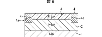
- FIG. 1B is a schematic cross-sectional view subsequent to FIG. 1A showing the method of manufacturing the compound semiconductor device according to the first embodiment in the order of steps.
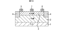
- FIG. 1C is a schematic cross-sectional view subsequent to FIG. 1B showing the method of manufacturing the compound semiconductor device according to the first embodiment in the order of steps.
- FIG. 1D is a schematic cross-sectional view illustrating the method of manufacturing the compound semiconductor device according to the first embodiment in the order of steps, following FIG. 1C.
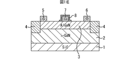
- FIG. 1E is a schematic cross-sectional view illustrating the method of manufacturing the compound semiconductor device according to the first embodiment in the order of steps, following FIG. 1D.
- FIG. 1F is a schematic cross-sectional view showing the method of manufacturing the compound semiconductor device according to the first embodiment in the order of steps, following FIG. 1E.
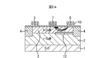
- FIG. 2A is a schematic cross-sectional view illustrating functions of a comparative example of the compound semiconductor device according to the first embodiment.
- FIG. 2B is a schematic cross-sectional view illustrating the function of the compound semiconductor device according to the first embodiment.
- FIG. 3A is a schematic cross-sectional view showing Modification 1 of the first embodiment.
- FIG. 3B is a schematic cross-sectional view showing Modification 2 of the first embodiment.
- FIG. 3C is a schematic cross-sectional view showing a third modification of the first embodiment.
- FIG. 1A is a schematic cross-sectional view illustrating functions of a comparative example of the compound semiconductor device according to the first embodiment.
- FIG. 2B is a schematic cross-sectional view illustrating the function of the compound semiconductor device according to the first embodiment.
- FIG. 3A is a schematic cross-
- FIG. 4A is a schematic cross-sectional view showing the method of manufacturing the compound semiconductor device according to the second embodiment in the order of steps.
- FIG. 4B is a schematic cross-sectional view illustrating the manufacturing method of the compound semiconductor device according to the second embodiment in the order of steps, following FIG. 4A.
- FIG. 4C is a schematic cross-sectional view illustrating the method of manufacturing the compound semiconductor device according to the second embodiment in the order of steps, following FIG. 4B.
- FIG. 4D is a schematic cross-sectional view subsequent to FIG. 4C, illustrating the method for manufacturing the compound semiconductor device according to the second embodiment in the order of steps.
- FIG. 4E is a schematic cross-sectional view illustrating the method of manufacturing the compound semiconductor device according to the second embodiment in the order of steps, following FIG. 4D.
- FIG. 4F is a schematic cross-sectional view illustrating the method of manufacturing the compound semiconductor device according to the second embodiment in the order of steps, following FIG. 4E.
- FIG. 4G is a schematic cross-sectional view showing the method of manufacturing the compound semiconductor device according to the second embodiment in the order of steps, following FIG. 4F.
- FIG. 5A is a schematic cross-sectional view showing the method of manufacturing the compound semiconductor device according to the third embodiment in the order of steps.
- FIG. 5B is a schematic cross-sectional view illustrating the manufacturing method of the compound semiconductor device according to the third embodiment in the order of steps, following FIG. 5A.
- FIG. 6A is a schematic cross-sectional view showing the method of manufacturing the compound semiconductor device according to the fourth embodiment in the order of steps.
- FIG. 6B is a schematic cross-sectional view illustrating the manufacturing method of the compound semiconductor device according to the fourth embodiment in the order of steps, following FIG. 6A.
- FIG. 6C is a schematic cross-sectional view illustrating the manufacturing method of the compound semiconductor device according to the fourth embodiment in the order of steps, following FIG. 6B.
- FIG. 6D is a schematic cross-sectional view subsequent to FIG. 6C, illustrating the method for manufacturing the compound semiconductor device according to the fourth embodiment in the order of steps.
- the electric field in the region between the drain electrode and the gate electrode (hereinafter referred to as “DG region”) is referred to in the DG region. What is necessary is just to disperse.
- attention is focused on the two-dimensional electron gas concentration at the interface between the electron transit layer and the electron supply layer of the compound semiconductor device, in other words, the sheet carrier concentration.
- the portion below the drain side gate bottom end is adjusted to a state in which the two-dimensional electron gas concentration is lower than the other portions. By doing so, the sheet resistance in the vicinity becomes higher than the other portions, and the electric field in the DG region is dispersed in the DG region.
- a protective film formed so as to cover the source electrode, the drain electrode, and the gate electrode is used for the purpose of reducing surface traps.
- two types of insulating films are formed in the DG region by changing the film formation conditions, for example, changing the hydrogen concentration or input power in the source gas.
- the portion corresponding to the vicinity of the drain side gate bottom end of the DG region may be subjected to electron beam irradiation or ion implantation to alter the crystalline state in the vicinity.
- an electron transit layer 2 and an electron supply layer 3 are formed.
- an intentionally undoped GaN (i-GaN) and an intentionally undoped AlGaN (i-AlGaN) are sequentially deposited on the substrate, here the SiC substrate 1, for example, by the MOVPE method, and the electron transit layer 2 and The electron supply layer 3 is formed.
- the electron transit layer 2 is formed to a thickness of about 3 ⁇ m
- the electron supply layer 3 is formed to a thickness of 20 nm as Al 0.25 Ga 0.75 N.
- an element isolation structure 4 is formed by an STI (Shallow Trench Isolation) method.
- STI Shallow Trench Isolation
- a silicon oxide is deposited on the electron supply layer 3 by an insulator, here a CVD method or the like so as to fill the isolation groove 4a.
- the silicon oxide on the electron supply layer 3 is polished and removed by a CMP (Chemical-Mechanical Polishing) method.
- the element isolation structure 4 filling the isolation groove 4a is formed.
- the remaining region on the electron supply layer 3 becomes an active region.
- impurities are ion-implanted into the element isolation region on the electron supply layer 3 to make the element isolation region in an insulating state. Also good.
- a source electrode 5, a drain electrode 6, and a gate electrode 7 are formed. More specifically, first, a resist is applied to the entire surface, and a resist pattern (not shown) having openings at portions where the source electrode 5 and the drain electrode 6 in the active region are to be formed is formed by lithography. Then, an electrode material, for example, Ti / Al is laminated on the resist pattern so as to fill the opening by, for example, vapor deposition. Thereafter, the resist pattern is removed together with Ti / Al thereon using a heated organic solvent or the like. Thereafter, the SiC substrate 1 is annealed at a temperature of about 550 ° C., for example. Thus, the source electrode 5 and the drain electrode 6 which are a pair of ohmic electrodes made of Ti / Al are formed.
- a resist is applied to the entire surface, and a resist pattern (not shown) having an opening at a site where the gate electrode 7 is to be formed is formed by lithography. Then, an electrode material, for example, Ni / Au is laminated on the resist pattern so as to fill the opening, for example, by vapor deposition. Thereafter, the resist pattern is removed together with Ni / Au thereon using a heated organic solvent or the like. Thus, the gate electrode 7 made of Ni / Au is formed.
- the protective films 8 and 9 are formed of, for example, a SiN film as an insulating film.
- the protective film 8 is formed, for example, at a hydrogen concentration higher than that of the protective film 9 so that the refractive index is higher than that of the protective film 9.
- the protective film 8 covers the gate electrode 7 and is formed on the electron supply layer 3 so as to extend to the vicinity of the gate electrode 7.
- the protective film 9 is formed on the entire surface so as to cover the protective film 8.
- a protective film 8 is formed on the entire surface so as to cover the gate electrode 7.
- a plasma CVD method is used.
- the protective film 8 is processed. Specifically, the protective film 8 is processed by lithography and dry etching using, for example, a fluorine-based gas, and the protective film 8 is left so as to cover the gate electrode 7 and extend to the vicinity of the gate electrode 7 on the electron supply layer 3. .
- the distance between the drain electrode 6 and the gate electrode 7 (DG distance) is, for example, about (1 ⁇ m) to (20 ⁇ m), and the length of the protective film 8 on the electron supply layer 3 (the electron supply layer of the protective film 8)
- the length of the portion extending on 3 is, for example, about (0.1 ⁇ m) to (2 ⁇ m).
- a protective film 9 is formed on the entire surface so as to cover the protective film 8.
- a plasma CVD method is used.
- the flow rate of SiH 4 is adjusted to be smaller than that when the protective film 8 is formed. In this way, SiN having a thickness of about 50 nm is deposited on the entire surface, and the protective film 9 is formed.
- the hydrogen concentration of the protective films 8 and 9 is The hydrogen concentration of the protective film 8> the hydrogen concentration of the protective film 9.
- the hydrogen concentration of the protective films 8 and 9 is appropriately selected so that the flow rate of SiH 4 at the time of formation thereof is within a range of, for example, about 2.0 sccm to 3 sccm so that the protective film 8 has a higher flow rate than the protective film 9. It is adjusted by.
- the protective film 8 may be adjusted so that the material is appropriately altered than the protective film 9.
- the protective film 8 has a higher input power than the protective film 9 under the film forming conditions when the protective films 8 and 9 are formed by the plasma CVD method.
- the degree of alteration of the protective films 8 and 9 is appropriately selected so that the high-frequency output, which is input power at the time of formation, is within a range of, for example, about 50 W to 200 W so that the protective film 8 has a higher high-frequency output than the protective film 9. To be adjusted.
- the protective films 8 and 9 are formed by appropriately adjusting the flow rate and input power of SiH 4 in the source gas.
- An example of selection of film forming conditions is shown in Table 1 below. Table 1 shows the sheet resistance when the sheet resistance between GD before deposition of the protective film is 1.
- SiN (C) is defined as a standard.
- SiN (B) is a gas film formed by plasma CVD using a plasma excitation frequency of 13.56 MHz, a high-frequency output of 50 W as input power, a source gas as a mixed gas of SiH 4 , N 2 , and He.
- SiN (C) is a gas film formed by plasma CVD using a plasma excitation frequency of 13.56 MHz, a high-frequency output of 100 W as input power, a source gas as a mixed gas of SiH 4 , N 2 , and He.
- This is a protective film formed at a flow rate of SiH 4 / N 2 /He 2.9 sccm / 150 sccm / 1000 sccm.
- SiN (D) is a gas deposition condition for plasma CVD, with a plasma excitation frequency of 13.56 MHz, a high-frequency output of 200 W as input power, a source gas as a mixed gas of SiH 4 , N 2 , and He.
- the protective film 8 has a higher sheet resistance than the protective film 9, and the protective films 8, 9 may be formed.
- an AlGaN / GaN • FET is formed.
- FIGS. 1A to 1E are schematic cross-sectional views illustrating the function of the compound semiconductor device.
- FIG. 2A shows a comparative example
- FIG. 2B shows this embodiment.
- the protective film 10 is formed to a thickness of about 100 nm under the standard conditions shown in Table 1 (conditions for forming SiN (C)).
- a two-dimensional electron gas exists at the interface between the electron transit layer 2 and the electron supply layer 3.
- the two-dimensional electron gas concentration (sheet carrier concentration) is substantially constant in the interface region 13 between DG.
- the sheet resistance immediately below the protective film 10 is substantially constant.
- the electric field generated between DG from the drain electrode 6 toward the gate electrode 7 is concentrated in the vicinity of the bottom end of the gate electrode 7 on the drain electrode 6 side, as indicated by the arrow in FIG. 2A. Due to this electric field concentration, the gate leakage current increases.
- the lower part of the protective film 8 is lower than the two-dimensional electron gas concentration of the first interface region 11 corresponding to the lower part of the protective film 9 between DG.
- the two-dimensional electron gas concentration in the second interface region 12 which is a portion corresponding to is lower. Therefore, the sheet resistance R2 immediately below the protective film 8 (the contact portion of the electron supply layer 3 with the protective film 8) is the sheet resistance R1 immediately below the protective film 9 (the contact portion of the electron supply layer 3 with the protective film 9). Higher than. R2> R1
- a highly reliable AlGaN / GaN FET that achieves high voltage operation, high withstand voltage, and high output is achieved by significantly reducing gate leakage with a relatively simple configuration. To do.
- 3A to 3C are schematic cross-sectional views showing only the state of the AlGaN / GaN FET corresponding to FIG. 1F of the first embodiment in various modifications of the first embodiment.
- 3A corresponds to the first modification
- FIG. 3B corresponds to the second modification
- FIG. 3C corresponds to the third modification.
- the gate electrode 7 is biased toward the source electrode 5 in the region between the source electrode 5 and the drain electrode 6 (between SG) on the electron supply layer 3. Is formed. In other words, the gate electrode 7 is formed at a position where the distance between SG is shorter than the distance between DG. In order to form the gate electrode 7 at the bias position as described above, after forming the source electrode 5 and the drain electrode 6 in the step of FIG. 1C in the first embodiment, the gate electrode 7 is formed at a desired bias position. Just do it.
- the distance between DG becomes longer, so that the electric field concentration at the bottom end of the gate electrode 7 on the drain electrode 6 side is further relaxed, Generation of gate leakage can be suppressed more reliably.
- the protective film 8 below the protective film 9 covers the gate electrode 7 from a predetermined portion on the upper surface of the gate electrode 7 toward the drain electrode 6, and the gate is formed on the electron supply layer 3. It is formed so as to extend to the vicinity of the electrode 7.
- the protective film 8 does not exist in the vicinity of the gate electrode 7 on the source electrode 5 side on the electron supply layer 3.
- a protective film 8 is not particularly required in the vicinity of the gate electrode 7 on the source electrode 5 side on the supply layer 3.
- the protective film 8 formed over the entire surface so as to cover the gate electrode 7 in the step of FIG. Processed by dry etching using a system gas. That is, the gate electrode 7 is covered from a predetermined portion on the upper surface of the gate electrode 7 toward the drain electrode 6, and the protective film 8 is left so as to extend to the vicinity of the gate electrode 7 on the electron supply layer 3.
- the protective film 8 is formed only in necessary portions as much as possible, thereby simplifying the configuration.
- Modification 3 In this example, as shown in FIG. 3C, an AlGaN / GaN.FET employing both of the first and second modifications is disclosed. That is, the gate electrode 7 is formed so as to be biased toward the source electrode 5 side rather than the drain electrode 6 side, and the protective film 8 is formed from a predetermined portion on the upper surface of the gate electrode 7 toward the drain electrode 6 side. And extends to the vicinity of the gate electrode 7 on the electron supply layer 3. According to this example, in addition to the various effects in the first embodiment described above, both the effects specific to the above-described modified examples 1 and 2 are exhibited.
- the same steps as in FIGS. 1A and 1B are performed. Subsequently, as shown in FIG. 4A, after forming the source electrode 5 and the drain electrode 6 as in FIG. 1C, as shown in FIG. 4B, the same film formation conditions as those of the protective film 8 formed in FIG. 1D. Thus, the protective film 8 is formed on the entire surface.
- the protective film 8 is processed. Specifically, the protective film 8 is processed by lithography and dry etching using, for example, a fluorine-based gas, and the protective film 8 is left in a portion where the gate electrode is to be formed so as to slightly protrude from the portion to at least the drain electrode 6 side. .
- the protective film 8 may be left in a shape protruding only on the drain electrode 6 side.
- the protective film 9 is formed on the entire surface so as to cover the protective film 8 under the same film formation conditions as those of the protective film 9 formed in FIG. 1F.
- openings 23 are formed in the protective films 8 and 9.
- the protective film 9 and the protective film 8 are processed by lithography and dry etching using, for example, a fluorine-based gas, thereby forming an opening 23 that exposes the formation site of the gate electrode on the surface of the electron supply layer 3.
- a fluorine-based gas for example, a fluorine-based gas
- the protective film 8 remains on the electron supply layer 3 so that one end surface is exposed from the inner wall of the opening 23 and extends slightly toward at least the drain electrode 6 side.
- the protective film 8 is left in a shape that protrudes only on the drain electrode 6 side in the step of FIG. 4C, the protective film 8 remains only on the drain electrode 6 side in the step of FIG. 4E.
- the resist pattern 21 may be formed of a two-layer resist. Specifically, first, a resist is applied to the entire surface so as to fill the opening 23, and the resist is exposed by lithography to process the resist. Specifically, an opening 21 a having a slightly larger size is formed at a portion corresponding to a portion where the gate electrode of the resist is to be formed at least on the drain electrode 6 side than the portion to form a resist pattern 21. Next, a gate material 22, for example, Ni / Au, for example, is deposited on the resist pattern 21 so as to fill the openings 21a and 23 by vapor deposition.
- the gate electrode 14 is formed. Specifically, the resist pattern 21 is removed together with the gate material 22 thereon using a heated organic solvent or the like. As described above, the gate electrode 14 made of Ni / Au having a bottom end in contact with one end face of the protective film 8 on the electron supply layer 3 and a so-called overhang shape in which the upper portion rides on the protective film 9 at the end. It is formed.
- the two-dimensional electron gas concentration in the first interface region 11 corresponding to the lower part of the protective film 9 between DG is the same as in the first embodiment.
- the two-dimensional electron gas concentration in the second interface region 12 corresponding to the portion below the protective film 8 is lower. Accordingly, the sheet resistance immediately below the protective film 8 (the contact portion of the electron supply layer 3 with the protective film 8) is higher than the sheet resistance immediately below the protective film 9 (the contact portion of the electron supply layer 3 with the protective film 9). high.
- the electric field concentration at the bottom end of the gate electrode 14 on the drain electrode 6 side is alleviated, the gate leakage current is greatly reduced, and the gate breakdown voltage is improved. Furthermore, in the present embodiment, the gate electrode 14 has a shape that rides on the protective film 9 with its upper portion at the end. Since there are two bottom ends on the drain electrode 6 side of the gate electrode 14, the electric field generated between DG from the drain electrode 6 toward the gate electrode 7 is dispersed to the two bottom ends. . Therefore, due to the shape of the gate electrode 14, the electric field concentration at the bottom end of the gate electrode 14 on the drain electrode 6 side is further relaxed.
- the gate electrode 14 may be formed so as to be biased toward the source electrode 5 rather than the drain electrode 6 as in the first modification of the first embodiment.
- a highly reliable AlGaN / GaN FET that achieves high voltage operation, high withstand voltage, and high output is achieved by significantly reducing gate leakage with a relatively simple configuration. To do.
- an electron beam is irradiated to both sides of the site where the gate electrode of the electron supply layer 3 is to be formed.
- the electron beam may be irradiated only on the side of the drain electrode 6 where the gate electrode is to be formed.
- the electron beam irradiation conditions are, for example, 20 keV and 1000 ⁇ C / cm 2 .
- a predetermined element for example, Ar is ion-implanted only on both sides of the gate electrode formation scheduled portion of the electron supply layer 3 or on the drain electrode 6 side so as to form a depletion region. Also good.
- the gate electrode 7 is formed so as to be in contact with (or close to) the depletion region 31 at the bottom end under the same conditions as in FIG. 1C of the first embodiment.
- a protective film 9 is formed (the protective film 8 is not formed) to form an AlGaN / GaN • FET.
- the two-dimensional electron gas concentration in the first interface region 11 which is a portion corresponding to the lower part of the protective film 9 where the depletion region 31 is not formed is formed.
- the two-dimensional electron gas concentration in the second interface region 12 corresponding to the portion below the depletion region 31 is lower. Therefore, the sheet resistance in the depletion region 31 is higher than the sheet resistance immediately below the protective film 9 (the contact portion of the electron supply layer 3 with the protective film 9).
- the electric field concentration at the bottom end of the gate electrode 7 on the drain electrode 6 side is alleviated, the gate leakage current is greatly reduced, and the gate breakdown voltage is improved.
- a highly reliable AlGaN / GaN FET that achieves high voltage operation, high withstand voltage, and high output is achieved by significantly reducing gate leakage with a relatively simple configuration. To do.
- n-Gan.FET having an n-type GaN (n-Gan) layer on an electron supply layer
- 6A to 6D are schematic cross-sectional views sequentially showing main processes of the compound semiconductor device manufacturing method according to the fourth embodiment.
- the cap layer 41 is formed. Specifically, on the electron supply layer 3, for example, by MOVPE method, n-Gan (for example, Si is doped and the doping concentration is about 2 ⁇ 10 18 / cm 3 ) is 10 nm or less, for example, about 5 nm. To form a cap layer 41. By forming the cap layer 41, surface traps can be further reduced.
- n-Gan for example, Si is doped and the doping concentration is about 2 ⁇ 10 18 / cm 3
- an opening 42 is formed at a site where the source electrode and the drain electrode are to be formed. More specifically, the depth at which a part of the electron supply layer 3 under the cap layer 41 is dug in the site where the source and drain electrodes are to be formed on the cap layer 41 by lithography and dry etching using a chlorine-based gas or the like. The opening 42 is formed.
- a source electrode 43 and a drain electrode 44 are formed. More specifically, a resist is applied to the entire surface, and a resist pattern (not shown) having an opening that exposes the opening 42 that is a site where the source electrode 5 and the drain electrode 6 in the active region are to be formed is formed by lithography. Then, an electrode material, for example, Ti / Al is laminated on the resist pattern so as to fill the opening by, for example, vapor deposition. Thereafter, the resist pattern is removed together with Ti / Al thereon using a heated organic solvent or the like. Thereafter, the SiC substrate 1 is annealed at a temperature of about 550 ° C., for example. As a result, the source electrode 43 and the drain electrode 44, which are a pair of ohmic electrodes, in which the opening 42 is filled with Ti / Al and the upper portion protrudes from the surface of the cap layer 41 are formed.
- a resist pattern (not shown) having an opening that exposes the opening 42 that is a site where the source electrode 5
- the gate electrode 7 is formed on the cap layer 41 under the same conditions as in FIG. 1C of the first embodiment, and the protective films 8 and 9 are formed as in FIGS. 1D to 1F.
- an AlGaN / GaN • FET is formed.
- the two-dimensional electron gas concentration in the first interface region 11 corresponding to the lower part of the protective film 9 between DG is the same as in the first embodiment.
- the two-dimensional electron gas concentration in the second interface region 12 corresponding to the portion below the protective film 8 is lower. Accordingly, the sheet resistance immediately below the protective film 8 (the contact portion of the electron supply layer 3 with the protective film 8) is higher than the sheet resistance immediately below the protective film 9 (the contact portion of the electron supply layer 3 with the protective film 9). high.
- the gate electrode 7 may be formed so as to be biased toward the source electrode 5 side rather than the drain electrode 6 side, as in the first modification of the first embodiment.
- the protective film 8 covers the gate electrode 7 from a predetermined portion on the upper surface of the gate electrode 7 toward the drain electrode 6, and the gate electrode is formed on the electron supply layer 3. You may form so that it may extend to 7 vicinity.
- the gate electrode 7 is formed so as to be biased toward the source electrode 5 side rather than the drain electrode 6 side, and the protective film 8 is formed on the upper surface of the gate electrode 7.
- the gate electrode 7 may be covered from the predetermined portion toward the drain electrode 6 and may be formed to extend to the vicinity of the gate electrode 7 on the electron supply layer 3.
- the protective film 8 may be formed so that the protective film 8 exists only on the cap layer 41 and contacts the bottom end of the gate electrode 7.
- the both sides (or only the drain electrode 6 side) of the portion of the cap layer 41 where the gate electrode is to be formed are irradiated (or the element is ionized). A depletion region may be formed.
- a highly reliable AlGaN / GaN FET that achieves high voltage operation, high withstand voltage, and high output is achieved by significantly reducing gate leakage with a relatively simple configuration. To do.
- the SiN film is exemplified as the protective films 8 and 9, but other insulating films such as SiO 2 and Al 2 O 3 are protected. It may be used as a film. In this case, it is conceivable that the protective films 8 and 9 are formed not only from the same material but also from different materials.
- a highly reliable compound semiconductor device that achieves high voltage operation, high withstand voltage, and high output is realized by significantly reducing gate leakage with a relatively simple configuration.
Landscapes
- Junction Field-Effect Transistors (AREA)
- Physics & Mathematics (AREA)
- High Energy & Nuclear Physics (AREA)
- Formation Of Insulating Films (AREA)
- Engineering & Computer Science (AREA)
- Plasma & Fusion (AREA)
Abstract
2層の保護膜(8,9)を、保護膜(8)の直下部分が保護膜(9)の直下部分よりもシート抵抗が高くなるように形成する。保護膜(8,9)は、絶縁膜として例えばSiN膜により形成される。保護膜(8)は、保護膜(9)よりも屈折率が高くなるように、例えば保護膜(9)よりも高い水素濃度に形成される。保護膜(8)は、ゲート電極(7)を覆い電子供給層(3)上でゲート電極(7)の近傍まで延在するように形成される。保護膜(9)は、保護膜(8)を覆うように全面に形成される。この構成により、比較的簡易な構成でゲートリークを大幅に低減し、高電圧動作、高耐圧及び高出力を達成する信頼性の高い化合物半導体装置が実現する。
Description
本発明は、窒化物半導体からなる電子走行層及び電子供給層を備えた化合物半導体装置及びその製造方法に関する。
近年、AlGaN/GaNのヘテロ接合を利用し、GaNを電子走行層とする化合物半導体装置であるAlGaN/GaN・FETの開発が活発である(例えば、特許文献1~4を参照)。GaNは、ワイドバンドギャップ、高い破壊電界強度、及び大きい飽和電子速度を有する材料であることから、高電圧動作且つ高出力を得る半導体装置の材料として極めて有望である。AlGaN/GaN・FETでは、AlGaNからなる電子供給層上にソース電極、ドレイン電極及びゲート電極が形成され、表面トラップを低減するための保護膜(例えばSiN膜)が全面に形成される。
しかしながら、上記のAlGaN/GaN・FETでは、想定されるよりも大きなゲートリークが発生することが多く、AlGaN/GaN・FETの利点として考えられている高電圧動作を行うことが困難となる。そのため、AlGaN/GaN・FETでは、ゲートリーク電流を低減する工夫が必須であるが、そのための有効な方策は採られていない現況にある。
本発明は、上記の課題に鑑みてなされたものであり、比較的簡易な構成でゲートリークを大幅に低減し、高電圧動作、高耐圧及び高出力を達成する信頼性の高い化合物半導体装置及びその製造方法を提供することを目的とする。
化合物半導体装置の一態様は、基板と、前記基板上方に形成された電子走行層と、前記電子走行層上方に形成された電子供給層と、前記電子供給層上方に形成された、ソース電極、ドレイン電極、及び前記ソース電極と前記ドレイン電極との間に形成されたゲート電極とを含み、前記電子走行層と前記電子供給層との間には、前記ゲート電極と前記ドレイン電極との間において、第1の領域と、前記第1の領域よりも2次元電子ガス濃度の低い第2の領域とが形成されており、前記第1の領域は前記ドレイン電極に偏倚する位置に、前記第2の領域は前記ゲート電極に偏倚する位置にそれぞれ形成されている。
化合物半導体装置の製造方法の一態様は、基板と、前記基板上方に形成された電子走行層と、前記電子走行層上方に形成された電子供給層と、前記電子供給層上方に形成された、ソース電極、ドレイン電極、及び前記ソース電極と前記ドレイン電極との間に形成されたゲート電極とを含む化合物半導体装置の製造方法であって、前記ゲート電極と前記ドレイン電極との間に、前記ゲート電極よりも前記ドレイン電極に近い位置に第1の絶縁膜を、前記ドレイン電極よりも前記ゲート電極に近い位置に第2の絶縁膜をそれぞれ形成し、前記電子走行層と前記電子供給層との間において、前記第2の絶縁膜の下方に相当する部分の2次元電子ガス濃度を、前記第1の絶縁膜の下方に相当する部分の2次元電子ガス濃度よりも低くする。
化合物半導体装置の製造方法の他態様は、基板と、前記基板上方に形成された電子走行層と、前記電子走行層上方に形成された電子供給層と、前記電子供給層上方に形成された、ソース電極、ドレイン電極、及び前記ソース電極と前記ドレイン電極との間に形成されたゲート電極とを含む化合物半導体装置の製造方法であって、前記電子供給層の表層に結晶状態を変質させた空乏領域を形成する工程と、前記空乏領域が前記ドレイン電極よりも前記ゲート電極に偏倚する部位に位置するように、前記ゲート電極を形成する工程とを含む。
上記の各態様によれば、比較的簡易な構成でゲートリークを大幅に低減し、高電圧動作、高耐圧及び高出力を達成する信頼性の高い化合物半導体装置が実現する。
―本実施形態の基本骨子―
化合物半導体装置において、ゲートリーク電流の増加は、高電圧印加時にドレイン電極からゲート電極への電界が、ゲート電極の底部のドレイン電極側の端部位(以下、「ドレイン側ゲート底部端」とする。)に集中することに起因して生じる。そこで、ゲートリーク電流を減少するには、ドレイン側ゲート底部端における電界集中を緩和することが重要である。
化合物半導体装置において、ゲートリーク電流の増加は、高電圧印加時にドレイン電極からゲート電極への電界が、ゲート電極の底部のドレイン電極側の端部位(以下、「ドレイン側ゲート底部端」とする。)に集中することに起因して生じる。そこで、ゲートリーク電流を減少するには、ドレイン側ゲート底部端における電界集中を緩和することが重要である。
ドレイン側ゲート底部端における電界集中を緩和するには、ドレイン電極とゲート電極との間の領域(以下、「D-G間領域」とする。)における電界を、D-G間領域内で言わば分散させれば良い。本実施形態では、化合物半導体装置の電子走行層と電子供給層との界面における2次元電子ガス濃度、換言すればシートキャリア濃度に着目する。D-G間領域の下方の前記界面において、ドレイン側ゲート底部端の近傍下の部分を、その他の部分よりも2次元電子ガス濃度が低い状態に調節する。このようにすることにより、当該近傍のシート抵抗がその他の部分よりも高くなり、D-G間領域における電界が、D-G間領域内で分散される。
上記のようにD-G間領域の2次元電子ガス濃度を調節すべく、表面トラップを低減させる目的でソース電極、ドレイン電極及びゲート電極を覆うように形成される保護膜を利用する。具体的には、成膜条件を変えて、例えばソースガス中の水素濃度又は投入電力を変えて、D-G間領域に2種類の絶縁膜を形成する。また、D-G間領域のドレイン側ゲート底部端の近傍に相当する部分に電子線照射又はイオン注入等を行い、当該近傍の結晶状態を変質させるようにしても良い。
このように、D-G間領域の2次元電子ガス濃度を調節することにより、ドレイン側ゲート底部端における電界集中が大幅に緩和され、ゲートリークが低減し、化合物半導体装置の高電圧動作、高耐圧及び高出力を得ることができる。
このように、D-G間領域の2次元電子ガス濃度を調節することにより、ドレイン側ゲート底部端における電界集中が大幅に緩和され、ゲートリークが低減し、化合物半導体装置の高電圧動作、高耐圧及び高出力を得ることができる。
―具体的な実施形態―
以下、上記の基本骨子を踏まえ、具体的な諸実施形態について図面を参照して詳細に説明する。
以下、上記の基本骨子を踏まえ、具体的な諸実施形態について図面を参照して詳細に説明する。
(第1の実施形態)
本実施形態では、化合物半導体装置であるAlGaN/GaN・FETの構成について、その製造方法と共に説明する。
図1A~図1Fは、第1の実施形態による化合物半導体装置の製造方法を工程順に示す概略断面図である。
本実施形態では、化合物半導体装置であるAlGaN/GaN・FETの構成について、その製造方法と共に説明する。
図1A~図1Fは、第1の実施形態による化合物半導体装置の製造方法を工程順に示す概略断面図である。
先ず、図1Aに示すように、電子走行層2及び電子供給層3を形成する。
詳細には、基板、ここではSiC基板1上に、例えばMOVPE法により、インテンショナリーアンドープGaN(i-GaN)及びインテンショナリーアンドープAlGaN(i-AlGaN)を順次堆積し、電子走行層2及び電子供給層3を形成する。ここで、電子走行層2は膜厚3μm程度、電子供給層3はAl0.25Ga0.75Nとして膜厚20nmに形成する。
詳細には、基板、ここではSiC基板1上に、例えばMOVPE法により、インテンショナリーアンドープGaN(i-GaN)及びインテンショナリーアンドープAlGaN(i-AlGaN)を順次堆積し、電子走行層2及び電子供給層3を形成する。ここで、電子走行層2は膜厚3μm程度、電子供給層3はAl0.25Ga0.75Nとして膜厚20nmに形成する。
続いて、図1Bに示すように、STI(Shallow Trench Isolation)法により素子分離構造4を形成する。
詳細には、先ず、リソグラフィー及び塩素系ガス等を用いたドライエッチングにより、電子供給層3上の素子分離領域に、電子供給層3下の電子走行層2の一部を掘り込む深さの分離溝4aを形成する。
詳細には、先ず、リソグラフィー及び塩素系ガス等を用いたドライエッチングにより、電子供給層3上の素子分離領域に、電子供給層3下の電子走行層2の一部を掘り込む深さの分離溝4aを形成する。
次に、分離溝4a内を埋め込むように絶縁物、ここではCVD法等により電子供給層3上にシリコン酸化物を堆積する。そして、例えばCMP(Chemical-Mechanical Polishing)法により電子供給層3上のシリコン酸化物を研磨して除去する。このとき、分離溝4a内を充填する素子分離構造4が形成される。素子分離構造4の形成により、残存する電子供給層3上の領域が活性領域となる。
ここで、分離溝4aを形成して分離溝4aに絶縁物を充填する代わりに、電子供給層3上の素子分離領域に不純物をイオン注入し、素子分離領域を絶縁状態にする手法を用いても良い。
ここで、分離溝4aを形成して分離溝4aに絶縁物を充填する代わりに、電子供給層3上の素子分離領域に不純物をイオン注入し、素子分離領域を絶縁状態にする手法を用いても良い。
続いて、図1Cに示すように、ソース電極5、ドレイン電極6、及びゲート電極7が形成される。
詳細には、先ず、全面にレジストを塗布し、リソグラフィーにより、活性領域のソース電極5及びドレイン電極6の形成予定部位に開口を有するレジストパターン(不図示)を形成する。そして、例えば蒸着法により電極材料、例えばTi/Alを開口を埋め込むようにレジストパターン上に積層する。その後、加温した有機溶媒等を用いてレジストパターンをその上のTi/Alと共に除去する。その後、例えば550℃程度の温度によりSiC基板1にアニール処理を施す。以上により、Ti/Alからなる一対のオーミック電極であるソース電極5及びドレイン電極6が形成される。
詳細には、先ず、全面にレジストを塗布し、リソグラフィーにより、活性領域のソース電極5及びドレイン電極6の形成予定部位に開口を有するレジストパターン(不図示)を形成する。そして、例えば蒸着法により電極材料、例えばTi/Alを開口を埋め込むようにレジストパターン上に積層する。その後、加温した有機溶媒等を用いてレジストパターンをその上のTi/Alと共に除去する。その後、例えば550℃程度の温度によりSiC基板1にアニール処理を施す。以上により、Ti/Alからなる一対のオーミック電極であるソース電極5及びドレイン電極6が形成される。
次に、全面にレジストを塗布し、リソグラフィーにより、ゲート電極7の形成予定部位に開口を有するレジストパターン(不図示)を形成する。そして、例えば蒸着法により電極材料、例えばNi/Auを開口を埋め込むようにレジストパターン上に積層する。その後、加温した有機溶媒等を用いてレジストパターンをその上のNi/Auと共に除去する。以上により、Ni/Auからなるゲート電極7が形成される。
続いて、図1D~図1Fに示すように、2層の保護膜8,9を、保護膜8の直下部分が保護膜9の直下部分よりもシート抵抗が高くなるように形成する。保護膜8,9は、絶縁膜として例えばSiN膜により形成される。保護膜8は、保護膜9よりも屈折率が高くなるように、例えば保護膜9よりも高い水素濃度に形成される。保護膜8は、ゲート電極7を覆い電子供給層3上でゲート電極7の近傍まで延在するように形成される。保護膜9は、保護膜8を覆うように全面に形成される。
以下、図1D~図1Fの各工程を詳述する。
以下、図1D~図1Fの各工程を詳述する。
先ず、図1Dに示すように、ゲート電極7を覆うように全面に保護膜8を形成する。
詳細には、例えばプラズマCVD法を用いる。成膜条件は、プラズマの励起周波数を13.56MHz、投入電力である高周波出力を50W、ソースガスをSiH4、N2、及びHeの混合ガスとして、ガス流量をSiH4/N2/He=3sccm/150sccm/1000sccmとする。このようにして、膜厚50nm程度のSiNを全面に堆積し、保護膜8を形成する。
詳細には、例えばプラズマCVD法を用いる。成膜条件は、プラズマの励起周波数を13.56MHz、投入電力である高周波出力を50W、ソースガスをSiH4、N2、及びHeの混合ガスとして、ガス流量をSiH4/N2/He=3sccm/150sccm/1000sccmとする。このようにして、膜厚50nm程度のSiNを全面に堆積し、保護膜8を形成する。
続いて、図1Eに示すように、保護膜8を加工する。
詳細には、リソグラフィー及び例えばフッ素系ガスを用いたドライエッチングにより保護膜8を加工し、ゲート電極7を覆い電子供給層3上でゲート電極7の近傍まで延在するように保護膜8を残す。ドレイン電極6とゲート電極7との距離(D-G間距離)は例えば(1μm)~(20μm)程度であり、保護膜8の電子供給層3上における長さ(保護膜8の電子供給層3上で延在する部分の長さ)は、例えば(0.1μm)~(2μm)程度とされる。
詳細には、リソグラフィー及び例えばフッ素系ガスを用いたドライエッチングにより保護膜8を加工し、ゲート電極7を覆い電子供給層3上でゲート電極7の近傍まで延在するように保護膜8を残す。ドレイン電極6とゲート電極7との距離(D-G間距離)は例えば(1μm)~(20μm)程度であり、保護膜8の電子供給層3上における長さ(保護膜8の電子供給層3上で延在する部分の長さ)は、例えば(0.1μm)~(2μm)程度とされる。
続いて、図1Fに示すように、保護膜8を覆うように全面に保護膜9を形成する。
詳細には、例えばプラズマCVD法を用いる。成膜条件は、プラズマの励起周波数を13.56MHz、投入電力である高周波出力を50W、ソースガスをSiH4、N2、及びHeの混合ガスとして、ガス流量をSiH4/N2/He=2sccm/150sccm/1000sccmとする。ここでは、SiH4の流量を保護膜8の形成時よりも小さく調節する。このようにして、膜厚50nm程度のSiNを全面に堆積し、保護膜9を形成する。
詳細には、例えばプラズマCVD法を用いる。成膜条件は、プラズマの励起周波数を13.56MHz、投入電力である高周波出力を50W、ソースガスをSiH4、N2、及びHeの混合ガスとして、ガス流量をSiH4/N2/He=2sccm/150sccm/1000sccmとする。ここでは、SiH4の流量を保護膜8の形成時よりも小さく調節する。このようにして、膜厚50nm程度のSiNを全面に堆積し、保護膜9を形成する。
上記のようにSiH4の流量を調節することにより、保護膜8,9の水素濃度は、
保護膜8の水素濃度>保護膜9の水素濃度
となる。
保護膜8,9の水素濃度は、その形成時のSiH4の流量を例えば2.0sccm程度~3sccm程度の範囲内で保護膜8が保護膜9よりも流量が大きくなるように適宜選択することにより、調整される。
保護膜8の水素濃度>保護膜9の水素濃度
となる。
保護膜8,9の水素濃度は、その形成時のSiH4の流量を例えば2.0sccm程度~3sccm程度の範囲内で保護膜8が保護膜9よりも流量が大きくなるように適宜選択することにより、調整される。
保護膜8,9を形成するに際して、上記のように水素濃度を調節する代わりに、保護膜8を保護膜9よりも材質が適度に変質するように調節しても良い。具体的には、保護膜8,9のプラズマCVD法による形成時の成膜条件において、保護膜8を保護膜9よりも高い投入電力とする。
保護膜8,9の変質度合いは、その形成時の投入電力である高周波出力を例えば50W程度~200W程度の範囲内で保護膜8が保護膜9よりも高周波出力が大きくなるように適宜選択することにより、調整される。
保護膜8,9の変質度合いは、その形成時の投入電力である高周波出力を例えば50W程度~200W程度の範囲内で保護膜8が保護膜9よりも高周波出力が大きくなるように適宜選択することにより、調整される。
保護膜8,9は、ソースガス中のSiH4の流量及び投入電力を適宜調節して形成される。成膜条件の選択の一例を以下の表1に示す。表1では、保護膜堆積前のG-D間のシート抵抗を1とした場合のシート抵抗を表している。ここでは、SiN(C)を標準と規定する。

SiN(A)は、プラズマCVD法の成膜条件を、プラズマの励起周波数を13.56MHz、投入電力である高周波出力を50W、ソースガスをSiH4、N2、及びHeの混合ガスとして、ガス流量をSiH4/N2/He=2.0sccm/150sccm/1000sccmとして形成した保護膜である。
SiN(B)は、プラズマCVD法の成膜条件を、プラズマの励起周波数を13.56MHz、投入電力である高周波出力を50W、ソースガスをSiH4、N2、及びHeの混合ガスとして、ガス流量をSiH4/N2/He=2.9sccm/150sccm/1000sccmとして形成した保護膜である。
SiN(C)は、プラズマCVD法の成膜条件を、プラズマの励起周波数を13.56MHz、投入電力である高周波出力を100W、ソースガスをSiH4、N2、及びHeの混合ガスとして、ガス流量をSiH4/N2/He=2.9sccm/150sccm/1000sccmとして形成した保護膜である。
SiN(D)は、プラズマCVD法の成膜条件を、プラズマの励起周波数を13.56MHz、投入電力である高周波出力を200W、ソースガスをSiH4、N2、及びHeの混合ガスとして、ガス流量をSiH4/N2/He=3.0sccm/150sccm/1000sccmとして形成した保護膜である。
SiN(B)は、プラズマCVD法の成膜条件を、プラズマの励起周波数を13.56MHz、投入電力である高周波出力を50W、ソースガスをSiH4、N2、及びHeの混合ガスとして、ガス流量をSiH4/N2/He=2.9sccm/150sccm/1000sccmとして形成した保護膜である。
SiN(C)は、プラズマCVD法の成膜条件を、プラズマの励起周波数を13.56MHz、投入電力である高周波出力を100W、ソースガスをSiH4、N2、及びHeの混合ガスとして、ガス流量をSiH4/N2/He=2.9sccm/150sccm/1000sccmとして形成した保護膜である。
SiN(D)は、プラズマCVD法の成膜条件を、プラズマの励起周波数を13.56MHz、投入電力である高周波出力を200W、ソースガスをSiH4、N2、及びHeの混合ガスとして、ガス流量をSiH4/N2/He=3.0sccm/150sccm/1000sccmとして形成した保護膜である。
例えば、SiN(A)~(D)の成膜条件のうちから、保護膜8が保護膜9よりも高いシート抵抗となるように、適宜に2つの成膜条件を選択し、保護膜8,9を形成すれば良い。
以上のようにして、AlGaN/GaN・FETを形成する。
以上のようにして、AlGaN/GaN・FETを形成する。
以下、本実施形態による化合半導体装置の機能を、保護膜が単層である比較例との比較に基づいて説明する。
図2A及び図2Bは、化合半導体装置の機能を説明する概略断面図であり、図2Aが比較例を、図2Bが本実施形態をそれぞれ示す。図2Aの比較例では、図1A~図1Eの各工程を経た後、例えば表1の標準条件(SiN(C)を成膜する条件)で膜厚100nm程度に保護膜10が形成される。
図2A及び図2Bは、化合半導体装置の機能を説明する概略断面図であり、図2Aが比較例を、図2Bが本実施形態をそれぞれ示す。図2Aの比較例では、図1A~図1Eの各工程を経た後、例えば表1の標準条件(SiN(C)を成膜する条件)で膜厚100nm程度に保護膜10が形成される。
化合半導体装置では、電子走行層2と電子供給層3との界面に2次元電子ガスが存在する。当該界面のうち、D-G間の界面領域に着目する。
図2Aの比較例では、D-G間の界面領域13では、2次元電子ガス濃度(シートキャリア濃度)はほぼ一定である。従って、保護膜10の直下(電子供給層3の保護膜10との接触部分)におけるシート抵抗はほぼ一定である。この構成により、ドレイン電極6からゲート電極7へ向かってD-G間に発生する電界は、図2Aの矢印で示すように、ゲート電極7のドレイン電極6側の底部端の近傍に集中する。この電界集中に起因して、ゲートリーク電流が増加する。
図2Aの比較例では、D-G間の界面領域13では、2次元電子ガス濃度(シートキャリア濃度)はほぼ一定である。従って、保護膜10の直下(電子供給層3の保護膜10との接触部分)におけるシート抵抗はほぼ一定である。この構成により、ドレイン電極6からゲート電極7へ向かってD-G間に発生する電界は、図2Aの矢印で示すように、ゲート電極7のドレイン電極6側の底部端の近傍に集中する。この電界集中に起因して、ゲートリーク電流が増加する。
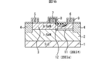
これに対して、図2Bの本実施形態では、D-G間では、保護膜9の下方に相当する部分である第1の界面領域11の2次元電子ガス濃度よりも、保護膜8の下方に相当する部分である第2の界面領域12の2次元電子ガス濃度の方が低くなる。従って、保護膜8の直下(電子供給層3の保護膜8との接触部分)におけるシート抵抗R2は、保護膜9の直下(電子供給層3の保護膜9との接触部分)におけるシート抵抗R1よりも高い。
R2>R1
R2>R1
このシート抵抗の変化は、保護膜9の堆積時においてSiN膜の堆積中にSiがSiN膜の下方へ取り込まれ、電子供給層3の表面のポテンシャルが変化するために生じるものと考えられる。図2Bの構成により、ドレイン電極6からゲート電極7へ向かってD-G間に発生する電界は、図2Bの矢印で示すように、D-G間領域内で言わば分散する。
このように本実施形態では、ゲート電極7のドレイン電極6側の底部端における電界集中が緩和され、ゲートリーク電流が大幅に減少し、ゲート耐圧が改善される。
このように本実施形態では、ゲート電極7のドレイン電極6側の底部端における電界集中が緩和され、ゲートリーク電流が大幅に減少し、ゲート耐圧が改善される。
以上説明したように、本実施形態によれば、比較的簡易な構成でゲートリークを大幅に低減し、高電圧動作、高耐圧及び高出力を達成する信頼性の高いAlGaN/GaN・FETが実現する。
(変形例)
ここで、第1の実施形態の諸変形例について説明する。
図3A~図3Cは、第1の実施形態の諸変形例において、第1の実施形態の図1Fに相当するAlGaN/GaN・FETの様子のみを示す概略断面図である。図3Aが変形例1、図3Bが変形例2、図3Cが変形例3にそれぞれ対応している。
ここで、第1の実施形態の諸変形例について説明する。
図3A~図3Cは、第1の実施形態の諸変形例において、第1の実施形態の図1Fに相当するAlGaN/GaN・FETの様子のみを示す概略断面図である。図3Aが変形例1、図3Bが変形例2、図3Cが変形例3にそれぞれ対応している。
(1)変形例1
本例では、図3Aに示すように、電子供給層3上のソース電極5とドレイン電極6との間(S-G間)の領域において、ゲート電極7がソース電極5側に偏倚するように形成されている。換言すれば、S-G間の距離が、D-G間の距離よりも短くなる位置に、ゲート電極7が形成されている。
ゲート電極7を上記のような偏倚位置に形成するには、第1の実施形態における図1Cの工程において、ソース電極5及びドレイン電極6を形成した後に、ゲート電極7を所望の偏倚位置に形成すれば良い。
本例では、図3Aに示すように、電子供給層3上のソース電極5とドレイン電極6との間(S-G間)の領域において、ゲート電極7がソース電極5側に偏倚するように形成されている。換言すれば、S-G間の距離が、D-G間の距離よりも短くなる位置に、ゲート電極7が形成されている。
ゲート電極7を上記のような偏倚位置に形成するには、第1の実施形態における図1Cの工程において、ソース電極5及びドレイン電極6を形成した後に、ゲート電極7を所望の偏倚位置に形成すれば良い。
本例によれば、上記した第1の実施形態における諸効果に加えて、D-G間の距離が長くなるため、ゲート電極7のドレイン電極6側の底部端における電界集中が更に緩和され、ゲートリークの発生をより確実に抑えることができる。
(2)変形例2
本例では、図3Bに示すように、保護膜9下の保護膜8が、ゲート電極7の上面の所定部位からドレイン電極6側へ向かってゲート電極7を覆い、電子供給層3上でゲート電極7の近傍まで延在するように形成されている。電子供給層3上でソース電極5側におけるゲート電極7の近傍には、保護膜8は存在しない。
ドレイン電極6とゲート電極7との間における電界集中を緩和するには、保護膜8が、電子供給層3上でドレイン電極6側におけるゲート電極7の近傍に存在すれば十分であって、電子供給層3上でソース電極5側におけるゲート電極7の近傍には、保護膜8は特に要しない。
本例では、図3Bに示すように、保護膜9下の保護膜8が、ゲート電極7の上面の所定部位からドレイン電極6側へ向かってゲート電極7を覆い、電子供給層3上でゲート電極7の近傍まで延在するように形成されている。電子供給層3上でソース電極5側におけるゲート電極7の近傍には、保護膜8は存在しない。
ドレイン電極6とゲート電極7との間における電界集中を緩和するには、保護膜8が、電子供給層3上でドレイン電極6側におけるゲート電極7の近傍に存在すれば十分であって、電子供給層3上でソース電極5側におけるゲート電極7の近傍には、保護膜8は特に要しない。
保護膜8を本例のように形成するには、第1の実施形態における図1Eの工程において、ゲート電極7を覆うように全面形成された保護膜8を、以下のようにリソグラフィー及び例えばフッ素系ガスを用いたドライエッチングにより加工する。即ち、ゲート電極7の上面の所定部位からドレイン電極6側へ向かってゲート電極7を覆い、電子供給層3上でゲート電極7の近傍まで延在するように保護膜8を残す。
本例によれば、上記した第1の実施形態における諸効果に加えて、保護膜8をできるだけ必要な箇所にのみ形成し、構成の簡略化が図られる。
(3)変形例3
本例では、図3Cに示すように、変形例1,2を共に採用したAlGaN/GaN・FETを開示する。即ち、ゲート電極7がドレイン電極6側よりもソース電極5側に偏倚するように形成されると共に、保護膜8が、ゲート電極7の上面の所定部位からドレイン電極6側へ向かってゲート電極7を覆い、電子供給層3上でゲート電極7の近傍まで延在するように形成される。
本例によれば、上記した第1の実施形態における諸効果に加えて、上記した変形例1,2に特有の効果を共に奏する。
本例では、図3Cに示すように、変形例1,2を共に採用したAlGaN/GaN・FETを開示する。即ち、ゲート電極7がドレイン電極6側よりもソース電極5側に偏倚するように形成されると共に、保護膜8が、ゲート電極7の上面の所定部位からドレイン電極6側へ向かってゲート電極7を覆い、電子供給層3上でゲート電極7の近傍まで延在するように形成される。
本例によれば、上記した第1の実施形態における諸効果に加えて、上記した変形例1,2に特有の効果を共に奏する。
(第2の実施形態)
本実施形態では、化合物半導体装置であるAlGaN/GaN・FETの構成について、その製造方法と共に説明する。第1の実施形態とは、保護膜8の形成工程が異なる点で相違する。
図4A~図4Gは、第2の実施形態による化合物半導体装置の製造方法の主要工程を順に示す概略断面図である。
本実施形態では、化合物半導体装置であるAlGaN/GaN・FETの構成について、その製造方法と共に説明する。第1の実施形態とは、保護膜8の形成工程が異なる点で相違する。
図4A~図4Gは、第2の実施形態による化合物半導体装置の製造方法の主要工程を順に示す概略断面図である。
先ず、第1の実施形態と同様に、図1A及び図1Bと同様の各工程を経る。
続いて、図4Aに示すように、図1Cと同様に、ソース電極5及びドレイン電極6を形成した後、図4Bに示すように、図1Dで形成される保護膜8と同様の成膜条件により、全面に保護膜8を形成する。
続いて、図4Aに示すように、図1Cと同様に、ソース電極5及びドレイン電極6を形成した後、図4Bに示すように、図1Dで形成される保護膜8と同様の成膜条件により、全面に保護膜8を形成する。
続いて、図4Cに示すように、保護膜8を加工する。
詳細には、リソグラフィー及び例えばフッ素系ガスを用いたドライエッチングにより保護膜8を加工し、ゲート電極の形成予定部位に、当該部位から少なくともドレイン電極6側に若干張り出すように保護膜8を残す。ここで、ドレイン電極6側にのみ張り出す形状に保護膜8を残すようにしても良い。
続いて、図4Dに示すように、図1Fで形成される保護膜9と同様の成膜条件により、保護膜8を覆うように全面に保護膜9を形成する。
詳細には、リソグラフィー及び例えばフッ素系ガスを用いたドライエッチングにより保護膜8を加工し、ゲート電極の形成予定部位に、当該部位から少なくともドレイン電極6側に若干張り出すように保護膜8を残す。ここで、ドレイン電極6側にのみ張り出す形状に保護膜8を残すようにしても良い。
続いて、図4Dに示すように、図1Fで形成される保護膜9と同様の成膜条件により、保護膜8を覆うように全面に保護膜9を形成する。
続いて、図4Eに示すように、保護膜8,9に開口23を形成する。
詳細には、リソグラフィー及び例えばフッ素系ガスを用いたドライエッチングにより保護膜9及び保護膜8を加工し、電子供給層3の表面のゲート電極の形成予定部位を露出させる開口23を形成する。この開口23を形成するドライエッチングにより、保護膜8は、開口23の内壁から一端面が露出し、少なくともドレイン電極6側に若干延在するように電子供給層3上に残る。図4Cの工程でドレイン電極6側にのみ張り出す形状に保護膜8を残した場合には、図4Eの工程で保護膜8はドレイン電極6側にのみ残ることになる。
詳細には、リソグラフィー及び例えばフッ素系ガスを用いたドライエッチングにより保護膜9及び保護膜8を加工し、電子供給層3の表面のゲート電極の形成予定部位を露出させる開口23を形成する。この開口23を形成するドライエッチングにより、保護膜8は、開口23の内壁から一端面が露出し、少なくともドレイン電極6側に若干延在するように電子供給層3上に残る。図4Cの工程でドレイン電極6側にのみ張り出す形状に保護膜8を残した場合には、図4Eの工程で保護膜8はドレイン電極6側にのみ残ることになる。
続いて、図4Fに示すように、レジストパターン21を形成した後、ゲート材料22を堆積する。レジストパターン21は、2層レジストで形成しても良い。
詳細には、先ず、開口23を埋め込むように全面にレジストを塗布し、リソグラフィーによりレジストを露光してレジストを加工する。具体的には、レジストのゲート電極の形成予定部位に相当する部分に、当該部位よりも少なくともドレイン電極6側に若干大きいサイズの開口21aを形成し、レジストパターン21とする。
次に、例えば蒸着法によりゲート材料22、例えばNi/Auを開口21a,23を埋め込むようにレジストパターン21上に積層する。
詳細には、先ず、開口23を埋め込むように全面にレジストを塗布し、リソグラフィーによりレジストを露光してレジストを加工する。具体的には、レジストのゲート電極の形成予定部位に相当する部分に、当該部位よりも少なくともドレイン電極6側に若干大きいサイズの開口21aを形成し、レジストパターン21とする。
次に、例えば蒸着法によりゲート材料22、例えばNi/Auを開口21a,23を埋め込むようにレジストパターン21上に積層する。
続いて、図4Gに示すように、ゲート電極14を形成する。
詳細には、加温した有機溶媒等を用いてレジストパターン21をその上のゲート材料22と共に除去する。以上により、電子供給層3上で底部端が保護膜8の一端面と接触し、上部分が端部で保護膜9に乗り上げる所謂オーバーハング形状とされた、Ni/Auからなるゲート電極14が形成される。
詳細には、加温した有機溶媒等を用いてレジストパターン21をその上のゲート材料22と共に除去する。以上により、電子供給層3上で底部端が保護膜8の一端面と接触し、上部分が端部で保護膜9に乗り上げる所謂オーバーハング形状とされた、Ni/Auからなるゲート電極14が形成される。
本実施形態によるAlGaN/GaN・FETでは、第1の実施形態と同様に、D-G間において、保護膜9の下方に相当する部分である第1の界面領域11の2次元電子ガス濃度よりも、保護膜8の下方に相当する部分である第2の界面領域12の2次元電子ガス濃度の方が低くなる。従って、保護膜8の直下(電子供給層3の保護膜8との接触部分)におけるシート抵抗は、保護膜9の直下(電子供給層3の保護膜9との接触部分)におけるシート抵抗よりも高い。
本実施形態では、ゲート電極14のドレイン電極6側の底部端における電界集中が緩和され、ゲートリーク電流が大幅に減少し、ゲート耐圧が改善される。
更に本実施形態では、ゲート電極14が、その上部分が端部で保護膜9に乗り上げる形状とされている。ゲート電極14のドレイン電極6側には、言わば底部端が2箇所存在するため、ドレイン電極6からゲート電極7へ向かってD-G間に発生する電界は、2箇所の底部端に言わば分散する。従って、ゲート電極14の形状に起因して、ゲート電極14のドレイン電極6側の底部端における電界集中が更に緩和されることになる。
更に本実施形態では、ゲート電極14が、その上部分が端部で保護膜9に乗り上げる形状とされている。ゲート電極14のドレイン電極6側には、言わば底部端が2箇所存在するため、ドレイン電極6からゲート電極7へ向かってD-G間に発生する電界は、2箇所の底部端に言わば分散する。従って、ゲート電極14の形状に起因して、ゲート電極14のドレイン電極6側の底部端における電界集中が更に緩和されることになる。
なお、本実施形態においても、第1の実施形態の変形例1と同様に、ゲート電極14をドレイン電極6側よりもソース電極5側に偏倚するように形成しても良い。
以上説明したように、本実施形態によれば、比較的簡易な構成でゲートリークを大幅に低減し、高電圧動作、高耐圧及び高出力を達成する信頼性の高いAlGaN/GaN・FETが実現する。
(第3の実施形態)
本実施形態では、化合物半導体装置であるAlGaN/GaN・FETの構成について、その製造方法と共に説明する。第1の実施形態とは、保護膜8の代わりに電子供給層3に空乏領域が形成される点で相違する。
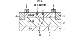
図5A及び図5Bは、第3の実施形態による化合物半導体装置の製造方法の主要工程を順に示す概略断面図である。
本実施形態では、化合物半導体装置であるAlGaN/GaN・FETの構成について、その製造方法と共に説明する。第1の実施形態とは、保護膜8の代わりに電子供給層3に空乏領域が形成される点で相違する。
図5A及び図5Bは、第3の実施形態による化合物半導体装置の製造方法の主要工程を順に示す概略断面図である。
先ず、第1の実施形態と同様に、図1A及び図1Bの各工程を経る。
続いて、図1Cと同様に、ソース電極5及びドレイン電極6を形成した後、図5Aに示すように、電子供給層3のゲート電極の形成予定部位の両側に電子線を照射する。ここで、ゲート電極の形成予定部位のドレイン電極6側のみに電子線を照射するようにしても良い。電子線照射条件としては、例えば20keV、1000μC/cm2とする。この電子線照射により、ゲート電極の形成予定部位の両側における電子供給層3の表層はダメージを受けてAlGaNの結晶構造が変質し、空乏領域31が形成される。
続いて、図1Cと同様に、ソース電極5及びドレイン電極6を形成した後、図5Aに示すように、電子供給層3のゲート電極の形成予定部位の両側に電子線を照射する。ここで、ゲート電極の形成予定部位のドレイン電極6側のみに電子線を照射するようにしても良い。電子線照射条件としては、例えば20keV、1000μC/cm2とする。この電子線照射により、ゲート電極の形成予定部位の両側における電子供給層3の表層はダメージを受けてAlGaNの結晶構造が変質し、空乏領域31が形成される。
なお、電子線を照射する代わりに、電子供給層3のゲート電極の形成予定部位の両側又はドレイン電極6側のみに、所定の元素、例えばArをイオン注入し、空乏領域を形成するようにしても良い。
しかる後、図5Bに示すように、第1の実施形態の図1Cと同様の条件により、空乏領域31と底部端で接触(又は近接)するようにゲート電極7を形成し、図1Fと同様に保護膜9を形成して(保護膜8は形成しない)、AlGaN/GaN・FETを形成する。
本実施形態によるAlGaN/GaN・FETでは、D-G間において、空乏領域31の形成されていない保護膜9の下方に相当する部分である第1の界面領域11の2次元電子ガス濃度よりも、空乏領域31の下方に相当する部分である第2の界面領域12の2次元電子ガス濃度の方が低くなる。従って、空乏領域31におけるシート抵抗は、保護膜9の直下(電子供給層3の保護膜9との接触部分)におけるシート抵抗よりも高い。
本実施形態では、ゲート電極7のドレイン電極6側の底部端における電界集中が緩和され、ゲートリーク電流が大幅に減少し、ゲート耐圧が改善される。
本実施形態では、ゲート電極7のドレイン電極6側の底部端における電界集中が緩和され、ゲートリーク電流が大幅に減少し、ゲート耐圧が改善される。
以上説明したように、本実施形態によれば、比較的簡易な構成でゲートリークを大幅に低減し、高電圧動作、高耐圧及び高出力を達成する信頼性の高いAlGaN/GaN・FETが実現する。
(第4の実施形態)
本実施形態では、電子供給層上にn型のGaN(n-Gan)層を有するn-Gan・FETの構成について、その製造方法と共に説明する。
図6A~図6Dは、第4の実施形態による化合物半導体装置の製造方法の主要工程を順に示す概略断面図である。
本実施形態では、電子供給層上にn型のGaN(n-Gan)層を有するn-Gan・FETの構成について、その製造方法と共に説明する。
図6A~図6Dは、第4の実施形態による化合物半導体装置の製造方法の主要工程を順に示す概略断面図である。
先ず、図6Aに示すように、第1の実施形態の図1Aと同様の条件でSiC基板1上に電子走行層2及び電子供給層3を形成した後、キャップ層41を形成する。
詳細には、電子供給層3上に、例えばMOVPE法により、n-Gan(例えばSiがドーピングされており、ドーピング濃度は例えば2×10¹⁸/cm3程度)を膜厚10nm以下、例えば5nm程度に堆積し、キャップ層41を形成する。キャップ層41を形成することにより、表面トラップを更に低減することができる。
詳細には、電子供給層3上に、例えばMOVPE法により、n-Gan(例えばSiがドーピングされており、ドーピング濃度は例えば2×10¹⁸/cm3程度)を膜厚10nm以下、例えば5nm程度に堆積し、キャップ層41を形成する。キャップ層41を形成することにより、表面トラップを更に低減することができる。
続いて、図6Bに示すように、ソース電極及びドレイン電極の形成予定部位に開口42を形成する。
詳細には、リソグラフィー及び塩素系ガス等を用いたドライエッチングにより、キャップ層41上のソース電極及びドレイン電極の形成予定部位に、キャップ層41下の電子供給層3の一部を掘り込む深さの開口42を形成する。
詳細には、リソグラフィー及び塩素系ガス等を用いたドライエッチングにより、キャップ層41上のソース電極及びドレイン電極の形成予定部位に、キャップ層41下の電子供給層3の一部を掘り込む深さの開口42を形成する。
続いて、図6Cに示すように、ソース電極43及びドレイン電極44を形成する。
詳細には、全面にレジストを塗布し、リソグラフィーにより、活性領域のソース電極5及びドレイン電極6の形成予定部位である開口42を露出させる開口を有するレジストパターン(不図示)を形成する。そして、例えば蒸着法により電極材料、例えばTi/Alを開口を埋め込むようにレジストパターン上に積層する。その後、加温した有機溶媒等を用いてレジストパターンをその上のTi/Alと共に除去する。その後、例えば550℃程度の温度によりSiC基板1にアニール処理を施す。以上により、開口42をTi/Alで充填して上部がキャップ層41の表面から突出する、一対のオーミック電極であるソース電極43及びドレイン電極44が形成される。
詳細には、全面にレジストを塗布し、リソグラフィーにより、活性領域のソース電極5及びドレイン電極6の形成予定部位である開口42を露出させる開口を有するレジストパターン(不図示)を形成する。そして、例えば蒸着法により電極材料、例えばTi/Alを開口を埋め込むようにレジストパターン上に積層する。その後、加温した有機溶媒等を用いてレジストパターンをその上のTi/Alと共に除去する。その後、例えば550℃程度の温度によりSiC基板1にアニール処理を施す。以上により、開口42をTi/Alで充填して上部がキャップ層41の表面から突出する、一対のオーミック電極であるソース電極43及びドレイン電極44が形成される。
しかる後、図6Dに示すように、第1の実施形態の図1Cと同様の条件によりキャップ層41上にゲート電極7を形成し、図1D~図1Fと同様に保護膜8,9を形成して、AlGaN/GaN・FETを形成する。
本実施形態によるAlGaN/GaN・FETでは、第1の実施形態と同様に、D-G間において、保護膜9の下方に相当する部分である第1の界面領域11の2次元電子ガス濃度よりも、保護膜8の下方に相当する部分である第2の界面領域12の2次元電子ガス濃度の方が低くなる。従って、保護膜8の直下(電子供給層3の保護膜8との接触部分)におけるシート抵抗は、保護膜9の直下(電子供給層3の保護膜9との接触部分)におけるシート抵抗よりも高い。
なお、本実施形態においても、第1の実施形態の変形例1と同様に、ゲート電極7をドレイン電極6側よりもソース電極5側に偏倚するように形成しても良い。
また、第1の実施形態の変形例2と同様に、保護膜8を、ゲート電極7の上面の所定部位からドレイン電極6側へ向かってゲート電極7を覆い、電子供給層3上でゲート電極7の近傍まで延在するように形成しても良い。
また、第1の実施形態の変形例3と同様に、ゲート電極7を、ドレイン電極6側よりもソース電極5側に偏倚するように形成すると共に、保護膜8を、ゲート電極7の上面の所定部位からドレイン電極6側へ向かってゲート電極7を覆い、電子供給層3上でゲート電極7の近傍まで延在するように形成しても良い。
また、第2の実施形態と同様に、保護膜8がキャップ層41上のみに存在し、ゲート電極7の底部端と接触するように、保護膜8を形成しても良い。
また、第3の実施形態と同様に、保護膜8を形成する代わりに、キャップ層41のゲート電極の形成予定部位の両側(又はドレイン電極6側のみ)に電子線を照射(又は元素をイオン注入)し、空乏領域を形成しても良い。
また、第1の実施形態の変形例2と同様に、保護膜8を、ゲート電極7の上面の所定部位からドレイン電極6側へ向かってゲート電極7を覆い、電子供給層3上でゲート電極7の近傍まで延在するように形成しても良い。
また、第1の実施形態の変形例3と同様に、ゲート電極7を、ドレイン電極6側よりもソース電極5側に偏倚するように形成すると共に、保護膜8を、ゲート電極7の上面の所定部位からドレイン電極6側へ向かってゲート電極7を覆い、電子供給層3上でゲート電極7の近傍まで延在するように形成しても良い。
また、第2の実施形態と同様に、保護膜8がキャップ層41上のみに存在し、ゲート電極7の底部端と接触するように、保護膜8を形成しても良い。
また、第3の実施形態と同様に、保護膜8を形成する代わりに、キャップ層41のゲート電極の形成予定部位の両側(又はドレイン電極6側のみ)に電子線を照射(又は元素をイオン注入)し、空乏領域を形成しても良い。
以上説明したように、本実施形態によれば、比較的簡易な構成でゲートリークを大幅に低減し、高電圧動作、高耐圧及び高出力を達成する信頼性の高いAlGaN/GaN・FETが実現する。
なお、上記した第1、第2及び第4の実施形態及び変形例では、保護膜8,9としてSiN膜を例示したが、例えば他の絶縁膜、例えばSiO2,Al2O3等を保護膜として使用しても良い。この場合、保護膜8,9を同一材料で形成するのみならず、両者を相異なる材料で形成することも考えられる。
本件によれば、比較的簡易な構成でゲートリークを大幅に低減し、高電圧動作、高耐圧及び高出力を達成する信頼性の高い化合物半導体装置が実現する。
Claims (20)
- 基板と、
前記基板上方に形成された電子走行層と、
前記電子走行層上方に形成された電子供給層と、
前記電子供給層上方に形成された、ソース電極、ドレイン電極、及び前記ソース電極と前記ドレイン電極との間に形成されたゲート電極と
を含み、
前記電子走行層と前記電子供給層との間には、前記ゲート電極と前記ドレイン電極との間において、第1の領域と、前記第1の領域よりも2次元電子ガス濃度の低い第2の領域とが形成されており、
前記第1の領域は前記ドレイン電極に偏倚する位置に、前記第2の領域は前記ゲート電極に偏倚する位置にそれぞれ形成されていることを特徴とする化合物半導体装置。 - 前記ゲート電極と前記ドレイン電極との間において、前記第1の領域の上方に相当する部分に第1の絶縁膜が、前記第2の領域の上方に相当する部分に第2の絶縁膜がそれぞれ形成されていることを特徴とする請求項1に記載の化合物半導体装置。
- 前記第2の絶縁膜は、前記第2の領域の上方に相当する部分のみに形成されていることを特徴とする請求項2に記載の化合物半導体装置。
- 前記第2の絶縁膜は、前記第2の領域の上方に相当する部分から前記ゲート電極上の少なくとも一部にかけて形成されていることを特徴とする請求項2に記載の化合物半導体装置。
- 前記第2の絶縁膜は、前記第1の絶縁膜よりも水素濃度が高いことを特徴とする請求項2に記載の化合物半導体装置。
- 前記第2の絶縁膜は、ダメージの導入により材質が変質していることを特徴とする請求項2に記載の化合物半導体装置。
- 前記電子供給層の前記ゲート電極と前記ドレイン電極との間における表層に、前記第2の領域の上方に相当する部分に結晶状態の変質による空乏領域が形成されていることを特徴とする請求項1に記載の化合物半導体装置。
- 前記電子供給層上の前記ソース電極と前記ドレイン電極との間にn型GaN層が形成されていることを特徴とする請求項1に記載の化合物半導体装置。
- 前記n型GaN層の前記ゲート電極と前記ドレイン電極との間における表層に、前記第2の領域の上方に相当する部分に結晶状態の変質による空乏領域が形成されていることを特徴とする請求項8に記載の化合物半導体装置。
- 前記ゲート電極は、前記ドレイン電極よりも前記ソース電極に偏倚した位置に形成されていることを特徴とする請求項1に記載の化合物半導体装置。
- 前記電子走行層及び前記電子供給層がそれぞれ窒化物半導体からなることを特徴とする請求項1に記載の化合物半導体装置。
- 基板と、
前記基板上方に形成された電子走行層と、
前記電子走行層上方に形成された電子供給層と、
前記電子供給層上方に形成された、ソース電極、ドレイン電極、及び前記ソース電極と前記ドレイン電極との間に形成されたゲート電極と
を含む化合物半導体装置の製造方法であって、
前記ゲート電極と前記ドレイン電極との間に、前記ゲート電極よりも前記ドレイン電極に近い位置に第1の絶縁膜を、前記ドレイン電極よりも前記ゲート電極に近い位置に第2の絶縁膜をそれぞれ形成し、
前記電子走行層と前記電子供給層との間において、前記第2の絶縁膜の下方に相当する部分の2次元電子ガス濃度を、前記第1の絶縁膜の下方に相当する部分の2次元電子ガス濃度よりも低くすることを特徴とする化合物半導体装置の製造方法。 - 前記第2の絶縁膜を、前記第1の絶縁膜よりも高い水素濃度に形成することを特徴とする請求項12に記載の化合物半導体装置の製造方法。
- 前記第2の絶縁膜を、前記第1の絶縁膜よりも高い投入電力により形成することを特徴とする請求項12に記載の化合物半導体装置の製造方法。
- 前記電子供給層上の前記ソース電極と前記ドレイン電極との間にn型GaN層が形成されていることを特徴とする請求項12に記載の化合物半導体装置の製造方法。
- 前記ゲート電極を、前記ドレイン電極よりも前記ソース電極に偏倚した位置に形成することを特徴とする請求項12に記載の化合物半導体装置の製造方法。
- 前記電子走行層及び前記電子供給層がそれぞれ窒化物半導体からなることを特徴とする請求項12に記載の化合物半導体装置の製造方法。
- 基板と、
前記基板上方に形成された電子走行層と、
前記電子走行層上方に形成された電子供給層と、
前記電子供給層上方に形成された、ソース電極、ドレイン電極、及び前記ソース電極と前記ドレイン電極との間に形成されたゲート電極と
を含む化合物半導体装置の製造方法であって、
前記電子供給層の表層に結晶状態を変質させた空乏領域を形成する工程と、
前記空乏領域が前記ドレイン電極よりも前記ゲート電極に偏倚する部位に位置するように、前記ゲート電極を形成する工程と
を含むことを特徴とする化合物半導体装置の製造方法。 - 電子線照射法又はイオン注入法により、前記空乏領域を形成することを特徴とする請求項18に記載の化合物半導体装置の製造方法。
- 前記電子走行層及び前記電子供給層がそれぞれ窒化物半導体からなることを特徴とする請求項18に記載の化合物半導体装置の製造方法。
Priority Applications (5)
| Application Number | Priority Date | Filing Date | Title |
|---|---|---|---|
| JP2011510105A JP5472293B2 (ja) | 2009-04-20 | 2009-04-20 | 化合物半導体装置及びその製造方法 |
| PCT/JP2009/057854 WO2010122628A1 (ja) | 2009-04-20 | 2009-04-20 | 化合物半導体装置及びその製造方法 |
| US13/276,830 US8581261B2 (en) | 2009-04-20 | 2011-10-19 | Compound semiconductor device and method of manufacturing the same |
| US14/050,629 US8895378B2 (en) | 2009-04-20 | 2013-10-10 | Compound semiconductor device and method of manufacturing the same |
| US14/521,978 US8999772B2 (en) | 2009-04-20 | 2014-10-23 | Compound semiconductor device and method of manufacturing the same |
Applications Claiming Priority (1)
| Application Number | Priority Date | Filing Date | Title |
|---|---|---|---|
| PCT/JP2009/057854 WO2010122628A1 (ja) | 2009-04-20 | 2009-04-20 | 化合物半導体装置及びその製造方法 |
Related Child Applications (3)
| Application Number | Title | Priority Date | Filing Date |
|---|---|---|---|
| US13276830 A-371-Of-International | 2009-04-20 | ||
| US13/276,830 Continuation US8581261B2 (en) | 2009-04-20 | 2011-10-19 | Compound semiconductor device and method of manufacturing the same |
| US14/050,629 Division US8895378B2 (en) | 2009-04-20 | 2013-10-10 | Compound semiconductor device and method of manufacturing the same |
Publications (1)
| Publication Number | Publication Date |
|---|---|
| WO2010122628A1 true WO2010122628A1 (ja) | 2010-10-28 |
Family
ID=43010766
Family Applications (1)
| Application Number | Title | Priority Date | Filing Date |
|---|---|---|---|
| PCT/JP2009/057854 Ceased WO2010122628A1 (ja) | 2009-04-20 | 2009-04-20 | 化合物半導体装置及びその製造方法 |
Country Status (3)
| Country | Link |
|---|---|
| US (3) | US8581261B2 (ja) |
| JP (1) | JP5472293B2 (ja) |
| WO (1) | WO2010122628A1 (ja) |
Cited By (8)
| Publication number | Priority date | Publication date | Assignee | Title |
|---|---|---|---|---|
| JP2012175018A (ja) * | 2011-02-24 | 2012-09-10 | Fujitsu Ltd | 化合物半導体装置 |
| WO2012132407A1 (ja) * | 2011-03-28 | 2012-10-04 | 次世代パワーデバイス技術研究組合 | 窒化物系半導体デバイス及びその製造方法 |
| JP2013219151A (ja) * | 2012-04-06 | 2013-10-24 | Sumitomo Electric Device Innovations Inc | 半導体装置 |
| WO2014185034A1 (ja) * | 2013-05-13 | 2014-11-20 | パナソニックIpマネジメント株式会社 | 半導体装置 |
| JP2015012037A (ja) * | 2013-06-26 | 2015-01-19 | 富士通株式会社 | 半導体装置及びその製造方法 |
| JP2021145050A (ja) * | 2020-03-12 | 2021-09-24 | 富士通株式会社 | 半導体装置 |
| JP2024519864A (ja) * | 2021-05-20 | 2024-05-21 | ウルフスピード インコーポレイテッド | 改善した性能を有する高電子移動度トランジスタを製造する方法 |
| JP2024519850A (ja) * | 2021-05-20 | 2024-05-21 | ウルフスピード インコーポレイテッド | 半導体表面改質を含むトランジスタ及び関連製造方法 |
Families Citing this family (12)
| Publication number | Priority date | Publication date | Assignee | Title |
|---|---|---|---|---|
| JP4897948B2 (ja) * | 2005-09-02 | 2012-03-14 | 古河電気工業株式会社 | 半導体素子 |
| JP2014138111A (ja) * | 2013-01-17 | 2014-07-28 | Fujitsu Ltd | 半導体装置及びその製造方法、電源装置、高周波増幅器 |
| JP2015056457A (ja) * | 2013-09-10 | 2015-03-23 | 株式会社東芝 | 半導体装置 |
| JP6135487B2 (ja) | 2013-12-09 | 2017-05-31 | 富士通株式会社 | 半導体装置及び半導体装置の製造方法 |
| JP6401053B2 (ja) * | 2014-12-26 | 2018-10-03 | ルネサスエレクトロニクス株式会社 | 半導体装置および半導体装置の製造方法 |
| CN105118785A (zh) * | 2015-09-02 | 2015-12-02 | 深圳大学 | 一种氮化镓异质结场效应晶体管及其形成方法 |
| JP2019517142A (ja) * | 2016-05-17 | 2019-06-20 | アメリカ合衆国 | AlGaN/GaN高電子移動度トランジスタのダメージフリープラズマCVDパッシベーション |
| US20180363314A1 (en) * | 2017-06-16 | 2018-12-20 | Cynthia Duvall | Coping Cover Assembly |
| WO2019066995A1 (en) * | 2017-09-30 | 2019-04-04 | Intel Corporation | ENHANCED RF PERFORMANCE GROUP III (III-N) NITRIDE DEVICES AND METHODS OF MAKING SAME |
| US20220139709A1 (en) * | 2020-11-05 | 2022-05-05 | International Business Machines Corporation | Confined gallium nitride epitaxial layers |
| CN116053294A (zh) * | 2021-12-31 | 2023-05-02 | 英诺赛科(苏州)科技有限公司 | 半导体器件及其制造方法 |
| US20230215939A1 (en) * | 2021-12-31 | 2023-07-06 | Innoscience (Suzhou) Technology Co., Ltd. | Semiconductor device and method for manufacturing the same |
Citations (6)
| Publication number | Priority date | Publication date | Assignee | Title |
|---|---|---|---|---|
| JP2004214471A (ja) * | 2003-01-07 | 2004-07-29 | Nec Corp | 電界効果トランジスタ |
| JP2004221325A (ja) * | 2003-01-15 | 2004-08-05 | Fujitsu Ltd | 化合物半導体装置及びその製造方法 |
| JP2005159117A (ja) * | 2003-11-27 | 2005-06-16 | Toshiba Corp | 窒化物系半導体装置 |
| WO2007040160A1 (ja) * | 2005-09-30 | 2007-04-12 | Nec Corporation | 電界効果トランジスタ |
| WO2008027027A2 (en) * | 2005-09-07 | 2008-03-06 | Cree, Inc | Transistor with fluorine treatment |
| JP2009026838A (ja) * | 2007-07-18 | 2009-02-05 | Mitsubishi Electric Corp | 半導体装置及びその製造方法 |
Family Cites Families (7)
| Publication number | Priority date | Publication date | Assignee | Title |
|---|---|---|---|---|
| JPH04282841A (ja) | 1991-03-12 | 1992-10-07 | Fujitsu Ltd | 半導体装置の製造方法 |
| JPH0818030A (ja) * | 1994-06-30 | 1996-01-19 | Fuji Electric Co Ltd | 逆導通gtoサイリスタの製造方法 |
| JP3380344B2 (ja) | 1994-11-30 | 2003-02-24 | 富士通株式会社 | 半導体装置及びその製造方法 |
| JP2004288952A (ja) | 2003-03-24 | 2004-10-14 | Fujitsu Ltd | 電界効果トランジスタ及びその製造方法 |
| US7045404B2 (en) * | 2004-01-16 | 2006-05-16 | Cree, Inc. | Nitride-based transistors with a protective layer and a low-damage recess and methods of fabrication thereof |
| JP2007227884A (ja) | 2006-01-30 | 2007-09-06 | Matsushita Electric Ind Co Ltd | 電界効果トランジスタ |
| JP2008306130A (ja) * | 2007-06-11 | 2008-12-18 | Sanken Electric Co Ltd | 電界効果型半導体装置及びその製造方法 |
-
2009
- 2009-04-20 JP JP2011510105A patent/JP5472293B2/ja active Active
- 2009-04-20 WO PCT/JP2009/057854 patent/WO2010122628A1/ja not_active Ceased
-
2011
- 2011-10-19 US US13/276,830 patent/US8581261B2/en active Active
-
2013
- 2013-10-10 US US14/050,629 patent/US8895378B2/en active Active
-
2014
- 2014-10-23 US US14/521,978 patent/US8999772B2/en active Active
Patent Citations (6)
| Publication number | Priority date | Publication date | Assignee | Title |
|---|---|---|---|---|
| JP2004214471A (ja) * | 2003-01-07 | 2004-07-29 | Nec Corp | 電界効果トランジスタ |
| JP2004221325A (ja) * | 2003-01-15 | 2004-08-05 | Fujitsu Ltd | 化合物半導体装置及びその製造方法 |
| JP2005159117A (ja) * | 2003-11-27 | 2005-06-16 | Toshiba Corp | 窒化物系半導体装置 |
| WO2008027027A2 (en) * | 2005-09-07 | 2008-03-06 | Cree, Inc | Transistor with fluorine treatment |
| WO2007040160A1 (ja) * | 2005-09-30 | 2007-04-12 | Nec Corporation | 電界効果トランジスタ |
| JP2009026838A (ja) * | 2007-07-18 | 2009-02-05 | Mitsubishi Electric Corp | 半導体装置及びその製造方法 |
Cited By (13)
| Publication number | Priority date | Publication date | Assignee | Title |
|---|---|---|---|---|
| US9093512B2 (en) | 2011-02-24 | 2015-07-28 | Fujitsu Limited | Compound semiconductor device |
| JP2012175018A (ja) * | 2011-02-24 | 2012-09-10 | Fujitsu Ltd | 化合物半導体装置 |
| WO2012132407A1 (ja) * | 2011-03-28 | 2012-10-04 | 次世代パワーデバイス技術研究組合 | 窒化物系半導体デバイス及びその製造方法 |
| JP2012204740A (ja) * | 2011-03-28 | 2012-10-22 | Advanced Power Device Research Association | 窒化物系半導体デバイス及びその製造方法 |
| JP2013219151A (ja) * | 2012-04-06 | 2013-10-24 | Sumitomo Electric Device Innovations Inc | 半導体装置 |
| WO2014185034A1 (ja) * | 2013-05-13 | 2014-11-20 | パナソニックIpマネジメント株式会社 | 半導体装置 |
| JPWO2014185034A1 (ja) * | 2013-05-13 | 2017-02-23 | パナソニックIpマネジメント株式会社 | 半導体装置 |
| JP2015012037A (ja) * | 2013-06-26 | 2015-01-19 | 富士通株式会社 | 半導体装置及びその製造方法 |
| JP2021145050A (ja) * | 2020-03-12 | 2021-09-24 | 富士通株式会社 | 半導体装置 |
| JP2024519864A (ja) * | 2021-05-20 | 2024-05-21 | ウルフスピード インコーポレイテッド | 改善した性能を有する高電子移動度トランジスタを製造する方法 |
| JP2024519850A (ja) * | 2021-05-20 | 2024-05-21 | ウルフスピード インコーポレイテッド | 半導体表面改質を含むトランジスタ及び関連製造方法 |
| JP7752704B2 (ja) | 2021-05-20 | 2025-10-10 | マコム テクノロジー ソリューションズ ホールディングス, インコーポレイテッド | 半導体表面改質を含むトランジスタ及び関連製造方法 |
| US12446252B2 (en) | 2021-05-20 | 2025-10-14 | Macom Technology Solutions Holdings, Inc. | Transistors including semiconductor surface modification and related fabrication methods |
Also Published As
| Publication number | Publication date |
|---|---|
| US8895378B2 (en) | 2014-11-25 |
| US20150044825A1 (en) | 2015-02-12 |
| US20140038372A1 (en) | 2014-02-06 |
| JPWO2010122628A1 (ja) | 2012-10-22 |
| JP5472293B2 (ja) | 2014-04-16 |
| US20120032188A1 (en) | 2012-02-09 |
| US8581261B2 (en) | 2013-11-12 |
| US8999772B2 (en) | 2015-04-07 |
Similar Documents
| Publication | Publication Date | Title |
|---|---|---|
| JP5472293B2 (ja) | 化合物半導体装置及びその製造方法 | |
| US9502524B2 (en) | Compound semiconductor device having gallium nitride gate structures | |
| JP6035007B2 (ja) | Mis型の窒化物半導体hemt及びその製造方法 | |
| US8912570B2 (en) | High electron mobility transistor and method of forming the same | |
| KR101357477B1 (ko) | 화합물 반도체 장치 및 그 제조 방법 | |
| US8766276B2 (en) | Semiconductor device and method of manufacturing semiconductor device | |
| KR101910973B1 (ko) | 고 전자 이동도 트랜지스터 및 그 제조방법 | |
| JP6051168B2 (ja) | GaNトランジスタの製造方法 | |
| US20060157735A1 (en) | Compound semiconductor device | |
| JP2004273486A (ja) | 半導体装置およびその製造方法 | |
| US10388779B2 (en) | Semiconductor device and manufacturing method thereof | |
| CN103715252A (zh) | 化合物半导体器件及其制造方法 | |
| WO2012053071A1 (ja) | 半導体装置及びその製造方法 | |
| KR101256466B1 (ko) | 질화물계 이종접합 반도체 소자 및 그 제조 방법 | |
| CN102237401A (zh) | 具有轻掺杂漏极区的高电子迁移率晶体管及其制造方法 | |
| JP5645766B2 (ja) | GaNベースの薄膜トランジスタの製造方法 | |
| JP2019114581A (ja) | 化合物半導体装置及びその製造方法 | |
| JP6236919B2 (ja) | 化合物半導体装置及びその製造方法 | |
| JP6166508B2 (ja) | 半導体装置及び半導体装置の製造方法 | |
| TW202010125A (zh) | 半導體裝置及其製造方法 | |
| US8421182B2 (en) | Field effect transistor having MOS structure made of nitride compound semiconductor | |
| JP4759923B2 (ja) | 半導体装置 | |
| TWI871161B (zh) | 功率半導體元件及用於其的製造方法 | |
| CN222547914U (zh) | 半导体器件和hemt器件 | |
| US20260122951A1 (en) | Semiconductor devices with composite dielectric layers under field plates and methods of fabrication thereof |
Legal Events
| Date | Code | Title | Description |
|---|---|---|---|
| 121 | Ep: the epo has been informed by wipo that ep was designated in this application |
Ref document number: 09843628 Country of ref document: EP Kind code of ref document: A1 |
|
| ENP | Entry into the national phase |
Ref document number: 2011510105 Country of ref document: JP Kind code of ref document: A |
|
| NENP | Non-entry into the national phase |
Ref country code: DE |
|
| 122 | Ep: pct application non-entry in european phase |
Ref document number: 09843628 Country of ref document: EP Kind code of ref document: A1 |