WO2010103695A1 - 部品内蔵モジュールの製造方法及び部品内蔵モジュール - Google Patents
部品内蔵モジュールの製造方法及び部品内蔵モジュール Download PDFInfo
- Publication number
- WO2010103695A1 WO2010103695A1 PCT/JP2009/069091 JP2009069091W WO2010103695A1 WO 2010103695 A1 WO2010103695 A1 WO 2010103695A1 JP 2009069091 W JP2009069091 W JP 2009069091W WO 2010103695 A1 WO2010103695 A1 WO 2010103695A1
- Authority
- WO
- WIPO (PCT)
- Prior art keywords
- layer
- component
- interlayer connection
- connection conductor
- manufacturing
- Prior art date
- Legal status (The legal status is an assumption and is not a legal conclusion. Google has not performed a legal analysis and makes no representation as to the accuracy of the status listed.)
- Ceased
Links
Images




Classifications
-
- H—ELECTRICITY
- H05—ELECTRIC TECHNIQUES NOT OTHERWISE PROVIDED FOR
- H05K—PRINTED CIRCUITS; CASINGS OR CONSTRUCTIONAL DETAILS OF ELECTRIC APPARATUS; MANUFACTURE OF ASSEMBLAGES OF ELECTRICAL COMPONENTS
- H05K1/00—Printed circuits
- H05K1/18—Printed circuits structurally associated with non-printed electric components
- H05K1/182—Printed circuits structurally associated with non-printed electric components associated with components mounted in printed circuit boards [PCB], e.g. insert-mounted components [IMC]
- H05K1/185—Printed circuits structurally associated with non-printed electric components associated with components mounted in printed circuit boards [PCB], e.g. insert-mounted components [IMC] associated with components encapsulated in the insulating substrate of the PCBs; associated with components incorporated in internal layers of multilayer circuit boards
-
- H—ELECTRICITY
- H05—ELECTRIC TECHNIQUES NOT OTHERWISE PROVIDED FOR
- H05K—PRINTED CIRCUITS; CASINGS OR CONSTRUCTIONAL DETAILS OF ELECTRIC APPARATUS; MANUFACTURE OF ASSEMBLAGES OF ELECTRICAL COMPONENTS
- H05K1/00—Printed circuits
- H05K1/18—Printed circuits structurally associated with non-printed electric components
- H05K1/182—Printed circuits structurally associated with non-printed electric components associated with components mounted in printed circuit boards [PCB], e.g. insert-mounted components [IMC]
- H05K1/185—Printed circuits structurally associated with non-printed electric components associated with components mounted in printed circuit boards [PCB], e.g. insert-mounted components [IMC] associated with components encapsulated in the insulating substrate of the PCBs; associated with components incorporated in internal layers of multilayer circuit boards
- H05K1/188—Printed circuits structurally associated with non-printed electric components associated with components mounted in printed circuit boards [PCB], e.g. insert-mounted components [IMC] associated with components encapsulated in the insulating substrate of the PCBs; associated with components incorporated in internal layers of multilayer circuit boards manufactured by mounting on or attaching to a structure having a conductive layer, e.g. a metal foil, such that the terminals of the component are connected to or adjacent to the conductive layer before embedding, and by using the conductive layer, which is patterned after embedding, at least partially for connecting the component
-
- H—ELECTRICITY
- H05—ELECTRIC TECHNIQUES NOT OTHERWISE PROVIDED FOR
- H05K—PRINTED CIRCUITS; CASINGS OR CONSTRUCTIONAL DETAILS OF ELECTRIC APPARATUS; MANUFACTURE OF ASSEMBLAGES OF ELECTRICAL COMPONENTS
- H05K1/00—Printed circuits
- H05K1/02—Details
- H05K1/0213—Electrical arrangements not otherwise provided for
- H05K1/0216—Reduction of cross-talk, noise or electromagnetic interference
- H05K1/023—Reduction of cross-talk, noise or electromagnetic interference using auxiliary mounted passive components or auxiliary substances
-
- H—ELECTRICITY
- H05—ELECTRIC TECHNIQUES NOT OTHERWISE PROVIDED FOR
- H05K—PRINTED CIRCUITS; CASINGS OR CONSTRUCTIONAL DETAILS OF ELECTRIC APPARATUS; MANUFACTURE OF ASSEMBLAGES OF ELECTRICAL COMPONENTS
- H05K2201/00—Indexing scheme relating to printed circuits covered by H05K1/00
- H05K2201/09—Shape and layout
- H05K2201/09209—Shape and layout details of conductors
- H05K2201/095—Conductive through-holes or vias
- H05K2201/09509—Blind vias, i.e. vias having one side closed
-
- H—ELECTRICITY
- H05—ELECTRIC TECHNIQUES NOT OTHERWISE PROVIDED FOR
- H05K—PRINTED CIRCUITS; CASINGS OR CONSTRUCTIONAL DETAILS OF ELECTRIC APPARATUS; MANUFACTURE OF ASSEMBLAGES OF ELECTRICAL COMPONENTS
- H05K2201/00—Indexing scheme relating to printed circuits covered by H05K1/00
- H05K2201/09—Shape and layout
- H05K2201/09209—Shape and layout details of conductors
- H05K2201/095—Conductive through-holes or vias
- H05K2201/09563—Metal filled via
-
- H—ELECTRICITY
- H05—ELECTRIC TECHNIQUES NOT OTHERWISE PROVIDED FOR
- H05K—PRINTED CIRCUITS; CASINGS OR CONSTRUCTIONAL DETAILS OF ELECTRIC APPARATUS; MANUFACTURE OF ASSEMBLAGES OF ELECTRICAL COMPONENTS
- H05K2201/00—Indexing scheme relating to printed circuits covered by H05K1/00
- H05K2201/10—Details of components or other objects attached to or integrated in a printed circuit board
- H05K2201/10613—Details of electrical connections of non-printed components, e.g. special leads
- H05K2201/10621—Components characterised by their electrical contacts
- H05K2201/10636—Leadless chip, e.g. chip capacitor or resistor
-
- H—ELECTRICITY
- H05—ELECTRIC TECHNIQUES NOT OTHERWISE PROVIDED FOR
- H05K—PRINTED CIRCUITS; CASINGS OR CONSTRUCTIONAL DETAILS OF ELECTRIC APPARATUS; MANUFACTURE OF ASSEMBLAGES OF ELECTRICAL COMPONENTS
- H05K2201/00—Indexing scheme relating to printed circuits covered by H05K1/00
- H05K2201/10—Details of components or other objects attached to or integrated in a printed circuit board
- H05K2201/10613—Details of electrical connections of non-printed components, e.g. special leads
- H05K2201/10621—Components characterised by their electrical contacts
- H05K2201/10674—Flip chip
-
- H—ELECTRICITY
- H05—ELECTRIC TECHNIQUES NOT OTHERWISE PROVIDED FOR
- H05K—PRINTED CIRCUITS; CASINGS OR CONSTRUCTIONAL DETAILS OF ELECTRIC APPARATUS; MANUFACTURE OF ASSEMBLAGES OF ELECTRICAL COMPONENTS
- H05K2203/00—Indexing scheme relating to apparatus or processes for manufacturing printed circuits covered by H05K3/00
- H05K2203/01—Tools for processing; Objects used during processing
- H05K2203/0191—Using tape or non-metallic foil in a process, e.g. during filling of a hole with conductive paste
-
- H—ELECTRICITY
- H05—ELECTRIC TECHNIQUES NOT OTHERWISE PROVIDED FOR
- H05K—PRINTED CIRCUITS; CASINGS OR CONSTRUCTIONAL DETAILS OF ELECTRIC APPARATUS; MANUFACTURE OF ASSEMBLAGES OF ELECTRICAL COMPONENTS
- H05K2203/00—Indexing scheme relating to apparatus or processes for manufacturing printed circuits covered by H05K3/00
- H05K2203/14—Related to the order of processing steps
- H05K2203/1461—Applying or finishing the circuit pattern after another process, e.g. after filling of vias with conductive paste, after making printed resistors
- H05K2203/1469—Circuit made after mounting or encapsulation of the components
-
- H—ELECTRICITY
- H05—ELECTRIC TECHNIQUES NOT OTHERWISE PROVIDED FOR
- H05K—PRINTED CIRCUITS; CASINGS OR CONSTRUCTIONAL DETAILS OF ELECTRIC APPARATUS; MANUFACTURE OF ASSEMBLAGES OF ELECTRICAL COMPONENTS
- H05K3/00—Apparatus or processes for manufacturing printed circuits
- H05K3/30—Assembling printed circuits with electric components, e.g. with resistors
- H05K3/32—Assembling printed circuits with electric components, e.g. with resistors electrically connecting electric components or wires to printed circuits
- H05K3/321—Assembling printed circuits with electric components, e.g. with resistors electrically connecting electric components or wires to printed circuits by conductive adhesives
-
- H—ELECTRICITY
- H05—ELECTRIC TECHNIQUES NOT OTHERWISE PROVIDED FOR
- H05K—PRINTED CIRCUITS; CASINGS OR CONSTRUCTIONAL DETAILS OF ELECTRIC APPARATUS; MANUFACTURE OF ASSEMBLAGES OF ELECTRICAL COMPONENTS
- H05K3/00—Apparatus or processes for manufacturing printed circuits
- H05K3/40—Forming printed elements for providing electric connections to or between printed circuits
- H05K3/4038—Through-connections; Vertical interconnect access [VIA] connections
- H05K3/4053—Through-connections; Vertical interconnect access [VIA] connections by thick-film techniques
- H05K3/4069—Through-connections; Vertical interconnect access [VIA] connections by thick-film techniques for via connections in organic insulating substrates
-
- Y—GENERAL TAGGING OF NEW TECHNOLOGICAL DEVELOPMENTS; GENERAL TAGGING OF CROSS-SECTIONAL TECHNOLOGIES SPANNING OVER SEVERAL SECTIONS OF THE IPC; TECHNICAL SUBJECTS COVERED BY FORMER USPC CROSS-REFERENCE ART COLLECTIONS [XRACs] AND DIGESTS
- Y02—TECHNOLOGIES OR APPLICATIONS FOR MITIGATION OR ADAPTATION AGAINST CLIMATE CHANGE
- Y02P—CLIMATE CHANGE MITIGATION TECHNOLOGIES IN THE PRODUCTION OR PROCESSING OF GOODS
- Y02P70/00—Climate change mitigation technologies in the production process for final industrial or consumer products
- Y02P70/50—Manufacturing or production processes characterised by the final manufactured product
Definitions
- the present invention relates to a method for manufacturing a component built-in module having a resin layer in which circuit components are embedded and a component built-in module.
- circuit components are embedded in a circuit board to produce a module, thereby reducing the mounting area of the circuit parts and reducing the size of the circuit board.
- a component-embedded substrate in which circuit components are embedded in a resin substrate is light in weight and does not involve high-temperature firing unlike a ceramic substrate, and thus has an advantage that there are few restrictions on the circuit components incorporated.
- a wiring pattern is formed on a release carrier, a circuit component is mounted thereon, an uncured resin layer is pressure-bonded thereon, and the circuit component is embedded in the resin layer.
- a method of manufacturing a component built-in module in which the release carrier is peeled off after being cured is disclosed.
- a wiring pattern formed on a release carrier is crimped to the component built-in module with an uncured resin layer in between, the release carrier is peeled off, and the wiring pattern is resinized. Multi-layered by transferring to a layer.
- FIG. 7 shows an example of a conventional method for manufacturing a component built-in module.
- A shows a state in which a wiring pattern (land) 51 is formed on a release carrier 50 made of a SUS plate or the like.
- B shows the state which applied the solder paste 52 on the wiring pattern 51, and mounted the circuit component 53 on it.
- C shows a state in which a metal foil 55 is pressure-bonded on the release carrier 50 with an uncured resin layer 54 therebetween, and a circuit component 53 is embedded in the resin layer 54.
- D shows a state in which the release carrier 50 is peeled after the resin layer 54 is cured.
- (E) shows a state in which a metal foil 57 is attached to the lower surface of the resin layer 54 with an uncured thin wiring layer 56 therebetween, and an interlayer connection conductor (via) 58 is formed in the thin wiring layer 56.
- (F) shows the state in which the wiring patterns 55a and 57a are formed by patterning the metal foils 55 and 57 on the front and back sides.
- the release carrier 50 such as a SUS plate is used to transfer the wiring pattern to the resin layer. Since this carrier is disposable, the material cost is high and the carrier There is a problem that electrostatic breakdown occurs when the film is peeled off or unnecessary stress is applied to the resin layer 54 and the circuit component 53. Further, since the components are mounted on the wiring pattern (land), it is necessary to form the lands larger in advance in consideration of the mounting position accuracy, and there is a limit to shortening the distance between the components. Further, when solder is used as a mounting material, there is a problem that the risk of occurrence of a short circuit due to solder flash increases. Instead of the release carrier, the core substrate is prepared in advance, the components are mounted on the wiring pattern formed on the core substrate, and then the components are embedded in the resin layer. The flash problem is not solved.
- An object of a preferred embodiment of the present invention is to provide a component built-in module manufacturing method and a component built-in module that reduce the risk of occurrence of a short circuit and the like and do not require a release carrier.
- the invention provides a method of manufacturing a component built-in module including the following steps A to C. That is, -Step A: forming a hole for an interlayer connection conductor in the first layer and filling the hole with an interlayer connection conductor made of an uncured conductive paste; -Step B: A step of mounting a circuit component on the uncured interlayer connection conductor using the tackiness of the interlayer connection conductor; Step C: a step of forming a second layer made of an uncured resin layer on the first layer and embedding the circuit component in the second layer.
- the invention according to the second embodiment provides a method of manufacturing a component built-in module including the following steps A to C. That is, -Step A: A step of fixing a circuit component on the first layer made of an uncured resin layer using the tackiness of the resin layer, -Step B: After the first layer is cured, an interlayer connection conductor hole reaching the terminal electrode of the circuit component is formed in the cured first layer, and the hole is connected to the terminal electrode of the circuit component Forming an interlayer connection conductor; Step C: a step of forming a second layer made of an uncured resin layer on the first layer before or after the step B and embedding the circuit component in the second layer.
- a wiring pattern (land) is formed on a release carrier, and circuit components are not mounted on the wiring pattern (land), but on an uncured interlayer connection conductor formed on the first layer.
- components are directly mounted using the tackiness of the interlayer connection conductor.
- the conductive paste filled in the hole for the interlayer connection conductor has a function as a component mounting material, and mounting using solder is omitted.
- a release carrier is not required, and the material cost can be greatly reduced. Also, resin filling failure due to insufficient flux cleaning does not occur because flux is not used.
- the mounting land is formed larger than the terminal electrode of the component in consideration of the mounting position accuracy of the component, and the component is mounted thereon via a bonding material such as solder.
- a bonding material such as solder.
- the first layer may be a cured substrate (ceramic substrate or resin substrate), but an uncured resin layer is used as the first layer, and circuit components are fixed using the tackiness of the resin layer. May be.
- the circuit component can be held tightly using not only the tack property of the uncured interlayer connection conductor but also the tack property of the uncured resin layer, so that the positional stability of the component is increased. There is.
- a step of simultaneously curing the first layer and the interlayer connection conductor may be provided between the step B and the step C.
- the second layer is pressure-bonded to the cured first layer and interlayer connection conductor, circuit components do not shift or come off when the second layer is pressure-bonded, and the reliability is improved.
- an interlayer connection conductor made of an uncured conductive paste may be formed so as to protrude from the surface of the first layer.
- a protective sheet such as a resin film is pasted on the surface of the first layer, and the interlayer connection is made between the first layer and the protective sheet using a laser or the like.
- the conductive paste can be filled into the interlayer connection conductor hole without damaging the first layer.
- the protective sheet is peeled off from the first layer after filling, the conductive paste protrudes from the surface of the first layer by the thickness of the protective sheet.
- the circuit component is fixed on the first layer made of the uncured resin layer using the tackiness of the resin layer, the position of the circuit component is stabilized. Further, since the first layer and the circuit component can be brought into close contact with each other, it is not necessary to consider the fluidity of the resin of the second layer under the component when forming the second layer, and the resin filling property is improved. There is an effect. There is no need to form a component mounting land on the first layer, and since the terminal electrodes of the circuit components are connected to the outside via the interlayer connection conductor formed on the first layer, the risk of solder flash generation is reduced. Can be resolved.
- a laser can be used to form the hole for the interlayer connection conductor reaching the terminal electrode of the circuit component in the first layer.
- the interlayer connection conductor hole may be plated or filled with a conductive paste.
- the step of forming a second layer of an uncured resin layer on the first layer and embedding the component in the second layer (step C) is connected to the terminal electrode of the circuit component in the cured first layer. It may be before or after the step of forming the interlayer connection conductor (step B).
- step C is performed after step B, the uncured second layer is formed on the cured first layer, so that the circuit component is already stable, and the circuit component is formed when the second layer is formed. It is difficult for deviation to occur.
- the process C is performed before the process B, the first layer and the second layer can be simultaneously cured. In that case, generation
- the first layer may be formed on the support plate, and in step B, the interlayer connection conductor may be formed so as to penetrate the support plate and the first layer.
- the support plate By providing the support plate, the stability of the first layer is improved and the component mounting accuracy is improved.
- the support plate is used as it is as a substrate or as a wiring pattern.
- a resin substrate having a thermal expansion coefficient approximate to that of the first layer and the second layer may be used. Since the thermal expansion coefficients of the support plate, the first layer, and the second layer are approximate, warpage and peeling are unlikely to occur. In that case, a wiring board having a wiring pattern on both surfaces of the resin substrate may be used as the support plate. In that case, it is not necessary to form the wiring pattern on the support plate later.
- a metal foil may be used as the support plate, and after step C, the support plate may be patterned to obtain a wiring pattern. In this case, the thickness can be further reduced as compared with the case where a resin substrate is used.
- the interlayer connection conductor and the terminal electrode of the circuit component may be bonded by solid phase diffusion.
- the conductive paste is electrically connected by physical contact between the metal fillers in the paste and between the metal filler and the counterpart conductor (terminal electrode or wiring pattern).
- an intermetallic compound is formed by solid phase diffusion between the metal filler and between the metal filler and the counterpart conductor, and a connection with lower resistance becomes possible.
- Solid phase diffusion pastes are less susceptible to changes in conductivity due to resin expansion and contraction than general contact pastes.
- solder is used on the uncured interlayer connection conductor formed in the first layer to directly mount the component using the tackiness of the interlayer connection conductor. Mounting can be omitted and the risk of solder flash can be eliminated. Also, a release carrier is not necessary, and the material cost can be greatly reduced. In addition, there is no need to form component mounting lands on the first layer, and the components are directly connected to the interlayer connection conductor, so the distance between the interlayer connection conductors can be made smaller than the distance between the lands, and further miniaturization is realized. it can.
- the circuit component is fixed on the first layer made of the uncured resin layer using the tackiness of the resin layer. Since the first layer and the circuit component are in close contact with each other, when the second layer is formed, it is not necessary to consider the fluidity of the resin of the second layer below the component, and the resin filling property is improved. Further, it is not necessary to form a component mounting land on the first layer, and the terminal electrode of the circuit component is connected to the outside via the interlayer connection conductor formed on the first layer, so that the risk of solder flash generation Can be eliminated.
- FIG. 1 shows a manufacturing process of a component built-in module including two circuit components (here, chip components).
- the number of circuit components may be one or three or more.
- the circuit component is not limited to a chip component, and may be any component such as a multi-terminal integrated circuit element or a surface wave element.
- the component built-in module in the parent board state is manufactured and then cut into the child board state.
- the resin layer 1 may be a prepreg such as a thermosetting resin sheet such as an epoxy resin or a thermosetting resin sheet containing an inorganic filler.
- the thickness of the resin layer 1 is desirably about 10 to 50 ⁇ m.
- FIG. 1B shows a second step, in which via holes (interlayer connection conductor holes) 3 are formed in the resin layer 1 including the PET films 2a and 2b.
- Arbitrary methods such as laser processing and punching, can be used for the formation method of the via hole 3.
- the via hole 3 is formed at a position corresponding to the terminal electrode of the circuit component 7 to be mounted later.
- the via hole 3 may be a tapered hole whose diameter is reduced downward.
- (C) of FIG. 1 is a 3rd process, after peeling PET film 2b by the side of the back, laminating metal foil 4, such as Cu foil, on the back surface of the resin layer 1, via the conductive paste 5 from the surface side Fill the hole 3.
- the squeegee 6 can prevent the resin layer 1 from being damaged.
- the conductive paste 5 used in this embodiment a paste containing Sn that is easy to be solid phase diffusion bonded to a Cu foil as a metal filler is desirable.
- FIG. 1 is a 4th process and shows the state which peeled PET film 2a after filling with the conductive paste (interlayer connection conductor) 5.
- FIG. A part of the conductive paste 5 protrudes from the surface of the resin layer 1 by the thickness of the PET film 2a.
- FIG. 1E shows a fifth step, in which a circuit component 7 is mounted on the conductive paste 5 protruding on the surface of the resin layer 1. Since the conductive paste 5 is in an uncured state, the circuit component 7 is held in close contact by the tackiness of the conductive paste 5. At this time, since the resin layer 1 is also in an uncured state, the circuit component 7 can be held more stably by using the tack property of the resin layer 1 by pressing the circuit component 7 until it contacts the resin layer 1. . As described above, when the via hole 3 is a tapered hole having a large diameter toward the upper side, the contact area between the terminal electrode 7a of the circuit component 7 and the conductive paste 5 is increased. 7 should be implemented.
- the tack property of the thermosetting resin contained in the conductive paste 5 and the resin layer 1 can be enhanced by performing the fifth step on a hot plate heated to a predetermined temperature (for example, 50 ° C.).
- a predetermined temperature for example, 50 ° C.
- the circuit component 7 is fixed by heating and curing the conductive paste 5 and the resin layer 1 in an oven at 180 ° C. 7 terminal electrode 7a and conductive paste 5 are electrically connected.
- a pressure for example, 2 MPa
- a conductive paste containing Sn as a metal filler conductivity can be obtained by forming an intermetallic compound by solid phase diffusion between Cu and Sn.
- This conductive paste has a feature that it is less susceptible to changes in conductivity due to expansion and contraction of the resin than a conductive paste that takes conductivity by physical contact with a metal filler as in a general contact paste.
- FIG. 1 (f) shows a sixth step, in which a metal foil 9 such as a Cu foil is pressure-bonded on the cured resin layer 1 with an uncured resin layer (second layer) 8 in between.
- the component 7 is embedded in the resin layer 8.
- the composition of the resin layer 8 is preferably the same or the same type as that of the resin layer 1.
- the resin filling is preferably performed in a state of good fluidity, for example, about 110 ° C. so that the resin wraps around the circuit component 7. Thereafter, the resin layer 8 is cured by heating to 180 ° C., whereby the resin layer 1 and the resin layer 8 are integrated, and the metal foil 9 is fixed to the surface of the resin layer 8.
- FIG. 1 (g) shows the seventh step, in which the metal foil 4 on the back surface of the resin layer 1 and the metal foil 9 on the surface of the resin layer 8 are patterned to form wiring patterns 4a and 9a.
- Complete module A shows the seventh step, in which the metal foil 4 on the back surface of the resin layer 1 and the metal foil 9 on the surface of the resin layer 8 are patterned to form wiring patterns 4a and 9a.
- the component built-in module can be manufactured without using a release carrier such as a SUS plate, the material cost can be reduced. Further, since the interlayer connection conductor (conductive paste) and the circuit component can be directly connected, mounting can be performed without using solder, the cost can be greatly reduced by reducing the number of steps, and the occurrence of solder flash can be eliminated. Furthermore, since there is no need to form lands for mounting circuit components, it is possible to cope with a narrow pitch and further reduce the size.
- the circuit component 7 is mounted in a state in which the first resin layer 1 and the conductive paste 5 are both uncured, but the conductive material is formed in the via hole 3 of the cured or semi-cured resin layer 1.
- the paste 5 may be filled and the circuit component 7 may be mounted on the conductive paste 5.
- the circuit component 7 is held only by the tackiness of the conductive paste 5.
- the uncured resin layer 8 is pressure-bonded on the cured resin layer 1 in the step (f)
- the strength of the circuit component 7 does not cause displacement or dropping when the resin layer 8 is pressure-bonded. If it has, the resin layer 1 and the conductive paste 5 do not need to be completely cured, and may be in a semi-cured state. In that case, since the resin layer 1 and the resin layer 8 can be hardened simultaneously, generation
- FIG. 2 shows a second embodiment of a component built-in module manufactured by a method similar to the manufacturing method according to the first embodiment, and uses a circuit element 10 having a plurality of terminals on the lower surface as a circuit component.
- This component built-in module B has a plurality of terminal electrodes 11 on the lower surface of the circuit element 10, and these terminal electrodes 11 are directly connected to the conductive paste 5 which is an interlayer connection conductor. Therefore, it can be mounted without solder balls, and the thickness of the component built-in module B can be reduced accordingly.
- FIG. 2 there is a gap between the lower surface of the circuit element 10 and the resin layer 1, and the gap is filled with the resin layer 8, but the lower surface of the circuit element 10 and the resin layer 1 are in contact with each other. There may be.
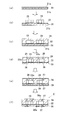
- FIG. 3 shows a third embodiment of a method for manufacturing a component built-in module according to the present invention, and this embodiment corresponds to claim 6.
- a cured resin substrate (support plate) 20 having PET films 21a and 21b attached to the front and back surfaces is prepared.
- the resin substrate 20 a thermosetting resin substrate such as an epoxy resin, a thermosetting resin substrate containing an inorganic filler, or the like can be used.
- the PET film 21a on the surface side is peeled off, and instead an adhesive layer (first layer) 22 is formed by a printing method or the like.
- the state where the circuit component 23 is bonded and fixed is shown. At this time, the entire lower surface of the circuit component 23 is brought into close contact with the adhesive layer 22.
- the material of the adhesive layer 22 is preferably the same as that of the resin substrate 20. After the circuit component 23 is mounted, the adhesive layer 22 is cured by heating.
- FIG. 3C shows a state in which an uncured resin layer (second layer) 24 is pressure-bonded on the resin substrate 20 and the circuit component 23 is embedded in the resin layer 24.
- the composition of the resin layer 24 is preferably the same or the same type as that of the resin substrate 20.
- the resin filling is preferably performed in a state of good fluidity, for example, about 110 ° C. so that the resin wraps around the circuit component 23.
- the resin layer 24 is cured by heating to 180 ° C., whereby the resin substrate 20 and the resin layer 24 are integrated to form a multilayer substrate.
- via holes (interlayer connection conductor holes) 25 and 26 extending from the upper side of the resin layer 24 and the lower side of the resin substrate 20 to the terminal electrodes 23a of the circuit component 23 are formed by laser processing. After laser processing, desmear processing is performed.
- filled plating is performed on the via holes 25 and 26.
- the metal material (interlayer connection conductor) 27 can be filled in the via holes 25 and 26 on both sides of the front and back, and at the same time, the metal coating 28 is formed on the front and back surfaces (the upper surface of the resin layer 24 and the lower surface of the resin substrate 20). Can be formed. Thereby, the metal coating 28 and the circuit component 23 are electrically connected.
- the conductive holes may be filled in the via holes 25 and 26 on both sides of the front and back sides.
- the component built-in module C is completed by patterning the metal film 28 on the front and back surfaces to form a wiring pattern 28a.
- the via holes 25 and 26 are formed in both the resin substrate 20 and the resin layer 24.
- the via holes 25 in the resin layer 24 are not essential.
- the via hole 26 of the resin substrate 20 is processed after the resin layer 24 is formed, it can be processed before the resin layer 24 is formed.
- the cured resin substrate 20 is used as a core substrate, the adhesive layer 22 is formed thereon, the circuit component 23 is disposed thereon, and the adhesive layer 22 is cured by applying heat.
- Vias are formed on both sides of the resin-molded multilayer substrate from the both sides to the terminal electrodes of the circuit components, and the plating is filled simultaneously on both sides to establish connection.
- the resin substrate 20 which is a core substrate as a support material, the component built-in module C can be manufactured without requiring a release carrier.
- the lands need to be formed larger in consideration of mounting position accuracy.
- via holes 25 and 26 that reach the terminal electrodes 23a later are opened and connected. Therefore, the pitch can be further reduced. Since the filled plating method is used as a method for forming a conductor in the via hole, the filling of the via hole on both the front and back surfaces and the metal film can be simultaneously formed, and the number of processing steps can be reduced.
- FIG. 4 shows a fourth embodiment of the method for manufacturing a component built-in module according to the present invention, and this embodiment corresponds to claim 8.
- a cured resin substrate (support plate) 30 having metal foils 31 and 32 such as Cu foil attached to the front and back surfaces is prepared.
- the metal foils 31 and 32 on both the front and back surfaces are patterned by etching or the like to form wiring patterns 31a and 32a.
- the formation method of the wiring patterns 31a and 32a is not limited to etching, and may be formed on the resin substrate 30 by plating or the like.
- an uncured adhesive layer (first layer) 33 is formed on the resin substrate 30 so as to cover the wiring pattern 31a by printing or the like, and the circuit component 34 is bonded and fixed thereon. .
- the circuit component 34 is fixed so as to correspond to a predetermined position on the wiring pattern 31a, but the terminal electrode 34a of the circuit component 34 and the wiring pattern 31a are not in contact with each other.
- the adhesive layer 33 does not have to be the entire surface of the resin substrate 30 and may be only the mounting portion of the circuit component 34. Since the entire lower surface of the circuit component 34 is held by the tackiness of the adhesive layer 33, the circuit component 34 is stabilized. In this state, the adhesive layer 33 is thermally cured.
- an uncured resin layer (second layer) 35 is pressure-bonded on the resin substrate 30, and the circuit component 34 is embedded in the resin layer 35.
- the composition of the resin layer 35 is preferably the same or the same type as that of the resin substrate 30.
- the resin filling is preferably performed in a state of good fluidity, for example, about 110 ° C. so that the resin wraps around the circuit component 34.
- the resin layer 35 is cured by heating to 180 ° C., whereby the resin substrate 30 and the resin layer 35 are integrated to form a multilayer substrate.
- via holes (interlayer connection conductor holes) 36 and 37 extending from the upper side of the resin layer 35 and the lower side of the resin substrate 30 to the terminal electrodes 34a of the circuit component 34 are formed by laser processing. At this time, by irradiating the laser using the opening of the wiring pattern 32a on the back surface, the wiring pattern 32a is not damaged. After laser processing, desmear processing is performed.
- the via holes 36 and 37 include a via hole 36 a extending from the upper surface of the resin layer 35 to the wiring pattern 31 a and a via hole 37 a extending from the lower surface of the resin substrate 30 to the wiring pattern 31 a.
- filled plating is performed on the via holes 36 and 37.
- the metal material (interlayer connection conductor) 38 can be filled in the via holes 36 and 37 on both sides of the front and back, and at the same time, the metal film 39 is formed on the front and back surfaces (the upper surface of the resin layer 35 and the lower surface of the resin substrate 30). Can be formed.
- the metal coating 39 and the circuit component 34 are electrically connected via the interlayer connection conductor 38.
- the via holes 36 and 37 on both sides may be filled with a conductive paste.
- the metal film 39 on the front and back surfaces is patterned to form a wiring pattern 39a, thereby completing the component built-in module D.
- the via holes 36 and 37 are formed in both the resin substrate 30 and the resin layer 35.
- the via hole 36 in the resin layer 35 is not essential.
- the via hole 37 of the resin substrate 30 is processed after the formation of the resin layer 35, it can be processed before the formation of the resin layer 35.
- FIG. 5 shows a fifth embodiment of the method for manufacturing a component built-in module according to the present invention, and this embodiment corresponds to claim 9.
- an adhesive (first layer) 41 is applied on a metal foil (support plate) 40 such as a Cu foil by using a printing method, a dispenser, or the like.
- a metal foil (support plate) 40 such as a Cu foil by using a printing method, a dispenser, or the like.
- the adhesive 41 is applied only to the component mounting portion here, it may be applied to the entire surface.
- the surface of the metal foil 40 may be subjected to a roughening process for increasing the adhesion strength.
- the circuit component 42 is bonded and fixed on the adhesive 41 using its tackiness. Thereafter, the adhesive 41 is heated to 130 to 150 ° C. and thermally cured. At this stage, the terminal electrode 42a of the circuit component 42 and the metal foil 40 are not connected.
- the uncured resin layer (second layer) 43 and the metal foil 44 are stacked and pressure-bonded on the metal foil 40, and the circuit component 42 is embedded in the resin layer 43.
- the resin filling is preferably performed in a state of good fluidity, for example, about 110 ° C. so that the resin wraps around the circuit component 42.
- the resin layer 43 is cured by heating to 180 ° C., whereby the adhesive 41 and the resin layer 43 are integrated, and a substrate having the metal foils 40 and 44 on the front and back is formed.
- via holes (interlayer connection conductor holes) 45 and 46 extending from the upper and lower sides of the resin layer 43 to the terminal electrodes 42a of the circuit component 42 are formed by laser processing.
- the metal foils 40 and 44 formed on the front and back surfaces are used as a conformal mask, or laser vias are formed for each metal foil using the DLD method. After laser processing, desmear processing is performed.
- filled plating is performed on the via holes 45, 46, and the via holes 45, 46 on both sides of the front and back sides are filled with a metal material (interlayer connection conductor) 47. 44.
- the metal foils 40 and 44 and the circuit component 42 are electrically connected via the interlayer connection conductor 47.
- the via holes 45 and 46 on both sides may be filled with a conductive paste.
- the component built-in module E is completed by patterning the metal foils 40 and 44 on the front and back surfaces to form the wiring patterns 40a and 44a.
- the via holes 45 and 46 extending from both the upper and lower sides of the resin layer 43 to the circuit component 42 are formed.
- at least one of the via holes 45 and 46 is formed so as to penetrate the resin layer 43 in the vertical direction.
- the metal foils 40 and 44 on the front and back surfaces may be made conductive.
- a mounting pattern (land) by additive plating or etching on the metal foil that becomes a support at the time of mounting.
- a mounting substrate As a mounting substrate, only an adhesive is applied, and a mounting pattern forming step is not required. Further, it becomes unnecessary for a bonding agent such as solder and flux, and a reflow and flux cleaning process. Since the lower surface of the circuit component 42 is filled with the adhesive 41, no filling failure occurs when the circuit component 42 is built in the resin layer 43. Since the metal foil is used as a mounting substrate and used as a wiring material, material loss is reduced. Since the via exists only on the terminal electrode, high-density mounting is possible without considering the via arrangement.
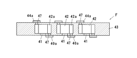
- FIG. 6 shows a sixth embodiment of a component built-in module manufactured by the same method as that of the fifth embodiment.
- this component built-in module F an adhesive 41 for fixing the circuit component 42 is applied only to the gap portion (portion where there is no terminal electrode) of the circuit component 42.
- the terminal electrode 42 a does not touch the adhesive 41, and the periphery of the terminal electrode 42 a is covered with a built-in resin layer 43.
- the upper and lower surfaces of the resin are the same, so that processing can be performed under the same conditions.
- the adhesion strength with the adhesive 41 can be applied only to the exposed upper surface side in the fifth embodiment. In this embodiment, the entire surface of the terminal electrode can be processed.
- a to F Component built-in module 1 Resin layer (first layer) 2a, 2b Carrier film 3 Via hole (interlayer connection conductor hole) 4 Metal foil (copper foil) 4a Wiring pattern 5 Conductive paste (interlayer connection conductor) 7 Circuit component 7a Terminal electrode 8 Resin layer (second layer) 9 Metal foil (copper foil) 9a Wiring pattern 10, 23, 34 Circuit component (multi-terminal circuit element) 20, 30 Cured resin substrate (support plate) 22, 33 Adhesive layer (first layer) 23, 34 Circuit parts 24, 35 Resin layer (second layer) 25, 26, 36, 37 Via hole (interlayer connection conductor hole) 27,38 Metal material (interlayer connection conductor) 28, 39 Metal coating 28a, 39a Wiring pattern
Landscapes
- Engineering & Computer Science (AREA)
- Microelectronics & Electronic Packaging (AREA)
- Manufacturing & Machinery (AREA)
- Production Of Multi-Layered Print Wiring Board (AREA)
Abstract
【課題】ショート等の発生リスクを低減し、離型キャリアを必要としない部品内蔵モジュールの製造方法を提供する。 【解決手段】未硬化の樹脂層よりなる第1層1に層間接続導体用孔3を形成し、この孔に未硬化の導電性ペーストよりなる層間接続導体5を充填する。次に、未硬化の層間接続導体5上に、当該層間接続導体のタック性を利用して回路部品7を実装し、第1層1と層間接続導体5とを硬化させる。硬化後、第1層上に未硬化の樹脂層よりなる第2層8を形成し、回路部品7を第2層8中に埋設する。このように未硬化の層間接続導体上に部品を直接実装するため、はんだを用いた実装を省略でき、はんだフラッシュの発生リスクを解消できる。さらに、離型キャリアも不要になり、材料費の大幅なコストダウンが図れる。
Description
本発明は、内部に回路部品が埋設された樹脂層を有する部品内蔵モジュールの製造方法及び部品内蔵モジュールに関するものである。
近年、電子機器の小型化に伴い、回路基板内部に回路部品を埋設してモジュールを作製することにより、回路部品の実装面積を削減し、回路基板の小型化を図ることが行われている。中でも、樹脂基板の内部に回路部品が埋設された部品内蔵基板は、軽量であり、かつセラミック基板のように高温焼成を伴わないため、内蔵する回路部品に制約が少ないという利点がある。
特許文献1には、離型キャリア上に配線パターンを形成し、その上に回路部品を実装し、その上に未硬化の樹脂層を圧着して回路部品を樹脂層に埋設し、樹脂層を硬化させた後で離型キャリアを剥離する部品内蔵モジュールの製造方法が開示されている。部品内蔵モジュールを多層化するには、離型キャリア上に配線パターンを形成したものを、未硬化の樹脂層を間にして部品内蔵モジュールに圧着し、離型キャリアを剥離して配線パターンを樹脂層に転写することにより、多層化している。
図7は、従来の部品内蔵モジュールの製造方法の一例を示す。(a)はSUS板等よりなる離型キャリア50に配線パターン(ランド)51を形成した状態を示す。(b)は配線パターン51上にはんだペースト52を塗布し、その上に回路部品53を実装した状態を示す。(c)は離型キャリア50上に未硬化の樹脂層54を間にして金属箔55を圧着し、樹脂層54の内部に回路部品53を埋設した状態を示す。(d)は樹脂層54の硬化後に離型キャリア50を剥離する状態を示す。(e)は樹脂層54の下面に未硬化の薄層配線層56を間にして金属箔57を貼り付けると共に、薄層配線層56に層間接続導体(ビア)58を形成した状態を示す。(f)は表裏の金属箔55,57をパターニングして配線パターン55a,57aを形成した状態を示す。
上述のように、従来の方法では配線パターンを樹脂層に対して転写するためにSUS板などの離型キャリア50を用いており、このキャリアは使い捨てであるため、高い材料費がかかると共に、キャリアを剥離する際に静電気破壊が発生したり、不必要な応力が樹脂層54や回路部品53にかかるという問題がある。また、部品を配線パターン(ランド)に実装するため、実装位置精度を考慮してランドを予め大きめに形成する必要があり、部品間距離を短縮するには限界があった。さらに、実装材料としてはんだを使用した場合には、はんだフラッシュによるショートの発生リスクが高くなるという問題があった。離型キャリアに代えて、コア基板を予め作成し、コア基板上に形成された配線パターンに部品を実装し、その後、部品を樹脂層に埋設する方法を採った場合でも、部品間距離やはんだフラッシュの問題は解決されない。
本発明の好ましい実施形態の目的は、ショート等の発生リスクを低減し、離型キャリアを必要としない部品内蔵モジュールの製造方法及び部品内蔵モジュールを提供することにある。
前記目的を達成するため、第1の実施形態に係る発明は以下のA~Cの工程を含む部品内蔵モジュールの製造方法を提供する。すなわち、
-工程A:第1層に層間接続導体用孔を形成し、この孔に未硬化の導電性ペーストよりなる層間接続導体を充填する工程、
-工程B:前記未硬化の層間接続導体上に、当該層間接続導体のタック性を利用して回路部品を実装する工程、
-工程C:前記第1層上に未硬化の樹脂層よりなる第2層を形成し、前記回路部品を第2層中に埋設する工程。
-工程A:第1層に層間接続導体用孔を形成し、この孔に未硬化の導電性ペーストよりなる層間接続導体を充填する工程、
-工程B:前記未硬化の層間接続導体上に、当該層間接続導体のタック性を利用して回路部品を実装する工程、
-工程C:前記第1層上に未硬化の樹脂層よりなる第2層を形成し、前記回路部品を第2層中に埋設する工程。
第2の実施形態に係る発明は以下のA~Cの工程を含む部品内蔵モジュールの製造方法を提供する。すなわち、
-工程A:未硬化の樹脂層よりなる第1層上に、当該樹脂層のタック性を利用して回路部品を固定する工程、
-工程B:前記第1層を硬化させた後、硬化した第1層に前記回路部品の端子電極に至る層間接続導体用孔を形成し、この孔に前記回路部品の端子電極に接続される層間接続導体を形成する工程、
-工程C:工程Bの前又は後に、前記第1層の上に未硬化の樹脂層よりなる第2層を形成し、前記回路部品を第2層中に埋設する工程。
-工程A:未硬化の樹脂層よりなる第1層上に、当該樹脂層のタック性を利用して回路部品を固定する工程、
-工程B:前記第1層を硬化させた後、硬化した第1層に前記回路部品の端子電極に至る層間接続導体用孔を形成し、この孔に前記回路部品の端子電極に接続される層間接続導体を形成する工程、
-工程C:工程Bの前又は後に、前記第1層の上に未硬化の樹脂層よりなる第2層を形成し、前記回路部品を第2層中に埋設する工程。
第1の実施形態に係る発明では、離型キャリア上に配線パターン(ランド)を形成し、その上に回路部品を実装するのではなく、第1層に形成された未硬化の層間接続導体上に、当該層間接続導体のタック性を利用して部品を直接実装している。つまり、層間接続導体用孔に充填された導電性ペーストに部品実装材料としての機能を持たせ、はんだを用いた実装を省略している。そのため、はんだフラッシュによるショートの発生リスクを解消できる。さらに、離型キャリアも不要になり、材料費の大幅なコストダウンを図ることができる。また、フラックス洗浄不足による樹脂充填不良も、フラックスを用いないため発生しない。
一般に、実装用ランドは部品の実装位置精度を考慮して、部品の端子電極より大きめに形成されており、その上にはんだ等の接合材を介して部品が実装される。部品の小型化が進むと、ランド間距離も狭める必要があるが、ランドの形状が部品の端子電極より大きいため、部品間距離を狭くするには限界があった。本発明では、部品実装用ランドを形成する必要がなく、層間接続導体に部品が直接接続される。層間接続導体(ビア)の面積はランドに比べて小形に形成できるので、層間接続導体間距離を狭めることができ、さらなる小型化を実現できる。
第1層は硬化済みの基板(セラミック基板又は樹脂基板)であってもよいが、第1層として未硬化の樹脂層を使用し、当該樹脂層のタック性を利用して回路部品を固定してもよい。この場合には、未硬化の層間接続導体のタック性だけでなく、未硬化の樹脂層のタック性も利用して回路部品を密着保持することができるので、部品の位置安定性が増すという利点がある。なお、樹脂層及び導電性ペーストのタック性を高めるため、所定温度(例えば50℃~70℃程度)に加熱した状態で回路部品を固定するのがよい。
前述のように第1層も未硬化の樹脂層である場合、工程Bと工程Cとの間に、第1層及び層間接続導体を同時に硬化させる工程を有してもよい。この場合には、硬化した第1層及び層間接続導体に対して第2層を圧着するので、第2層の圧着時に回路部品のずれや外れが発生せず、信頼性が向上する。
工程Aにおいて、未硬化の導電性ペーストよりなる層間接続導体を第1層の表面から突出するように形成してもよい。層間接続導体用孔に導電性ペーストを充填する方法として、例えば第1層の表面に樹脂フィルムのような保護シートを貼り付けておき、レーザ等を用いて第1層と保護シートとに層間接続導体用孔を形成し、その上から導電性ペーストをスキージングすることで、第1層を傷つけずに層間接続導体用孔に導電性ペーストを充填することができる。この場合、充填後に保護シートを第1層から剥離すると、保護シートの厚み分だけ導電性ペーストが第1層の表面から突出する。このように突出させた導電性ペーストに対して回路部品を押しつけると、導電性ペーストと回路部品の端子電極との接触面積が増大するので、接続信頼性が向上する利点がある。
第2の実施形態に係る発明では、未硬化の樹脂層よりなる第1層上に、回路部品が樹脂層のタック性を利用して固定されるため、回路部品の位置が安定する。また、第1層と回路部品とを密着させることができるので、第2層を形成する際、部品下への第2層の樹脂の流動性を考慮する必要がなく、樹脂充填性が向上するという効果がある。第1層には部品実装用ランドを形成しておく必要がなく、第1層に形成された層間接続導体を介して回路部品の端子電極が外部と接続されるので、はんだフラッシュの発生リスクを解消できる。
第1層に回路部品の端子電極に至る層間接続導体用孔を形成するには、レーザを使用することができる。部品の端子電極に接続される層間接続導体を形成するために、層間接続導体用孔にめっきを行ってもよいし、導電ペーストを充填してもよい。第1層の上に未硬化の樹脂層よりなる第2層を形成し、部品を第2層中に埋設する工程(工程C)は、硬化した第1層に回路部品の端子電極に接続される層間接続導体を形成する工程(工程B)の前でもよいし、後でもよい。工程Cを工程Bの後で実施する場合には、硬化した第1層の上に未硬化の第2層を形成するため、回路部品が既に安定しており、第2層の形成時に回路部品のずれが発生しにくい。一方、工程Cを工程Bの前に実施する場合には、第1層と第2層とを同時に硬化させることも可能である。その場合には、反りの発生を抑制できる。
工程Aの前に、支持板上に第1層を形成し、工程Bにおいて、層間接続導体を支持板及び第1層を貫通するように形成してもよい。支持板を設けることで、第1層の安定性が向上し、部品の搭載精度が向上する。支持板とは、離型キャリアとは異なり、そのまま基板として使用されるか、あるいは配線パターンとして使用される。
支持板は、第1層及び第2層と近似した熱膨張係数を有する樹脂基板を使用してもよい。支持板と第1層、第2層の熱膨張係数が近似するため、反りや剥離が発生しにくい。その場合、支持板として、樹脂基板の両面に配線パターンを有する配線基板を使用してもよく、その場合には後で支持板に配線パターンを形成する必要がない。
支持板として金属箔を使用し、工程Cの後に、支持板をパターン化して配線パターンを得てもよい。この場合には、樹脂基板を用いる場合に比べてさらに薄型化できる。
工程Bにおいて、層間接続導体と回路部品の端子電極とを固相拡散接合させてもよい。通常、導電性ペーストとは、ペースト中の金属フィラー同士及び金属フィラーと相手の導体(端子電極又は配線パターン)とが物理的に接触することによって導通を取っている。金属フィラーの組成を工夫することによって、金属フィラー間及び金属フィラーと相手の導体との間に固相拡散による金属間化合物が形成され、より抵抗の低い接続が可能になる。固相拡散ペーストの場合、一般的なコンタクト型ペーストに比べて、樹脂の膨張、収縮による導電性の変化を受けにくい特徴がある。
第2層に、回路部品の端子電極に接続される層間接続導体を形成する工程をさらに備えてもよい。部品の端子電極を利用して第2層上面の配線パターンと層間接続することができるので、部品内蔵モジュールのさらなる多機能化、小型化を実現できる。
第1の実施形態に係る発明によれば、第1層に形成された未硬化の層間接続導体上に、その層間接続導体のタック性を利用して部品を直接実装するため、はんだを用いた実装を省略でき、はんだフラッシュの発生リスクを解消できる。また、離型キャリアも不要になり、材料費の大幅なコストダウンを図ることができる。さらに、第1層に部品実装用ランドを形成する必要がなく、層間接続導体に部品が直接接続されるので、層間接続導体間の距離をランド間距離より狭めることができ、さらなる小型化を実現できる。
第2の実施形態に係る発明によれば、未硬化の樹脂層よりなる第1層上に回路部品を樹脂層のタック性を利用して固定するので、回路部品の位置が安定すると共に、第1層と回路部品とが密着するので、第2層を形成する際、部品下への第2層の樹脂の流動性を考慮する必要がなく、樹脂充填性が向上する。また、第1層に部品実装用ランドを形成しておく必要がなく、第1層に形成された層間接続導体を介して回路部品の端子電極が外部と接続されるので、はんだフラッシュの発生リスクを解消できる。
〔実施例1〕
本発明に係る部品内蔵モジュールの製造方法の第1実施例について、図1を参照しながら説明する。この実施例は、請求項1、2に対応するものである。説明を簡単にするため、図1では2個の回路部品(ここではチップ部品)を含む部品内蔵モジュールの製造工程を示しているが、回路部品は1個又は3個以上であってもよい。回路部品はチップ部品に限らず、多端子の集積回路素子や表面波素子等、如何なる部品でもよい。なお、実際の製造工程では、親基板状態の部品内蔵モジュールが作製され、その後で子基板状態にカットされる。
本発明に係る部品内蔵モジュールの製造方法の第1実施例について、図1を参照しながら説明する。この実施例は、請求項1、2に対応するものである。説明を簡単にするため、図1では2個の回路部品(ここではチップ部品)を含む部品内蔵モジュールの製造工程を示しているが、回路部品は1個又は3個以上であってもよい。回路部品はチップ部品に限らず、多端子の集積回路素子や表面波素子等、如何なる部品でもよい。なお、実際の製造工程では、親基板状態の部品内蔵モジュールが作製され、その後で子基板状態にカットされる。
図1の(a)は第1工程であり、表裏面にPETフィルム2a,2bを貼り付けた薄肉な未硬化の樹脂層(第1層)1を準備する。樹脂層1は、エポキシ樹脂などの熱硬化性樹脂シート、無機フィラーを含む熱硬化性樹脂シートといったプリプレグが使用できる。樹脂層1の厚みは、10~50μm程度が望ましい。
図1の(b)は第2工程であり、PETフィルム2a,2bを含む樹脂層1に対してビア孔(層間接続導体用孔)3を形成する。ビア孔3の形成方法は、レーザー加工、パンチング等の任意の方法を用いることができる。ビア孔3は、後で実装される回路部品7の端子電極と対応する位置に形成される。レーザー加工を用いた場合は、ビア孔3が下方に向かって縮径するテーパ状の穴になることがある。
図1の(c)は第3工程であり、裏面側のPETフィルム2bを剥離し、樹脂層1の裏面にCu箔などの金属箔4をラミネートした後、表面側から導電性ペースト5をビア孔3に対して充填する。このとき、表面側のPETフィルム2aを貼り付けたまま充填するので、スキージ6によって樹脂層1が傷つくのを防止できる。この実施例で使用する導電性ペースト5としては、金属フィラーとしてCu箔に対して固相拡散接合しやすいSnを含むペーストが望ましい。
図1の(d)は第4工程であり、導電性ペースト(層間接続導体)5を充填した後、PETフィルム2aを剥離した状態を示す。樹脂層1の表面から導電性ペースト5の一部が、PETフィルム2aの厚み分だけ突出している。
図1の(e)は第5工程であり、樹脂層1の表面に突出している導電性ペースト5に対して回路部品7を搭載した状態を示す。導電性ペースト5は未硬化状態であるため、導電性ペースト5のタック性によって回路部品7は密着保持される。このとき、樹脂層1も未硬化状態であるから、回路部品7を樹脂層1と接触するまで圧着することで、樹脂層1のタック性を利用して回路部品7をさらに安定して保持できる。上述のようにビア孔3が上方に向かって大径となるテーパ孔の場合、回路部品7の端子電極7aと導電性ペースト5との接触面積を大きくするため、ビア孔3の上側に回路部品7を実装するのがよい。
なお、第5工程を所定温度(例えば50℃)に加熱したホットプレート上で実施することで、導電性ペースト5及び樹脂層1に含まれる熱硬化性樹脂のタック性を高めることができる。回路部品7を導電性ペースト5及び樹脂層1に対して圧着した状態で、180℃のオーブンで導電性ペースト5及び樹脂層1を加熱硬化させることで、回路部品7は固定され、かつ回路部品7の端子電極7aと導電ペースト5とが電気的に接続される。この時、部品が壊れたり、樹脂が部品周辺から流動しない程度の圧力(例えば2MPa)をかけながら実施するのがよい。上述のように、金属フィラーとしてSnを含む導電性ペーストを使用した場合、Cu-Sn間で固相拡散による金属間化合物の形成により導電性をとることができる。この導電性ペーストは、一般的なコンタクト型ペーストのように金属フィラーの物理的な接触により導電性をとるものに比べて、樹脂の膨張、収縮による導電性の変化を受けにくい特徴がある。
図1の(f)は第6工程であり、硬化済みの樹脂層1の上に、未硬化の樹脂層(第2層)8を間にしてCu箔などの金属箔9を圧着し、回路部品7をこの樹脂層8の中に埋設する。樹脂層8の組成は樹脂層1と同質または同種のものがよい。樹脂充填は、回路部品7の周囲に樹脂が回り込むように、例えば110℃程度の流動性のよい状態で行うのがよい。その後、180℃に加熱して樹脂層8を硬化させることで、樹脂層1と樹脂層8とが一体化されると共に、樹脂層8の表面に金属箔9が固着される。
図1の(g)は第7工程であり、樹脂層1の裏面の金属箔4と樹脂層8の表面の金属箔9とをパターニングし、配線パターン4a、9aを形成することで、部品内蔵モジュールAを完成する。
上述のように、SUS板等の離型キャリアを使用せずに部品内蔵モジュールを作製できるので、材料コストを低減できる。また、層間接続導体(導電性ペースト)と回路部品とを直接接続できるので、はんだを使用せずに実装でき、工数の減少によってコストを大幅に低減できると共に、はんだフラッシュの発生を解消できる。さらに、回路部品を実装するためのランドを形成する必要がないので、狭ピッチ化に対応でき、さらなる小型化が可能になる。
第1実施例では、第1層の樹脂層1と導電ペースト5とが共に未硬化の状態で回路部品7を搭載したが、硬化済み又は半硬化状態の樹脂層1のビア孔3に導電性ペースト5を充填し、その導電性ペースト5上に回路部品7を搭載してもよい。この場合には、導電性ペースト5のタック性だけで回路部品7は保持される。さらに、工程(f)において硬化済みの樹脂層1の上に未硬化の樹脂層8を圧着したが、樹脂層8を圧着した際に回路部品7の位置ずれや脱落を生じない程度の強度を有しておれば、樹脂層1及び導電性ペースト5は完全硬化している必要はなく、半硬化状態でもよい。その場合には、樹脂層1と樹脂層8とを同時に硬化させることができるので、反りの発生を抑制できる。
〔実施例2〕
図2は、第1実施例による製造方法と同様の方法で製造した部品内蔵モジュールの第2実施例を示し、回路部品として下面に複数の端子を有する回路素子10を使用したものである。この部品内蔵モジュールBでは、回路素子10の下面に複数の端子電極11を有し、これら端子電極11が層間接続導体である導電性ペースト5と直接接続されている。そのため、半田ボールなしで実装でき、その分、部品内蔵モジュールBの厚みを薄くできる。図2では、回路素子10の下面と樹脂層1との間に隙間が存在し、その隙間に樹脂層8が充填されているが、回路素子10の下面と樹脂層1とが接触した状態であってもよい。
図2は、第1実施例による製造方法と同様の方法で製造した部品内蔵モジュールの第2実施例を示し、回路部品として下面に複数の端子を有する回路素子10を使用したものである。この部品内蔵モジュールBでは、回路素子10の下面に複数の端子電極11を有し、これら端子電極11が層間接続導体である導電性ペースト5と直接接続されている。そのため、半田ボールなしで実装でき、その分、部品内蔵モジュールBの厚みを薄くできる。図2では、回路素子10の下面と樹脂層1との間に隙間が存在し、その隙間に樹脂層8が充填されているが、回路素子10の下面と樹脂層1とが接触した状態であってもよい。
〔実施例3〕
図3は、本発明に係る部品内蔵モジュールの製造方法の第3実施例を示し、この実施例は請求項6に対応するものである。図3の(a)では、表裏面にPETフィルム21a,21bを貼り付けた硬化済みの樹脂基板(支持板)20を準備する。樹脂基板20としては、エポキシ樹脂などの熱硬化性樹脂基板、無機フィラーを含む熱硬化性樹脂基板などが使用できる。
図3は、本発明に係る部品内蔵モジュールの製造方法の第3実施例を示し、この実施例は請求項6に対応するものである。図3の(a)では、表裏面にPETフィルム21a,21bを貼り付けた硬化済みの樹脂基板(支持板)20を準備する。樹脂基板20としては、エポキシ樹脂などの熱硬化性樹脂基板、無機フィラーを含む熱硬化性樹脂基板などが使用できる。
図3の(b)は、表面側のPETフィルム21aを剥離し、その代わりに接着層(第1層)22を印刷法などにより形成し、その上に接着層22のタック性を利用して回路部品23を接着固定した状態を示す。このとき、回路部品23の下面全面を接着層22に密着させる。接着層22の材質は、樹脂基板20と同質のものが望ましい。回路部品23を搭載した後、接着層22を加熱硬化させる。
図3の(c)は、樹脂基板20の上に、未硬化の樹脂層(第2層)24を圧着し、回路部品23をこの樹脂層24の中に埋設した状態を示す。樹脂層24の組成は樹脂基板20と同質または同種のものがよい。樹脂充填は、回路部品23の周囲に樹脂が回り込むように、例えば110℃程度の流動性のよい状態で行うのがよい。その際、回路部品23の下面が接着層22に密着しているので、回路部品23の下面に充填不良は発生しない。その後、180℃に加熱して樹脂層24を硬化させることで、樹脂基板20と樹脂層24とが一体化され、多層基板を形成できる。
図3の(d)では、樹脂層24の上側および樹脂基板20の下側から回路部品23の端子電極23aに至るビア孔(層間接続導体用孔)25,26をレーザー加工により形成する。レーザー加工後、デスミア処理を行う。
図3の(e)では、ビア孔25,26に対してフィルドめっきを行う。めっき処理を行うことで、表裏両側のビア孔25,26に金属材料(層間接続導体)27を充填できると同時に、表裏面(樹脂層24の上面及び樹脂基板20の下面)に金属被膜28を形成できる。これにより金属被膜28と回路部品23とは電気的に接続される。なお、めっき処理に代えて、表裏両側のビア孔25,26にそれぞれ導電性ペーストを充填しても構わない。工程(d)でデスミア処理を行うことで、樹脂の表面が粗化されるので、めっきの剥離強度が高くなる。
図3の(f)では、表裏面の金属被膜28をパターニングし、配線パターン28aを形成することで、部品内蔵モジュールCを完成する。この実施例では、樹脂基板20と樹脂層24の両方にビア孔25,26をあけたが、樹脂層24のビア孔25は必須ではない。また、樹脂基板20のビア孔26を樹脂層24の形成後に加工したが、樹脂層24の形成前に加工することもできる。
第3実施例では、硬化した樹脂基板20をコア基板とし、その上に接着層22を形成し、その上に回路部品23を配置して熱を加えることで接着層22を硬化させた後、樹脂モールドした多層基板に、両面から回路部品の端子電極にむけてビア孔を形成し、めっきを両面同時に充填することで、接続をとっている。コア基板である樹脂基板20を支持材として利用することで、離型キャリアを必要とせず、部品内蔵モジュールCを作製できる。ランド上に部品を実装する場合には、実装位置精度を考慮してランドを大きめに形成する必要があるが、この実施例では後から端子電極23aに至るビア孔25,26をあけて接続するため、さらに狭ピッチ化することができる。ビア孔への導体形成法としてフィルドめっき法を用いているため、表裏両面のビア孔への充填と金属被膜を同時に形成でき、処理工数を削減できる。
〔実施例4〕
図4は、本発明に係る部品内蔵モジュールの製造方法の第4実施例を示し、この実施例は請求項8に対応するものである。
図4は、本発明に係る部品内蔵モジュールの製造方法の第4実施例を示し、この実施例は請求項8に対応するものである。
図4の(a)では、表裏面にCu箔のような金属箔31,32を貼り付けた硬化済みの樹脂基板(支持板)30を準備する。
図4の(b)では、表裏両面の金属箔31,32をエッチング等によってパターニングし、配線パターン31a,32aを形成する。なお、配線パターン31a,32aの形成方法はエッチングに限らず、樹脂基板30上にめっき等によって形成してもよい。
図4の(c)では、樹脂基板30の上に、配線パターン31aを覆うように未硬化の接着層(第1層)33を印刷等によって形成し、その上に回路部品34を接着固定する。このとき、回路部品34は配線パターン31a上の所定の位置に対応するように固定されるが、回路部品34の端子電極34aと配線パターン31aとは接触していない。なお、接着層33は樹脂基板30の全面である必要はなく、回路部品34の搭載部分だけでもよい。回路部品34の下面全面が接着層33のタック性によって保持されるので、回路部品34は安定する。その状態で、接着層33を熱硬化させる。
図4の(d)では、樹脂基板30の上に、未硬化の樹脂層(第2層)35を圧着し、回路部品34をこの樹脂層35の中に埋設する。樹脂層35の組成は樹脂基板30と同質または同種のものがよい。樹脂充填は、回路部品34の周囲に樹脂が回り込むように、例えば110℃程度の流動性のよい状態で行うのがよい。その後、180℃に加熱して樹脂層35を硬化させることで、樹脂基板30と樹脂層35とが一体化され、多層基板を形成できる。
図4の(e)では、樹脂層35の上側および樹脂基板30の下側から回路部品34の端子電極34aに至るビア孔(層間接続導体用孔)36,37をレーザー加工により形成する。このとき、裏面の配線パターン32aの開口部を利用してレーザーを照射することで、配線パターン32aを損傷せずみ済む。レーザー加工後、デスミア処理を行う。なお、ビア孔36,37の中には、樹脂層35の上面から配線パターン31aに至るビア孔36aや、樹脂基板30の下面から配線パターン31aに至るビア孔37aも含まれている。
図4の(f)では、ビア孔36,37に対してフィルドめっきを行う。めっき処理を行うことで、表裏両側のビア孔36,37に金属材料(層間接続導体)38を充填できると同時に、表裏面(樹脂層35の上面及び樹脂基板30の下面)に金属被膜39を形成できる。これにより金属被膜39と回路部品34とは、層間接続導体38を介して電気的に接続される。なお、めっき処理に代えて、表裏両側のビア孔36,37にそれぞれ導電性ペーストを充填しても構わない。
図4の(g)では、表裏面の金属被膜39をパターニングし、配線パターン39aを形成することで、部品内蔵モジュールDを完成する。この実施例では、樹脂基板30と樹脂層35の両方にビア孔36,37をあけたが、樹脂層35のビア孔36は必須ではない。また、樹脂基板30のビア孔37を樹脂層35の形成後に加工したが、樹脂層35の形成前に加工することもできる。
〔実施例5〕
図5は、本発明に係る部品内蔵モジュールの製造方法の第5実施例を示し、この実施例は請求項9に対応するものである。
図5は、本発明に係る部品内蔵モジュールの製造方法の第5実施例を示し、この実施例は請求項9に対応するものである。
図5の(a)では、Cu箔のような金属箔(支持板)40の上に、印刷法、ディスペンサ等を用いて接着剤(第1層)41を塗布する。ここでは、接着剤41を部品実装部分にのみ塗布したが、全面に塗布してもよい。なお、金属箔40の表面に、密着強度を高めるための粗化処理を施してもよい。
図5の(b)では、回路部品42を接着剤41上にそのタック性を利用して接着固定する。その後、接着剤41を130~150℃に加熱して熱硬化させる。この段階では、回路部品42の端子電極42aと金属箔40とは接続されていない。
図5の(c)では、金属箔40の上に、未硬化の樹脂層(第2層)43と金属箔44とを重ねて圧着し、回路部品42を樹脂層43の中に埋設する。樹脂充填は、回路部品42の周囲に樹脂が回り込むように、例えば110℃程度の流動性のよい状態で行うのがよい。その後、180℃に加熱して樹脂層43を硬化させることで、接着剤41と樹脂層43とが一体化され、表裏に金属箔40、44を備えた基板が形成される。
図5の(d)では、樹脂層43の上下両側から回路部品42の端子電極42aに至るビア孔(層間接続導体用孔)45,46をレーザー加工により形成する。このとき、表裏面に形成した金属箔40、44をコンフォーマルマスクとして用いるか、金属箔ごとにDLD法を用いてレーザービアを形成する。レーザー加工後、デスミア処理を行う。
図5の(e)では、ビア孔45,46に対してフィルドめっきを行い、表裏両側のビア孔45,46に金属材料(層間接続導体)47を充填すると同時に、表裏面の金属箔40,44と導通させる。これにより金属箔40,44と回路部品42とが、層間接続導体47を介して電気的に接続される。なお、めっき処理に代えて、表裏両側のビア孔45,46にそれぞれ導電性ペーストを充填しても構わない。
図5の(f)では、表裏面の金属箔40,44をパターニングし、配線パターン40a,44aを形成することで、部品内蔵モジュールEを完成する。この実施例では、樹脂層43の上下両側から回路部品42に至るビア孔45,46を形成したが、例えばビア孔45,46の少なくとも1つを樹脂層43の上下方向に貫通するように形成し、表裏面の金属箔40,44を導通させてもよい。
従来工法では、実装時の支持体となる金属箔の上に、アディティブめっきやエッチングによって実装パターン(ランド)を形成する必要があるが、本実施例では端子上のビアで直接導通を取るため、実装基板としては接着剤を塗布するだけであり、実装パターンの形成工程が必要ない。また、はんだ、フラックスなどの接合剤や、リフロー、フラックス洗浄工程についても不要となる。回路部品42の下面は接着剤41で充填されているので、樹脂層43に内蔵する際に充填不良が発生しない。金属箔を実装基材として用いると共に、配線材料として使用されるので、材料ロスが少なくなる。ビアは端子電極上にのみ存在するため、ビア配置を考えることなく高密度実装が可能となる。
〔実施例6〕
図6は、第5実施例と同様の方法で製造した部品内蔵モジュールの第6実施例を示す。この部品内蔵モジュールFでは、回路部品42を固定するための接着剤41を、回路部品42のギャップ部分(端子電極のない部分)にのみ塗布したものである。端子電極42aは接着剤41に触れず、端子電極42aの周囲は内蔵用の樹脂層43で覆われる。これによって、レーザービア加工~めっきフィルまでのビア導通化プロセスにおいて、上下面の樹脂が同一になることで、同条件で加工することができるようになる。また、実装後に端子電極42aと樹脂層43の間の密着強度を上げる処理(例えば粗化処理)を行う場合、第5実施例では露出した上面側にしか施せず、接着剤41との密着強度を上げられないが、本実施例では端子電極全面に処理をすることができる。
図6は、第5実施例と同様の方法で製造した部品内蔵モジュールの第6実施例を示す。この部品内蔵モジュールFでは、回路部品42を固定するための接着剤41を、回路部品42のギャップ部分(端子電極のない部分)にのみ塗布したものである。端子電極42aは接着剤41に触れず、端子電極42aの周囲は内蔵用の樹脂層43で覆われる。これによって、レーザービア加工~めっきフィルまでのビア導通化プロセスにおいて、上下面の樹脂が同一になることで、同条件で加工することができるようになる。また、実装後に端子電極42aと樹脂層43の間の密着強度を上げる処理(例えば粗化処理)を行う場合、第5実施例では露出した上面側にしか施せず、接着剤41との密着強度を上げられないが、本実施例では端子電極全面に処理をすることができる。
A~F 部品内蔵モジュール
1 樹脂層(第1層)
2a,2b キャリアフィルム
3 ビア孔(層間接続導体用孔)
4 金属箔(銅箔)
4a 配線パターン
5 導電性ペースト(層間接続導体)
7 回路部品
7a 端子電極
8 樹脂層(第2層)
9 金属箔(銅箔)
9a 配線パターン
10,23,34 回路部品(多端子回路素子)
20,30 硬化済みの樹脂基板(支持板)
22,33 接着層(第1層)
23,34 回路部品
24,35 樹脂層(第2層)
25,26,36,37 ビア孔(層間接続導体用孔)
27,38 金属材料(層間接続導体)
28,39 金属被膜
28a,39a 配線パターン
1 樹脂層(第1層)
2a,2b キャリアフィルム
3 ビア孔(層間接続導体用孔)
4 金属箔(銅箔)
4a 配線パターン
5 導電性ペースト(層間接続導体)
7 回路部品
7a 端子電極
8 樹脂層(第2層)
9 金属箔(銅箔)
9a 配線パターン
10,23,34 回路部品(多端子回路素子)
20,30 硬化済みの樹脂基板(支持板)
22,33 接着層(第1層)
23,34 回路部品
24,35 樹脂層(第2層)
25,26,36,37 ビア孔(層間接続導体用孔)
27,38 金属材料(層間接続導体)
28,39 金属被膜
28a,39a 配線パターン
Claims (12)
- 部品内蔵モジュールの製造方法であって、
第1層に層間接続導体用孔を形成し、この孔に未硬化の導電性ペーストよりなる層間接続導体を充填する工程A、
前記未硬化の層間接続導体上に、当該層間接続導体のタック性を利用して回路部品を実装する工程B、
前記第1層上に未硬化の樹脂層よりなる第2層を形成し、前記回路部品を第2層中に埋設する工程C、
を備える製造方法。 - 前記工程Bにおいて、前記第1層も未硬化の樹脂層であり、
当該樹脂層のタック性を利用して前記回路部品を固定することを特徴とする請求項1に記載の部品内蔵モジュールの製造方法。 - 前記工程Bと工程Cとの間に、前記第1層及び層間接続導体を同時に硬化させる工程を有することを特徴とする請求項2に記載の部品内蔵モジュールの製造方法。
- 前記工程Aにおいて、前記未硬化の導電性ペーストよりなる層間接続導体を前記第1層の表面から突出するように形成する請求項1乃至3のいずれかに記載の部品内蔵モジュールの製造方法。
- 部品内蔵モジュールの製造方法であって、
未硬化の樹脂層よりなる第1層上に、当該樹脂層のタック性を利用して回路部品を固定する工程A、
前記第1層を硬化させた後、硬化した第1層に前記回路部品の端子電極に至る層間接続導体用孔を形成し、この孔に前記回路部品の端子電極に接続される層間接続導体を形成する工程B、
工程Bの前又は後に、前記第1層の上に未硬化の樹脂層よりなる第2層を形成し、前記回路部品を第2層中に埋設する工程C、
を備える製造方法。 - 前記工程Aの前に、支持板上に前記第1層を形成する工程を有し、
前記工程Bにおいて、前記層間接続導体を支持板及び第1層を貫通するように形成する請求項5に記載の部品内蔵モジュールの製造方法。 - 前記支持板は、前記第1層及び第2層と近似した熱膨張係数を有する樹脂基板であることを特徴とする請求項6に記載の部品内蔵モジュールの製造方法。
- 前記支持板は、前記樹脂基板の両面に配線パターンを有する配線基板であることを特徴とする請求項7に記載の部品内蔵モジュールの製造方法。
- 前記支持板は金属箔であり、
前記工程Cの後に、前記支持板をパターン化して配線パターンを得る工程を有する請求項6に記載の部品内蔵モジュールの製造方法。 - 前記工程Bにおいて、前記層間接続導体と前記回路部品の端子電極とが固相拡散接合する請求項1乃至9のいずれかに記載の部品内蔵モジュールの製造方法。
- 前記第2層に、前記回路部品の端子電極に接続される層間接続導体を形成する工程をさらに備える請求項1乃至10のいずれかに記載の部品内蔵モジュールの製造方法。
- 請求項1乃至11のいずれかの製造方法により製造された部品内蔵モジュール。
Priority Applications (1)
| Application Number | Priority Date | Filing Date | Title |
|---|---|---|---|
| JP2011503649A JP5163806B2 (ja) | 2009-03-09 | 2009-11-10 | 部品内蔵モジュールの製造方法及び部品内蔵モジュール |
Applications Claiming Priority (2)
| Application Number | Priority Date | Filing Date | Title |
|---|---|---|---|
| JP2009054631 | 2009-03-09 | ||
| JP2009-054631 | 2009-03-09 |
Publications (1)
| Publication Number | Publication Date |
|---|---|
| WO2010103695A1 true WO2010103695A1 (ja) | 2010-09-16 |
Family
ID=42727996
Family Applications (1)
| Application Number | Title | Priority Date | Filing Date |
|---|---|---|---|
| PCT/JP2009/069091 Ceased WO2010103695A1 (ja) | 2009-03-09 | 2009-11-10 | 部品内蔵モジュールの製造方法及び部品内蔵モジュール |
Country Status (2)
| Country | Link |
|---|---|
| JP (1) | JP5163806B2 (ja) |
| WO (1) | WO2010103695A1 (ja) |
Cited By (9)
| Publication number | Priority date | Publication date | Assignee | Title |
|---|---|---|---|---|
| JP2012080030A (ja) * | 2010-10-06 | 2012-04-19 | Nec Corp | 電子部品内蔵基板及びその製造方法 |
| JP2012169500A (ja) * | 2011-02-15 | 2012-09-06 | Tdk Corp | 電子部品内蔵モジュール、電子部品内蔵モジュールの製造方法及び電子部品内蔵モジュール用層間絶縁シート |
| JP2014505367A (ja) * | 2011-01-26 | 2014-02-27 | エーティー アンド エス オーストリア テクノロギー アンド システムテクニーク アクティエンゲゼルシャフト | 電子部品のプリント基板又はプリント基板中間体への集積方法及びプリント基板又はプリント基板中間体 |
| JP2014192354A (ja) * | 2013-03-27 | 2014-10-06 | Nippon Mektron Ltd | 部品実装プリント配線板の製造方法、および部品実装プリント配線板 |
| JP2016100603A (ja) * | 2014-11-18 | 2016-05-30 | サムソン エレクトロ−メカニックス カンパニーリミテッド. | 素子内蔵型印刷回路基板及びその製造方法 |
| JPWO2015198870A1 (ja) * | 2014-06-23 | 2017-04-20 | 株式会社村田製作所 | 部品内蔵基板および部品内蔵基板の製造方法 |
| WO2018173666A1 (ja) * | 2017-03-22 | 2018-09-27 | 株式会社村田製作所 | 多層基板 |
| CN115497832A (zh) * | 2022-09-19 | 2022-12-20 | 安捷利美维电子(厦门)有限责任公司 | 中间层、集成异构结构及制作方法 |
| WO2023209986A1 (ja) * | 2022-04-28 | 2023-11-02 | 株式会社レゾナック | 薄型配線部材の製造方法、薄型配線部材、及び、配線基板の製造方法 |
Citations (4)
| Publication number | Priority date | Publication date | Assignee | Title |
|---|---|---|---|---|
| JP2005159226A (ja) * | 2003-11-28 | 2005-06-16 | Matsushita Electric Ind Co Ltd | 回路部品内蔵基板およびその製造方法 |
| JP2008198733A (ja) * | 2007-02-09 | 2008-08-28 | Fujikura Ltd | 多層配線板とその製造方法 |
| JP2008270443A (ja) * | 2007-04-19 | 2008-11-06 | Fujikura Ltd | 積層配線基板及びその製造方法 |
| JP2008288298A (ja) * | 2007-05-16 | 2008-11-27 | Toppan Printing Co Ltd | 電子部品を内蔵したプリント配線板の製造方法 |
Family Cites Families (3)
| Publication number | Priority date | Publication date | Assignee | Title |
|---|---|---|---|---|
| JP2004343086A (ja) * | 2003-04-25 | 2004-12-02 | Matsushita Electric Ind Co Ltd | 回路基板用部材とその製造方法及び回路基板の製造方法 |
| JP2008218874A (ja) * | 2007-03-07 | 2008-09-18 | Matsushita Electric Ind Co Ltd | 回路基板の製造方法および回路基板の製造用材料 |
| JP5007164B2 (ja) * | 2007-06-29 | 2012-08-22 | 株式会社フジクラ | 多層配線板及び多層配線板製造方法 |
-
2009
- 2009-11-10 WO PCT/JP2009/069091 patent/WO2010103695A1/ja not_active Ceased
- 2009-11-10 JP JP2011503649A patent/JP5163806B2/ja not_active Expired - Fee Related
Patent Citations (4)
| Publication number | Priority date | Publication date | Assignee | Title |
|---|---|---|---|---|
| JP2005159226A (ja) * | 2003-11-28 | 2005-06-16 | Matsushita Electric Ind Co Ltd | 回路部品内蔵基板およびその製造方法 |
| JP2008198733A (ja) * | 2007-02-09 | 2008-08-28 | Fujikura Ltd | 多層配線板とその製造方法 |
| JP2008270443A (ja) * | 2007-04-19 | 2008-11-06 | Fujikura Ltd | 積層配線基板及びその製造方法 |
| JP2008288298A (ja) * | 2007-05-16 | 2008-11-27 | Toppan Printing Co Ltd | 電子部品を内蔵したプリント配線板の製造方法 |
Cited By (14)
| Publication number | Priority date | Publication date | Assignee | Title |
|---|---|---|---|---|
| JP2012080030A (ja) * | 2010-10-06 | 2012-04-19 | Nec Corp | 電子部品内蔵基板及びその製造方法 |
| JP2014505367A (ja) * | 2011-01-26 | 2014-02-27 | エーティー アンド エス オーストリア テクノロギー アンド システムテクニーク アクティエンゲゼルシャフト | 電子部品のプリント基板又はプリント基板中間体への集積方法及びプリント基板又はプリント基板中間体 |
| JP2012169500A (ja) * | 2011-02-15 | 2012-09-06 | Tdk Corp | 電子部品内蔵モジュール、電子部品内蔵モジュールの製造方法及び電子部品内蔵モジュール用層間絶縁シート |
| JP2014192354A (ja) * | 2013-03-27 | 2014-10-06 | Nippon Mektron Ltd | 部品実装プリント配線板の製造方法、および部品実装プリント配線板 |
| JPWO2015198870A1 (ja) * | 2014-06-23 | 2017-04-20 | 株式会社村田製作所 | 部品内蔵基板および部品内蔵基板の製造方法 |
| JP2020145462A (ja) * | 2014-11-18 | 2020-09-10 | サムソン エレクトロ−メカニックス カンパニーリミテッド. | 素子内蔵型印刷回路基板 |
| JP2016100603A (ja) * | 2014-11-18 | 2016-05-30 | サムソン エレクトロ−メカニックス カンパニーリミテッド. | 素子内蔵型印刷回路基板及びその製造方法 |
| JP7074409B2 (ja) | 2014-11-18 | 2022-05-24 | サムソン エレクトロ-メカニックス カンパニーリミテッド. | 素子内蔵型印刷回路基板 |
| WO2018173666A1 (ja) * | 2017-03-22 | 2018-09-27 | 株式会社村田製作所 | 多層基板 |
| US11202371B2 (en) | 2017-03-22 | 2021-12-14 | Murata Manufacturing Co., Ltd. | Multilayer substrate |
| JPWO2018173666A1 (ja) * | 2017-03-22 | 2019-11-07 | 株式会社村田製作所 | 多層基板 |
| WO2023209986A1 (ja) * | 2022-04-28 | 2023-11-02 | 株式会社レゾナック | 薄型配線部材の製造方法、薄型配線部材、及び、配線基板の製造方法 |
| JPWO2023209986A1 (ja) * | 2022-04-28 | 2023-11-02 | ||
| CN115497832A (zh) * | 2022-09-19 | 2022-12-20 | 安捷利美维电子(厦门)有限责任公司 | 中间层、集成异构结构及制作方法 |
Also Published As
| Publication number | Publication date |
|---|---|
| JP5163806B2 (ja) | 2013-03-13 |
| JPWO2010103695A1 (ja) | 2012-09-10 |
Similar Documents
| Publication | Publication Date | Title |
|---|---|---|
| JP5163806B2 (ja) | 部品内蔵モジュールの製造方法及び部品内蔵モジュール | |
| JP5093353B2 (ja) | 部品内蔵モジュールの製造方法及び部品内蔵モジュール | |
| KR20080031979A (ko) | 부품 내장 모듈의 제조 방법 및 부품 내장 모듈 | |
| US20120175162A1 (en) | Printed circuit board | |
| CN102077701B (zh) | 印刷电路板、印刷电路板的制造方法以及电子设备 | |
| CN114342574B (zh) | 电路基板、电路基板的制造方法和电子设备 | |
| JP2014146650A (ja) | 配線基板およびその製造方法 | |
| JP5397012B2 (ja) | 部品内蔵配線板、部品内蔵配線板の製造方法 | |
| KR100757910B1 (ko) | 매립패턴기판 및 그 제조방법 | |
| JP2005026573A (ja) | 部品内蔵モジュールの製造方法 | |
| JP4598140B2 (ja) | 部品内蔵配線板、部品内蔵配線板の製造方法 | |
| JP2007273654A (ja) | フレキシブル回路基板、フレキシブル回路基板の製造方法および電子機器 | |
| TWI552662B (zh) | A manufacturing method of a substrate in which an element is incorporated, and a substrate having a built-in element manufactured by the method | |
| JP5369875B2 (ja) | 部品内蔵配線板、部品内蔵配線板の製造方法 | |
| US11540396B2 (en) | Circuit board structure and manufacturing method thereof | |
| WO2018030262A1 (ja) | モジュール部品の製造方法 | |
| JP5108253B2 (ja) | 部品実装モジュール | |
| KR100704922B1 (ko) | 페이스트 범프를 이용한 인쇄회로기판 및 그 제조방법 | |
| JP2006049536A (ja) | 多層回路基板 | |
| JP2017201674A (ja) | プリント配線板およびその製造方法 | |
| KR100734244B1 (ko) | 다층 인쇄회로기판 및 그 제조방법 | |
| JP5601413B2 (ja) | 部品内蔵配線板、部品内蔵配線板の製造方法 | |
| EP4598287A1 (en) | Circuit board, method for manufacturing circuit board, and electronic device | |
| JP3868557B2 (ja) | Ic搭載用多層プリント配線板の製造方法 | |
| JP6367902B2 (ja) | 配線基板 |
Legal Events
| Date | Code | Title | Description |
|---|---|---|---|
| 121 | Ep: the epo has been informed by wipo that ep was designated in this application |
Ref document number: 09841520 Country of ref document: EP Kind code of ref document: A1 |
|
| WWE | Wipo information: entry into national phase |
Ref document number: 2011503649 Country of ref document: JP |
|
| NENP | Non-entry into the national phase |
Ref country code: DE |
|
| 122 | Ep: pct application non-entry in european phase |
Ref document number: 09841520 Country of ref document: EP Kind code of ref document: A1 |