WO2010098273A1 - 異方性導電フィルム及び発光装置 - Google Patents
異方性導電フィルム及び発光装置 Download PDFInfo
- Publication number
- WO2010098273A1 WO2010098273A1 PCT/JP2010/052600 JP2010052600W WO2010098273A1 WO 2010098273 A1 WO2010098273 A1 WO 2010098273A1 JP 2010052600 W JP2010052600 W JP 2010052600W WO 2010098273 A1 WO2010098273 A1 WO 2010098273A1
- Authority
- WO
- WIPO (PCT)
- Prior art keywords
- light
- anisotropic conductive
- conductive film
- adhesive layer
- insulating adhesive
- Prior art date
- Legal status (The legal status is an assumption and is not a legal conclusion. Google has not performed a legal analysis and makes no representation as to the accuracy of the status listed.)
- Ceased
Links
Images


Classifications
-
- C—CHEMISTRY; METALLURGY
- C09—DYES; PAINTS; POLISHES; NATURAL RESINS; ADHESIVES; COMPOSITIONS NOT OTHERWISE PROVIDED FOR; APPLICATIONS OF MATERIALS NOT OTHERWISE PROVIDED FOR
- C09J—ADHESIVES; NON-MECHANICAL ASPECTS OF ADHESIVE PROCESSES IN GENERAL; ADHESIVE PROCESSES NOT PROVIDED FOR ELSEWHERE; USE OF MATERIALS AS ADHESIVES
- C09J11/00—Features of adhesives not provided for in group C09J9/00, e.g. additives
- C09J11/02—Non-macromolecular additives
- C09J11/04—Non-macromolecular additives inorganic
-
- C—CHEMISTRY; METALLURGY
- C09—DYES; PAINTS; POLISHES; NATURAL RESINS; ADHESIVES; COMPOSITIONS NOT OTHERWISE PROVIDED FOR; APPLICATIONS OF MATERIALS NOT OTHERWISE PROVIDED FOR
- C09J—ADHESIVES; NON-MECHANICAL ASPECTS OF ADHESIVE PROCESSES IN GENERAL; ADHESIVE PROCESSES NOT PROVIDED FOR ELSEWHERE; USE OF MATERIALS AS ADHESIVES
- C09J7/00—Adhesives in the form of films or foils
- C09J7/10—Adhesives in the form of films or foils without carriers
-
- H—ELECTRICITY
- H01—ELECTRIC ELEMENTS
- H01R—ELECTRICALLY-CONDUCTIVE CONNECTIONS; STRUCTURAL ASSOCIATIONS OF A PLURALITY OF MUTUALLY-INSULATED ELECTRICAL CONNECTING ELEMENTS; COUPLING DEVICES; CURRENT COLLECTORS
- H01R11/00—Individual connecting elements providing two or more spaced connecting locations for conductive members which are, or may be, thereby interconnected, e.g. end pieces for wires or cables supported by the wire or cable and having means for facilitating electrical connection to some other wire, terminal, or conductive member, blocks of binding posts
- H01R11/01—Individual connecting elements providing two or more spaced connecting locations for conductive members which are, or may be, thereby interconnected, e.g. end pieces for wires or cables supported by the wire or cable and having means for facilitating electrical connection to some other wire, terminal, or conductive member, blocks of binding posts characterised by the form or arrangement of the conductive interconnection between the connecting locations
-
- C—CHEMISTRY; METALLURGY
- C09—DYES; PAINTS; POLISHES; NATURAL RESINS; ADHESIVES; COMPOSITIONS NOT OTHERWISE PROVIDED FOR; APPLICATIONS OF MATERIALS NOT OTHERWISE PROVIDED FOR
- C09J—ADHESIVES; NON-MECHANICAL ASPECTS OF ADHESIVE PROCESSES IN GENERAL; ADHESIVE PROCESSES NOT PROVIDED FOR ELSEWHERE; USE OF MATERIALS AS ADHESIVES
- C09J7/00—Adhesives in the form of films or foils
- C09J7/20—Adhesives in the form of films or foils characterised by their carriers
- C09J7/22—Plastics; Metallised plastics
-
- C—CHEMISTRY; METALLURGY
- C09—DYES; PAINTS; POLISHES; NATURAL RESINS; ADHESIVES; COMPOSITIONS NOT OTHERWISE PROVIDED FOR; APPLICATIONS OF MATERIALS NOT OTHERWISE PROVIDED FOR
- C09J—ADHESIVES; NON-MECHANICAL ASPECTS OF ADHESIVE PROCESSES IN GENERAL; ADHESIVE PROCESSES NOT PROVIDED FOR ELSEWHERE; USE OF MATERIALS AS ADHESIVES
- C09J7/00—Adhesives in the form of films or foils
- C09J7/30—Adhesives in the form of films or foils characterised by the adhesive composition
-
- C—CHEMISTRY; METALLURGY
- C09—DYES; PAINTS; POLISHES; NATURAL RESINS; ADHESIVES; COMPOSITIONS NOT OTHERWISE PROVIDED FOR; APPLICATIONS OF MATERIALS NOT OTHERWISE PROVIDED FOR
- C09J—ADHESIVES; NON-MECHANICAL ASPECTS OF ADHESIVE PROCESSES IN GENERAL; ADHESIVE PROCESSES NOT PROVIDED FOR ELSEWHERE; USE OF MATERIALS AS ADHESIVES
- C09J7/00—Adhesives in the form of films or foils
- C09J7/30—Adhesives in the form of films or foils characterised by the adhesive composition
- C09J7/38—Pressure-sensitive adhesives [PSA]
-
- H—ELECTRICITY
- H05—ELECTRIC TECHNIQUES NOT OTHERWISE PROVIDED FOR
- H05K—PRINTED CIRCUITS; CASINGS OR CONSTRUCTIONAL DETAILS OF ELECTRIC APPARATUS; MANUFACTURE OF ASSEMBLAGES OF ELECTRICAL COMPONENTS
- H05K3/00—Apparatus or processes for manufacturing printed circuits
- H05K3/30—Assembling printed circuits with electric components, e.g. with resistors
- H05K3/32—Assembling printed circuits with electric components, e.g. with resistors electrically connecting electric components or wires to printed circuits
- H05K3/321—Assembling printed circuits with electric components, e.g. with resistors electrically connecting electric components or wires to printed circuits by conductive adhesives
- H05K3/323—Assembling printed circuits with electric components, e.g. with resistors electrically connecting electric components or wires to printed circuits by conductive adhesives by applying an anisotropic conductive adhesive layer over an array of pads
-
- H—ELECTRICITY
- H10—SEMICONDUCTOR DEVICES; ELECTRIC SOLID-STATE DEVICES NOT OTHERWISE PROVIDED FOR
- H10H—INORGANIC LIGHT-EMITTING SEMICONDUCTOR DEVICES HAVING POTENTIAL BARRIERS
- H10H20/00—Individual inorganic light-emitting semiconductor devices having potential barriers, e.g. light-emitting diodes [LED]
- H10H20/80—Constructional details
- H10H20/84—Coatings, e.g. passivation layers or antireflective coatings
- H10H20/841—Reflective coatings, e.g. dielectric Bragg reflectors
-
- H—ELECTRICITY
- H10—SEMICONDUCTOR DEVICES; ELECTRIC SOLID-STATE DEVICES NOT OTHERWISE PROVIDED FOR
- H10H—INORGANIC LIGHT-EMITTING SEMICONDUCTOR DEVICES HAVING POTENTIAL BARRIERS
- H10H20/00—Individual inorganic light-emitting semiconductor devices having potential barriers, e.g. light-emitting diodes [LED]
- H10H20/80—Constructional details
- H10H20/85—Packages
- H10H20/857—Interconnections, e.g. lead-frames, bond wires or solder balls
-
- C—CHEMISTRY; METALLURGY
- C08—ORGANIC MACROMOLECULAR COMPOUNDS; THEIR PREPARATION OR CHEMICAL WORKING-UP; COMPOSITIONS BASED THEREON
- C08K—Use of inorganic or non-macromolecular organic substances as compounding ingredients
- C08K3/00—Use of inorganic substances as compounding ingredients
- C08K3/02—Elements
- C08K3/08—Metals
-
- C—CHEMISTRY; METALLURGY
- C08—ORGANIC MACROMOLECULAR COMPOUNDS; THEIR PREPARATION OR CHEMICAL WORKING-UP; COMPOSITIONS BASED THEREON
- C08K—Use of inorganic or non-macromolecular organic substances as compounding ingredients
- C08K9/00—Use of pretreated ingredients
- C08K9/04—Ingredients treated with organic substances
-
- C—CHEMISTRY; METALLURGY
- C09—DYES; PAINTS; POLISHES; NATURAL RESINS; ADHESIVES; COMPOSITIONS NOT OTHERWISE PROVIDED FOR; APPLICATIONS OF MATERIALS NOT OTHERWISE PROVIDED FOR
- C09J—ADHESIVES; NON-MECHANICAL ASPECTS OF ADHESIVE PROCESSES IN GENERAL; ADHESIVE PROCESSES NOT PROVIDED FOR ELSEWHERE; USE OF MATERIALS AS ADHESIVES
- C09J2203/00—Applications of adhesives in processes or use of adhesives in the form of films or foils
-
- C—CHEMISTRY; METALLURGY
- C09—DYES; PAINTS; POLISHES; NATURAL RESINS; ADHESIVES; COMPOSITIONS NOT OTHERWISE PROVIDED FOR; APPLICATIONS OF MATERIALS NOT OTHERWISE PROVIDED FOR
- C09J—ADHESIVES; NON-MECHANICAL ASPECTS OF ADHESIVE PROCESSES IN GENERAL; ADHESIVE PROCESSES NOT PROVIDED FOR ELSEWHERE; USE OF MATERIALS AS ADHESIVES
- C09J2301/00—Additional features of adhesives in the form of films or foils
- C09J2301/20—Additional features of adhesives in the form of films or foils characterized by the structural features of the adhesive itself
- C09J2301/208—Additional features of adhesives in the form of films or foils characterized by the structural features of the adhesive itself the adhesive layer being constituted by at least two or more adjacent or superposed adhesive layers, e.g. multilayer adhesive
-
- C—CHEMISTRY; METALLURGY
- C09—DYES; PAINTS; POLISHES; NATURAL RESINS; ADHESIVES; COMPOSITIONS NOT OTHERWISE PROVIDED FOR; APPLICATIONS OF MATERIALS NOT OTHERWISE PROVIDED FOR
- C09J—ADHESIVES; NON-MECHANICAL ASPECTS OF ADHESIVE PROCESSES IN GENERAL; ADHESIVE PROCESSES NOT PROVIDED FOR ELSEWHERE; USE OF MATERIALS AS ADHESIVES
- C09J2301/00—Additional features of adhesives in the form of films or foils
- C09J2301/30—Additional features of adhesives in the form of films or foils characterized by the chemical, physicochemical or physical properties of the adhesive or the carrier
- C09J2301/314—Additional features of adhesives in the form of films or foils characterized by the chemical, physicochemical or physical properties of the adhesive or the carrier the adhesive layer and/or the carrier being conductive
-
- C—CHEMISTRY; METALLURGY
- C09—DYES; PAINTS; POLISHES; NATURAL RESINS; ADHESIVES; COMPOSITIONS NOT OTHERWISE PROVIDED FOR; APPLICATIONS OF MATERIALS NOT OTHERWISE PROVIDED FOR
- C09J—ADHESIVES; NON-MECHANICAL ASPECTS OF ADHESIVE PROCESSES IN GENERAL; ADHESIVE PROCESSES NOT PROVIDED FOR ELSEWHERE; USE OF MATERIALS AS ADHESIVES
- C09J2301/00—Additional features of adhesives in the form of films or foils
- C09J2301/40—Additional features of adhesives in the form of films or foils characterized by the presence of essential components
- C09J2301/408—Additional features of adhesives in the form of films or foils characterized by the presence of essential components additives as essential feature of the adhesive layer
-
- C—CHEMISTRY; METALLURGY
- C09—DYES; PAINTS; POLISHES; NATURAL RESINS; ADHESIVES; COMPOSITIONS NOT OTHERWISE PROVIDED FOR; APPLICATIONS OF MATERIALS NOT OTHERWISE PROVIDED FOR
- C09J—ADHESIVES; NON-MECHANICAL ASPECTS OF ADHESIVE PROCESSES IN GENERAL; ADHESIVE PROCESSES NOT PROVIDED FOR ELSEWHERE; USE OF MATERIALS AS ADHESIVES
- C09J2463/00—Presence of epoxy resin
-
- H—ELECTRICITY
- H05—ELECTRIC TECHNIQUES NOT OTHERWISE PROVIDED FOR
- H05K—PRINTED CIRCUITS; CASINGS OR CONSTRUCTIONAL DETAILS OF ELECTRIC APPARATUS; MANUFACTURE OF ASSEMBLAGES OF ELECTRICAL COMPONENTS
- H05K2201/00—Indexing scheme relating to printed circuits covered by H05K1/00
- H05K2201/10—Details of components or other objects attached to or integrated in a printed circuit board
- H05K2201/10007—Types of components
- H05K2201/10106—Light emitting diode [LED]
-
- H—ELECTRICITY
- H05—ELECTRIC TECHNIQUES NOT OTHERWISE PROVIDED FOR
- H05K—PRINTED CIRCUITS; CASINGS OR CONSTRUCTIONAL DETAILS OF ELECTRIC APPARATUS; MANUFACTURE OF ASSEMBLAGES OF ELECTRICAL COMPONENTS
- H05K2201/00—Indexing scheme relating to printed circuits covered by H05K1/00
- H05K2201/20—Details of printed circuits not provided for in H05K2201/01 - H05K2201/10
- H05K2201/2054—Light-reflecting surface, e.g. conductors, substrates, coatings, dielectrics
-
- H—ELECTRICITY
- H05—ELECTRIC TECHNIQUES NOT OTHERWISE PROVIDED FOR
- H05K—PRINTED CIRCUITS; CASINGS OR CONSTRUCTIONAL DETAILS OF ELECTRIC APPARATUS; MANUFACTURE OF ASSEMBLAGES OF ELECTRICAL COMPONENTS
- H05K2203/00—Indexing scheme relating to apparatus or processes for manufacturing printed circuits covered by H05K3/00
- H05K2203/11—Treatments characterised by their effect, e.g. heating, cooling, roughening
- H05K2203/1189—Pressing leads, bumps or a die through an insulating layer
-
- H—ELECTRICITY
- H10—SEMICONDUCTOR DEVICES; ELECTRIC SOLID-STATE DEVICES NOT OTHERWISE PROVIDED FOR
- H10H—INORGANIC LIGHT-EMITTING SEMICONDUCTOR DEVICES HAVING POTENTIAL BARRIERS
- H10H20/00—Individual inorganic light-emitting semiconductor devices having potential barriers, e.g. light-emitting diodes [LED]
- H10H20/80—Constructional details
- H10H20/85—Packages
- H10H20/855—Optical field-shaping means, e.g. lenses
- H10H20/856—Reflecting means
-
- H—ELECTRICITY
- H10—SEMICONDUCTOR DEVICES; ELECTRIC SOLID-STATE DEVICES NOT OTHERWISE PROVIDED FOR
- H10W—GENERIC PACKAGES, INTERCONNECTIONS, CONNECTORS OR OTHER CONSTRUCTIONAL DETAILS OF DEVICES COVERED BY CLASS H10
- H10W72/00—Interconnections or connectors in packages
- H10W72/071—Connecting or disconnecting
- H10W72/073—Connecting or disconnecting of die-attach connectors
-
- H—ELECTRICITY
- H10—SEMICONDUCTOR DEVICES; ELECTRIC SOLID-STATE DEVICES NOT OTHERWISE PROVIDED FOR
- H10W—GENERIC PACKAGES, INTERCONNECTIONS, CONNECTORS OR OTHER CONSTRUCTIONAL DETAILS OF DEVICES COVERED BY CLASS H10
- H10W72/00—Interconnections or connectors in packages
- H10W72/50—Bond wires
- H10W72/551—Materials of bond wires
- H10W72/552—Materials of bond wires comprising metals or metalloids, e.g. silver
- H10W72/5522—Materials of bond wires comprising metals or metalloids, e.g. silver comprising gold [Au]
-
- H—ELECTRICITY
- H10—SEMICONDUCTOR DEVICES; ELECTRIC SOLID-STATE DEVICES NOT OTHERWISE PROVIDED FOR
- H10W—GENERIC PACKAGES, INTERCONNECTIONS, CONNECTORS OR OTHER CONSTRUCTIONAL DETAILS OF DEVICES COVERED BY CLASS H10
- H10W72/00—Interconnections or connectors in packages
- H10W72/851—Dispositions of multiple connectors or interconnections
- H10W72/874—On different surfaces
- H10W72/884—Die-attach connectors and bond wires
-
- H—ELECTRICITY
- H10—SEMICONDUCTOR DEVICES; ELECTRIC SOLID-STATE DEVICES NOT OTHERWISE PROVIDED FOR
- H10W—GENERIC PACKAGES, INTERCONNECTIONS, CONNECTORS OR OTHER CONSTRUCTIONAL DETAILS OF DEVICES COVERED BY CLASS H10
- H10W74/00—Encapsulations, e.g. protective coatings
-
- H—ELECTRICITY
- H10—SEMICONDUCTOR DEVICES; ELECTRIC SOLID-STATE DEVICES NOT OTHERWISE PROVIDED FOR
- H10W—GENERIC PACKAGES, INTERCONNECTIONS, CONNECTORS OR OTHER CONSTRUCTIONAL DETAILS OF DEVICES COVERED BY CLASS H10
- H10W74/00—Encapsulations, e.g. protective coatings
- H10W74/10—Encapsulations, e.g. protective coatings characterised by their shape or disposition
- H10W74/15—Encapsulations, e.g. protective coatings characterised by their shape or disposition on active surfaces of flip-chip devices, e.g. underfills
-
- H—ELECTRICITY
- H10—SEMICONDUCTOR DEVICES; ELECTRIC SOLID-STATE DEVICES NOT OTHERWISE PROVIDED FOR
- H10W—GENERIC PACKAGES, INTERCONNECTIONS, CONNECTORS OR OTHER CONSTRUCTIONAL DETAILS OF DEVICES COVERED BY CLASS H10
- H10W90/00—Package configurations
- H10W90/701—Package configurations characterised by the relative positions of pads or connectors relative to package parts
- H10W90/721—Package configurations characterised by the relative positions of pads or connectors relative to package parts of bump connectors
- H10W90/724—Package configurations characterised by the relative positions of pads or connectors relative to package parts of bump connectors between a chip and a stacked insulating package substrate, interposer or RDL
-
- H—ELECTRICITY
- H10—SEMICONDUCTOR DEVICES; ELECTRIC SOLID-STATE DEVICES NOT OTHERWISE PROVIDED FOR
- H10W—GENERIC PACKAGES, INTERCONNECTIONS, CONNECTORS OR OTHER CONSTRUCTIONAL DETAILS OF DEVICES COVERED BY CLASS H10
- H10W90/00—Package configurations
- H10W90/701—Package configurations characterised by the relative positions of pads or connectors relative to package parts
- H10W90/731—Package configurations characterised by the relative positions of pads or connectors relative to package parts of die-attach connectors
- H10W90/734—Package configurations characterised by the relative positions of pads or connectors relative to package parts of die-attach connectors between a chip and a stacked insulating package substrate, interposer or RDL
-
- H—ELECTRICITY
- H10—SEMICONDUCTOR DEVICES; ELECTRIC SOLID-STATE DEVICES NOT OTHERWISE PROVIDED FOR
- H10W—GENERIC PACKAGES, INTERCONNECTIONS, CONNECTORS OR OTHER CONSTRUCTIONAL DETAILS OF DEVICES COVERED BY CLASS H10
- H10W90/00—Package configurations
- H10W90/701—Package configurations characterised by the relative positions of pads or connectors relative to package parts
- H10W90/751—Package configurations characterised by the relative positions of pads or connectors relative to package parts of bond wires
- H10W90/754—Package configurations characterised by the relative positions of pads or connectors relative to package parts of bond wires between a chip and a stacked insulating package substrate, interposer or RDL
-
- Y—GENERAL TAGGING OF NEW TECHNOLOGICAL DEVELOPMENTS; GENERAL TAGGING OF CROSS-SECTIONAL TECHNOLOGIES SPANNING OVER SEVERAL SECTIONS OF THE IPC; TECHNICAL SUBJECTS COVERED BY FORMER USPC CROSS-REFERENCE ART COLLECTIONS [XRACs] AND DIGESTS
- Y10—TECHNICAL SUBJECTS COVERED BY FORMER USPC
- Y10T—TECHNICAL SUBJECTS COVERED BY FORMER US CLASSIFICATION
- Y10T428/00—Stock material or miscellaneous articles
- Y10T428/25—Web or sheet containing structurally defined element or component and including a second component containing structurally defined particles
-
- Y—GENERAL TAGGING OF NEW TECHNOLOGICAL DEVELOPMENTS; GENERAL TAGGING OF CROSS-SECTIONAL TECHNOLOGIES SPANNING OVER SEVERAL SECTIONS OF THE IPC; TECHNICAL SUBJECTS COVERED BY FORMER USPC CROSS-REFERENCE ART COLLECTIONS [XRACs] AND DIGESTS
- Y10—TECHNICAL SUBJECTS COVERED BY FORMER USPC
- Y10T—TECHNICAL SUBJECTS COVERED BY FORMER US CLASSIFICATION
- Y10T428/00—Stock material or miscellaneous articles
- Y10T428/28—Web or sheet containing structurally defined element or component and having an adhesive outermost layer
Definitions
- the present invention relates to an anisotropic conductive film and a light emitting device.
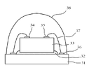
- a light emitting device using a light emitting diode (LED) element is widely used, and the structure of an old type light emitting device is such that, as shown in FIG. 3, an LED element 33 is bonded to a substrate 31 with a die bond adhesive 32, The p electrode 34 and the n electrode 35 on the upper surface are wire-bonded to the connection terminal 36 of the substrate 31 with a gold wire 37, and the entire LED element 33 is sealed with a transparent mold resin 38.
- the gold wire 37 absorbs light having a wavelength of 400 to 500 nm emitted from the LED element 33 to the upper surface side, and a part of the light emitted to the lower surface side. Is absorbed by the die-bonding adhesive 32 and the luminous efficiency of the LED element 33 is reduced.
- the LED element 33 be flip-chip mounted (Patent Document 1).
- bumps 39 are formed on the p electrode 34 and the n electrode 35, respectively, and further, the bump formation surface of the LED element 33 is insulated from the p electrode 34 and the n electrode 35.
- the light reflecting layer 40 is provided on the surface.
- the LED element 33 and the substrate 31 are connected and fixed using an anisotropic conductive paste 41. For this reason, in the light emitting device of FIG. 4, the light emitted upward of the LED element 33 is not absorbed by the gold wire, and most of the light emitted downward is reflected by the light reflecting layer 40 and emitted upward. The luminous efficiency does not decrease.
- the light reflecting layer 40 must be provided on the LED element 33 by a metal vapor deposition method or the like so as to be insulated from the p-electrode 34 and the n-electrode 35, and thus an increase in manufacturing cost is inevitable. There was a problem.
- An object of the present invention is to solve the above-mentioned problems of the prior art, and light reflection that causes an increase in manufacturing cost when a light emitting device using a light emitting diode (LED) element is flip-chip mounted.
- An object is to provide an anisotropic conductive film that does not reduce luminous efficiency without providing a layer on an LED element, and a light-emitting device using the same.
- the present inventor can achieve the above-mentioned object by providing the anisotropic conductive film with a light reflection function.
- the anisotropic conductive film has a two-layer configuration, and one of them is a light-reflective insulating adhesive layer. And the other was an anisotropic conductive adhesive layer, and the present invention was completed.
- the present invention is an anisotropic conductive film in which a light-reflective insulating adhesive layer and an anisotropic conductive adhesive layer are laminated, and the light-reflective insulating adhesive layer is light-transmitted in an insulating adhesive.
- An anisotropic conductive film in which reflective particles are dispersed is provided.
- the present invention also provides a light emitting device in which the substrate and the light emitting diode element are flip-chip mounted via an anisotropic conductive film between a connection terminal on the substrate and a bump for connecting the light emitting diode element. Because The anisotropic conductive film is formed by laminating a light-reflective insulating adhesive layer and an anisotropic conductive adhesive layer, and the light-reflective insulating adhesive layer has light-reflective particles dispersed in the insulating adhesive. A light emitting device which is an anisotropic conductive film is provided.
- the anisotropic conductive film of the present invention has a structure in which a light-reflective insulating adhesive layer and an anisotropic conductive adhesive layer are laminated. Therefore, in the light emitting device manufactured by anisotropically connecting the LED element and the substrate using the LED element, the light emitted from the LED element is directed toward the substrate side (that is, the back side of the LED element). The emitted light is reflected by the light reflective insulating adhesive layer and emitted from the surface side. Therefore, the light emission efficiency of the light emitting device does not decrease.
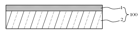
- FIG. 1 is a cross-sectional view of the anisotropic conductive film 100 of the present invention.
- the anisotropic conductive film 100 has a structure in which a light reflective insulating adhesive layer 1 and an anisotropic conductive adhesive layer 2 are laminated, and the light reflective insulating adhesive layer 1 is formed in an insulating adhesive.
- the light reflective particles are dispersed. Therefore, the light incident on the anisotropic conductive film 100 from the light-reflective insulating adhesive layer 1 side is reflected on the incident side, depending on the properties of the light-reflective particles.
- the anisotropic conductive adhesive layer 2 Even if a part of the light incident from the anisotropic conductive adhesive layer 2 is absorbed or scattered by the anisotropic conductive adhesive layer 2, most of the light is reflected by the light-reflective insulating adhesive layer 1 and is anisotropic. Emitted from the conductive conductive adhesive layer 2. Therefore, it is possible to prevent the light emission efficiency of the LED element from being lowered.
- the insulating adhesive constituting the light-reflective insulating adhesive layer 1 those used as insulating binder resins for conventional anisotropic conductive adhesive films can be appropriately employed.
- a thermosetting adhesive in which a crosslinking agent such as an acid anhydride, an imidazole compound, or dicyan can be used in an epoxy resin mainly composed of an alicyclic epoxy resin or a hydrogenated epoxy resin can be used.
- metal oxide particles such as calcium carbonate, titanium dioxide, silicon dioxide, and aluminum oxide
- metal particles such as nickel, silver, and aluminum coated with an insulating film
- the shape of the particles include an amorphous shape, a spherical shape, a scaly shape, and a needle shape.
- a spherical shape is preferable from the viewpoint of the light diffusion effect and a scaly shape is preferable from the viewpoint of the total reflection effect.
- Particularly preferred are scaly silver particles in terms of light reflectance.
- the size of the light-reflective particles varies depending on the shape, but generally, if it is too large, there is a risk of inhibiting connection by anisotropic conductive particles, and if it is too small, it is difficult to reflect light.
- the major axis is preferably 0.1 to 100 ⁇ m, more preferably 1 to 50 ⁇ m, and the thickness is preferably 0. 0.01 to 10 ⁇ m, more preferably 0.1 to 5 ⁇ m.
- the size of the light-reflective particles is the size including the insulating coating when the insulating coating is applied.
- the layer thickness of the light-reflective insulating adhesive layer 1 is preferable from the viewpoint of connection reliability as long as the intended light reflectivity can be obtained. Usually, it is 2 to 30 ⁇ m. Assuming this thickness range, the blending ratio of the insulating adhesive and the light reflective particles in the light reflective insulating adhesive layer 1 varies depending on the shape of the light reflective particles, but the amount is 100 parts by weight of the insulating adhesive. On the other hand, when the light reflective particles are scale-like, the light reflective particles are preferably 1 to 200 parts by mass, more preferably 10 to 100 parts by mass.
- insulating resins can be used as the insulating coating in the metal particles in which the light reflecting particles are coated with an insulating coating.
- a cured product of acrylic resin can be preferably used.
- a preferable example is a resin film obtained by radical copolymerization of methyl methacrylate and 2-hydroxyethyl methacrylate in the presence of a radical initiator such as an organic peroxide such as benzoyl peroxide.
- a radical initiator such as an organic peroxide such as benzoyl peroxide.
- it is more preferably crosslinked with an isocyanate-based crosslinking agent such as 2,4-tolylene diisocyanate.
- the metal oxide particles are also preferably coated with an insulating coating similar to the metal particles from the viewpoint of dispersion stability.
- metal particles it is preferable to introduce a ⁇ -glycidoxy group, a vinyl group or the like into the metal surface in advance with a silane coupling agent.
- anisotropic conductive adhesive layer 2 constituting the anisotropic conductive film 100 of the present invention one having the same configuration as that of a conventional anisotropic conductive film can be used.
- Conductive particles for anisotropic conductive connection are dispersed.
- a thermosetting adhesive for example, an epoxy resin mainly composed of an alicyclic epoxy resin, a hydrogenated epoxy resin, or the like contains a crosslinking agent such as an acid anhydride, an imidazole compound, or dicyan. Things can be mentioned.
- metal particles such as gold and nickel
- metal-coated resin particles in which the surface of resin particles such as benzogranamine resin is coated with a metal such as nickel may be used. it can.
- Such conductive particles have a spherical shape, and if the particle size is too large, the connection reliability is lowered. Therefore, it is preferably 1 to 20 ⁇ m, more preferably 3 to 10 ⁇ m.
- the layer thickness of the anisotropic conductive adhesive layer 2 is usually 5 to 40 ⁇ m in order to obtain the intended connection reliability. Assuming this thickness range, the blending ratio of the insulating adhesive and the conductive particles in the anisotropic conductive adhesive layer 2 is preferably 1 to 50 parts by weight of the conductive particles with respect to 100 parts by weight of the insulating adhesive. More preferably, it is 10 to 25 parts by mass.
- the anisotropic conductive film of the present invention can be manufactured as described below. First, light-reflective particles and an insulating adhesive are dispersed and mixed with a solvent such as toluene, applied to a peeled PET film so as to have a desired thickness, dried at a temperature of about 80 ° C. Create a reflective insulating adhesive layer film. Separately, conductive particles for anisotropic conductive connection and an insulating adhesive are dispersed and mixed together with a solvent such as toluene, and applied to a peeled PET film so as to have a desired thickness, about 80 ° C. An anisotropic conductive adhesive layer film is prepared by drying at the temperature of Next, the anisotropic conductive film of the present invention can be obtained by superimposing the two films and integrating the films by pressing at about 40 ° C. through the release films on both sides.
- the light emitting device 200 includes the anisotropy of the present invention described above between the connection terminal 22 on the substrate 21 and the connection bump 26 formed on each of the n electrode 24 and the p electrode 25 of the LED element 23.
- the substrate 21 and the LED element 23 are flip-chip mounted via a conductive film 100. That is, the anisotropic conductive film 100 is a laminated structure of the light-reflective insulating adhesive layer 1 and the anisotropic conductive adhesive layer 2, and the light-reflective insulating adhesive layer 1 is light-reflective in the insulating adhesive. It is made by dispersing conductive particles.
- the light-reflective insulating adhesive layer 1 of the anisotropic conductive film 100 is desirably disposed on the LED element 23 side, but may be disposed on the opposite side. In addition, you may seal with transparent mold resin so that the whole LED element 23 may be covered as needed.
- the light emitting device 200 configured as described above, light emitted from the LED element 23 toward the substrate 21 is reflected by the light reflective insulating adhesive layer 1 of the anisotropic conductive film 100. Then, the light is emitted from the upper surface of the LED element 23. Accordingly, it is possible to prevent a decrease in luminous efficiency.
- the configuration (the LED element 23, the bump 26, the substrate 21, the connection terminal 22, and the like) can be the same as the configuration of the conventional light emitting device.
- the light emitting device 200 of the present invention can be manufactured using a conventional anisotropic conductive connection technique except that the anisotropic conductive film 100 is used.
- Example 1 (1a) Preparation of light-reflective particles 5 g of scaly silver particles (length 10 ⁇ m, width 10 ⁇ m, thickness 0.5 ⁇ m) and 50 ml of toluene are placed in a flask equipped with a stirrer, and a silane coupling agent (3 0.25 g of (methacryloxypropyltriethoxysilane) was added and stirred at 25 ° C. for 60 minutes. Next, 2 g of methyl methacrylate, 2 g of 2-hydroxyethyl methacrylate, 0.04 g of benzoyl peroxide and 1 g of 2,4-tolylene diisocyanate were added to this mixture and stirred at 80 ° C. for 12 hours. Insulating coated flaky silver particles were obtained as light reflecting particles. The average size of the light-reflective particles including the insulating coating was 10 ⁇ m in length, 10 ⁇ m in width, and 0.5 ⁇ m in thickness.
- anisotropic conductive adhesive layer film 100 parts by mass of the same insulating binder resin as (1b) described above and 20 parts by mass of silver-plated coating resin particles (particle size 5 ⁇ m) were dispersed and mixed in 100 ml of toluene. And the anisotropic conductive adhesive layer film was obtained by apply
- PET polyethylene terephthalate
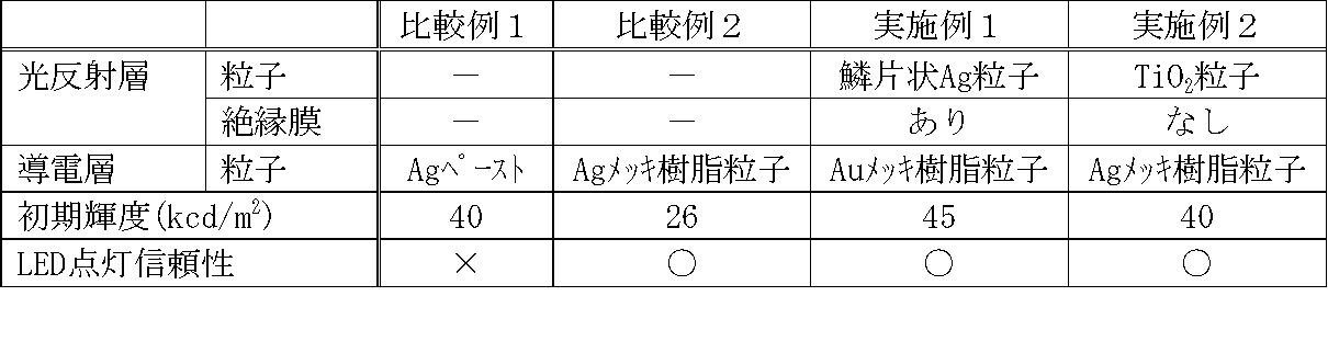
- the obtained light-emitting device was allowed to emit light, and the initial luminance (kcd / m 2 ) of light emitted from the upper surface was measured using a luminance meter (BM-9, Topcon Technohouse Co., Ltd.). Further, the LED lighting reliability is set to “ ⁇ ” when a constant current of 20 mA is passed through the LED at 100 ° C. and the change in Vf value is within ⁇ 0.3V, and the change in Vf value is ⁇ 0.3V. The case of exceeding was evaluated as “ ⁇ ”. The obtained results are shown in Table 1.
- Example 2 In the same manner as in Example 1, except that 50 parts by mass of titanium dioxide particles having an average particle diameter of 0.2 ⁇ m (JR405, Taca Co., Ltd.) were used as the light-reflecting particles instead of the insulating coated scaly silver particles. A conductive insulating adhesive layer film and an anisotropic conductive adhesive layer film were prepared, and further an anisotropic conductive film was prepared. Using this anisotropic conductive film, a light emitting diode element was connected to a glass epoxy substrate in the same manner as in Example 1, and the characteristics were evaluated. The obtained results are shown in Table 1.
- Comparative Example 1 A silver paste was used in place of the anisotropic conductive film, the light emitting diode was connected to a glass epoxy substrate, and the characteristics were evaluated in the same manner as in Example 1. The obtained results are shown in Table 1.
- Example 2 Without using the light-reflective insulating adhesive layer film, the anisotropic conductive adhesive layer film of Example 1 itself was used as the anisotropic conductive film, and the light-emitting diode element was made into a glass epoxy substrate as in Example 1. And was evaluated for characteristics. The obtained results are shown in Table 1.
- Example 1 As can be seen from Table 1, in the case of Example 1, since the scaly Ag particles coated with insulation were used, the initial luminance was higher than that of the silver paste (Comparative Example 1), and the LED lighting reliability was also high. It was good. Further, in Example 2, the use of the TiO 2 particles, indicates the initial luminance comparable to a silver paste (Comparative Example 1), yet was LED lighting reliability satisfactory. In the case of Comparative Example 2, there was a problem in the initial luminance because the light reflecting layer was not provided.
- the anisotropic conductive film of the present invention has a structure in which a light-reflective insulating adhesive layer and an anisotropic conductive adhesive layer are laminated. For this reason, in the light emitting device manufactured by anisotropically connecting the LED element and the substrate using the LED element, the light emitted from the LED element is directed toward the substrate side (that is, the back side of the LED element). The light emitted in this manner can be reflected by the light reflective insulating adhesive layer and emitted from the surface side. Therefore, the light emission efficiency of the light emitting device can be prevented from being lowered. Therefore, the anisotropic conductive film of the present invention is useful when LED elements are flip-lip mounted.
Landscapes
- Chemical & Material Sciences (AREA)
- Organic Chemistry (AREA)
- Engineering & Computer Science (AREA)
- Inorganic Chemistry (AREA)
- Manufacturing & Machinery (AREA)
- Microelectronics & Electronic Packaging (AREA)
- Led Device Packages (AREA)
- Laminated Bodies (AREA)
- Adhesives Or Adhesive Processes (AREA)
- Wire Bonding (AREA)
Abstract
Description
該異方性導電フィルムが、光反射性絶縁接着層と異方性導電接着層とが積層されてなり、該光反射性絶縁接着層が、絶縁性接着剤中に光反射性粒子が分散してなる異方性導電フィルムである発光装置を提供する。
(1a)光反射性粒子の作成
撹拌機つきフラスコに鱗片状銀粒子(縦10μm、横10μm、厚0.5μm)5gとトルエン50mlとを投入し、撹拌しながらフラスコにシランカップリング剤(3-メタクリロキシプロピルトリエトキシシラン)0.25gを投入し、25℃で60分間撹拌した。次に、この混合物に、メタクリル酸メチル2gとメタクリル酸-2-ヒドロキシエチル2gとベンゾイルパーオキサイド0.04gと2,4-トリレンジイソシアネート1gとを投入し、80℃で12時間撹拌することにより、光反射性粒子として絶縁被覆鱗片状銀粒子を得た。絶縁被覆を含めた光反射性粒子の平均的大きさは、縦10μm、横10μm、厚み0.5μmであった。
水添化エポキシ樹脂(YX8000、JER(株))に酸無水物(MH-700、新日本理化(株))、イミダゾール(2MZA、四国化成(株))を加えたことにより絶縁性バインダー樹脂を調製した。得られた絶縁性バインダー樹脂100質量部と絶縁被覆鱗片状銀粒子50質量部とを、トルエン100mlに分散混合し、得られた混合物を、剥離ポリエチレンテレフタレート(PET)フィルムに、乾燥厚で10μmとなるように塗布し、80℃で5分間乾燥することにより、光反射性絶縁性接着層フィルムを得た。
前述の(1b)と同様の絶縁性バインダー樹脂100質量部と銀メッキ被覆樹脂粒子(粒径5μm)20質量部とを、トルエンを100mlに分散混合し、得られた混合物を、剥離ポリエチレンテレフタレート(PET)フィルムに、乾燥厚で10μmとなるように塗布し、80℃で5分間乾燥することにより、異方性導電接着層フィルムを得た。
得られた光反射性絶縁性接着層フィルムと異方性導電接着層フィルムとを重ね合わせ、両側のPETフィルムを介して、40℃で10秒間加圧することにより、両フィルムを積層することにより異方性導電フィルムを得た。
200℃の加熱ヘッドを用い、発光ダイオード素子(If=20mA時の特性が、Vf=3.3V、光度=150mcd、ドミナント波長=470nmである)を、異方性導電フィルムを介しガラスエポキシ基板に1Kg/チップで20秒間加熱加圧することにより接着した。この際、発光ダイオード素子のバンプ部分には圧力がかかるため、光反射性絶縁接着層フィルムの接着剤は排除され、異方性導電接着層の導電粒子で発光ダイオード素子とガラスエポキシ基板との間の導通をとることができた。なお、バンプ以外の光反射性絶縁接着層は排除されず、光反射機能は維持されていた。
光反射性粒子として、絶縁被覆鱗片状銀粒子に代えて、平均粒径0.2μmの二酸化チタン粒子(JR405、テイカ(株))を50質量部使用する以外は実施例1と同様に光反射性絶縁性接着層フィルム、異方性導電接着層フィルムを作成し、更に、異方性導電フィルムを作成した。この異方性導電フィルムを使用し、実施例1と同様に発光ダイオード素子を、ガラスエポキシ基板に接続し、特性評価を行った。得られた結果を表1に示す。
異方性導電フィルムに代えて銀ペーストを使用して、発光ダイオードをガラスエポキシ基板に接続し、実施例1と同様に特性評価を行った。得られた結果を表1に示す。
光反射性絶縁性接着層フィルムを使用せずに、実施例1の異方性導電接着層フィルムそのものを異方性導電フィルムとして使用し、実施例1と同様に発光ダイオード素子を、ガラスエポキシ基板に接続し、特性評価を行った。得られた結果を表1に示す。
2 異方性導電接着層
21 基板
22 接続端子
23 LED素子
24 n電極
25 p電極
26 バンプ
100 異方性導電フィルム
200 発光装置
Claims (7)
- 光反射性絶縁接着層と異方性導電接着層とが積層されてなる異方性導電フィルムであって、該光反射性絶縁接着層が、絶縁性接着剤中に光反射性粒子が分散したものである異方性導電フィルム。
- 光反射性粒子が、絶縁被膜で被覆された金属粒子である請求項1記載の異方性導電フィルム。
- 金属粒子が、鱗片状銀粒子である請求項2記載の異方性導電フィルム。
- 鱗片状金属粒子を被覆する絶縁被膜が、メタクリル酸メチルとメタクリル酸2-ヒドロキシエチルとのラジカル共重合体被膜である請求項2又は3記載の異方性導電フィルム。
- 該絶縁被膜が、イソシアネート系架橋剤で架橋されている請求項4記載の異方性導電フィルム。
- 基板上の接続端子と、発光ダイオード素子の接続用のバンプとの間に異方性導電フィルムを介し、該基板と該発光ダイオード素子とがフリップチップ実装されている発光装置であって、
該異方性導電フィルムが、光反射性絶縁接着層と異方性導電接着層とが積層されてなり、該光反射性絶縁接着層が、絶縁性接着剤中に光反射性粒子が分散してなる異方性導電フィルムである発光装置。 - 該異方性導電フィルムの光反射性絶縁接着層が発光ダイオード素子側に配置されている請求項6記載の発光装置。
Priority Applications (3)
| Application Number | Priority Date | Filing Date | Title |
|---|---|---|---|
| KR1020117016655A KR101695994B1 (ko) | 2009-02-27 | 2010-02-22 | 이방성 도전 필름 및 발광 장치 |
| CN201080009516.2A CN102334238B (zh) | 2009-02-27 | 2010-02-22 | 各向异性导电膜和发光装置 |
| US13/142,956 US8444882B2 (en) | 2009-02-27 | 2010-02-22 | Anisotropic conductive film and light emitting device |
Applications Claiming Priority (4)
| Application Number | Priority Date | Filing Date | Title |
|---|---|---|---|
| JP2009-045337 | 2009-02-27 | ||
| JP2009045337 | 2009-02-27 | ||
| JP2009057316A JP5402109B2 (ja) | 2009-02-27 | 2009-03-11 | 異方性導電フィルム及び発光装置 |
| JP2009-057316 | 2009-03-11 |
Publications (1)
| Publication Number | Publication Date |
|---|---|
| WO2010098273A1 true WO2010098273A1 (ja) | 2010-09-02 |
Family
ID=42665480
Family Applications (1)
| Application Number | Title | Priority Date | Filing Date |
|---|---|---|---|
| PCT/JP2010/052600 Ceased WO2010098273A1 (ja) | 2009-02-27 | 2010-02-22 | 異方性導電フィルム及び発光装置 |
Country Status (6)
| Country | Link |
|---|---|
| US (1) | US8444882B2 (ja) |
| JP (1) | JP5402109B2 (ja) |
| KR (1) | KR101695994B1 (ja) |
| CN (1) | CN102334238B (ja) |
| TW (1) | TWI478180B (ja) |
| WO (1) | WO2010098273A1 (ja) |
Cited By (13)
| Publication number | Priority date | Publication date | Assignee | Title |
|---|---|---|---|---|
| WO2012046539A1 (ja) * | 2010-10-07 | 2012-04-12 | ソニーケミカル&インフォメーションデバイス株式会社 | マルチチップ実装用緩衝フィルム |
| CN102683562A (zh) * | 2011-02-24 | 2012-09-19 | 日东电工株式会社 | 发光二极管元件及发光二极管装置 |
| US8384121B2 (en) | 2010-06-29 | 2013-02-26 | Cooledge Lighting Inc. | Electronic devices with yielding substrates |
| WO2013073563A1 (ja) * | 2011-11-14 | 2013-05-23 | デクセリアルズ株式会社 | 異方性導電フィルム、接続方法、及び接合体 |
| JP2014049642A (ja) * | 2012-08-31 | 2014-03-17 | Nichia Chem Ind Ltd | 発光装置およびその製造方法 |
| EP2637229A4 (en) * | 2010-11-02 | 2014-06-18 | Lg Chemical Ltd | Adhesive film and method for encapsulating an organic electrical device therefor |
| CN104024360A (zh) * | 2012-01-06 | 2014-09-03 | Lg化学株式会社 | 电子装置的制造方法 |
| US8860318B2 (en) | 2010-01-04 | 2014-10-14 | Cooledge Lighting Inc. | Failure mitigation in arrays of light-emitting devices |
| US8877561B2 (en) | 2012-06-07 | 2014-11-04 | Cooledge Lighting Inc. | Methods of fabricating wafer-level flip chip device packages |
| EP2685513A4 (en) * | 2011-03-07 | 2014-12-31 | Dexerials Corp | LIGHT-REFLECTING, ANISOTROPICALLY CONDUCTIVE ADHESIVE AND LIGHT-EMITTING DEVICE |
| US9179510B2 (en) | 2009-06-27 | 2015-11-03 | Cooledge Lighting Inc. | High efficiency LEDs and LED lamps |
| US9480133B2 (en) | 2010-01-04 | 2016-10-25 | Cooledge Lighting Inc. | Light-emitting element repair in array-based lighting devices |
| JP2018129426A (ja) * | 2017-02-09 | 2018-08-16 | 株式会社ディスコ | ウエーハの加工方法及び粘着テープ |
Families Citing this family (29)
| Publication number | Priority date | Publication date | Assignee | Title |
|---|---|---|---|---|
| JP2012080085A (ja) * | 2010-09-10 | 2012-04-19 | Nichia Chem Ind Ltd | 支持体及びそれを用いた発光装置 |
| US8455895B2 (en) * | 2010-11-08 | 2013-06-04 | Bridgelux, Inc. | LED-based light source utilizing asymmetric conductors |
| KR20120082714A (ko) * | 2011-01-14 | 2012-07-24 | 삼성엘이디 주식회사 | 발광소자용 접착필름 및 이를 이용한 발광다이오드 패키지 제조방법 |
| US9269878B2 (en) * | 2011-05-27 | 2016-02-23 | Lg Innotek Co., Ltd. | Light emitting device and light emitting apparatus |
| CN103930501B (zh) * | 2011-11-14 | 2017-09-12 | Lg化学株式会社 | 粘合膜 |
| JP2013143426A (ja) * | 2012-01-10 | 2013-07-22 | Nitto Denko Corp | 導電性接着シートおよび太陽電池モジュール |
| CN102709438A (zh) * | 2012-03-22 | 2012-10-03 | 浙江英特来光电科技有限公司 | 一种大功率陶瓷led无线封装结构 |
| CN103378282A (zh) * | 2012-04-27 | 2013-10-30 | 展晶科技(深圳)有限公司 | 发光二极管封装结构的制造方法 |
| US9337405B2 (en) * | 2012-08-31 | 2016-05-10 | Nichia Corporation | Light emitting device and method for manufacturing the same |
| JP6176910B2 (ja) * | 2012-09-24 | 2017-08-09 | デクセリアルズ株式会社 | 接続構造体の製造方法 |
| CN105009314B (zh) * | 2013-02-27 | 2019-11-05 | 日亚化学工业株式会社 | 发光装置、发光元件安装方法以及发光元件用安装装置 |
| KR101513641B1 (ko) * | 2013-08-20 | 2015-04-22 | 엘지전자 주식회사 | 표시장치 |
| US9954144B2 (en) * | 2014-01-10 | 2018-04-24 | Cree, Inc. | Wafer level contact pad solder bumping for surface mount devices with non-planar recessed contacting surfaces |
| JP6349910B2 (ja) * | 2014-04-23 | 2018-07-04 | 日亜化学工業株式会社 | 発光装置及びその製造方法 |
| CN103881603B (zh) * | 2014-04-14 | 2015-07-29 | 苏州斯迪克新材料科技股份有限公司 | 一种异向导电胶带的制备方法 |
| JP6484983B2 (ja) * | 2014-09-30 | 2019-03-20 | 日亜化学工業株式会社 | 発光装置およびその製造方法 |
| JP5925928B1 (ja) * | 2015-02-26 | 2016-05-25 | 日本航空電子工業株式会社 | 電気接続構造および電気接続部材 |
| US10062660B2 (en) | 2015-03-04 | 2018-08-28 | Trillion Science, Inc. | Anisotropic conductive film including a reflective layer |
| US9871177B2 (en) * | 2015-03-04 | 2018-01-16 | Trillion Science, Inc. | Anisotropic conductive film (ACF) including a relfective layer |
| DE102015112967A1 (de) * | 2015-08-06 | 2017-02-09 | Osram Opto Semiconductors Gmbh | Verfahren zum Herstellen eines optoelektronischen Bauelements und optoelektronisches Bauelement |
| DE102015120642A1 (de) | 2015-11-27 | 2017-06-01 | Osram Opto Semiconductors Gmbh | Vorrichtung mit zumindest einem optoelektronischen Halbleiterbauelement |
| KR102446768B1 (ko) | 2015-12-14 | 2022-09-23 | 엘지전자 주식회사 | 반도체 발광 소자를 이용한 디스플레이 장치 및 이의 제조방법 |
| TWI696300B (zh) | 2016-03-15 | 2020-06-11 | 晶元光電股份有限公司 | 半導體裝置及其製造方法 |
| JP6729258B2 (ja) * | 2016-09-30 | 2020-07-22 | ブラザー工業株式会社 | 粘着テープカートリッジ及び粘着テープロールの製造方法 |
| CN108267914B (zh) * | 2016-12-30 | 2022-01-11 | 中强光电股份有限公司 | 波长转换装置及其投影机 |
| CN113875320B (zh) * | 2019-05-23 | 2025-05-27 | 昕诺飞控股有限公司 | 针对固态光源应用的稳定pcb |
| KR102862766B1 (ko) * | 2019-05-29 | 2025-09-22 | 삼성전자주식회사 | 마이크로 엘이디 디스플레이 및 이의 제작 방법 |
| KR102781957B1 (ko) | 2020-07-07 | 2025-03-18 | 삼성전자주식회사 | 디스플레이 모듈 및 그 제조 방법 |
| WO2022067506A1 (zh) * | 2020-09-29 | 2022-04-07 | 重庆康佳光电技术研究院有限公司 | 显示面板及其制作方法 |
Citations (4)
| Publication number | Priority date | Publication date | Assignee | Title |
|---|---|---|---|---|
| JPH0792305A (ja) * | 1993-09-24 | 1995-04-07 | Dainippon Printing Co Ltd | 低屈折率反射防止膜、反射防止フィルムおよびその製造方法 |
| JP2002270641A (ja) * | 2001-03-12 | 2002-09-20 | Asahi Kasei Corp | ベアチップ用異方導電性フィルム |
| JP2005159263A (ja) * | 2003-10-30 | 2005-06-16 | Kyocera Corp | 発光装置および照明装置 |
| WO2008020482A1 (fr) * | 2006-08-18 | 2008-02-21 | Reiko Co., Ltd. | Matière isolante qui excelle par son brillant métallique et article moulé qui utilise celle-ci |
Family Cites Families (11)
| Publication number | Priority date | Publication date | Assignee | Title |
|---|---|---|---|---|
| JPH07326476A (ja) * | 1994-05-31 | 1995-12-12 | Nec Kansai Ltd | 電界発光灯およびその製造方法 |
| JPH11168235A (ja) * | 1997-12-05 | 1999-06-22 | Toyoda Gosei Co Ltd | 発光ダイオード |
| JPH11320962A (ja) * | 1998-05-19 | 1999-11-24 | Canon Inc | Led露光ヘッド |
| JP3491595B2 (ja) * | 2000-02-25 | 2004-01-26 | ソニーケミカル株式会社 | 異方導電性接着フィルム |
| JP4222017B2 (ja) * | 2001-12-18 | 2009-02-12 | 日亜化学工業株式会社 | 発光装置 |
| US20050133808A1 (en) | 2003-09-11 | 2005-06-23 | Kyocera Corporation | Package for housing light-emitting element, light-emitting apparatus and illumination apparatus |
| TWI245436B (en) * | 2003-10-30 | 2005-12-11 | Kyocera Corp | Package for housing light-emitting element, light-emitting apparatus and illumination apparatus |
| JP4385794B2 (ja) * | 2004-02-26 | 2009-12-16 | ソニーケミカル&インフォメーションデバイス株式会社 | 異方性導電接続方法 |
| KR20070042615A (ko) * | 2005-10-19 | 2007-04-24 | 삼성전자주식회사 | 어레이 기판 및 이의 제조방법 |
| JP5617210B2 (ja) * | 2009-09-14 | 2014-11-05 | デクセリアルズ株式会社 | 光反射性異方性導電接着剤及び発光装置 |
| KR101829475B1 (ko) * | 2010-06-09 | 2018-02-14 | 데쿠세리아루즈 가부시키가이샤 | 광반사성 이방성 도전 페이스트 및 발광 장치 |
-
2009
- 2009-03-11 JP JP2009057316A patent/JP5402109B2/ja not_active Expired - Fee Related
-
2010
- 2010-02-22 CN CN201080009516.2A patent/CN102334238B/zh not_active Expired - Fee Related
- 2010-02-22 US US13/142,956 patent/US8444882B2/en not_active Expired - Fee Related
- 2010-02-22 KR KR1020117016655A patent/KR101695994B1/ko active Active
- 2010-02-22 WO PCT/JP2010/052600 patent/WO2010098273A1/ja not_active Ceased
- 2010-02-26 TW TW099105550A patent/TWI478180B/zh not_active IP Right Cessation
Patent Citations (4)
| Publication number | Priority date | Publication date | Assignee | Title |
|---|---|---|---|---|
| JPH0792305A (ja) * | 1993-09-24 | 1995-04-07 | Dainippon Printing Co Ltd | 低屈折率反射防止膜、反射防止フィルムおよびその製造方法 |
| JP2002270641A (ja) * | 2001-03-12 | 2002-09-20 | Asahi Kasei Corp | ベアチップ用異方導電性フィルム |
| JP2005159263A (ja) * | 2003-10-30 | 2005-06-16 | Kyocera Corp | 発光装置および照明装置 |
| WO2008020482A1 (fr) * | 2006-08-18 | 2008-02-21 | Reiko Co., Ltd. | Matière isolante qui excelle par son brillant métallique et article moulé qui utilise celle-ci |
Cited By (42)
| Publication number | Priority date | Publication date | Assignee | Title |
|---|---|---|---|---|
| US9559150B2 (en) | 2009-06-27 | 2017-01-31 | Cooledge Lighting Inc. | High efficiency LEDs and LED lamps |
| US11415272B2 (en) | 2009-06-27 | 2022-08-16 | Cooledge Lighting, Inc. | High efficiency LEDs and LED lamps |
| US10910522B2 (en) | 2009-06-27 | 2021-02-02 | Cooledge Lighting Inc. | High efficiency LEDs and LED lamps |
| US9179510B2 (en) | 2009-06-27 | 2015-11-03 | Cooledge Lighting Inc. | High efficiency LEDs and LED lamps |
| US10281091B2 (en) | 2009-06-27 | 2019-05-07 | Cooledge Lighting Inc. | High efficiency LEDs and LED lamps |
| US9966414B2 (en) | 2009-06-27 | 2018-05-08 | Cooledge Lighting Inc. | High efficiency LEDs and LED lamps |
| US9431462B2 (en) | 2009-06-27 | 2016-08-30 | Cooledge Lighting, Inc. | High efficiency LEDs and LED lamps |
| US9765936B2 (en) | 2009-06-27 | 2017-09-19 | Cooledge Lighting Inc. | High efficiency LEDs and LED lamps |
| US8860318B2 (en) | 2010-01-04 | 2014-10-14 | Cooledge Lighting Inc. | Failure mitigation in arrays of light-emitting devices |
| US9480133B2 (en) | 2010-01-04 | 2016-10-25 | Cooledge Lighting Inc. | Light-emitting element repair in array-based lighting devices |
| US9107272B2 (en) | 2010-01-04 | 2015-08-11 | Cooledge Lighting Inc. | Failure mitigation in arrays of light-emitting devices |
| US8680567B2 (en) | 2010-06-29 | 2014-03-25 | Cooledge Lighting Inc. | Electronic devices with yielding substrates |
| US8466488B2 (en) | 2010-06-29 | 2013-06-18 | Cooledge Lighting Inc. | Electronic devices with yielding substrates |
| US9426860B2 (en) | 2010-06-29 | 2016-08-23 | Cooledge Lighting, Inc. | Electronic devices with yielding substrates |
| US8907370B2 (en) | 2010-06-29 | 2014-12-09 | Cooledge Lighting Inc. | Electronic devices with yielding substrates |
| US9252373B2 (en) | 2010-06-29 | 2016-02-02 | Cooledge Lighting, Inc. | Electronic devices with yielding substrates |
| US8384121B2 (en) | 2010-06-29 | 2013-02-26 | Cooledge Lighting Inc. | Electronic devices with yielding substrates |
| US9054290B2 (en) | 2010-06-29 | 2015-06-09 | Cooledge Lighting Inc. | Electronic devices with yielding substrates |
| US8758546B2 (en) | 2010-10-07 | 2014-06-24 | Dexerials Corporation | Buffer film for multi-chip packaging |
| WO2012046539A1 (ja) * | 2010-10-07 | 2012-04-12 | ソニーケミカル&インフォメーションデバイス株式会社 | マルチチップ実装用緩衝フィルム |
| JP2012084582A (ja) * | 2010-10-07 | 2012-04-26 | Sony Chemical & Information Device Corp | マルチチップ実装用緩衝フィルム |
| EP2637229A4 (en) * | 2010-11-02 | 2014-06-18 | Lg Chemical Ltd | Adhesive film and method for encapsulating an organic electrical device therefor |
| CN104882564A (zh) * | 2010-11-02 | 2015-09-02 | Lg化学株式会社 | 粘合膜和使用其包封有机电子装置的方法 |
| CN104221178A (zh) * | 2010-11-02 | 2014-12-17 | Lg化学株式会社 | 粘合膜和使用其包封有机电子装置的方法 |
| CN110951410B (zh) * | 2010-11-02 | 2022-05-31 | Lg化学株式会社 | 粘合膜和使用其包封有机电子装置的方法 |
| US11142669B2 (en) | 2010-11-02 | 2021-10-12 | Lg Chem, Ltd. | Adhesive and method of encapsulating organic electronic device using the same |
| US9105648B2 (en) | 2010-11-02 | 2015-08-11 | Lg Chem, Ltd. | Adhesive and method of encapsulating organic electronic device using the same |
| US10622573B2 (en) | 2010-11-02 | 2020-04-14 | Lg Chem, Ltd. | Adhesive and method of encapsulating organic electronic device using the same |
| CN110951410A (zh) * | 2010-11-02 | 2020-04-03 | Lg化学株式会社 | 粘合膜和使用其包封有机电子装置的方法 |
| US10062855B2 (en) | 2010-11-02 | 2018-08-28 | Lg Chem, Ltd. | Adhesive and method of encapsulating organic electronic device using the same |
| CN102683562A (zh) * | 2011-02-24 | 2012-09-19 | 日东电工株式会社 | 发光二极管元件及发光二极管装置 |
| EP2685513A4 (en) * | 2011-03-07 | 2014-12-31 | Dexerials Corp | LIGHT-REFLECTING, ANISOTROPICALLY CONDUCTIVE ADHESIVE AND LIGHT-EMITTING DEVICE |
| WO2013073563A1 (ja) * | 2011-11-14 | 2013-05-23 | デクセリアルズ株式会社 | 異方性導電フィルム、接続方法、及び接合体 |
| JP2013105636A (ja) * | 2011-11-14 | 2013-05-30 | Dexerials Corp | 異方性導電フィルム、接続方法、及び接合体 |
| CN104024360B (zh) * | 2012-01-06 | 2016-09-07 | Lg化学株式会社 | 电子装置的制造方法 |
| US10141543B2 (en) | 2012-01-06 | 2018-11-27 | Lg Chem, Ltd. | Method for manufacturing electronic device |
| CN104024360A (zh) * | 2012-01-06 | 2014-09-03 | Lg化学株式会社 | 电子装置的制造方法 |
| US9214615B2 (en) | 2012-06-07 | 2015-12-15 | Cooledge Lighting Inc. | Methods of fabricating wafer-level flip chip device packages |
| US8877561B2 (en) | 2012-06-07 | 2014-11-04 | Cooledge Lighting Inc. | Methods of fabricating wafer-level flip chip device packages |
| US9231178B2 (en) | 2012-06-07 | 2016-01-05 | Cooledge Lighting, Inc. | Wafer-level flip chip device packages and related methods |
| JP2014049642A (ja) * | 2012-08-31 | 2014-03-17 | Nichia Chem Ind Ltd | 発光装置およびその製造方法 |
| JP2018129426A (ja) * | 2017-02-09 | 2018-08-16 | 株式会社ディスコ | ウエーハの加工方法及び粘着テープ |
Also Published As
| Publication number | Publication date |
|---|---|
| TWI478180B (zh) | 2015-03-21 |
| JP2010225597A (ja) | 2010-10-07 |
| KR101695994B1 (ko) | 2017-01-13 |
| US20110266578A1 (en) | 2011-11-03 |
| CN102334238B (zh) | 2016-03-30 |
| JP5402109B2 (ja) | 2014-01-29 |
| TW201032241A (en) | 2010-09-01 |
| KR20110126104A (ko) | 2011-11-22 |
| CN102334238A (zh) | 2012-01-25 |
| US8444882B2 (en) | 2013-05-21 |
Similar Documents
| Publication | Publication Date | Title |
|---|---|---|
| JP5402109B2 (ja) | 異方性導電フィルム及び発光装置 | |
| CN103403896B (zh) | 光反射性各向异性导电粘接剂以及发光装置 | |
| JP5617210B2 (ja) | 光反射性異方性導電接着剤及び発光装置 | |
| CN102934243B (zh) | 光反射性各向异性导电浆料和发光装置 | |
| TWI534839B (zh) | Light reflective conductive particles, anisotropic conductive adhesives and light-emitting devices | |
| JP5555038B2 (ja) | 光反射性異方性導電接着剤及び発光装置 | |
| US9670384B2 (en) | Light-reflective anisotropic conductive adhesive and light-emitting device | |
| TWI517456B (zh) | Light reflective conductive particles, anisotropic conductive adhesives and light-emitting devices | |
| JP5785306B2 (ja) | 光反射性異方性導電接着剤及び発光装置 | |
| JP2014030026A (ja) | 異方性導電接着剤及び発光装置 | |
| HK1178320B (en) | Light-reflective anisotropic conductive adhesive agent, and light emitting device | |
| HK1170255B (en) | Light-reflective anisotropic electroconductive adhesive agent and light-emitting device | |
| HK1191450A (en) | Light-reflective anisotropic conductive adhesive and light-emitting device | |
| HK1191450B (en) | Light-reflective anisotropic conductive adhesive and light-emitting device |
Legal Events
| Date | Code | Title | Description |
|---|---|---|---|
| WWE | Wipo information: entry into national phase |
Ref document number: 201080009516.2 Country of ref document: CN |
|
| 121 | Ep: the epo has been informed by wipo that ep was designated in this application |
Ref document number: 10746154 Country of ref document: EP Kind code of ref document: A1 |
|
| DPE1 | Request for preliminary examination filed after expiration of 19th month from priority date (pct application filed from 20040101) | ||
| WWE | Wipo information: entry into national phase |
Ref document number: 13142956 Country of ref document: US |
|
| ENP | Entry into the national phase |
Ref document number: 20117016655 Country of ref document: KR Kind code of ref document: A |
|
| NENP | Non-entry into the national phase |
Ref country code: DE |
|
| 122 | Ep: pct application non-entry in european phase |
Ref document number: 10746154 Country of ref document: EP Kind code of ref document: A1 |