WO2010090152A1 - 半導体欠陥統合投影方法および半導体欠陥統合投影機能を実装した欠陥検査支援装置 - Google Patents
半導体欠陥統合投影方法および半導体欠陥統合投影機能を実装した欠陥検査支援装置 Download PDFInfo
- Publication number
- WO2010090152A1 WO2010090152A1 PCT/JP2010/051319 JP2010051319W WO2010090152A1 WO 2010090152 A1 WO2010090152 A1 WO 2010090152A1 JP 2010051319 W JP2010051319 W JP 2010051319W WO 2010090152 A1 WO2010090152 A1 WO 2010090152A1
- Authority
- WO
- WIPO (PCT)
- Prior art keywords
- defect
- design layout
- information
- design
- layout data
- Prior art date
- Legal status (The legal status is an assumption and is not a legal conclusion. Google has not performed a legal analysis and makes no representation as to the accuracy of the status listed.)
- Ceased
Links
Images





Classifications
-
- H—ELECTRICITY
- H10—SEMICONDUCTOR DEVICES; ELECTRIC SOLID-STATE DEVICES NOT OTHERWISE PROVIDED FOR
- H10P—GENERIC PROCESSES OR APPARATUS FOR THE MANUFACTURE OR TREATMENT OF DEVICES COVERED BY CLASS H10
- H10P74/00—Testing or measuring during manufacture or treatment of wafers, substrates or devices
-
- G—PHYSICS
- G06—COMPUTING OR CALCULATING; COUNTING
- G06T—IMAGE DATA PROCESSING OR GENERATION, IN GENERAL
- G06T7/00—Image analysis
- G06T7/0002—Inspection of images, e.g. flaw detection
- G06T7/0004—Industrial image inspection
- G06T7/001—Industrial image inspection using an image reference approach
-
- G—PHYSICS
- G01—MEASURING; TESTING
- G01N—INVESTIGATING OR ANALYSING MATERIALS BY DETERMINING THEIR CHEMICAL OR PHYSICAL PROPERTIES
- G01N21/00—Investigating or analysing materials by the use of optical means, i.e. using sub-millimetre waves, infrared, visible or ultraviolet light
- G01N21/84—Systems specially adapted for particular applications
- G01N21/88—Investigating the presence of flaws or contamination
- G01N21/95—Investigating the presence of flaws or contamination characterised by the material or shape of the object to be examined
- G01N21/956—Inspecting patterns on the surface of objects
-
- G—PHYSICS
- G06—COMPUTING OR CALCULATING; COUNTING
- G06T—IMAGE DATA PROCESSING OR GENERATION, IN GENERAL
- G06T1/00—General purpose image data processing
-
- H—ELECTRICITY
- H10—SEMICONDUCTOR DEVICES; ELECTRIC SOLID-STATE DEVICES NOT OTHERWISE PROVIDED FOR
- H10P—GENERIC PROCESSES OR APPARATUS FOR THE MANUFACTURE OR TREATMENT OF DEVICES COVERED BY CLASS H10
- H10P74/00—Testing or measuring during manufacture or treatment of wafers, substrates or devices
- H10P74/20—Testing or measuring during manufacture or treatment of wafers, substrates or devices characterised by the properties tested or measured, e.g. structural or electrical properties
- H10P74/203—Structural properties, e.g. testing or measuring thicknesses, line widths, warpage, bond strengths or physical defects
-
- G—PHYSICS
- G06—COMPUTING OR CALCULATING; COUNTING
- G06F—ELECTRIC DIGITAL DATA PROCESSING
- G06F30/00—Computer-aided design [CAD]
- G06F30/30—Circuit design
- G06F30/39—Circuit design at the physical level
-
- G—PHYSICS
- G06—COMPUTING OR CALCULATING; COUNTING
- G06T—IMAGE DATA PROCESSING OR GENERATION, IN GENERAL
- G06T2207/00—Indexing scheme for image analysis or image enhancement
- G06T2207/30—Subject of image; Context of image processing
- G06T2207/30108—Industrial image inspection
- G06T2207/30148—Semiconductor; IC; Wafer
Definitions
- the present invention improves the operability and convenience of each device by processing the data acquired by an inspection device or defect review device in which fine circuit patterns are formed, such as semiconductor devices and liquid crystal devices, and feeding back to each device. It is related to the inspection support technology to make it.
- the presence of defects is detected by comparing circuit patterns of the same type of multiple LSIs using optical images for the purpose of finding foreign matter defects such as foreign matter adhesion and investigating the cause.
- the electron beam image with higher resolution than the optical image by applying the technology of the optical pattern inspection device and the scanning electron microscope (SEM: Scanning Electron Microscope), the same comparison operation processing as the optical pattern inspection device
- SEM Scanning Electron Microscope
- An SEM type pattern inspection apparatus that detects the location of a structural or electrical defect in a circuit pattern is used.
- a defect review apparatus that automatically images the position of a detected defect with high accuracy and automatically executes a classification process for each defect type (ADC: Automatic Defect Classification) has been put into practical use.
- ADC Automatic Defect Classification
- these inspection apparatuses are arranged for each manufacturing process of each layer (hierarchy) constituting a semiconductor device, and detect defects by foreign substance inspection and circuit pattern inspection.
- the detected defect is used as information for determining the quality of the manufacturing process by specifying the type and measuring the number of occurrences for each type.
- a defect distribution image data or a defect distribution grayscale image data created for each manufacturing process is compared.
- an invention is disclosed in which a detected defect is found and a manufacturing process that causes the defect is identified. Then, depending on the detected defect, measures for manufacturing such as changing the design or changing the manufacturing conditions are taken.
- Patent Document 2 compares image information obtained from an optical inspection apparatus with a design pattern of a semiconductor device, and an inspection for determining whether a detected defect is fatal or non-fatal according to the degree of overlap between a defect and a wiring pattern. A method is disclosed. What is really needed as information for determining good or bad manufacturing processes is the number of fatal defects, and from the viewpoint of improving inspection speed, the inspection equipment should detect only fatal defects without detecting non-fatal defects. In many cases, this function is required.
- Patent Document 3 discloses an invention related to an EB tester that designates an irradiation position of an electron beam on a design pattern.
- the EB tester is an inspection device for irradiating a completed chip on a wafer with an electron beam to test whether it operates as a circuit.
- the image displayed on the GUI is not the image of the wiring pattern to be inspected, but the protective film pattern on the wiring pattern.
- the present invention has been made in view of the above problems, and displays information relating to defects found by the inspection apparatus or defects by the inspection review apparatus in an integrated manner with the design layout data, enabling analysis, and resulting from the design layout data.
- a means for efficiently determining the cause of the problem is provided.
- the present invention utilizes semiconductor design layout data and integrally projects defects on a chip basis onto the design layout data.
- the image captured by the defect review device at the time of defect detection and the corresponding design layout data and arbitrary design layout data are simultaneously integrated and projected, and the lower and upper circuit patterns are displayed and displayed. By switching, the analysis of the defective part is supported.
- the semiconductor inspection support apparatus of the present invention includes a design layout data reading unit that acquires design layout data including position information of a design circuit pattern used in each process of semiconductor manufacturing, and a plurality of the design circuit patterns are formed for each chip.
- Wafer / chip information reading unit for acquiring wafer / chip information including at least design cell position information from the data relating to the processed wafer, and defect data for acquiring defect data including position information of defects generated in each process
- the design layout data and the defect data are integrated and projected in the process in which a defect has occurred in the design layout data, thereby integrating the design layout data defects.
- a processing unit characterized in that it comprises a defect integrated projection display device for displaying the design layout data defective integrated projection display view.
- defect information can be examined from a multifaceted and multi-layered basis. As a result, the yield can be improved as useful information for examining defect countermeasures.
- FIG. 2 is an explanation of a semiconductor defect integrated projection system in Embodiment 1.
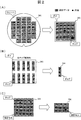
- 5 is a display example of defect integrated projection display in the first embodiment.
- 2A is a display example of die defect integrated projection
- FIG. 2B is a display example of chip defect integrated projection
- FIG. 2C is a display example of design cell defect integrated projection.
- 6 is a display example of integrated projection display of defects and design layout data in the first embodiment.
- 3A is a display example of die defect integrated projection
- FIG. 3B is an example of enlarged display of design layout data of a defective part
- FIG. 3C is an example of enlarged display of arbitrary design layout data
- FIG. 3E is an example of overlapping enlarged display of a captured image and arbitrary design layout data. It is a figure which shows the flowchart of the defect integrated projection means in Embodiment 1.
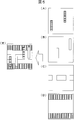
- FIG. It is a conceptual diagram which shows that the pattern of a certain hierarchy is formed by the superimposition of the design pattern of several layers.
- 5A is a design pattern corresponding to the upper layer pattern 2 (dummy pattern)
- FIG. 5B is a design pattern corresponding to the upper layer pattern 1 (active pattern)
- FIG. 5C is an intermediate layer pattern (active pattern).
- FIG. 5D is a design pattern corresponding to the lower layer pattern (active pattern)
- FIG. 5E is formed by superimposing the design patterns of FIGS. 5A to 5D. Hierarchical design pattern.
- FIG. 5A is a design pattern corresponding to the upper layer pattern 2 (dummy pattern)
- FIG. 5B is a design pattern corresponding to the upper layer pattern 1 (active pattern)
- FIG. 5C is an intermediate layer pattern (
- FIG. 10 is a layout diagram illustrating a defect inspection support apparatus according to a second embodiment and the surrounding environment. It is a functional block diagram which implement
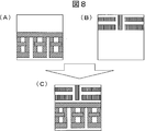
- 8A is a design pattern corresponding to the active pattern
- FIG. 8B is a design pattern corresponding to the dummy pattern
- FIG. 8C is an overlay of the design patterns shown in FIGS. 8A and 8B.
- 9A is an inspection image before synthesis of the defect integrated projection image
- FIG. 9B is a design wiring pattern as a background, and FIG.
- 9C is a defect projection image after the defect-background synthesis processing. . It is a display image before and after the critical defect screening.
- 10A is a defect map showing the entire wafer before the critical defect screening
- FIG. 10B is a defect map showing the entire wafer after the critical defect screening
- FIG. 10C is a critical defect screening.
- FIG. 10D is an enlarged view of a part of the cell after the fatal defect screening.
- FIG. It is a schematic diagram of the defect integrated projection image synthesized using the design layout data of a different hierarchy from the inspection image.
- 11A shows an inspection image
- FIG. 11B shows design layout data of a downstream process
- FIG. 11C shows a defect integrated projection image after the synthesis of FIGS. 11A and 11B.
- FIG. 1 is an illustration of a semiconductor defect integrated projection system showing an embodiment of the present invention.
- the semiconductor defect integrated projection system includes an inspection support apparatus configured by a computer system 1 equipped with a defect integrated projection means 2, a defect integrated instruction information input apparatus 4 for giving an instruction from the user to the defect integrated projection means 2, and design of a semiconductor chip.
- Design data storage device for storing layout data manufacturing process information, mask information, design circuit pattern position information, design cell position information, layer ID (ID Information: Identification Information) that is identification information of a layer to which a design pattern belongs 5. Die position information on the wafer, chip position information, design circuit pattern position information on the chip and design cell position information, wafer ID or chip ID, which is wafer or chip identification information, manufacturing process information, imaging data, etc.
- the design data storage device 5, the wafer data storage device 6, and the defect data storage device 7 may be connected via a network.
- each data may be stored in a portable recording medium and input and processed on a computer system.
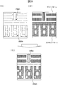
- FIG. 2 shows an example of the defect integrated projection display for projecting the defect display onto the design layout data.
- the defect information and the design layout data are integratedly projected and displayed from a large unit to a small unit in the order of wafer, die, chip, and cell.
- Example of die defect integrated projection display 201 is a diagram in which defect information (black circles) of a plurality of dies arranged on the inspection wafer and design layout data are integratedly projected and displayed.
- 202 is a diagram in which the defect information 201 on the wafer is integrally projected and displayed on a die basis.
- a plurality of semiconductor chips are formed on the die, and the plurality of chips as a whole operate as one semiconductor device.
- 203 is a diagram in which defect information (black circles) and design layout data of a plurality of chips arranged on the die are integratedly projected and displayed.
- defect information on the die is integrally projected and displayed in units of chips in the above-described case.
- Example of design cell defect integrated projection display 205 is a diagram in which defect information (black circles) of a plurality of cells arranged on a chip and design layout data are integrally projected and displayed.
- defect information 205 on the chip is integrated and displayed in units of cells.
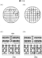
- FIG. 3 shows an enlarged display example of the design layout data defect integrated projection.
- the defect position can be displayed on the screen on the design layout data corresponding to the process at the time of inspection.
- defect information 301 is a diagram in which defect information is integratedly projected and displayed on design layout data in units of dies by the defect integrated projection means 2.
- the defect position is indicated by a black circle.
- the cause / type of the defect cannot be determined only by the design layout data of the process in which the defect is found, it is necessary to examine it by comparing it with arbitrary design layout data.
- the arbitrary design layout data is, for example, design layout data before or after the process in which a defect is found, or the like.
- connection wiring, elements, or the like which are peripheral information of the defective part on the design layout data of a certain process, it is possible to determine the influence and severity of the defective part on the entire chip.
- 303 is a diagram in which the defect portion is enlarged and the design layout data and arbitrary design layout data of the process in which the defect is found are superimposed and displayed. As a result, it is possible to easily determine the cause and type of the defect even if the defect cannot be determined only by the design layout data pattern of the process in which the defect is found.
- the design layout data of a plurality of processes (or lower layers) associated therewith is regarded as a defect. It is necessary to display them in a superimposed manner.
- Reference numeral 304 denotes an example in which a defective portion is enlarged and design layout data of a plurality of processes is displayed in an overlapping manner. As a result, the state of the defective wiring pattern can be confirmed more easily and quickly.
- the wiring patterns of the respective design layout data in order to distinguish the wiring patterns, the colors, the fill patterns, etc. are arbitrarily changed and displayed. Thereby, the wiring pattern of each design layout data can be easily identified.
- Reference numeral 305 denotes an example in which a defective portion is enlarged and a captured image and design layout data are displayed in an overlapping manner.
- the design layout data of a plurality of processes may be displayed in an overlapping manner as necessary. In this way, not only the defect data of the inspection device but also the design layout data can be displayed and compared at the same time, making it easy to determine the defect caused by the design data. This can be done effectively.
- FIG. 4 shows a flowchart of the process of integrated projection by the defect integrated projection unit 2.
- a GUI screen for inputting information necessary for instructing defect integration is displayed on the defect integrated projection display device shown in FIG.
- Necessary information is the layer number (identifier) of the layer where the defect whose criticality is determined exists and the size of the area where defect integration is performed, that is, defect integration is performed by any method of die unit, chip unit, or cell unit This is categorization information.
- the apparatus user inputs each piece of information described above on the GUI screen using the defect integration instruction information input apparatus 4 which is an input means such as a keyboard or a mouse.
- the design cell analysis processing unit 22 recognizes a defect integrated projection method described later from the input information (S401).
- the design layout data reading unit 21 of the defect integrated projection unit 2 acquires the design circuit pattern of the corresponding design layout data (graphic data) from the design layout data storage device 5 based on the input information given in S401. (S402).
- the design cell analysis processing unit 22 analyzes the design cell of the design layout data based on the design layout data acquired in S402 (S403).
- the design layout data includes coordinate information for each area such as a memory cell, and the chip can be divided into cells by using this.
- the wafer / chip information reading unit 23 obtains the corresponding wafer and chip information from the wafer data storage device 6 from the input information of S401 (S404).
- the information acquired here is mainly die position information arranged on the wafer, chip position information, circuit pattern position information and design cell position information on the chip, wafer imaging data, and the like.
- the defect data reading unit 24 acquires the corresponding defect data from the defect data storage device 7 from the input information of S401 (S405).
- the defect data has coordinate information to which an identification ID is assigned so that the defect can be identified.
- the computer system 1 determines the defect integrated projection method input in S401. This determination operation is executed by transmitting information on the defect integrated projection method recognized by the design cell analysis processing unit 22 in S401 to the coordinate conversion processing unit 25.
- the defect integrated projection method is die defect integrated projection (S406).
- the coordinate conversion processing unit 25 converts the coordinates of the defect data into die coordinates (S407).
- the coordinate conversion operation will be described in detail. Since a semiconductor device is manufactured by transferring a circuit pattern to the entire surface of a wafer, in principle, a semiconductor device can be manufactured as long as there is pattern information of the entire layout pattern. However, when a part of the layout pattern is locally displayed on the screen when the layout is changed, the layout pattern of the entire wafer is called and the part is zoomed in / out and displayed on the screen. The burden on the processor is heavy.
- the layout pattern of the entire wafer but also the local layout pattern, that is, only part of the pattern data is prepared, and when the zoom ratio of zoom-in / zoom-out exceeds a certain range Then, the above-described local layout pattern is called up and displayed on the screen.
- Such a local layout pattern is prepared in units of size, such as a die, a chip, and a design cell, and is stored in the design data storage device 5.
- Such local layout pattern data has a unique coordinate system, and the position information of the diagram representing the circuit pattern is represented by the unique coordinate system.
- the position information of the local layout pattern in the coordinate system that describes the layout pattern of the entire wafer, but the numerical value expressing the position information becomes too large. Expressing in the described coordinate system reduces the burden on the processor.
- the coordinate system of the entire wafer and the coordinate system of the local layout pattern are basically expressed by an XY orthogonal coordinate system
- the coordinate system of the entire wafer and the local coordinate system add or subtract a predetermined origin offset amount. Can be converted into each other.
- the origin offset amount between the coordinate system of the entire wafer and the local coordinate system is set for each ID indicating the type of local layout pattern, for example, a die ID, a chip ID, and a design cell ID.
- the unit 25 reads the origin offset amount from the design data storage device 5 based on the ID called from the wafer data storage device 6, and sets the origin of the local layout pattern coordinate system.
- the defect position information is obtained by the inspection apparatus, and the defect position information stored in the defect data storage device 7 shown in FIG. 1 is information expressed in the coordinate system of the inspection apparatus. is there. Therefore, in order to project the defect position onto the circuit pattern, it is necessary to convert the coordinate system of the defect position into the coordinate system of the layout pattern. Specifically, the difference between the value expressed in the coordinate system of the layout pattern and the value expressed in the coordinate system of the inspection device for the appropriate reference position on the wafer (such as the orientation flat or the appropriate corner coordinates of the die). The difference value is calculated and set as the origin offset amount between the coordinate system of the layout pattern and the coordinate system of the inspection apparatus. This origin offset amount setting process is referred to as origin alignment and is executed by the coordinate conversion processing unit 25.
- the coordinate conversion processing unit 25 first executes the origin alignment to match the origin of the coordinate system of the layout pattern and the coordinate system of the inspection apparatus. .
- the origin offset amount is recognized from the die ID of the die displayed on the screen, and is added to the coordinate information of the defect position, thereby executing the coordinate conversion to the die coordinate.
- the coordinates of the defect data are stored in the die coordinates of the inspection apparatus, only the origin alignment between the coordinate system representing the die coordinates of the inspection apparatus and the coordinate system of the die on the layout pattern is executed, The origin offset adjustment from the coordinate system of the entire wafer to the coordinate system of the die is not performed.
- the defect integrated projection method is chip defect integrated projection (S408).
- the coordinate conversion processing unit 25 converts the coordinates of the defect data into chip coordinates (S409).
- the coordinate conversion execution procedure is executed in the same manner as in the case of die defect integrated projection. If the coordinates of the defect data are stored in chip coordinates, the coordinate conversion process is not necessary.
- the defect integrated projection method is design cell defect integrated projection (S410).
- the coordinate conversion processing unit 25 converts the coordinates of the defect data into design cell coordinates (S411).
- the coordinate conversion execution procedure is the same as in the case of die defect integrated projection and chip defect integrated projection.
- the design layout data drawing processing unit 26 draws the design layout data serving as a display base.
- the position and magnification of the design layout data to be displayed are determined, the design layout data layer (process / process) to be drawn is determined, and the display color and fill pattern are determined (S412).
- the layer setting settings are made such that a plurality of design layers are handled as one, upper and lower layers are switched, or upper and lower layers are displayed on and off. If there is imaging data corresponding to the design layout data acquired in S402, the image data may be displayed so as to overlap the design layout data.
- the defect integrated projection processing unit 27 performs integrated projection display of the defect on the drawn design layout data (S413).
- the defect integrated projection display device 3 displays a drawing of the design layout data defect integrated projection.
- the present invention can also be realized by a program code of software that realizes the functions of the embodiments.
- a storage medium in which the program code is recorded is provided to the system or apparatus, and the computer (or CPU or MPU) of the system or apparatus reads the program code stored in the storage medium.
- the program code itself read from the storage medium realizes the functions of the above-described embodiments, and the program code itself and the storage medium storing the program code constitute the present invention.
- a storage medium for supplying such a program code for example, a floppy (registered trademark) disk, CD-ROM, DVD-ROM, hard disk, optical disk, magneto-optical disk, CD-R, magnetic tape, non-volatile A memory card, ROM, or the like is used.
- an OS operating system
- the computer CPU or the like performs part or all of the actual processing based on the instruction of the program code.
- the program code is stored in a storage means such as a hard disk or memory of a system or apparatus, or a storage medium such as a CD-RW or CD-R
- the computer of the system or apparatus or CPU or MPU may read and execute the program code stored in the storage means or the storage medium when used.
- each inspection apparatus used in the semiconductor manufacturing process is arranged one by one for one manufacturing process, information obtained from each apparatus is basically defect information of the same layer.
- information obtained from each apparatus is basically defect information of the same layer.
- the circuit structure has been miniaturized and the physical distance between the upper and lower layers has been made closer, and the defect generation layer cannot be identified only by information obtained from a single layer. The number of cases where defects cannot be identified is increasing.
- defect information of a plurality of layers In order to identify the defect generation layer, it is necessary to integrate defect information of a plurality of layers. When realizing such a function with a conventional inspection apparatus, a plurality of inspection apparatuses are connected and It is necessary to collect defect information in one of these.
- the information processing apparatus mounted on the conventional inspection apparatus is considerably specialized in image processing for defect detection, and in order to realize the above-described integrated defect information processing function, the current inspection apparatus
- the capacity of the information processing apparatus mounted on the circuit board is insufficient, and if the function is forcibly mounted, the circuit scale becomes considerably large, and thus the cost required for defect inspection is excessive.
- the inspection results output from each inspection device are consolidated into one information processing device (server), and defective manufacturing processes are identified and manufacturing processes are analyzed on the server. There are many cases to do.
- each layer in the semiconductor device is usually formed through a plurality of manufacturing processes, and there are a plurality of design layout information corresponding to the layers.
- circuit design of semiconductor devices has become complicated, and circuit elements that are not directly related to device operation, such as dummy patterns and test circuits, are often arranged in the device.
- a certain layer of a semiconductor device is constituted by a pattern of three layers of an upper layer, a middle layer, and a lower layer, and the upper layer pattern is formed by exposing two patterns of an upper layer pattern 1 and an upper layer pattern 2.
- the upper layer pattern 2 is a dummy pattern, even if a defect exists on the upper layer pattern 2, it does not affect the final performance of the semiconductor device.
- the reference function of the design layout implemented on the conventional inspection apparatus or inspection support apparatus does not have a function of discriminating a pattern that is not related to the wiring pattern related to the operation of the device. There was a problem that fatal defects could not be confirmed.
- the inspection support apparatus of the present embodiment solves the above problem, and discriminates the design layout data of the semiconductor into layout data that is actually related to the circuit or operation of the semiconductor device and layout data that is not so, and to detect defects.
- the above-described problem is solved by generating a background image to be projected in such a manner that a pattern that directly affects device characteristics and a pattern that does not affect, or an active pattern and a dummy pattern can be identified by an apparatus user. This facilitates the process of extracting a defect having a truly high fatality level from the detected defect data, and realizes an inspection support apparatus that can determine whether the semiconductor manufacturing process is good or defective with higher accuracy.
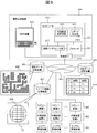
- FIG. 6 is a diagram showing an environment in which the inspection support apparatus 600 of the present embodiment is arranged and the internal configuration of the inspection support apparatus.
- the inspection support apparatus 600 of this embodiment is connected to a design data storage device 605, a wafer information storage device 607, and a defect data storage device 609 via a communication network 604.
- these information storage devices execute various layer manufacturing apparatuses 601 which are semiconductor device manufacturing equipment such as layer 1 manufacturing apparatus, layer 2 manufacturing apparatus... Layer n manufacturing apparatus, and visual inspection of each layer.
- a layer 1 appearance inspection device, a layer 2 appearance inspection device, a layer n appearance inspection device, such as an appearance inspection device 602, and a high-magnification review image of defect candidate positions acquired by the above-described each layer appearance inspection device are executed and ADC is executed.
- a review device 603 such as a layer n review device are connected via a communication network 604.
- the position information of the defect detected by the appearance inspection device 602 is given a defect ID for each newly detected defect and is stored in the defect data storage device 609.
- the wafer ID of the wafer that has been inspected and the process ID that indicates which process in the semiconductor device manufacturing process has been inspected are also stored in the defect data storage device 609.
- the defect review apparatus acquires an image with a resolution sufficient to understand the detailed structure of the defect for each defect ID, and executes ADC based on the acquired image.
- the incidental information of defects obtained as a result of the ADC for example, defect type information, defect size and defect center position data, or magnification information of the image used for executing the ADC is an ID such as a wafer ID or a process ID. At the same time, it is stored in the defect data storage device 609.
- the wafer information storage device 607 includes a die on the wafer, a chip, a design circuit pattern on the chip, position information of each area of the design cell (functional cell), a wafer ID or chip ID that is identification information of the wafer or chip, and manufacturing. Process information, imaging data, and the like are stored.
- the design data storage device 605 includes an identifier indicating a local area of the design layout such as a die ID, a chip ID, and a cell ID, and a layer ID that is identification information of a layer to which the design pattern belongs.
- the process ID that is the manufacturing process information of the design layout data, the mask ID that is the mask information, and the like are stored.
- the inspection support apparatus 600 includes a computer 611 provided with a function for executing various processes necessary for defect determination, and a display for displaying a GUI for inputting setting conditions necessary for defect determination and a determination result.
- the apparatus 612 is comprised.
- the display device also includes input devices such as a keyboard and a mouse for the device user to operate the GUI screen.
- the computer 611 includes a memory 615 that stores software for realizing the main functions of the inspection support apparatus according to the present embodiment, a processor that executes the software stored in the memory, and each piece of information connected to the communication network 604.
- a communication interface unit 617 that executes communication processing with a storage device (server), and a communication terminal 618 to which physical wiring for connecting to the communication network 604 is connected.
- two examples of software that realizes the main functions of the inspection support apparatus according to the present embodiment are defect projection means that executes defect determination and a report creation unit that outputs a defect determination result in a report format. However, this does not indicate that other functions are not implemented.
- FIG. 7 shows functional blocks developed in the memory space of the memory 615 shown in FIG. Further, the functional blocks shown in FIG. 7 are shown as being formed in the memory 615 for convenience, but in reality, the functional blocks shown in FIG. 7 execute the software stored in the memory 615. It is realized by doing. Hereinafter, the operation of the functional block in FIG. 7 will be described in the order in which the criticality determination is performed on given defect information.
- a wafer ID input field and a process ID input field for requesting input of a wafer ID and a process ID of a wafer to be subjected to defect determination are displayed on a GUI screen displayed on the display device 612.
- the defect data reading unit 701 When the user of the apparatus inputs a desired wafer ID and process ID, the defect data reading unit 701 generates a defect data acquisition request using the wafer ID and process ID as a reference key. This acquisition request is shaped into a request packet by the communication interface 617 and transmitted to the defective data storage device 609 via the communication network 604.
- the defect data storage device 609 returns defect data corresponding to the requested wafer ID and process ID in the form of a reply to the request packet.
- the defect data is stored in the defect data storage device 609 including the defect ID, the X coordinate information of the defect corresponding to the defect ID, the Y coordinate information, and the image data of the local area including the defect. For example, it is stored in a format such as a defect table 610 shown in FIG.
- position information of a reference position for origin alignment such as a wafer center position, an orientation flat position, or an appropriate die corner position on the wafer is also included in the form of incidental information.
- the GUI screen on the display device 612 transitions to the origin alignment execution screen.
- the acquired defect position information is displayed in the form of a defect map on a circular diagram showing the entire wafer. Defects on the defect map are displayed in a form that can be visually recognized by the user of the apparatus, such as changing the color classification or the dot shape according to the defect type information found by the ADC.
- the defect position on the defect map displayed on the GUI and the diagram showing the entire wafer are positions expressed in the coordinate system of the inspection support apparatus 600, and the center of the entire wafer is the center of the visual field of the display. Is just displayed.
- position information that can be used for alignment is displayed as a guide on the position information included in the defect data 610, and the apparatus user follows the guide to set a reference point for performing origin alignment as a defect map.
- the center position of the wafer is designated as a reference point for origin alignment.
- the coordinate conversion processing unit 706 calculates a difference between the reference position coordinate expressed in the coordinate system of the inspection support apparatus 600 and the reference position coordinate included in the defect data 610. Execute and calculate the origin alignment amount. As a result, the coordinate origin of the inspection support apparatus 600 and the coordinate origin of the inspection apparatus (for example, a defect review apparatus or an appearance inspection apparatus) that has executed the defect detection are matched.
- the origin alignment executed at this time is an alignment for aligning the coordinate origin of the inspection support apparatus 600 with the coordinate origin of the inspection apparatus that has executed the defect detection, and will be referred to as the first origin alignment below.
- an area designation screen for designating an area for performing defect determination is displayed on the GUI screen on the display device 612.
- the area designation is performed by surrounding a position where defect determination is to be performed with a pointer on the defect map of the entire wafer.
- the reason for specifying the area is that defects that occur in the manufacturing process of semiconductor devices tend to be distributed in specific areas on the wafer according to the type of defect, and the equipment user does not necessarily have defects on the entire wafer surface. This is because the determination is not always desired.
- the wafer chip information reading unit 702 first requests the wafer information storage device 607 for the wafer die ID and position information and the reference position designated at the time of the first origin alignment. .
- This request is also shaped into a request packet by the communication interface 617 and transmitted to the wafer information storage device 607 via the communication network 604.
- the defect data storage device 607 returns the position information of the die corresponding to the requested die ID and the reference position information of the origin alignment in the form of a reply to the request packet.
- the data portion of the returned data packet is extracted by the communication interface 617, returned to the wafer / chip information reading unit 702, and further transferred to the coordinate conversion processing unit 706.
- the coordinate conversion processing unit 706 executes origin alignment with respect to the coordinate system describing the design layout data as described above, and the coordinate origin of the inspection support apparatus 600 and the coordinate origin of the position information stored in the wafer information storage device 607 Align. Hereinafter, this operation is referred to as second origin alignment. After the second origin alignment calculation, the coordinate conversion processing unit 706 converts the acquired die position information into the coordinate system of the inspection support apparatus 600. The converted die position information and die ID are returned to the wafer / chip information reading unit 702.
- the wafer / chip information reading unit 702 executes a process of extracting the die ID of the die included in the designated area using the returned die position information, and all of the extracted ID dies included in each die are executed.
- the wafer information storage device 607 is requested for the chip and cell ID and position information. This request is also transmitted to the wafer information storage device 607 via the communication interface 617, and the wafer information storage device 607 returns the chip ID and chip position information included in the die for the designated ID die.
- the wafer / chip information reading unit 702 transfers the process ID, wafer ID, die ID, and returned chip ID of the wafer whose defect is currently being determined to the design layout data reading unit 703.
- the design layout data reading unit 703 requests the design data storage device 605 to transmit the corresponding design layout data using the acquired process ID, wafer ID, die ID, and chip ID as search keys. This request is also transmitted to the design data storage device 605 via the communication interface 617, and the design data storage device 605 stores the design layout data corresponding to the requested wafer ID, process ID, die ID, chip ID, and cell ID. The data is returned to the design layout data reading unit 703. As described in FIG. 5, there are a plurality of design layout information included in the same process ID. Therefore, the design layout data returned from the design data storage device 605 includes a plurality of layers corresponding to the plurality of design layout information. Design layout data with ID is included. Therefore, the design data storage device 605 also transmits correspondence information indicating which layer ID design layout information has what function (for example, classification of active pattern and dummy pattern). The design layout data reading unit 703 further transfers the returned data to the design cell analysis processing unit 704.
- the design cell analysis processing unit 704 executes a process of assigning an identifier for classifying the active pattern and the dummy pattern with respect to the acquired design layout data using the correspondence information. Thereby, the inspection support apparatus 600 can recognize the classification of the acquired design layout data.
- the assigned identifier information is transmitted to the design layout data drawing processing unit 705, and a design pattern diagram as a background for synthesizing the defect information is generated. This operation is, for example, as shown in FIG.
- FIG. 5 shows that a layer formed by a manufacturing process of a certain process ID is configured by four patterns of a lower layer, a middle layer, an upper layer 2, and an upper layer 1, and different layer IDs according to each pattern, for example, Identifiers such as layer 1, layer 2, layer 3, and layer 4 are assigned in order from the bottom.
- “1” is an identifier meaning a dummy pattern
- 0” is an identifier meaning an active pattern.
- the design layout data drawing processing unit 705 generates a background pattern by discriminating between the active pattern and the dummy pattern based on the design layout data classification code (identifier) given by the design cell analysis processing unit 704. “Generate by discrimination” means, for example, a process of generating an active pattern and a dummy pattern by color-coding, but other expression formats may be used as long as they can be discriminated by the apparatus user.
- a plurality of layer ID patterns included in a certain process ID are designed by the design layout data drawing processing unit 705, which is a design pattern corresponding to the active pattern in FIG. 8A and the design pattern corresponding to the dummy pattern.
- FIG. 8C is a schematic diagram showing a state in which the pattern shown in FIG. 8A and the pattern shown in FIG. 8B are further superimposed.
- the defect image and the defect position information are shown in FIG. Is synthesized on such a background image.
- the generated background pattern is transmitted to the defect-background synthesis processing unit 707.
- the position information of the defect position converted into the coordinate system of the inspection support apparatus 600 is transferred from the coordinate conversion processing unit 706, and the defect image information is transferred from the defect data reading unit 701 to the defect-background synthesis processing unit 707.
- the defect-background synthesis processing unit 707 performs display size adjustment processing for matching the display sizes of the acquired image and the background image from the magnification information included in the acquired image information, and further, the background image, the defect image, and the defect position.
- a process of combining information is executed.
- the combined defect integrated projection image is displayed as a result on the GUI screen, and is used for the apparatus user to visually confirm the criticality of the detected defect.
- the defect ID data to which the identifier for discriminating the active pattern / dummy pattern is assigned is updated in the defect data storage device, and is referred to when ADC is performed on the wafer on which the same kind of circuit pattern is formed. .
- FIG. 9 schematically shows an inspection image (A) before synthesis of the defect integrated projection image, a design wiring pattern (B) as a background, and a defect projection image (C) after the defect-background synthesis processing. . Since it is possible to visually confirm that the defect A existing in the inspection image (A) exists in the dummy pattern area (the pattern hatched in the vertical direction in FIG. (B)) on the defect projection image (C). The device user can determine that the defect A is a non-fatal defect. On the other hand, the defect B present in the inspection image (A) exists in the active pattern region (pattern hatched in FIG. (B)) on the defect projection image (C), and is a fatal defect. It can be determined that there is.
- the user can select a defect from the list and set the defect type and the classification identifier from the design wiring pattern and the inspection image. Specifically, it is easily determined and set whether the defect is on the active pattern or the dummy pattern. This determination process can be automatically calculated by incorporating a calculation process from a wiring pattern and defect coordinates.
- the fatal defect extraction unit 708 shown in FIG. 7 extracts only the corresponding defect according to the condition.
- the extraction result in the fatal defect extraction unit 708 is transferred to the design layout data drawing processing unit 705, and the defect of the coordinate corresponding to the dummy pattern is masked and displayed from the defect integrated projection image displayed on the GUI screen.
- the defect of coordinates corresponding to the dummy pattern may not be displayed.
- FIG. 10 shows an example of a screening result displayed on the screen after execution of the critical defect screening process before and after the execution.
- FIGS. 10A and 10B show the defect map format showing the entire wafer
- FIGS. 10C and 10D show the screening results in a format in which a part of the cell is enlarged.
- FIG. 10B it can be seen that the distribution area of the fatal defects can be specified more than in FIG. 10A because the non-fatal defects are removed and displayed.
- the design layout data to be combined with the inspection image in the defect integrated projection processing is not necessarily limited to the data on the same layer, and data on different layers can be combined.
- FIG. 11 shows a state in which a design pattern of a downstream process, that is, a design pattern of a hierarchy to be formed on the layer from which the inspection image is acquired is synthesized. Since the origin alignment process and coordinate conversion process at the time of composition are the same as those at the time of synthesizing layout data of the same layer, the description will not be repeated.
- FIG. 11A shows an inspection image
- FIG. 11B shows design layout data in the downstream process (assuming all are active patterns for simplicity)
- FIG. 11C shows a defect integrated projection image after synthesis.
- the two defects A and B shown in FIG. 11A are both defects existing between the wirings, and both are recognized as non-fatal defects on the inspection image.
- defect A is present at a location where no pattern is present on the design pattern of the downstream process
- defect B is present at a location where the pattern is present. Therefore, defect A affects the downstream process.
- the defect integrated projection image with the design layout data of different layers as shown in FIG. 11C displays a button such as “Difference with different layers” on the GUI, so that the user of the device has the different layers.
- the synthesis process is started by inputting whether or not the defect integrated projection image needs to be acquired and the ID of the hierarchy (eg, process ID and layer ID) to be viewed.
- the process executed at this time is that the design layout data reading unit 703 acquires the design layout data using the process ID input on the GUI instead of the process ID acquired by the defect data reading unit 701. Since the processing already described is the same, the description is omitted. It goes without saying that active / dummy pattern discrimination display is also possible for design layout data at different levels.
Landscapes
- Engineering & Computer Science (AREA)
- Physics & Mathematics (AREA)
- General Physics & Mathematics (AREA)
- Theoretical Computer Science (AREA)
- Quality & Reliability (AREA)
- Computer Vision & Pattern Recognition (AREA)
- Health & Medical Sciences (AREA)
- Life Sciences & Earth Sciences (AREA)
- Chemical & Material Sciences (AREA)
- Analytical Chemistry (AREA)
- Biochemistry (AREA)
- General Health & Medical Sciences (AREA)
- Immunology (AREA)
- Pathology (AREA)
- Testing Or Measuring Of Semiconductors Or The Like (AREA)
Abstract
Description
<半導体欠陥統合投影システムの構成>
図1は、本発明の実施形態を示す半導体欠陥統合投影システムの説明である。
設計レイアウトデータに欠陥表示を投影する欠陥統合投影表示の例を図2に示す。ここでは、ウェーハ、ダイ、チップ、セルの順に、大きい単位から小さい単位へ、欠陥情報と設計レイアウトデータとを統合投影表示させる。
201は、検査ウェーハ上に複数ならんだダイの欠陥情報(黒丸)と設計レイアウトデータとを統合投影表示した図である。
ダイ上に複数の半導体チップが形成され、複数のチップ全体で一つの半導体デバイスとして動作する場合もある。203は、ダイ上に複数並んだチップの欠陥情報(黒丸)と設計レイアウトデータとを統合投影表示した図である。
205は、チップ上に複数ならんだセルの欠陥情報(黒丸)と設計レイアウトデータとを統合投影表示した図である。
設計レイアウトデータ欠陥統合投影の拡大表示例を図3に示す。ここでは、チップ全体からでは欠陥の状態が判らない問題を考慮し、欠陥部分を自動または手動で拡大表示することを可能とした。また、1つのチップを製造するためのそれぞれの工程に対応するそれぞれの設計レイアウトデータのうち、検査時の工程に応じた設計レイアウトデータ上に対して欠陥位置を画面に表示させることを可能とした。
欠陥統合投影手段2により統合投影する処理のフローチャートを図4に示す。
S407の場合、欠陥座標のダイ座標への座標変換が実行されるので、座標変換処理部25は、まず、原点アライメントを実行し、レイアウトパターンの座標系と検査装置の座標系の原点を一致させる。次に、画面表示するダイのダイIDから原点オフセット量を認識し、欠陥位置の座標情報に加算することにより、ダイ座標への座標変換を実行する。なお、欠陥データの座標が検査装置の持つダイ座標で記憶されている場合は、検査装置のダイ座標を表現する座標系とレイアウトパターン上でのダイの座標系との原点アライメントのみを実行し、ウェーハ全体の座標系からダイの座標系への原点オフセット調整は行わない。
なお、本発明は、実施形態の機能を実現するソフトウェアのプログラムコードによっても実現できる。この場合、プログラムコードを記録した記憶媒体をシステム或は装置に提供し、そのシステム或は装置のコンピュータ(又はCPUやMPU)が記憶媒体に格納されたプログラムコードを読み出す。この場合、記憶媒体から読み出されたプログラムコード自体が前述した実施形態の機能を実現することになり、そのプログラムコード自体、及びそれを記憶した記憶媒体は本発明を構成することになる。このようなプログラムコードを供給するための記憶媒体としては、例えば、フロッピィ(登録商標)ディスク、CD-ROM、DVD-ROM、ハードディスク、光ディスク、光磁気ディスク、CD-R、磁気テープ、不揮発性のメモリカード、ROMなどが用いられる。
[背景技術]で説明した通り、半導体デバイスの製造プロセスにおいては、近年、設計起因による欠陥が増加しつつあり、設計起因による欠陥の原因を早急に突き止め、設計へ反映し、歩留まりを向上させることが課題となっている。このため、従来から、特許文献1~3に開示されているように設計レイアウトの参照機能を組み込んだ検査装置が使用されている。
2 欠陥統合投影手段
3 欠陥統合投影表示装置
4 欠陥統合投影指示情報入力装置
5 設計レイアウトデータ記憶装置
6 ウェーハデータ記憶装置
7 欠陥データ記憶装置
Claims (9)
- 半導体製造の各工程で用いられる設計回路パターンの位置情報を含む設計レイアウトデータを取得する設計レイアウトデータ読込み部と、
前記設計回路パターンがチップ毎に複数形成されたウェーハに関するデータの中から少なくとも設計セルの位置情報を含むウェーハ・チップ情報を取得するウェーハ・チップ情報読込み部と、
前記各工程で生じた欠陥の位置情報を含む欠陥データを取得する欠陥データ読込み部と、
前記設計レイアウトデータと前記ウェーハ・チップ情報に基づき、前記設計レイアウトデータのうち欠陥が生じた工程における設計レイアウトデータと前記欠陥データとを統合投影処理することで、設計レイアウトデータ欠陥統合投影表示図を作成する設計レイアウトデータ描画処理部と、
前記設計レイアウトデータ欠陥統合投影表示図を表示する欠陥統合投影表示装置と、を備えることを特徴とする半導体欠陥検査支援装置。 - 半導体デバイスを構成する複数の階層の回路パターンに対する欠陥位置の検査結果と、前記複数の階層の回路パターンに対する設計レイアウト情報とがそれぞれ格納された複数の情報記憶装置に接続されて使用され、前記検査結果と設計レイアウト情報とを画面表示することにより、前記欠陥検査の支援作業を実行する欠陥検査支援装置において、
所定の基準位置の座標情報を用いて、前記欠陥位置の座標を記述する座標系の座標原点と自身の持つ座標系の座標原点とを整合させる第1の原点アライメントおよび前記設計レイアウト情報を記述する座標系の座標原点と自身の持つ座標系の座標原点とを整合させる第2の原点アライメントを実行する手段と、
前記設計レイアウト情報から得られる回路パターンと前記欠陥とを合成して欠陥統合投影画像を生成する手段と、
前記欠陥統合投影画像を表示する画面表示手段とを備えることを特徴とする欠陥検査支援装置。 - 請求項2に記載の欠陥検査支援装置において、
前記画面表示手段には、前記欠陥統合投影画像の背景となる前記回路パターンが属するの階層を特定するための識別情報を入力させるための入力欄が表示され、
前記欠陥検査支援装置は、更に、
前記入力された識別情報に対応する階層の設計レイアウト情報を前記情報記憶装置に対して要求し、該設計レイアウト情報を取得する設計レイアウトデータ読み込み部を備えたことを特徴とする欠陥検査支援装置。 - 請求項2に記載の欠陥検査支援装置において、
欠陥統合投影画像として、少なくとも半導体ウェーハ全体と当該半導体ウェーハの局所領域の少なくとも2つを生成可能なことを特徴とする欠陥検査支援装置。 - 請求項4に記載の欠陥検査支援装置において、
前記局所領域の設計レイアウト情報は、当該局所領域のサイズに応じた固有の座標系を有しており、
前記欠陥位置の座標を、前記局所領域のサイズ単位に応じた固有の座標系に変換する座標変換を行う手段を備えたことを特徴とする欠陥検査支援装置。 - 請求項5に記載の欠陥検査支援装置において、
前記局所領域のサイズ単位が、ダイ単位、チップ単位、セル単位を含むことを特徴とする欠陥検査支援装置。 - 請求項2に記載の欠陥検査支援装置において、
前記回路パターンを、当該パターンに含まれるアクティブパターンとダミーパターンとに弁別して前記欠陥統合投影画像の背景画像を生成することを特徴とする欠陥検査支援装置。 - 請求項7に記載の欠陥検査支援装置において、
前記ダミーパターンに重なって表示される欠陥が前記画面表示手段上にマスクして表示されることを特徴とする欠陥検査支援装置。 - 請求項7に記載の欠陥検査支援装置において、
前記アクティブパターン上に存在する欠陥のみをスクリーニングして表示する機能を備えたことを特徴とする欠陥検査支援装置。
Priority Applications (3)
| Application Number | Priority Date | Filing Date | Title |
|---|---|---|---|
| JP2010549455A JP5395814B2 (ja) | 2009-02-04 | 2010-02-01 | 半導体欠陥統合投影方法および半導体欠陥統合投影機能を実装した欠陥検査支援装置 |
| KR1020117018136A KR101324349B1 (ko) | 2009-02-04 | 2010-02-01 | 반도체 결함 통합 투영 방법 및 반도체 결함 통합 투영 기능을 실장한 결함 검사 지원 장치 |
| US13/147,899 US20110296362A1 (en) | 2009-02-04 | 2010-02-01 | Semiconductor defect integrated projection method and defect inspection support apparatus equipped with semiconductor defect integrated projection function |
Applications Claiming Priority (2)
| Application Number | Priority Date | Filing Date | Title |
|---|---|---|---|
| JP2009023178 | 2009-02-04 | ||
| JP2009-023178 | 2009-02-04 |
Publications (1)
| Publication Number | Publication Date |
|---|---|
| WO2010090152A1 true WO2010090152A1 (ja) | 2010-08-12 |
Family
ID=42542046
Family Applications (1)
| Application Number | Title | Priority Date | Filing Date |
|---|---|---|---|
| PCT/JP2010/051319 Ceased WO2010090152A1 (ja) | 2009-02-04 | 2010-02-01 | 半導体欠陥統合投影方法および半導体欠陥統合投影機能を実装した欠陥検査支援装置 |
Country Status (4)
| Country | Link |
|---|---|
| US (1) | US20110296362A1 (ja) |
| JP (1) | JP5395814B2 (ja) |
| KR (1) | KR101324349B1 (ja) |
| WO (1) | WO2010090152A1 (ja) |
Cited By (9)
| Publication number | Priority date | Publication date | Assignee | Title |
|---|---|---|---|---|
| WO2012077497A1 (ja) * | 2010-12-06 | 2012-06-14 | 株式会社日立ハイテクノロジーズ | 欠陥検査装置 |
| KR101800493B1 (ko) | 2011-04-26 | 2017-11-22 | 케이엘에이-텐코 코포레이션 | 데이터베이스 기반 셀-대-셀 레티클 검사 |
| JP2019509628A (ja) * | 2016-02-04 | 2019-04-04 | ケーエルエー−テンカー コーポレイション | デザインファイルまたは検査画像を用いた自動デスキュー |
| JP2019132594A (ja) * | 2018-01-29 | 2019-08-08 | セイコーエプソン株式会社 | 検査装置及び検査方法 |
| JP2019527475A (ja) * | 2016-06-29 | 2019-09-26 | ケーエルエー コーポレイション | 感度改善およびニューサンス抑制のため、論理的およびホットスポット検査でzレイヤコンテキストを使用するシステムおよび方法 |
| CN111340788A (zh) * | 2020-02-28 | 2020-06-26 | 中国电子产品可靠性与环境试验研究所((工业和信息化部电子第五研究所)(中国赛宝实验室)) | 硬件木马版图检测方法、装置、电子设备和可读存储介质 |
| JP2021022257A (ja) * | 2019-07-30 | 2021-02-18 | 三菱パワー株式会社 | 点検支援システム、サーバ装置、点検支援方法、及び点検支援プログラム |
| JPWO2021192272A1 (ja) * | 2020-03-27 | 2021-09-30 | ||
| CN117034853A (zh) * | 2022-11-25 | 2023-11-10 | 上海华大九天信息科技有限公司 | 检查ro版图正确性的方法、装置及相关产品 |
Families Citing this family (21)
| Publication number | Priority date | Publication date | Assignee | Title |
|---|---|---|---|---|
| US9129237B2 (en) * | 2011-12-28 | 2015-09-08 | Elitetech Technology Co., Ltd. | Integrated interfacing system and method for intelligent defect yield solutions |
| US9269135B2 (en) * | 2012-03-01 | 2016-02-23 | Taiwan Semiconductor Manufacturing Company, Ltd. | Defect management systems and methods |
| US9858658B2 (en) * | 2012-04-19 | 2018-01-02 | Applied Materials Israel Ltd | Defect classification using CAD-based context attributes |
| US9595091B2 (en) | 2012-04-19 | 2017-03-14 | Applied Materials Israel, Ltd. | Defect classification using topographical attributes |
| US10192303B2 (en) | 2012-11-12 | 2019-01-29 | Kla Tencor Corporation | Method and system for mixed mode wafer inspection |
| US9347862B2 (en) * | 2013-08-06 | 2016-05-24 | Kla-Tencor Corp. | Setting up a wafer inspection process using programmed defects |
| US10410338B2 (en) | 2013-11-04 | 2019-09-10 | Kla-Tencor Corporation | Method and system for correlating optical images with scanning electron microscopy images |
| US10712289B2 (en) * | 2014-07-29 | 2020-07-14 | Kla-Tencor Corp. | Inspection for multiple process steps in a single inspection process |
| WO2016092640A1 (ja) * | 2014-12-10 | 2016-06-16 | 株式会社 日立ハイテクノロジーズ | 欠陥観察装置および欠陥観察方法 |
| US10650509B2 (en) | 2016-09-08 | 2020-05-12 | Synopsys, Inc. | Video overlay |
| US10102615B2 (en) * | 2016-12-14 | 2018-10-16 | Taiwan Semiconductor Manufacturing Co., Ltd. | Method and system for detecting hotspots in semiconductor wafer |
| EP3454128B1 (en) * | 2017-09-12 | 2020-01-29 | IMEC vzw | A method and system for detecting defects of a lithographic pattern |
| CN110727247B (zh) * | 2018-07-17 | 2022-10-04 | 敖翔科技股份有限公司 | 半导体厂缺陷操作系统及装置 |
| US20200134829A1 (en) | 2018-10-30 | 2020-04-30 | Fei Company | Artificial Intelligence Enabled Metrology |
| CN111368492B (zh) * | 2018-12-24 | 2023-09-01 | 上海新微技术研发中心有限公司 | 一种用于在集成电路版图中设置标识信息的方法及系统 |
| US10801953B2 (en) * | 2019-01-11 | 2020-10-13 | Kla-Tencor Corporation | Semiconductor metrology based on hyperspectral imaging |
| CN115176281B (zh) * | 2020-03-03 | 2026-02-27 | 富士胶片株式会社 | 三维显示装置、方法及计算机可读取记录介质 |
| CN114240817B (zh) * | 2020-09-09 | 2025-01-17 | 长鑫存储技术有限公司 | 数据分析方法及装置、电子设备、存储介质 |
| WO2022180827A1 (ja) * | 2021-02-26 | 2022-09-01 | 日本電信電話株式会社 | 光学特性のai予測システム |
| CN116539639A (zh) * | 2023-04-26 | 2023-08-04 | 深圳和美精艺半导体科技股份有限公司 | Aoi检测方法、装置、电子设备和存储介质 |
| KR102639655B1 (ko) * | 2023-07-11 | 2024-02-23 | 주식회사 에이아이비즈 | 웨이퍼맵의 패턴을 분류하기 위한 방법, 장치 및 프로그램 |
Citations (4)
| Publication number | Priority date | Publication date | Assignee | Title |
|---|---|---|---|---|
| JPH09266235A (ja) * | 1996-03-28 | 1997-10-07 | Sony Corp | 不良解析方法とそのシステム |
| JPH11251377A (ja) * | 1998-03-02 | 1999-09-17 | Hitachi Ltd | 欠陥検査方法およびその装置並びに欠陥の観察または分析方法およびそのシステム |
| JP2003023056A (ja) * | 2001-07-10 | 2003-01-24 | Hitachi Ltd | 半導体デバイスの欠陥分類方法および半導体デバイスの歩留まり予測方法および半導体デバイスの製造方法および半導体デバイスの欠陥分類システムおよび半導体デバイス分類装置およびそれらに用いるプログラムおよび記録媒体 |
| JP2003100825A (ja) * | 2001-09-20 | 2003-04-04 | Hitachi Ltd | 半導体装置の製造方法並びに欠陥検査データ処理方法及びその装置 |
Family Cites Families (10)
| Publication number | Priority date | Publication date | Assignee | Title |
|---|---|---|---|---|
| JP3484042B2 (ja) * | 1997-05-21 | 2004-01-06 | 株式会社日立製作所 | パターン検査方法およびその装置 |
| US6107637A (en) * | 1997-08-11 | 2000-08-22 | Hitachi, Ltd. | Electron beam exposure or system inspection or measurement apparatus and its method and height detection apparatus |
| KR100610175B1 (ko) * | 1999-03-24 | 2006-08-09 | 후지쯔 가부시끼가이샤 | 반도체 장치의 제조 방법 및 칩 식별 정보의 기록 방법 |
| US6900888B2 (en) * | 2001-09-13 | 2005-05-31 | Hitachi High-Technologies Corporation | Method and apparatus for inspecting a pattern formed on a substrate |
| US9002497B2 (en) | 2003-07-03 | 2015-04-07 | Kla-Tencor Technologies Corp. | Methods and systems for inspection of wafers and reticles using designer intent data |
| KR20070036217A (ko) * | 2005-09-29 | 2007-04-03 | 주식회사 하이닉스반도체 | 레티클의 결함 검사 방법 |
| US7570796B2 (en) * | 2005-11-18 | 2009-08-04 | Kla-Tencor Technologies Corp. | Methods and systems for utilizing design data in combination with inspection data |
| US7676077B2 (en) * | 2005-11-18 | 2010-03-09 | Kla-Tencor Technologies Corp. | Methods and systems for utilizing design data in combination with inspection data |
| US8041103B2 (en) * | 2005-11-18 | 2011-10-18 | Kla-Tencor Technologies Corp. | Methods and systems for determining a position of inspection data in design data space |
| JP2009260176A (ja) * | 2008-04-21 | 2009-11-05 | Nec Electronics Corp | 半導体装置の信頼性予測方法、及びそのプログラム |
-
2010
- 2010-02-01 US US13/147,899 patent/US20110296362A1/en not_active Abandoned
- 2010-02-01 JP JP2010549455A patent/JP5395814B2/ja active Active
- 2010-02-01 WO PCT/JP2010/051319 patent/WO2010090152A1/ja not_active Ceased
- 2010-02-01 KR KR1020117018136A patent/KR101324349B1/ko active Active
Patent Citations (4)
| Publication number | Priority date | Publication date | Assignee | Title |
|---|---|---|---|---|
| JPH09266235A (ja) * | 1996-03-28 | 1997-10-07 | Sony Corp | 不良解析方法とそのシステム |
| JPH11251377A (ja) * | 1998-03-02 | 1999-09-17 | Hitachi Ltd | 欠陥検査方法およびその装置並びに欠陥の観察または分析方法およびそのシステム |
| JP2003023056A (ja) * | 2001-07-10 | 2003-01-24 | Hitachi Ltd | 半導体デバイスの欠陥分類方法および半導体デバイスの歩留まり予測方法および半導体デバイスの製造方法および半導体デバイスの欠陥分類システムおよび半導体デバイス分類装置およびそれらに用いるプログラムおよび記録媒体 |
| JP2003100825A (ja) * | 2001-09-20 | 2003-04-04 | Hitachi Ltd | 半導体装置の製造方法並びに欠陥検査データ処理方法及びその装置 |
Cited By (17)
| Publication number | Priority date | Publication date | Assignee | Title |
|---|---|---|---|---|
| WO2012077497A1 (ja) * | 2010-12-06 | 2012-06-14 | 株式会社日立ハイテクノロジーズ | 欠陥検査装置 |
| JP2012122765A (ja) * | 2010-12-06 | 2012-06-28 | Hitachi High-Technologies Corp | 欠陥検査装置 |
| TWI464394B (zh) * | 2010-12-06 | 2014-12-11 | Hitachi High Tech Corp | Defect detection device |
| KR101800493B1 (ko) | 2011-04-26 | 2017-11-22 | 케이엘에이-텐코 코포레이션 | 데이터베이스 기반 셀-대-셀 레티클 검사 |
| JP2019509628A (ja) * | 2016-02-04 | 2019-04-04 | ケーエルエー−テンカー コーポレイション | デザインファイルまたは検査画像を用いた自動デスキュー |
| JP2019527475A (ja) * | 2016-06-29 | 2019-09-26 | ケーエルエー コーポレイション | 感度改善およびニューサンス抑制のため、論理的およびホットスポット検査でzレイヤコンテキストを使用するシステムおよび方法 |
| JP2019132594A (ja) * | 2018-01-29 | 2019-08-08 | セイコーエプソン株式会社 | 検査装置及び検査方法 |
| JP7052377B2 (ja) | 2018-01-29 | 2022-04-12 | セイコーエプソン株式会社 | 検査装置及び検査方法 |
| JP2021022257A (ja) * | 2019-07-30 | 2021-02-18 | 三菱パワー株式会社 | 点検支援システム、サーバ装置、点検支援方法、及び点検支援プログラム |
| JP7339051B2 (ja) | 2019-07-30 | 2023-09-05 | 三菱重工業株式会社 | 点検支援システム、サーバ装置、点検支援方法、及び点検支援プログラム |
| CN111340788A (zh) * | 2020-02-28 | 2020-06-26 | 中国电子产品可靠性与环境试验研究所((工业和信息化部电子第五研究所)(中国赛宝实验室)) | 硬件木马版图检测方法、装置、电子设备和可读存储介质 |
| CN111340788B (zh) * | 2020-02-28 | 2024-03-29 | 中国电子产品可靠性与环境试验研究所((工业和信息化部电子第五研究所)(中国赛宝实验室)) | 硬件木马版图检测方法、装置、电子设备和可读存储介质 |
| JPWO2021192272A1 (ja) * | 2020-03-27 | 2021-09-30 | ||
| WO2021192272A1 (ja) * | 2020-03-27 | 2021-09-30 | 株式会社図研 | 設計支援装置、設計支援方法およびプログラム |
| JP7464696B2 (ja) | 2020-03-27 | 2024-04-09 | 株式会社図研 | 設計支援装置、設計支援方法およびプログラム |
| US12572710B2 (en) | 2020-03-27 | 2026-03-10 | Kabushiki Kaisha Zuken | Support apparatus, design support method, and non-transitory computer readable medium storing a computer program |
| CN117034853A (zh) * | 2022-11-25 | 2023-11-10 | 上海华大九天信息科技有限公司 | 检查ro版图正确性的方法、装置及相关产品 |
Also Published As
| Publication number | Publication date |
|---|---|
| US20110296362A1 (en) | 2011-12-01 |
| KR20110105852A (ko) | 2011-09-27 |
| JPWO2010090152A1 (ja) | 2012-08-09 |
| KR101324349B1 (ko) | 2013-10-31 |
| JP5395814B2 (ja) | 2014-01-22 |
Similar Documents
| Publication | Publication Date | Title |
|---|---|---|
| JP5395814B2 (ja) | 半導体欠陥統合投影方法および半導体欠陥統合投影機能を実装した欠陥検査支援装置 | |
| JP5021503B2 (ja) | パターン欠陥解析装置、パターン欠陥解析方法およびパターン欠陥解析プログラム | |
| US8068662B2 (en) | Method and system for determining a defect during charged particle beam inspection of a sample | |
| TWI512684B (zh) | Defect observation method and defect observation device | |
| US20210231582A1 (en) | Smart coordinate conversion and calibration system in semiconductor wafer manufacturing | |
| CN100562878C (zh) | 缺陷检查系统及缺陷检查方法 | |
| US8547429B2 (en) | Apparatus and method for monitoring semiconductor device manufacturing process | |
| JP5479782B2 (ja) | 欠陥画像処理装置、欠陥画像処理方法、半導体欠陥分類装置および半導体欠陥分類方法 | |
| JP6080379B2 (ja) | 半導体欠陥分類装置及び半導体欠陥分類装置用のプログラム | |
| US9040937B2 (en) | Charged particle beam apparatus | |
| JP2011222622A (ja) | 検査方法およびその装置 | |
| JP2009250645A (ja) | 欠陥レビュー方法およびその装置 | |
| JP2010165876A (ja) | 欠陥関連付け装置、基板検査システム、および欠陥関連付け方法 | |
| US8472696B2 (en) | Observation condition determination support device and observation condition determination support method | |
| JP5470008B2 (ja) | 設計データを利用した欠陥レビュー装置および欠陥検査システム | |
| US20130283227A1 (en) | Pattern review tool, recipe making tool, and method of making recipe | |
| JP5469704B2 (ja) | 欠陥解析装置、欠陥解析方法および欠陥解析プログラム | |
| JP5039594B2 (ja) | レビュー装置,検査領域設定支援システム、および、欠陥の画像得方法 | |
| WO2018167965A1 (ja) | 欠陥観察装置及び欠陥観察方法 | |
| JP2021162527A (ja) | 半導体の欠陥検出装置及びプログラム | |
| JP2008014717A (ja) | 欠陥検査システムおよび欠陥検査方法 | |
| JP4199759B2 (ja) | インデックス情報作成装置、試料検査装置、レビュー装置、インデックス情報作成方法及びプログラム | |
| JP6138460B2 (ja) | 荷電粒子線装置 |
Legal Events
| Date | Code | Title | Description |
|---|---|---|---|
| 121 | Ep: the epo has been informed by wipo that ep was designated in this application |
Ref document number: 10738484 Country of ref document: EP Kind code of ref document: A1 |
|
| ENP | Entry into the national phase |
Ref document number: 2010549455 Country of ref document: JP Kind code of ref document: A |
|
| ENP | Entry into the national phase |
Ref document number: 20117018136 Country of ref document: KR Kind code of ref document: A |
|
| NENP | Non-entry into the national phase |
Ref country code: DE |
|
| WWE | Wipo information: entry into national phase |
Ref document number: 13147899 Country of ref document: US |
|
| 122 | Ep: pct application non-entry in european phase |
Ref document number: 10738484 Country of ref document: EP Kind code of ref document: A1 |