WO2010038445A1 - フォトマスクブランク、フォトマスク及びその製造方法、並びに半導体デバイスの製造方法 - Google Patents
フォトマスクブランク、フォトマスク及びその製造方法、並びに半導体デバイスの製造方法 Download PDFInfo
- Publication number
- WO2010038445A1 WO2010038445A1 PCT/JP2009/005021 JP2009005021W WO2010038445A1 WO 2010038445 A1 WO2010038445 A1 WO 2010038445A1 JP 2009005021 W JP2009005021 W JP 2009005021W WO 2010038445 A1 WO2010038445 A1 WO 2010038445A1
- Authority
- WO
- WIPO (PCT)
- Prior art keywords
- film
- light
- etching mask
- light shielding
- photomask
- Prior art date
- Legal status (The legal status is an assumption and is not a legal conclusion. Google has not performed a legal analysis and makes no representation as to the accuracy of the status listed.)
- Ceased
Links
Images







Classifications
-
- G—PHYSICS
- G03—PHOTOGRAPHY; CINEMATOGRAPHY; ANALOGOUS TECHNIQUES USING WAVES OTHER THAN OPTICAL WAVES; ELECTROGRAPHY; HOLOGRAPHY
- G03F—PHOTOMECHANICAL PRODUCTION OF TEXTURED OR PATTERNED SURFACES, e.g. FOR PRINTING, FOR PROCESSING OF SEMICONDUCTOR DEVICES; MATERIALS THEREFOR; ORIGINALS THEREFOR; APPARATUS SPECIALLY ADAPTED THEREFOR
- G03F1/00—Originals for photomechanical production of textured or patterned surfaces, e.g., masks, photo-masks, reticles; Mask blanks or pellicles therefor; Containers specially adapted therefor; Preparation thereof
- G03F1/50—Mask blanks not covered by G03F1/20 - G03F1/34; Preparation thereof
-
- G—PHYSICS
- G03—PHOTOGRAPHY; CINEMATOGRAPHY; ANALOGOUS TECHNIQUES USING WAVES OTHER THAN OPTICAL WAVES; ELECTROGRAPHY; HOLOGRAPHY
- G03F—PHOTOMECHANICAL PRODUCTION OF TEXTURED OR PATTERNED SURFACES, e.g. FOR PRINTING, FOR PROCESSING OF SEMICONDUCTOR DEVICES; MATERIALS THEREFOR; ORIGINALS THEREFOR; APPARATUS SPECIALLY ADAPTED THEREFOR
- G03F1/00—Originals for photomechanical production of textured or patterned surfaces, e.g., masks, photo-masks, reticles; Mask blanks or pellicles therefor; Containers specially adapted therefor; Preparation thereof
- G03F1/22—Masks or mask blanks for imaging by radiation of 100nm or shorter wavelength, e.g. X-ray masks, extreme ultraviolet [EUV] masks; Preparation thereof
-
- G—PHYSICS
- G03—PHOTOGRAPHY; CINEMATOGRAPHY; ANALOGOUS TECHNIQUES USING WAVES OTHER THAN OPTICAL WAVES; ELECTROGRAPHY; HOLOGRAPHY
- G03F—PHOTOMECHANICAL PRODUCTION OF TEXTURED OR PATTERNED SURFACES, e.g. FOR PRINTING, FOR PROCESSING OF SEMICONDUCTOR DEVICES; MATERIALS THEREFOR; ORIGINALS THEREFOR; APPARATUS SPECIALLY ADAPTED THEREFOR
- G03F1/00—Originals for photomechanical production of textured or patterned surfaces, e.g., masks, photo-masks, reticles; Mask blanks or pellicles therefor; Containers specially adapted therefor; Preparation thereof
- G03F1/54—Absorbers, e.g. of opaque materials
-
- G—PHYSICS
- G03—PHOTOGRAPHY; CINEMATOGRAPHY; ANALOGOUS TECHNIQUES USING WAVES OTHER THAN OPTICAL WAVES; ELECTROGRAPHY; HOLOGRAPHY
- G03F—PHOTOMECHANICAL PRODUCTION OF TEXTURED OR PATTERNED SURFACES, e.g. FOR PRINTING, FOR PROCESSING OF SEMICONDUCTOR DEVICES; MATERIALS THEREFOR; ORIGINALS THEREFOR; APPARATUS SPECIALLY ADAPTED THEREFOR
- G03F1/00—Originals for photomechanical production of textured or patterned surfaces, e.g., masks, photo-masks, reticles; Mask blanks or pellicles therefor; Containers specially adapted therefor; Preparation thereof
- G03F1/62—Pellicles, e.g. pellicle assemblies, e.g. having membrane on support frame; Preparation thereof
-
- G—PHYSICS
- G03—PHOTOGRAPHY; CINEMATOGRAPHY; ANALOGOUS TECHNIQUES USING WAVES OTHER THAN OPTICAL WAVES; ELECTROGRAPHY; HOLOGRAPHY
- G03F—PHOTOMECHANICAL PRODUCTION OF TEXTURED OR PATTERNED SURFACES, e.g. FOR PRINTING, FOR PROCESSING OF SEMICONDUCTOR DEVICES; MATERIALS THEREFOR; ORIGINALS THEREFOR; APPARATUS SPECIALLY ADAPTED THEREFOR
- G03F1/00—Originals for photomechanical production of textured or patterned surfaces, e.g., masks, photo-masks, reticles; Mask blanks or pellicles therefor; Containers specially adapted therefor; Preparation thereof
- G03F1/68—Preparation processes not covered by groups G03F1/20 - G03F1/50
-
- G—PHYSICS
- G03—PHOTOGRAPHY; CINEMATOGRAPHY; ANALOGOUS TECHNIQUES USING WAVES OTHER THAN OPTICAL WAVES; ELECTROGRAPHY; HOLOGRAPHY
- G03F—PHOTOMECHANICAL PRODUCTION OF TEXTURED OR PATTERNED SURFACES, e.g. FOR PRINTING, FOR PROCESSING OF SEMICONDUCTOR DEVICES; MATERIALS THEREFOR; ORIGINALS THEREFOR; APPARATUS SPECIALLY ADAPTED THEREFOR
- G03F1/00—Originals for photomechanical production of textured or patterned surfaces, e.g., masks, photo-masks, reticles; Mask blanks or pellicles therefor; Containers specially adapted therefor; Preparation thereof
- G03F1/68—Preparation processes not covered by groups G03F1/20 - G03F1/50
- G03F1/80—Etching
-
- H—ELECTRICITY
- H10—SEMICONDUCTOR DEVICES; ELECTRIC SOLID-STATE DEVICES NOT OTHERWISE PROVIDED FOR
- H10P—GENERIC PROCESSES OR APPARATUS FOR THE MANUFACTURE OR TREATMENT OF DEVICES COVERED BY CLASS H10
- H10P76/00—Manufacture or treatment of masks on semiconductor bodies, e.g. by lithography or photolithography
- H10P76/20—Manufacture or treatment of masks on semiconductor bodies, e.g. by lithography or photolithography of masks comprising organic materials
- H10P76/204—Manufacture or treatment of masks on semiconductor bodies, e.g. by lithography or photolithography of masks comprising organic materials of organic photoresist masks
- H10P76/2041—Photolithographic processes
-
- H—ELECTRICITY
- H10—SEMICONDUCTOR DEVICES; ELECTRIC SOLID-STATE DEVICES NOT OTHERWISE PROVIDED FOR
- H10P—GENERIC PROCESSES OR APPARATUS FOR THE MANUFACTURE OR TREATMENT OF DEVICES COVERED BY CLASS H10
- H10P76/00—Manufacture or treatment of masks on semiconductor bodies, e.g. by lithography or photolithography
- H10P76/40—Manufacture or treatment of masks on semiconductor bodies, e.g. by lithography or photolithography of masks comprising inorganic materials
- H10P76/408—Manufacture or treatment of masks on semiconductor bodies, e.g. by lithography or photolithography of masks comprising inorganic materials characterised by their sizes, orientations, dispositions, behaviours or shapes
- H10P76/4085—Manufacture or treatment of masks on semiconductor bodies, e.g. by lithography or photolithography of masks comprising inorganic materials characterised by their sizes, orientations, dispositions, behaviours or shapes characterised by the processes involved to create the masks
Definitions
- the present invention relates to a photomask blank, a photomask, a manufacturing method thereof, and the like used in manufacturing a semiconductor device or the like.
- Miniaturization of semiconductor devices and the like has an advantage of improving performance and functions (high-speed operation, low power consumption, etc.) and cost reduction, and miniaturization is increasingly accelerated.
- Lithography technology supports this miniaturization, and a transfer mask is a key technology along with an exposure apparatus and a resist material.
- hp half-pitch
- This method uses, for example, a blank in which a MoSi-based light-shielding film / Cr-based etching mask film (also serving as an antireflection film) is formed on a substrate (see the column [0174], etc.).
- a thin Cr-based etching mask film By using a thin Cr-based etching mask film, the burden on the resist is reduced, and the reduction in resolution when a mask pattern is transferred to a thin Cr-based etching mask film is improved. Is done.
- the etching mask film having a higher etching selectivity with respect to the light shielding film than the resist and having a significantly thin film thickness as compared with the resist serves as an etching mask for the light shielding film. It is intended to improve.
- Patent Document 2 describes, for example, a light shielding film having a laminated structure of MoSiN main light shielding layer / MoSiON antireflection layer from the substrate side as a light shielding film having a laminated structure of MoSi-based materials.
- the thickness of the resist film is reduced from the viewpoint of reducing the aspect ratio of the resist pattern and preventing the resist pattern from collapsing. Needs to be 100 nm or less. In order to make the film thickness of the resist film 100 nm or less, the present inventor has found that the layer structure of the conventional photomask blank described above is insufficient, and it is necessary to improve both the etching mask and the light shielding film. It was.
- the etching mask film it is necessary to improve the structure of the etching mask film so that the mask pattern can be transferred to the etching mask with a resist film thickness of 100 nm or less, but it is not sufficient to simply reduce the thickness of the etching mask film. Since the etching mask film must be able to maintain the mask pattern until the etching process for transferring the mask pattern to the lower light shielding film is completed, the conventional etching mask film configuration and the conventional light shielding film configuration can be realized. The inventor has found it difficult. On the other hand, when the resist film thickness is 100 nm or less, the LER (Line Edge Roughness) tends to be larger than the conventional one.
- the present inventor has found that the LER when the mask pattern is transferred to the mask film is deteriorated. Further, the present inventors have found that when the line width of the resist pattern is less than 40 nm, the influence of consumption (film reduction) due to dry etching of the resist pattern becomes relatively large and the influence cannot be ignored. In order to solve these problems, the present inventor has found that it is necessary to shorten the dry etching time when transferring the mask pattern to the etching mask.
- the present invention provides a photomask blank and a photomask of a generation aiming for a resist film thickness of 100 nm or less (generally hp32 nm or more), a resist film thickness of 75 nm or less (generally hp32 nm or more), and a resist film thickness of 65 nm or less (generally hp22 nm or more).
- the purpose is to provide a mask.
- Another object of the present invention is to provide a photomask blank and a photomask that can be applied to generations of DRAM half pitch (hp) 32 nm or later in the semiconductor design rule.
- Another object of the present invention is to provide a photomask blank and a photomask that can achieve a pattern resolution of less than 40 nm on the mask.
- the present invention has the following configuration.
- (Configuration 1) A photomask blank used for producing a photomask to which exposure light having a wavelength of 200 nm or less is applied,
- the photomask blank is A translucent substrate;
- the light-shielding film includes a light-shielding layer and an antireflection layer in this order from the translucent substrate side,
- the molybdenum content in the light shielding layer is 9 atomic% or more and 40 atomic% or less,
- a photomask blank, wherein the etching mask film has a chromium content of 45 atomic% or less.
- a photomask blank used for producing a photomask to which exposure light having a wavelength of 200 nm or less is applied is A translucent substrate; A light-shielding film formed on a light-transmitting substrate and containing molybdenum and silicon; An etching mask film formed on and in contact with the light-shielding film and containing chromium; The light-shielding film includes a light-shielding layer and an antireflection layer in this order from the translucent substrate side, The chromium content of the etching mask film is 45 atomic% or less, A photomask blank, wherein a laminated film composed of the light shielding film and the etching mask film has a sheet resistance value of 3.0 k ⁇ / ⁇ or less.
- the resist film has a thickness of 75 nm or less, and 6.
- the resist film has a thickness of 65 nm or less, and The photomask blank according to Configuration 5, wherein the etching mask film has a thickness of 5 nm to 10 nm.
- Configuration 8) 8.
- the light shielding film is composed of two layers, the light shielding layer and the antireflection layer,
- the light shielding layer is formed of a material made of molybdenum, silicon and nitrogen, 8.
- (Configuration 10) 10.
- Configuration 11 The photomask blank according to any one of Configurations 1 to 10, wherein the photomask blank has a resist film formed on the etching mask film.
- the influence of the LER of the resist pattern is small and the influence of the LER of the etching mask pattern is small.
- the chromium content of the etching mask film is set with a material having a high etching rate so that the plurality of conditions that the light shielding film has a light shielding performance exceeding a predetermined value can be satisfied at the same time, and the light shielding film also has a high light shielding performance and can secure conductivity.
- a photomask blank that satisfies the resolution (less than 40 nm) required for the generation of DRAM half pitch (hp) 32 nm or later in the semiconductor design rule by setting the molybdenum content as a material, and can prevent the resist pattern from collapsing, and A photomask can be provided.
- the DRAM half pitch (hp) 32 nm in the present invention is based on the 2008 ITRS (International Technology Roadmap for Semiconductors). Further, the present invention can be applied not only to a DRAM but also to a flash memory and an MPU.
- the photomask blank of the present invention is a photomask blank used for producing a photomask to which exposure light having a wavelength of 200 nm or less is applied,
- the photomask blank is A translucent substrate;
- a light-shielding film formed on a light-transmitting substrate and containing molybdenum and silicon;
- An etching mask film formed on and in contact with the light-shielding film and containing chromium;
- the light-shielding film includes a light-shielding layer and an antireflection layer in this order from the translucent substrate side,
- the molybdenum content in the light shielding layer is 9 atomic% or more and 40 atomic% or less,
- the chromium content in the etching mask film is 45 atomic% or less (Configuration 1).
- the photomask blank of the present invention is a photomask blank used for producing a photomask to which exposure light having a wavelength of 200 nm or less is applied
- the photomask blank is A translucent substrate; A light-shielding film formed on a light-transmitting substrate and containing molybdenum and silicon; An etching mask film formed on and in contact with the light-shielding film and containing chromium;
- the light-shielding film includes a light-shielding layer and an antireflection layer in this order from the translucent substrate side,
- the chromium content of the etching mask film is 45 atomic% or less
- the laminated film composed of the light shielding film and the etching mask film has a sheet resistance value of 3.0 k ⁇ / ⁇ or less (Configuration 2).
- a Cr-based etching mask film When performing processing using a mask blank provided with a MoSi light-shielding film, a Cr-based etching mask film, and a resist film (thickness of 100 nm or less) in this order (in contact with each other) on a translucent substrate, (1)
- the LER of the resist pattern may not be reduced by simply reducing the thickness of the etching mask film (for example, 20 nm or less).
- a Cr-based etching mask film is not preferable for a material having a large Cr component because the etching rate of chlorine-based (for example, Cl 2 + O 2 ) dry etching is slow.
- the Cr-based etching mask film is preferably a Cr-based material that has a low Cr component, high nitridation (high nitridation degree), and high oxidation (high oxidation degree), (3)
- the Cr-based etching mask film is preferably a material having a large Cr component because the etching rate of fluorine-based dry etching is slower.
- the Cr-based etching mask film is preferably a Cr-based material with a large amount of Cr component.
- the Cr-based etching mask film preferably has a chromium content of 50 atomic% or less in the film, Further, the chromium content in the Cr-based etching mask film is preferably 45 atomic percent or less, more preferably 35 atomic percent or less, and the lower limit of the chromium content in the Cr-based etching mask film is 20 atoms. % Or more is preferable, more preferably 30 atomic% or more is preferable. Particularly, when the etching mask film is a chromium oxide film, 33 atomic% or more is preferable. I found out.
- either the MoSi-based light-shielding film or the Cr-based etching mask film must have conductivity.
- the Cr-based etching mask film has a high chromium content.
- the upper etching mask film ensures conductivity, and at the same time, the resistance to the fluorine-based etching of (3) described above is improved.
- the LER of the etching mask film can be improved.
- the chromium content is more than 50 atomic%, the etching rate is slow, and the resist film is damaged during the dry etching of the Cr-based etching mask film, so the resist film thickness must be increased.
- the aspect ratio (1: 2.5) of the resist pattern in the SRAF portion of less than 40 nm in the transfer pattern is particularly high, and the resolution is suitable for the fine pattern of the generation after DRAM hp32 nm. It becomes impossible to obtain a photomask having the same.
- the etching rate is increased by making the Cr-based etching mask film a material having a chromium content of 50 atomic% or less and a low Cr component, and the MoSi-based light-shielding film secures conductivity, so that it is under the resist film. Ensure the conductivity of the thin film. Specifically, in the electron beam drawing exposure, in order to make the position accuracy error 0.1 nm or less, the sheet resistance value needs to be 3.0 k ⁇ / ⁇ or less.
- the light-shielding layer in the light-shielding film is made of a material containing molybdenum and silicon, and the molybdenum content is 9 atomic% or more, so that the conductivity of the thin film under the resist film is secured by the lower light-shielding film.
- the chromium content in the Cr-based etching mask film is 50 atomic% or less, the etching rate of the Cr-based etching mask film is increased.
- the resist film can be made 100 nm or less, and the LER of the resist film can be improved.
- the etching rate is increased by setting the chromium content in the etching mask film to 45 atomic% or less. Thereby, the etching rate difference between patterns having different aspect ratios can be reduced, and the microloading phenomenon can be suppressed. As a result, deterioration of CD linearity can be prevented.
- the photomask blank in the present invention has a structure in which the light shielding film includes a light shielding layer and an antireflection layer in this order from the light transmitting substrate side.
- the structure of the photomask in the present invention is constituted by a light shielding film pattern including a light shielding layer and an antireflection layer.
- the photomask blank in the present invention has the LER of the Cr-based etching mask film and the resist film, the resist film of the resist film, in addition to ensuring the conductivity of the film and good etching selectivity with the MoSi-based film.
- improvement of CD linearity by suppressing microloading phenomenon improvement of CD uniformity by rapid removal of Cr-based etching mask film, This is made by selecting the molybdenum content of the light shielding layer.
- the Cr-based etching is a film thickness of the mask film is preferably 20 nm or less.
- the etching mask is masked until the etching process for transferring the mask pattern to the lower light shielding film is completed.
- the thickness of the Cr-based etching mask film is preferably 5 nm or more, (7)
- the Cr-based material has a high etching selectivity with respect to the fluorine-based gas with the MoSi-based material.
- the influence of physical etching is not a little, so the film thickness is not completely reduced. Therefore, even if the Cr-based etching mask film is optimized, if the thickness of the MoSi-based light-shielding film exceeds 60 nm, the etching time for dry etching with a fluorine-based gas becomes long.
- the thickness of the MoSi-based light-shielding film is preferably 60 nm or less. I found out.
- the light-shielding layer is a material substantially composed of molybdenum and silicon and the molybdenum content is 9 atomic% or more and 40 atomic% or less, as shown in FIG.
- a light-shielding layer having a large optical density per unit film thickness and a relatively large light-shielding property in ArF excimer laser exposure light can be obtained, and even when the light-shielding layer is less than 40 nm thick.
- a predetermined light-shielding property optical density
- a conventional light-shielding antireflection layer and low-reflective layer sufficient light-shielding property (optical property) for a photomask for ArF excimer laser exposure A concentration of 2.8 or more, preferably 3 or more) is obtained, I found out.
- ⁇ OD 0.075 nm ⁇ 1 @ 193.4 nm or more, which is the optical density per unit film thickness.
- the content of molybdenum in the light shielding layer made of the MoSi film is preferably 15 atom% or more and 40 atom% or less, and more preferably 20 atom% or more and 40 atom% or less.
- the present inventor has found that the light shielding layer is a material substantially composed of molybdenum, silicon, and nitrogen, and the MoSiN film having a molybdenum content of 9 atomic% or more and 40 atomic% or less contains nitrogen.
- a predetermined light-shielding property can be obtained even at a thickness of 55 nm or less, and a surface antireflection layer having a light-shielding property equivalent to that of the conventional one is combined to be sufficient as a light-shielding film for a photomask for ArF excimer laser exposure
- a light-shielding property (optical density of 2.8 or more, preferably 3 or more) is obtained; I found out.
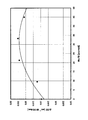
- the Mo content and the nitrogen content of the light shielding layer in which the sheet resistance value of the laminated film composed of the light shielding film and the etching mask film is 3.0 k ⁇ / ⁇ are plotted, and an approximate straight line is drawn.
- the film thicknesses of the antireflection layer of the light shielding film and the etching mask film in the laminated film are fixed values.
- the area on the right side including the plot of the approximate straight line indicates a region where a light shielding layer having a sheet resistance value of 3.0 k ⁇ / ⁇ or less can be formed.
- the ⁇ OD of the light shielding layer can be larger than 0.05 nm ⁇ 1 and the light shielding layer is 55 nm. It can be as follows. Further, in the case of a light shielding layer having a ⁇ OD of 0.06 nm ⁇ 1 or more, the nitrogen content can be 36 atomic% or less, and the thickness of the light shielding layer can be 50 nm or less.
- the nitrogen content can be 25 atomic% or less, and the thickness of the light shielding layer can be 43 nm or less. Further, in the case of a light shielding layer having ⁇ OD of 0.075 nm ⁇ 1 or more, the nitrogen content can be made 14 atomic% or less, and the thickness of the light shielding layer can be made 40 nm or less.
- the molybdenum content is more than 25 atomic% and ⁇ OD
- the molybdenum content is 24 atomic% or more
- the molybdenum content is 17 atomic% or more.
- the molybdenum content is preferably 9 atomic% or more.
- a light-shielding layer made of a MoSi film or a MoSiN film has a problem that when the content of molybdenum is large, chemical resistance and cleaning resistance (particularly alkali cleaning and hot water cleaning) are lowered. Therefore, the content of molybdenum in the MoSi film or MoSiN film is preferably set to 40 atomic% or less, which is a content that can ensure the minimum necessary chemical resistance and cleaning resistance when used as a photomask. As is apparent from FIGS.
- the light shielding performance of the light shielding layer made of the MoSi film or the MoSiN film reaches a predetermined value as the molybdenum content increases.
- the molybdenum content is preferably 40 atomic% or less from the viewpoint of cost.
- the etching rate in dry etching with a fluorine-based gas is relatively higher than the composition outside the range of the present invention. 2) Compared with the case where the Mo content in the light shielding layer is less than 9 atomic%, the conductivity necessary for electron beam drawing exposure can be ensured.
- the etching mask film preferably contains at least one of nitrogen and oxygen and carbon in addition to chromium (Configuration 4).
- etching resistance when the light shielding film is etched with a fluorine-based gas can be increased.
- the light shielding film is configured to obtain conductivity.
- the carbon content of the etching mask film is preferably 5 atomic% or more and 20 atomic% or less.
- the etching rate required in the present invention can be obtained in the etching mask film.
- the etching mask film has a chromium content of 35 atomic% or less and includes at least one of nitrogen and oxygen (Configuration 3).
- the etching rate with respect to chlorine-type gas improves, so that Cr type
- the total content of oxygen and nitrogen in the etching mask film is preferably 40 atomic% or more, and more preferably 50 atomic% or more.
- the total content of oxygen and nitrogen in the etching mask film is 40 atomic% or more, the required CD uniformity can be easily obtained.
- the Cr-based material film is dry-etched using the resist pattern as a mask, a global loading phenomenon occurs due to the density of the transfer pattern.
- oxygen plasma in the etching gas is generated in a region with a high resist coverage on the Cr-based material film (a region with a low exposure rate of the Cr-based material film. For example, a region with a relatively sparse pattern).
- the consumption amount is relatively large, and the etching rate of the Cr-based material film tends to be relatively slow.
- the consumption of oxygen plasma in the etching gas is relatively high.
- the etching rate of the Cr-based material film tends to be relatively high. This phenomenon is a common problem in Cr-based material films, and the same can be said for Cr-based etching mask films.
- the etching mask film may be formed of a material mainly containing any one of chromium oxycarbonitride (CrOCN), chromium oxide carbide (CrOC), chromium oxynitride (CrON), and chromium nitride (CrN). preferable.
- CrOCN chromium oxycarbonitride
- CrOC chromium oxide carbide
- CrON chromium oxynitride
- CrN chromium nitride
- chromium oxycarbonitride and chrome oxide are preferable.
- the film structure of the etching mask film is often a single layer made of the above film material, but may be a multi-layer structure.
- the multi-layer structure can be a multi-layer structure formed in stages with different compositions or a film structure in which the composition is continuously changed.
- the etching mask film is It is chromium oxycarbonitride or chromium oxycarbide, Using a chromium target, using a mixed gas containing at least “CO 2 gas, N 2 gas and rare gas” or “CO 2 gas and rare gas” (selecting a gas system having low hysteresis), and It is preferable to form a film under conditions near the start of transition from the metal mode to the reaction mode, or near the reaction mode. This is because a film having a fast etching rate can be stably produced in DC sputtering. Specifically, as shown in FIG.
- the metal mode is a region where a high voltage (eg, 330 to 350 V) is maintained (region where Cr is ion-sputtered by Ar), the transition region is a region where the voltage suddenly drops, and the reaction mode is a region after the sudden drop of the suddenly dropped voltage ( This refers to the region where the suddenly dropped voltage of 290 to 310 V is maintained (the region where the gas is activated and exhibits reactivity).
- the metal mode is a region of 0 to 30 sccm in FIG. 3 (1), a region of 0 to 25 sccm in FIG. 3 (2), and a region of 0 to 32 sccm in FIG. 3 (3).
- the transition region is a region of 35-50 sccm in the increase mode in FIG.
- the reaction region is a region of 50 to 35 sccm in the decrease mode in FIG. 3 (1), a region of 50 to 35 sccm in the decrease mode in FIG. 3 (2), and a region of 48 to 32 sccm in the decrease mode in FIG. .
- a chromium film having a very low degree of oxidation and nitridation is formed.
- a chromium film having a high degree of oxidation and nitridation is formed, and an intermediate mode between the metal mode and the reaction mode (a mode between the metal mode and the reaction mode).
- the conditions are not stable and are not normally used.
- There are various gas systems for oxidizing and nitriding chromium but as shown in FIG. 3 (3), when a gas system with large hysteresis (NO gas + noble gas) is used, the chromium oxidized and nitrided by DC sputtering is used. It is difficult to stably form a film with low defects in the reaction mode. The same applies to the case of using O 2 gas + rare gas.
- FIG. 3 (3) when a gas system with large hysteresis (NO gas + noble gas) is used, the chromium oxidized and nitrided by DC sputtering is used. It is difficult to stably form a film with low defects in the reaction mode. The same applies to the
- FIG. 3 (1) and FIG. 3 (2) when a gas system with small hysteresis is used (in FIG. 3 (1), “CO 2 gas + rare gas” is used, and FIG. 2) “CO 2 gas + N 2 gas + rare gas” is used, and chromium that has been oxidized and nitrided by DC sputtering is in a reaction mode (in FIG. 3A, a reduced mode region of 40-30 sccm, FIG. ) Can be stably formed with low defects in the reduced mode region of 35 to 25 sccm), and the oxidized and nitrided chromium obtained can produce a film with a high etching rate.
- the etching mask film is a resist film formed thereon and processed using a resist film having a thickness of 100 nm or less,
- the etching mask film has a thickness of 5 nm to 20 nm,
- the light-shielding film includes an aspect in which the film thickness is 60 nm or less (Configuration 5).
- the film thickness of the resist film is 100 nm or less.
- the Cr-based etching mask film has a thickness of 5 nm or more and 20 nm or less, and the light shielding film has a thickness of 60 nm or less.
- the resist film has a thickness of 75 nm or less, and A mode in which the film thickness of the etching mask film is 5 nm or more and 15 nm or less is included (Configuration 6).
- the film thickness of the resist film is 75 nm or less from the viewpoint of reducing the LER of the resist pattern.
- the Cr-based etching mask film preferably has a thickness of 5 nm or more and 15 nm or less.
- the resist film has a thickness of 65 nm or less, and A mode in which the film thickness of the etching mask film is 5 nm or more and 10 nm or less is included (Configuration 7).
- the film thickness of the resist film is 65 nm or less. This is because the Cr-based etching mask film preferably has a thickness of 5 nm or more and 10 nm or less.
- the light shielding layer includes an aspect in which the light shielding layer is formed of a material made of molybdenum and silicon, or a material made of molybdenum, silicon, and nitrogen (Configuration 8).
- the light shielding film includes at least a low reflection layer from the light transmitting substrate side, a light shielding layer formed in contact with the low reflection layer, and an antireflection layer formed in contact with the light shielding layer. It consists of three layers,
- the light shielding layer is a material composed of molybdenum and silicon, and the molybdenum content is 9 atomic% or more and 40 atomic% or less,
- the antireflection layer is made of a material containing molybdenum and silicon and at least one of oxygen and nitrogen
- the low reflection layer includes an aspect made of a material containing molybdenum and silicon and at least one of oxygen and nitrogen.
- the light shielding layer (MoSi film) made of molybdenum and silicon is made of a light shielding layer substantially composed of molybdenum and silicon (a metallic film substantially free of oxygen, nitrogen, etc., made of molybdenum silicide metal). Including the film).
- a mode in which these elements are included within a range in which the effects of the present invention can be obtained both oxygen and nitrogen are each less than 5 atomic% of the components in the light shielding layer) is included. .
- the light shielding layer made of the MoSi film may contain other elements (carbon, helium, hydrogen, argon, xenon, etc.) as long as the above characteristics and effects are not impaired.
- the light shielding layer made of the MoSi film preferably has a thickness of 24 nm or more, and more preferably 27 nm or more.
- the layer thickness is preferably less than 40 nm, more preferably 35 nm or less. Furthermore, in order to ensure conductivity with the light shielding film, the ratio of the light shielding layer to the light shielding film is preferably 0.4 or more and 0.6 or less.
- the light shielding film is composed of two layers including a light shielding layer from the translucent substrate side and an antireflection layer formed on and in contact with the light shielding layer,
- the light shielding layer is a material composed of molybdenum, silicon, and nitrogen, and the molybdenum content is 9 atomic% or more and 40 atomic% or less
- the antireflection layer includes an aspect made of a material containing molybdenum and silicon and at least one of oxygen and nitrogen (Configuration 9). With the above configuration, antireflection (for example, 30% or less) on the front surface side and the back surface side (translucent substrate side) of the light shielding film is achieved.
- a light shielding layer (MoSiN film) made of molybdenum, silicon, and nitrogen refers to a light shielding layer (including a film made of a molybdenum silicide compound) substantially composed of molybdenum, silicon, and nitrogen.
- the film does not substantially contain oxygen, for the same reason as the MoSi film, there is an aspect in which oxygen is contained within a range in which the effect of the present invention can be obtained (the oxygen component in the light shielding layer is less than 5 atomic%). included.
- the light shielding layer made of the MoSiN film may contain other elements (carbon, helium, hydrogen, argon, xenon, etc.) as long as the above characteristics and effects are not impaired.
- the light shielding layer can have a back surface antireflection function and the light shielding film can have a two-layer structure. Further, the etching rate of the light shielding layer can be made slower than that of the MoSi film containing no nitrogen in the light shielding layer. Therefore, compared with a three-layered light shielding film having a light shielding layer made of a MoSi film, the etching rate difference between the antireflection layer and the light shielding layer can be eliminated, and the cross-sectional shape of the pattern can be improved. Become.
- the content of nitrogen in the MoSiN film is preferably less than 40 atomic%.
- the thickness of the light shielding layer can be reduced, and the light shielding film can be 60 nm or less.
- the light shielding layer made of a MoSiN film preferably has a thickness of 36 nm or more, and more preferably 42 nm or more.
- the layer thickness is desirably 55 nm or less, and more desirably 52 nm or less.
- the ratio of the light shielding layer made of the MoSiN film to the light shielding film is preferably 0.6 or more and 0.9 or less.
- the light shielding layer can freely control tensile stress and compressive stress by Ar gas pressure, He gas pressure, and heat treatment.
- the film stress of the light shielding layer can be a tensile stress, it can be matched with the compressive stress of the antireflection layer (for example, MoSiON). That is, the stress of each layer constituting the light shielding film can be offset, and the film stress of the light shielding film can be reduced as much as possible (can be substantially zero).
- the antireflection layer in the present invention contains molybdenum and silicon and at least one of oxygen and nitrogen.
- the antireflection layer include MoSiON, MoSiO, MoSiN, MoSiOC, and MoSiOCN.
- MoSiO and MoSiON are preferable from the viewpoint of chemical resistance and heat resistance, and MoSiON is preferable from the viewpoint of blanks defect quality.
- the content of Mo in the antireflection layer is preferably less than 10 atomic%.
- Mo when the Mo content is too small, abnormal discharge during DC sputtering becomes significant, and the frequency of occurrence of defects increases. Therefore, it is desirable that Mo is contained within a range that can be normally sputtered. Depending on other film formation techniques, film formation may be possible without containing Mo.
- the content ratio of molybdenum and silicon in the antireflection layer is preferably 1: 6 or more, 1:16 or more is still more preferable, and 1:20 or more is more preferable.
- a photomask is repeatedly used, atmospheric oxygen (O 2 ), water (H 2 O), ozone (O 3 ) generated by reaction of atmospheric oxygen (O 2 ) with an ArF excimer laser, etc.
- O 2 atmospheric oxygen
- H 2 O water
- O 3 ozone
- the content ratio of molybdenum and silicon in the antireflection layer is preferably the above ratio in order to reduce the Mo content of the light shielding film as much as possible.
- the antireflection layer is preferably oxidized in order to obtain a predetermined surface reflectance. In this case, the etching time of the antireflection layer tends to be long. Therefore, by reducing the Mo content of the antireflection layer, the etching time of the antireflection layer can be shortened when the light shielding film is etched using the Cr-based etching mask film as a mask.
- the antireflection layer contains nitrogen and / or oxygen
- the total content of nitrogen and oxygen is 30 atomic% or more, preferably 45 atomic% or more.
- the total content of nitrogen and oxygen in the antireflection layer is preferably 60 atomic% or less.
- the antireflection layer preferably has a thickness of 5 nm to 20 nm, and more preferably 7 nm to 15 nm.
- the etching mask film is preferably a film that is removed when a photomask is manufactured (Configuration 10). Since the light shielding film itself has an antireflection function, when the photomask is manufactured, the etching mask film on the light shielding film can be finally peeled off.
- a dry etching gas composed of a chlorine-based gas or a mixed gas containing a chlorine-based gas and an oxygen gas for the dry etching of the Cr-based etching mask film.
- the dry etching rate can be increased by performing dry etching using the above-mentioned dry etching gas on a Cr-based etching mask film made of a material containing chromium and elements such as oxygen and nitrogen. This is because the dry etching time can be shortened and a light-shielding film pattern having a good cross-sectional shape can be formed.
- the chlorine-based gas used for dry etching gas for example, Cl 2, SiCl 4, HCl , CCl 4, CHCl 3 , and the like.
- the dry etching of the MoSi-based light-shielding film for example, fluorine-based gas such as SF 6 , CF 4 , C 2 F 6 , CHF 3 , and these, and He, H 2 , N 2 , Ar, C 2 H 4, a mixed gas such as O 2, or Cl 2, CH 2 Cl 2 or the like chlorine based gas or can be used such as He, H 2, N 2, Ar, a mixed gas such as C 2 H 4 .
- fluorine-based gas such as SF 6 , CF 4 , C 2 F 6 , CHF 3 , and these, and He, H 2 , N 2 , Ar, C 2 H 4
- a mixed gas such as O 2, or Cl 2, CH 2 Cl 2 or the like chlorine based gas or can be used such as He, H 2, N 2, Ar, a mixed gas such as C 2 H 4 .
- examples of the substrate include a synthetic quartz substrate, a CaF 2 substrate, a soda lime glass substrate, a non-alkali glass substrate, a low thermal expansion glass substrate, and an aluminosilicate glass substrate.
- the photomask blank of the present invention includes an embodiment having a resist film formed on the etching mask film (Configuration 11).
- the photomask of the present invention is produced using the photomask blank according to the present invention (Configuration 12). As a result, the same effects as described in configurations 1 to 10 can be obtained.
- the method for producing a photomask of the present invention comprises: Preparing the photomask blank according to the present invention, Using the resist pattern formed on the etching mask film as a mask, pattern etching is performed by performing dry etching using a chlorine-based gas containing oxygen on the etching mask film, Using the pattern formed on the etching mask film as a mask, pattern transfer is performed by performing dry etching using a fluorine-based gas on the light shielding film, After the pattern transfer to the light shielding film, the etching mask film is removed by dry etching using a chlorine-based gas containing oxygen (Configuration 13). As a result, the same effects as described in configurations 1 to 10 can be obtained.
- the semiconductor device manufacturing method of the present invention is performed by transferring the photomask pattern according to the present invention (Configuration 14).
- the photomask blank includes a binary photomask blank that does not use the phase shift effect and a mask blank with a resist film.
- the photomask blank includes a halftone type phase shift mask blank provided with a phase shift film between the translucent substrate and the light shielding film.
- the phase shift film can have the same configuration as the conventional one, and is formed of a material made of, for example, MoSiN or MoSiON.
- an etching stopper film having etching resistance to the light shielding film and the phase shift film may be provided between the light transmitting substrate and the light shielding film or between the phase shift film and the light shielding film.
- the etching stopper film is formed of a Cr-based material film like the etching mask film because the etching mask film can be peeled off simultaneously when the etching stopper film is etched.
- the photomask includes a binary photomask that does not use the phase shift effect, and among the phase shift masks that use the phase shift effect, a halftone phase shift mask, a Levenson type phase shift mask, and an enhancer mask are included. It is.
- the photomask includes a reticle.
- the photomask to which exposure light having a wavelength of 200 nm or less is applied includes a photomask for ArF excimer laser exposure.
- membrane such as a light shielding film and an etching mask film
- the film forming method and the film forming apparatus are not particularly limited, and other types of sputtering apparatuses such as an RF magnetron sputtering apparatus may be used.
- Example (1-1) (Production of photomask blank) A synthetic quartz substrate having a size of 6 inches square and a thickness of 0.25 inches is used as the translucent substrate 1, and a MoSiON film 11 (back surface antireflection layer) and MoSi (light shielding layer) are formed on the translucent substrate 1 as the light shielding film 10. Layer) 12 and a MoSiON film (surface antireflection layer) 13 were formed (FIG. 1).
- the optical density (OD) of the light-shielding film 10 was 3 at a wavelength of 193 nm of ArF excimer laser exposure light.
- the substrate was heated (annealed) at 450 ° C. for 30 minutes.
- the film was formed under the condition of the transition from the metal mode to the reaction mode (nearly) (CO 2 flow rate of 37 sccm) at a power of 1.8 kW and a voltage of 334 V (see FIG. 3 (2)). ), A CrOCN film (Cr: 33 atomic%, O: 38.9 atomic%, C: 11.1 atomic%, N: 17 atomic%) was formed with a film thickness of 5 nm. At this time, by annealing the CrOCN film at a temperature lower than the annealing temperature of the MoSi light-shielding film, the stress of the CrOCN film is as low as possible without affecting the film stress of the MoSi light-shielding film (preferably substantially zero film stress).
- a chemically amplified positive resist 50 (PRL009: manufactured by Fuji Film Electronics Materials Co., Ltd.) for electron beam drawing (exposure) is applied by spin coating so that the film thickness becomes 100 nm.
- PRL009 manufactured by Fuji Film Electronics Materials Co., Ltd.
- the resist film 50 is developed with a predetermined developer and then resist is developed.
- a pattern 50a was formed (FIG. 2 (2)).
- etching mask film 20 was performed using the resist pattern 50a as a mask (FIG. 2 (3)).
- the remaining resist pattern 50a was peeled off with a chemical solution.
- the etching mask film pattern 20a was dry-etched using a mixed gas of SF 6 and He to form the light shielding film pattern 10a (FIG. 2 (4)).
- the etching mask film pattern 20a was peeled off by dry etching with a mixed gas of Cl 2 and O 2 (FIG.
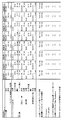
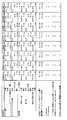
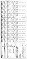
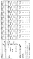
- FIG. 4 shows the configuration of the photomask blank used in Example (1-1) (characteristics such as light shielding film, etching mask film, resist film material and film thickness).
- the processing characteristics of the photomask blank used in Example (1-1) (the resist film thickness after dry etching of the etching mask film, the film thickness of the etching mask film after dry etching of the light shielding film, CD linearity, CD uniformity) Resist film resolution (LER (Line Edge Roughness) below 40 nm, resist collapse, etc.), etching mask film LER (Line Edge Roughness)), and resolution of light-shielding film pattern in the obtained photomask
- LER Line Edge Roughness
- LER Line Edge Roughness
- Example (1-2) is the same as Example (1-1) except that the film thickness of the CrOCN film as the etching mask film 20 is changed from 5 nm to 10 nm in Example (1-1). is there.
- FIG. 4 shows the configuration of the photomask blank used in Example (1-2), its processing characteristics, and the resolution of the light shielding film pattern in the obtained photomask.
- Example (1-3) is the same as Example (1-1) except that the film thickness of the CrOCN film as etching mask film 20 is changed from 5 nm to 15 nm in Example (1-1). is there.
- FIG. 4 shows the configuration of the photomask blank used in Example (1-3), its processing characteristics, and the resolution of the light-shielding film pattern in the obtained photomask.
- Example (1-4) is the same as Example (1-1) except that the film thickness of the CrOCN film as etching mask film 20 is changed from 5 nm to 20 nm in Example (1-1). is there.
- FIG. 4 shows the configuration of the photomask blank used in Example (1-4), its processing characteristics, and the resolution of the light-shielding film pattern in the obtained photomask.
- Examples (1-5) to (1-8) the CrOCN film as the etching mask film 20 is replaced with a CrOC film in Examples (1-1) to (1-4), and film formation is performed under the following conditions. This is the same as the examples (1-1) to (1-4) except that the Cr content in the CrOC film is 35 atomic%.
- FIG. 4 shows the configuration of the photomask blank used in Examples (1-5) to (1-8), its processing characteristics, and the resolution of the light shielding film pattern in the obtained photomask.
- Examples (1-9) to (1-12) the CrOCN film as the etching mask film 20 is changed to a CrON film in Examples (1-1) to (1-4), and film formation is performed under the following conditions. Except what has been done, the procedure is the same as those in Examples (1-1) to (1-4).
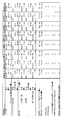
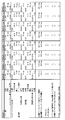
- FIG. 5 shows the configuration of the photomask blank used in Examples (1-9) to (1-12), its processing characteristics, and the resolution of the light-shielding film pattern in the obtained photomask.
- Reference examples (1-13) to (1-16) In Reference Examples (1-13) to (1-16), the CrOCN film as the etching mask film 20 is changed to a CrN film in Examples (1-1) to (1-4), and the film is formed under the following conditions. Except what was done, the procedure is the same as in Examples (1-1) to (1-4).
- FIG. 5 shows the configuration of the photomask blank used in Reference Examples (1-13) to (1-16), its processing characteristics, and the resolution of the light-shielding film pattern in the obtained photomask.
- Example (1-17) In Example (1-17), film formation was performed on MoSi (light shielding layer) 12 in light shielding film 10 under the following conditions in Example (1-1), and the film thickness of MoSi (light shielding layer) 12 was changed. Except that the Si content in the MoSi (light-shielding layer) 12 was changed and the total film thickness of the light-shielding film 10 was changed, the same as in Example 1-1.
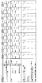
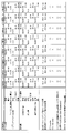
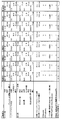
- FIG. 6 shows the configuration of the photomask blank used in Example (1-17), its processing characteristics, and the resolution of the light-shielding film pattern in the obtained photomask.
- Example (1-18) In Example (1-18), film formation was performed on MoSi (light shielding layer) 12 in light shielding film 10 under the following conditions in Example (1-1), and the film thickness of MoSi (light shielding layer) 12 was changed. The same as Example 1-1 except that the Si content in the MoSi (light shielding layer) 12 was changed and the total thickness of the light shielding film 10 was changed.
- FIG. 6 shows the configuration of the photomask blank used in Example (1-18), its processing characteristics, and the resolution of the light-shielding film pattern in the obtained photomask.
- Example (1-19) In Example (1-19), film formation was performed on MoSi (light shielding layer) 12 in light shielding film 10 under the following conditions in Example (1-1), and the film thickness of MoSi (light shielding layer) 12 was changed. The same as Example 1-1 except that the Si content in the MoSi (light shielding layer) 12 was changed and the total thickness of the light shielding film 10 was changed.
- membrane Mo: 33 atomic%, Si: 67 atomic%) which consists of silicon was formed with the film thickness of 29 nm, and the total film thickness of the light shielding film 10 was 51 nm.
- FIG. 6 shows the configuration of the photomask blank used in Example (1-19), its processing characteristics, and the resolution of the light-shielding film pattern in the obtained photomask.
- Example (1-20) In Example (1-20), film formation was performed on MoSi (light shielding layer) 12 in light shielding film 10 under the following conditions in Example (1-1), and the film thickness of MoSi (light shielding layer) 12 was changed. The same as Example 1-1 except that the Si content in the MoSi (light shielding layer) 12 was changed and the total thickness of the light shielding film 10 was changed.
- FIG. 6 shows the configuration of the photomask blank used in Example (1-20), its processing characteristics, and the resolution of the light-shielding film pattern in the obtained photomask.
- Example (1-21) In Example (1-21), the MoSiON film 11 (back surface antireflection layer) was not formed for the light shielding film 10 in Example (1-1), the MoSi (light shielding layer) 12 in the light shielding film 10, and Regarding the MoSiON film (surface antireflection layer) 13, the film was formed under the following conditions, the MoSi (light shielding layer) 12 was changed to MoSiN (light shielding layer) 12, and the film thickness and the Si content in the film were changed. Except that the film thickness of the MoSiON film (surface antireflection layer) 13 was changed and the total film thickness of the light shielding film 10 was changed, the same as in Example 1-1.
- the MoSiN (light shielding layer) 12 in the light shielding film 10 is a film made of molybdenum, silicon, and nitrogen (Mo: 9 atomic%, Si: 72.8 atomic%, N: 18.2 atomic%) with a film thickness of 52 nm. did.
- the MoSiON film (surface antireflection layer) 13 in the light shielding film 10 is a film made of molybdenum, silicon, oxygen, and nitrogen (Mo: 1.6 atomic%, Si: 38.8 atomic%, O: 18.8 atomic%, N: 40.8 atomic%) was formed with a film thickness of 8 nm.
- the total film thickness of the light shielding film 10 was 60 nm.
- the optical density (OD) of the light-shielding film 10 was 3 at a wavelength of 193 nm of ArF excimer laser exposure light.
- FIG. 6 shows the configuration of the photomask blank used in Example (1-21), its processing characteristics, and the resolution of the light-shielding film pattern in the obtained photomask.
- Example (1-22) In Example (1-22), MoSiON film 11 (back surface antireflection layer) was not formed on light shielding film 10 in Example (1-1), MoSi (light shielding layer) 12 in light shielding film 10 and Regarding the MoSiON film (surface antireflection layer) 13, the film was formed under the following conditions, the MoSi (light shielding layer) 12 was changed to MoSiN (light shielding layer) 12, and the film thickness and the Si content in the film were changed. Except that the film thickness of the MoSiON film (surface antireflection layer) 13 was changed and the total film thickness of the light shielding film 10 was changed, the same as in Example 1-1.
- the MoSiN (light-shielding layer) 12 in the light-shielding film 10 is a film made of molybdenum, silicon, and nitrogen (Mo: 18 atomic%, Si: 63.8 atomic%, N: 18.2 atomic%) with a film thickness of 50 nm. did.
- the MoSiON film (surface antireflection layer) 13 in the light shielding film 10 is a film made of molybdenum, silicon, oxygen, and nitrogen (Mo: 1.6 atomic%, Si: 38.8 atomic%, O: 18.8 atomic%, N: 40.8 atomic%) was formed with a film thickness of 10 nm.
- the total film thickness of the light shielding film 10 was 60 nm.
- the optical density (OD) of the light-shielding film 10 was 3 at a wavelength of 193 nm of ArF excimer laser exposure light.
- FIG. 6 shows the configuration of the photomask blank used in Example (1-22), its processing characteristics, and the resolution of the light-shielding film pattern in the obtained photomask.
- Example (1-23) In Example (1-23), the MoSiON film 11 (back surface antireflection layer) was not formed for the light shielding film 10 in Example (1-1), the MoSi (light shielding layer) 12 in the light shielding film 10, and Regarding the MoSiON film (surface antireflection layer) 13, the film was formed under the following conditions, the MoSi (light shielding layer) 12 was changed to MoSiN (light shielding layer) 12, and the film thickness and the Si content in the film were changed. Except that the film thickness of the MoSiON film (surface antireflection layer) 13 was changed and the total film thickness of the light shielding film 10 was changed, the same as in Example 1-1.
- the MoSiN (light shielding layer) 12 in the light shielding film 10 is a film made of molybdenum, silicon, and nitrogen (Mo: 30 atomic%, Si: 51.8 atomic%, N: 18.2 atomic%) with a film thickness of 45 nm. did.
- the MoSiON film (surface antireflection layer) 13 in the light shielding film 10 is a film made of molybdenum, silicon, oxygen, and nitrogen (Mo: 1.6 atomic%, Si: 38.8 atomic%, O: 18.8 atomic%, N: 40.8 atomic%) was formed with a film thickness of 15 nm.
- the total film thickness of the light shielding film 10 was 60 nm.
- the optical density (OD) of the light-shielding film 10 was 3 at a wavelength of 193 nm of ArF excimer laser exposure light.
- FIG. 6 shows the configuration of the photomask blank used in Example (1-23), its processing characteristics, and the resolution of the light-shielding film pattern in the obtained photomask.
- Example (1-24) In Example (1-24), the MoSiON film 11 (back surface antireflection layer) was not formed on the light shielding film 10 in Example (1-1), the MoSi (light shielding layer) 12 in the light shielding film 10 and Regarding the MoSiON film (surface antireflection layer) 13, the film was formed under the following conditions, the MoSi (light shielding layer) 12 was changed to MoSiN (light shielding layer) 12, and the film thickness and the Si content in the film were changed. Except that the film thickness of the MoSiON film (surface antireflection layer) 13 was changed and the total film thickness of the light shielding film 10 was changed, the same as in Example 1-1.
- the MoSiN (light-shielding layer) 12 in the light-shielding film 10 is a film made of molybdenum, silicon, and nitrogen (Mo: 40 atomic%, Si: 41.8 atomic%, N: 18.2 atomic%) with a film thickness of 42 nm. did.
- the MoSiON film (surface antireflection layer) 13 in the light shielding film 10 is a film made of molybdenum, silicon, oxygen, and nitrogen (Mo: 1.6 atomic%, Si: 38.8 atomic%, O: 18.8 atomic%, N: 40.8 atomic%) was formed with a film thickness of 18 nm.
- the total film thickness of the light shielding film 10 was 60 nm.
- the optical density (OD) of the light-shielding film 10 was 3 at a wavelength of 193 nm of ArF excimer laser exposure light.
- FIG. 6 shows the configuration of the photomask blank used in Example (1-24), its processing characteristics, and the resolution of the light-shielding film pattern in the obtained photomask.
- Example (1-25) In Example (1-25), the MoSiON film 11 (back surface antireflection layer) was not formed on the light shielding film 10 in Example (1-1), the MoSi (light shielding layer) 12 in the light shielding film 10 and Regarding the MoSiON film (surface antireflection layer) 13, the film was formed under the following conditions, the MoSi (light shielding layer) 12 was changed to MoSiN (light shielding layer) 12, and the film thickness and the Si content in the film were changed. Except that the film thickness of the MoSiON film (surface antireflection layer) 13 was changed and the total film thickness of the light shielding film 10 was changed, the same as in Example 1-1.
- the MoSiN (light-shielding layer) 12 in the light-shielding film 10 is a film made of molybdenum, silicon, and nitrogen (Mo: 14.7 atomic%, Si: 56.2 atomic%, N: 29.1 atomic%) having a thickness of 50 nm.
- the MoSiON film (surface antireflection layer) 13 in the light shielding film 10 is a film made of molybdenum, silicon, oxygen, and nitrogen (Mo: 2.6 atomic%, Si: 57.1 atomic%, O: 15.9 atomic%, N: 24.4 atomic%) was formed with a film thickness of 10 nm.
- the total film thickness of the light shielding film 10 was 60 nm.
- the optical density (OD) of the light-shielding film 10 was 3 at a wavelength of 193 nm of ArF excimer laser exposure light.
- FIG. 6 shows the configuration of the photomask blank used in Example (1-25), its processing characteristics, and the resolution of the light-shielding film pattern in the obtained photomask.
- Examples (2-1) to (2-12), Reference Examples (2-13) to (2-16) Examples (2-1) to (2-12) and Reference Examples (2-13) to (2-16) were used in Examples (1-1) to (1-12) and Reference Example (1-13).
- a chemically amplified positive resist 50 for electron beam drawing (exposure) PRL009: manufactured by Fuji Film Electronics Materials
- PRL-009 manufactured by Fuji Film Electronics Materials
- SSL- chemically amplified positive resist 50 for electron beam drawing (exposure)
- 08 Same as Examples (1-1) to (1-12) and Reference Examples (1-13) to (1-16) except that it was changed to Fuji Film Electronics Materials Co., Ltd.
- Example (2-17) the CrOCN film as the etching mask film 20 was formed under the following conditions in Example (2-4), and the Cr content in the CrOCN film was set to 40 atomic%. Except for this point, this example is the same as Example (2-4). Specifically, the CrOCN film as the etching mask film 20 uses a chromium target, and Ar, CO 2 , N 2, and He are mixed with a sputtering gas pressure of 0.2 Pa (gas flow ratio Ar: CO 2 : N 2 : He).
- Example 2-18 In Example (2-18), the CrOCN film as the etching mask film 20 was formed under the following conditions in Example (2-4), and the Cr content in the CrOCN film was set to 45 atomic%. Except for this point, this example is the same as Example (2-4).
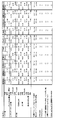
- FIG. 9 shows the configuration of the photomask blank used in Example (2-18), its processing characteristics, and the resolution of the light-shielding film pattern in the obtained photomask.
- Example 9 shows the configuration of the photomask blank used in Example (2-19), its processing characteristics, and the resolution of the light-shielding film pattern in the obtained photomask.
- Example 2-21 In Example (2-21), the CrON film as the etching mask film 20 was formed under the following conditions in Example (2-12), and the Cr content in the CrON film was 40 atomic%. Except for this point, this example is the same as Example (2-12).
- the film was formed with a DC power supply of 1.8 kW, and a CrON film (Cr content in the film: 40 atomic%) was formed to a thickness of 20 nm.
- FIG. 9 shows the configuration of the photomask blank used in Example (2-21), its processing characteristics, and the resolution of the light-shielding film pattern in the obtained photomask.
- Example 9 shows the configuration of the photomask blank used in Example (2-22), its processing characteristics, and the resolution of the light-shielding film pattern in the obtained photomask.
- Example (2-23) In Example (2-23), the CrN film as the etching mask film 20 was formed under the following conditions in Reference Example (2-16) so that the Cr content in the CrN film was 40 atomic%. Except for this, it is the same as Reference Example (2-16).
- FIG. 9 shows the configuration of the photomask blank used in Example (2-23), its processing characteristics, and the resolution of the light-shielding film pattern in the obtained photomask.
- FIG. 9 shows the configuration of the photomask blank used in Example (2-24), its processing characteristics, and the resolution of the light-shielding film pattern in the obtained photomask.
- Examples (3-1) to (3-12), Reference Examples (3-13) to (3-16) Examples (3-1) to (3-12) and Reference Examples (3-13) to (3-16) are referred to as Examples (1-1) to (1-12) and Reference Example (1-13).
- the thickness of the chemically amplified positive resist 50 (PRL009: manufactured by Fuji Film Electronics Materials) for electron beam drawing (exposure) was changed from 100 nm to 90 nm, and the resist pattern was changed accordingly.
- FIG. 12 shows the configuration of the photomask blank used in Examples (3-17) to (3-24), its processing characteristics, and the resolution of the light shielding film pattern in the obtained photomask.
- Examples (4-1) to (4-9), Reference Examples (4-10) to (4-12) Examples (4-1) to (4-9) and Reference Examples (4-10) to (4-12) are examples (1-1) to (1-3) and Example (1-5).
- Examples (1-9) to (1-11) and Reference Examples (1-13) to (1-15) a chemically amplified positive resist 50 for electron beam drawing (exposure) (PRL009: manufactured by Fuji Film Electronics Materials Co., Ltd.)
- PRL009 manufactured by Fuji Film Electronics Materials Co., Ltd.
- the film thickness was changed from 100 nm to 75 nm, and accordingly, the ratio (aspect ratio) of the resist pattern line width (40 nm) to the resist film thickness of 75 nm was 1.
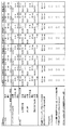
- Structure of photomask blank used in Examples (4-1) to (4-9) and Reference Examples (4-10) to (4-12), processing characteristics thereof, and light-shielding film in the obtained photomask The resolution of the pattern is shown in FIGS. Examples (4-13) to (4-20)
- Examples (4-13) to (4-20) are the same as in Examples (2-17) to (2-24), but are chemically amplified positive resist 50 (SVL-08: Fuji Film) for electron beam drawing (exposure).
- FIG. 14 shows the configuration of the photomask blank used in Examples (4-13) to (4-20), its processing characteristics, and the resolution of the light-shielding film pattern in the obtained photomask.
- Examples (5-1) to (5-6), Reference Examples (5-7) to (5-8) Examples (5-1) to (5-6) and Reference Examples (5-7) to (5-8) are examples (1-1) to (1-2) and Example (1-5).
- Examples (1-9) to (1-10) and Reference Examples (1-13) to (1-14) a chemically amplified positive resist 50 for electron beam drawing (exposure) (PRL009: manufactured by Fuji Film Electronics Materials Co., Ltd.)
- PRL009 manufactured by Fuji Film Electronics Materials Co., Ltd.
- Structure of photomask blank used in Examples (5-1) to (5-6) and Reference Examples (5-7) to (5-8), its processing characteristics, and a light-shielding film in the obtained photomask The resolution of the pattern is shown in FIG. Examples (5-9) to (5-16)
- Examples (5-9) to (5-16) are the same as in Examples (2-17) to (2-24).
- Chemically amplified positive resist 50 for electron beam drawing (exposure) (SVL-08: Fuji Film) Electronics Materials Co., Ltd.) was changed to electron beam drawing (exposure) chemical amplification type positive resist 50 (PRL009: Fuji Film Electronics Materials Co., Ltd.), electron beam drawing (exposure) chemical amplification type positive resist 50
- the film thickness of the resist mask was changed to 65 nm, and the ratio of the resist pattern line width (40 nm) to the resist film thickness of 65 nm (aspect ratio) was changed to 1: 1.4. Is the same as Examples (2-17) to (2-24) except that the thickness is set to 10 nm.
- FIG. 16 shows the configuration of the photomask blank used in Examples (5-9) to (5-16), its processing characteristics, and the resolution of the light-shielding film pattern in the obtained photomask.
- Comparative Examples 1 and 2 Comparative Example 1 is the same as Example (2-1) except that in Example (2-1), the thickness of the CrOCN film as etching mask film 20 was changed from 5 nm to 4 nm.
- Comparative Example 2 is the same as Example (2-4) except that in Example (2-4), the thickness of the CrOCN film as etching mask film 20 was changed from 20 nm to 30 nm.
- FIG. 17 shows the configuration of the photomask blank used in Comparative Examples 1 and 2, its processing characteristics, and the resolution of the light shielding film pattern in the obtained photomask.
- Comparative Examples 3-4 the thickness of the chemically amplified positive resist 50 (PRL009: manufactured by Fuji Film Electronics Materials) for electron beam drawing (exposure) was changed from 100 nm to 120 nm in Example (1-4). Accordingly, this example is the same as Example (1-4) except that the ratio (aspect ratio) of the resist pattern line width (40 nm) to the resist film thickness 120 nm is changed to 1: 1.3.
- the film thickness of the chemically amplified positive resist 50 for electron beam drawing (exposure) (SVL-08: manufactured by Fuji Film Electronics Materials) in Example (2-4) was changed from 100 nm to 120 nm.
- FIG. 17 shows the configuration of the photomask blank used in Comparative Examples 3 to 4, its processing characteristics, and the resolution of the light shielding film pattern in the obtained photomask.
- FIG. 17 shows the configuration of the photomask blank used in Comparative Examples 5 to 7, its processing characteristics, and the resolution of the light shielding film pattern in the obtained photomask.
- FIG. 17 shows the configuration of the photomask blank used in Comparative Example 8, its processing characteristics, and the resolution of the light shielding film pattern in the obtained photomask.
- FIG. 18 shows the configuration of the photomask blank used in Comparative Example 9, its processing characteristics, and the resolution of the light-shielding film pattern in the obtained photomask.
- Comparative Example 10 is the same as Reference Example (2-16) except that CrN film as etching mask film 20 is changed to Cr film in Reference Example (2-16) and film formation is performed under the following conditions. is there. Specifically, the Cr film as the etching mask film 20 is formed in a metal mode by using a chromium target, Ar with a sputtering gas pressure of 0.2 Pa, a DC power supply of 1.8 kW, a voltage of 330 V, and the like. Then, pure chromium having a Cr content of 100 atomic% in the Cr film was formed to a thickness of 20 nm.
- FIG. 18 shows the configuration of the photomask blank used in Comparative Example 10, its processing characteristics, and the resolution of the light shielding film pattern in the obtained photomask.
- Comparative Example 11 is the same as Reference Example (1-16) except that CrN film as etching mask film 20 is changed to Cr film in Reference Example (1-16) and film formation is performed under the following conditions. is there. Specifically, the Cr film as the etching mask film 20 is formed in a metal mode by using a chromium target, Ar with a sputtering gas pressure of 0.2 Pa, a DC power supply of 1.8 kW, a voltage of 330 V, and the like. Then, pure chromium having a Cr content of 100 atomic% in the Cr film was formed to a thickness of 20 nm.
- FIG. 18 shows the configuration of the photomask blank used in Comparative Example 11, its processing characteristics, and the resolution of the light-shielding film pattern in the obtained photomask.
- Comparative Example 12 was the same as in Example (1-21) except that film formation was performed on the MoSi (light-shielding layer) 12 in the light-shielding film 10 under the following conditions, and the film thickness and the Si content in the film were changed. The same as Example (1-21) except that the total film thickness of the light-shielding film 10 was changed.
- the MoSiN (light-shielding layer) 12 in the light-shielding film 10 is a film made of molybdenum, silicon, and nitrogen (Mo: 6 atomic%, Si: 75.8 atomic%, N: 18.2 atomic%) with a film thickness of 62 nm. did.
- the total film thickness of the light shielding film 10 was 70 nm.
- the optical density (OD) of the light-shielding film 10 was 3 at a wavelength of 193 nm of ArF excimer laser exposure light.
- FIG. 18 shows the configuration of the photomask blank used in Comparative Example 12, its processing characteristics, and the resolution of the light-shielding film pattern in the obtained photomask.
- Comparative Example 13 In Comparative Example 13, the CrN film as the etching mask film 20 in Reference Example (4-11) was formed under the following conditions, and the Cr content in the CrN film was changed from 50 atomic% to 90 atomic%. This is the same as Reference Example (4-11). Specifically, the CrN film as the etching mask film 20 uses a chromium target, Ar and N 2 are set to sputtering gas pressure 0.2 Pa (gas flow ratio Ar: N 2 : He18: 18: 32), and DC Film formation was performed in a metal mode with a power of 1.8 kW and a voltage of 335 V, and a CrN film (Cr content in the film: 90 atomic%) was formed to a thickness of 10 nm. FIG.
- Comparative Example 14 shows the configuration of the photomask blank used in Comparative Example 13, its processing characteristics, and the resolution of the light shielding film pattern in the obtained photomask.
- Comparative Example 14 In Comparative Example 14, the MoSi film (light-shielding layer) 12 in the light-shielding film 10 in Example (1-17) was formed under the following conditions, and the film thickness of the MoSi film (light-shielding layer) 12 was changed. The same as Example (1-17) except that the Si content in the film (light shielding layer) 12 was changed and the total film thickness of the light shielding film 10 was changed.
- a film made of molybdenum and silicon (Mo: 8 atomic%, Si: 92 atomic%) was formed with a film thickness of 38 nm, and the total film thickness of the light-shielding film 10 was 60 nm.
- FIG. 18 shows the configuration of the photomask blank used in Example (1-17), its processing characteristics, and the resolution of the light-shielding film pattern in the obtained photomask.
- the sheet resistance value of the laminated film composed of the light-shielding film and the etching mask film required in the electron beam drawing exposure is determined to be good if it is 3.0 k ⁇ / ⁇ or less.
- the sheet resistance value was measured based on a 4-terminal measurement method. In Examples (1-1) to (1-12), Reference Examples (1-13) to (1-16), and Examples (1-17) to (1-24), the dry etching of the etching mask film is performed.
- the film thickness of the resist varies in a range from a maximum of 93.6 nm (Example 1-9) to a minimum of 70.1 nm (Example 1-16), and the film thickness of the etching mask film after dry etching of the light shielding film However, it fluctuates in the range of a minimum of 3.1 nm (Example 1-21) to a maximum of 18.6 nm (Example 1-4).
- the sheet resistance value of only the light-shielding film and the sheet resistance value of the laminated film are 3.0 k ⁇ / ⁇ or less. The CD linearity and CD uniformity were also good.
- the resist film thickness after dry etching of the etching mask film is 92.7 nm at maximum (Example 2). ⁇ 9) to a minimum of 66.2 nm (Reference Example 2-16), and the thickness of the etching mask film after dry etching of the light shielding film is 3.6 nm (Example 2-1 etc.) It fluctuates in the range of up to 18.6 nm (Example 2-4 etc.).
- the resolution of the resist film (LER below 40 nm, resist collapse, etc.) is good.
- the LER of the etching mask film was good, and the resolution of the light-shielding film pattern in the obtained photomask was less than 40 nm.
- the sheet resistance value of only the light-shielding film and the sheet resistance value of the laminated film satisfy 3.0 k ⁇ / ⁇ or less, and the CD linearity and CD uniformity are also good. It was.
- the sheet resistance value of the laminated film satisfied 3.0 k ⁇ / ⁇ or less, but the Cr content in the etching mask film was relatively high at 50 atomic%.
- the resist film thickness after dry etching of the etching mask film is a maximum of 70.3 nm (Example 2-21) to a minimum of 66.5 nm (Example 2-24).
- the film thickness of the etching mask film after dry etching of the light shielding film was 18.6 nm.
- the resolution of the resist film (LER below 40 nm, resist collapse, etc.) is good, and the LER of the etching mask film is good.
- the resolution of the light shielding film pattern in the obtained photomask was less than 40 nm.
- the sheet resistance value of only the light-shielding film and the sheet resistance value of the laminated film satisfied 3.0 k ⁇ / ⁇ or less, and the CD linearity was good. Since the Cr content in the etching mask film was 40 atomic% and 45 atomic%, the etching mask film was difficult to peel off and the CD uniformity was poor.
- Examples (3-1) to (3-12) and Reference Examples (3-13) to (3-16) the maximum resist film thickness after dry etching of the etching mask film is 83.6 nm (Example 3). -9) to a minimum of 60.1 nm (Reference Example 3-16), and the thickness of the etching mask film after dry etching of the light shielding film is 3.6 nm (Example 3-1 etc.) It fluctuates in a range of up to 18.6 nm (Example 3-4 etc.). In Examples (3-1) to (3-12) and Reference Examples (3-13) to (3-16), the resolution of the resist film (LER below 40 nm, resist collapse, etc.) is good.
- the LER of the etching mask film was good, and the resolution of the light-shielding film pattern in the obtained photomask was less than 40 nm.
- the sheet resistance value of the light-shielding film alone and the sheet resistance value of the laminated film satisfy 3.0 k ⁇ / ⁇ or less, and the CD linearity and CD uniformity are also good. It was.
- the sheet resistance value of the laminated film satisfied 3.0 k ⁇ / ⁇ or less, but the Cr content in the etching mask film was relatively high at 50 atomic%.
- the resist film thickness after dry etching of the etching mask film has a maximum thickness of 63.7 nm (Example 3-21) to a minimum of 60.3 nm (Example 3-24). ) And the film thickness of the etching mask film after dry etching of the light shielding film was 18.6 nm.
- the resolution of the resist film (LER below 40 nm, resist collapse, etc.) is good, and the LER of the etching mask film is good.
- the resolution of the light shielding film pattern in the obtained photomask was less than 40 nm.
- the sheet resistance value of only the light-shielding film and the sheet resistance value of the laminated film satisfied 3.0 k ⁇ / ⁇ or less, and the CD linearity was good. Since the Cr content in the etching mask film was 40 atomic% and 45 atomic%, the etching mask film was difficult to peel off and the CD uniformity was poor.
- the resist film thickness after dry etching of the etching mask film has a maximum thickness of 68.6 nm (Example 4). ⁇ 7) to a minimum of 52.5 nm (Reference Example 4-12), and the thickness of the etching mask film after dry etching of the light shielding film is 3.6 nm (Example 4-1). It fluctuates in the range of up to 13.6 nm (Example 4-3 etc.).
- the resolution of the resist film (LER below 40 nm, resist collapse, etc.) is good, and the LER of the etching mask film is good.
- the resolution of the light-shielding film pattern in the obtained photomask was less than 40 nm.
- the sheet resistance value of only the light-shielding film and the sheet resistance value of the laminated film satisfy 3.0 k ⁇ / ⁇ or less, and the CD linearity and CD uniformity are also good. It was.
- the sheet resistance value of the laminated film satisfied 3.0 k ⁇ / ⁇ or less, but the Cr content in the etching mask film was relatively high at 50 atomic%. Since the etching rate with respect to chlorine gas is slow, the microloading phenomenon cannot be suppressed, the etching mask film is difficult to peel off, and both CD linearity and CD uniformity are poor.
- the resist film thickness after dry etching of the etching mask film is 55.3 nm (Example 4-17) to 52.7 nm (Example 4-20).
- the film thickness of the etching mask film after the dry etching of the light shielding film was 13.6 nm.
- the resolution of the resist film (LER below 40 nm, resist collapse, etc.) is good, and the LER of the etching mask film is good.
- the resolution of the light-shielding film pattern in the obtained photomask was less than 40 nm.
- the sheet resistance value of only the light-shielding film and the sheet resistance value of the laminated film satisfied 3.0 k ⁇ / ⁇ or less, and the CD linearity was good. Since the Cr content in the etching mask film was 40 atomic% and 45 atomic%, the etching mask film was difficult to peel off and the CD uniformity was poor.
- Example 5 the maximum resist film thickness after dry etching of the etching mask film is 58.6 nm (Example 5). ⁇ 5) to a minimum of 50.3 nm (Reference Example 5-8), and the thickness of the etching mask film after dry etching of the light shielding film is 3.6 nm (Example 5-1). It fluctuates in the range of up to 8.6 nm (Example 5-2 etc.).
- Example 5-1) to (5-6) and Reference Examples (5-7) to (5-8) the resolution of the resist film (LER below 40 nm, resist collapse, etc.) is good.
- the LER of the etching mask film was good, and the resolution of the light-shielding film pattern in the obtained photomask was less than 40 nm.
- the sheet resistance value of only the light-shielding film and the sheet resistance value of the laminated film satisfy 3.0 k ⁇ / ⁇ or less, and the CD linearity and CD uniformity are also good. It was.
- the sheet resistance value of the laminated film satisfied 3.0 k ⁇ / ⁇ or less, but the Cr content in the etching mask film was relatively high at 50 atomic%.
- the resist film thickness after dry etching of the etching mask film is 51.9 nm (Example 5-13) to 50.4 nm (Example 5-16).
- the film thickness of the etching mask film after dry etching of the light shielding film was 8.6 nm.
- the resolution of the resist film (LER below 40 nm, resist collapse, etc.) is good, and the LER of the etching mask film is good.
- the resolution of the light shielding film pattern in the obtained photomask was less than 40 nm.
- the sheet resistance value of only the light-shielding film and the sheet resistance value of the laminated film satisfied 3.0 k ⁇ / ⁇ or less, and the CD linearity was good. Since the Cr content in the etching mask film was 40 atomic% and 45 atomic%, the etching mask film was difficult to peel off and the CD uniformity was poor.
- Comparative Example 1 In Comparative Example 1, although the etching mask film 20 is a CrOCN film (the Cr content in the film is 33 atomic%), the film thickness is as thin as 4 nm, and the film thickness of the etching mask film after dry etching of the light shielding film is small. Due to the thinning to 2.6 nm, the LER of the etching mask film was poor, and the resolution of the light shielding film pattern of less than 40 nm could not be realized in the obtained photomask.
- the etching mask film 20 is a CrOCN film (the Cr content in the film is 33 atomic%)
- the film thickness is as thin as 4 nm, and the film thickness of the etching mask film after dry etching of the light shielding film is small. Due to the thinning to 2.6 nm, the LER of the etching mask film was poor, and the resolution of the light shielding film pattern of less than 40 nm could not be realized in the obtained photomask.
- Comparative Example 2 In Comparative Example 2, although the etching mask film 20 is a CrOCN film (the Cr content in the film is 33 atomic%), the film thickness is as thick as 30 nm, and the film thickness of the resist film after dry etching of the etching mask film is Due to the thinning to 49.6 nm, the resolution of the resist film (LER below 40 nm) is poor, and the resolution of the light shielding film pattern in the obtained photomask is less than 40 nm. could not.
- the etching mask film 20 is a CrOCN film (the Cr content in the film is 33 atomic%)
- the film thickness is as thick as 30 nm
- the film thickness of the resist film after dry etching of the etching mask film is Due to the thinning to 49.6 nm, the resolution of the resist film (LER below 40 nm) is poor, and the resolution of the light shielding film pattern in the obtained photomask is less than 40 nm. could not.
- Comparative Examples 3-4 In Comparative Examples 3 to 4, since the resist 50 is as thick as 120 nm and the aspect ratio is as large as 1: 1.3, the resist pattern collapses. An image quality of less than 40 nm could not be realized.
- the etching mask film 20 is a CrN film, and the Cr content in the film is higher than 50 atomic%, as high as 60% and 90%, and the etching rate with respect to the chlorine-based gas is slow. For this reason, the consumption of the resist film during the dry etching of the etching mask film is large, and the thickness of the resist film after the dry etching becomes thin, so that the LER of the etching mask film is poor, In the obtained photomask, the light-shielding film pattern having a resolution of less than 40 nm could not be realized.
- the sheet resistance value of the laminated film satisfied 3.0 k ⁇ / ⁇ or less, but the Cr content in the etching mask film was high, and the etching rate against the chlorine-based gas was slow. The microloading phenomenon could not be suppressed, the etching mask film was difficult to peel off, and both CD linearity and CD uniformity were poor.
- Comparative Examples 10-11 In Comparative Examples 10 to 11, since the etching mask film 20 is a Cr film, and the Cr content in the film is as high as 100, the etching rate with respect to the chlorine-based gas is slow. For this reason, the consumption of the resist film at the time of dry etching of the etching mask film is large, and the LER of the etching mask film is poor due to the thin film thickness of the resist film after the dry etching, In the obtained photomask, the resolution of the light shielding film pattern of less than 40 nm could not be realized.
- the sheet resistance value of the laminated film satisfied 3.0 k ⁇ / ⁇ or less, but the Cr content in the etching mask film was high and the etching rate with respect to the chlorine-based gas was low.
- the loading phenomenon could not be suppressed, the etching mask film was difficult to peel off, and both CD linearity and CD uniformity were poor.
- the MoSiN (light-shielding layer) 12 in the light-shielding film 10 has a low Mo content of 6 atomic%, a thickness of 62 nm, and the total thickness of the light-shielding film 10 is as thick as 70 nm.
- the etching mask film is subjected to physical etching for a long time. Since the thickness of the etching mask film after dry etching of the light shielding film is reduced to 2.9 nm, the LER of the etching mask film is poor, and the solution of the light shielding film pattern in the obtained photomask is poor.
- a high-quality photomask suitable for the hp32 nm generation, and further for the hp22 nm and later generations was obtained. Further, with respect to the resolution of the transfer pattern formed on the mask, the transfer pattern of less than 40 nm can be resolved.
- FIG. 7 is a diagram showing the configuration of the photomask blank used in Examples (1-1) to (1-8), its processing characteristics, and the resolution of the light shielding film pattern in the obtained photomask. Structure of photomask blank used in Examples (1-9) to (1-12) and Reference Examples (1-13) to (1-16), its processing characteristics, and light-shielding film in the obtained photomask It is a figure which shows the resolution of a pattern.
- FIG. 7 is a diagram showing the configuration of the photomask blank used in Examples (1-1) to (1-8), its processing characteristics, and the resolution of the light shielding film pattern in the obtained photomask. Structure of photomask blank used in Examples (1-9) to (1-12) and Reference Examples (1-13) to (1-16), its processing characteristics, and light-shielding film in the obtained photomask It is a figure which shows the resolution of a pattern.
- FIG. 7 is a diagram showing the configuration of the photomask blank used in Examples (1-1) to (1-8), its processing characteristics, and the resolution of the light shielding film pattern
- FIG. 6 is a diagram showing the configuration of a photomask blank used in Examples (1-17) to (1-25), its processing characteristics, and the resolution of a light shielding film pattern in the obtained photomask.
- FIG. 5 is a diagram showing the configuration of the photomask blank used in Examples (2-1) to (2-8), its processing characteristics, and the resolution of the light shielding film pattern in the obtained photomask.
- FIG. 6 is a diagram showing the configuration of the photomask blank used in Examples (2-17) to (2-24), its processing characteristics, and the resolution of the light shielding film pattern in the obtained photomask.
- FIG. 6 is a diagram showing the configuration of the photomask blank used in Examples (3-1) to (3-8), its processing characteristics, and the resolution of the light shielding film pattern in the obtained photomask. Structure of photomask blank used in Examples (3-9) to (3-12) and Reference Examples (3-13) to (3-16), its processing characteristics, and a light-shielding film in the obtained photomask It is a figure which shows the resolution of a pattern.
- FIG. 6 is a diagram showing the configuration of the photomask blank used in Examples (2-17) to (2-24), its processing characteristics, and the resolution of the light shielding film pattern in the obtained photomask.
- FIG. 6 is a diagram showing the configuration of the photomask blank used in Examples (3-1) to (3-8), its processing characteristics, and the resolution of the light shielding film pattern in the obtained photomask.
- FIG. 6 is a diagram showing the configuration of the photomask blank used in Examples (3-17) to (3-24), its processing characteristics, and the resolution of the light-shielding film pattern in the obtained photomask.
- FIG. 6 is a diagram showing the configuration of the photomask blank used in Examples (5-9) to (5-16), its processing characteristics, and the resolution of the light shielding film pattern in the obtained photomask. It is a figure which shows the structure of the photomask blank used by Comparative Examples 1-8, its processing characteristic, and the resolution of the light shielding film pattern in the obtained photomask.
Landscapes
- Physics & Mathematics (AREA)
- General Physics & Mathematics (AREA)
- Preparing Plates And Mask In Photomechanical Process (AREA)
Abstract
Description
近年、半導体デバイスの設計仕様でいうハーフピッチ(hp)32nm世代の開発が進められている。これはArFエキシマレーザー露光光の波長193nmの1/6に相当している。hp32nm以降の世代では従来の位相シフト法、斜入射照明法や瞳フィルター法などの超解像技術(Resolution Enhancement Technology:RET)と光近接効果補正(Optical Proximity Correction : OPC)技術の適用だけでは不十分となってきており、超高NA技術(液浸リソグラフィ)や二重露光法(ダブルパターニング)が必要となってきている。
この対応策としては、遮光膜の薄膜化が有効である。しかし、遮光膜を薄膜化すると、OD値(光学濃度)が減少してしまう。
上記の対応策として、特許文献1の方法が提案されている。この方法は、例えば、基板上に、MoSi系遮光膜/Cr系のエッチングマスク膜(兼反射防止膜)を形成したブランクを用いる(同文献[0174]欄等参照)。そして、膜厚の薄いCr系のエッチングマスク膜を用いることによって、レジストへの負担が軽減され、膜厚の薄いCr系のエッチングマスク膜にマスクパターンを転写したときの解像性の低下は改善される。これと共に、レジストに比べて遮光膜に対しより高いエッチング選択性を有し、かつレジストに比べて膜厚の大幅に薄いエッチングマスク膜が遮光膜のエッチングマスクとなることで遮光膜パターンのCDの改善を図ろうとするものである。このとき遮光膜のOD=3 も確保されるが、MoSi系の遮光膜自体を薄膜化しようとするものではない。
また、特許文献2には、MoSi系材料の積層構造からなる遮光膜として、例えば、基板側からMoSiN主遮光層/MoSiON反射防止層の積層構造からなる遮光膜等が記載されている。
また、エッジコントラスト確保などの理由から、ウェハ上のレジストには結像されない微細補助パターン(Sub Resolution Assist Feature :SRAF)を形成する必要性が生じてきている。DRAM hp32nm以降の世代では、フォトマスク上に40nm未満の線幅のSRAFの形成が必要な場合がある。
DRAM hp32nm以降の世代に使用するフォトマスクに求められる解像性(40nm未満)を得るためには、レジストパターンのアスペクト比を低減し、レジストパターンの倒れを防止する観点から、レジスト膜の膜厚を100nm以下とする必要がある。
レジスト膜の膜厚を100nm以下とするためには、上記した従来のフォトマスクブランクの層構成では不十分であり、エッチングマスク、遮光膜の両方を改善する必要があることを本発明者は突き止めた。
詳しくは、100nm以下のレジスト膜厚でエッチングマスクにマスクパターンを転写できるように、エッチングマスク膜の構成を改善する必要があるが、エッチングマスク膜の膜厚を単に薄くするだけでは不十分であり、下層の遮光膜にマスクパターンを転写するエッチングプロセスが完了するまで、エッチングマスク膜がマスクパターンを維持できなければならないため、従来のエッチングマスク膜の構成、従来の遮光膜の構成では、実現が困難であることを本発明者は突き止めた。
一方、レジスト膜厚を100nm以下とすると、LER(Line Edge Roughness)が従来よりも大きくなる傾向が発生する。これは、マスクパターンが形成されたレジスト膜をマスクにエッチングマスク膜をドライエッチングする際、レジスト膜もエッチングされて消費されるが、膜厚が薄い方がパターンの形状悪化が顕著であり、エッチングマスク膜にマスクパターンを転写したときのLERが悪化してしまうことを本発明者は突き止めた。また、レジストパターンの線幅が40nm未満となると、レジストパターンのドライエッチングによる消費(減膜)の影響が相対的に大きくなり、その影響が無視できなくなることを本発明者は突き止めた。これらの問題を解決するためにも、エッチングマスクにマスクパターンを転写するときにドライエッチングする時間を短縮する必要があることを本発明者は突き止めた。
また本発明は、半導体デザインルールにおけるDRAMハーフピッチ(hp)32nm以降の世代に適用可能なフォトマスクブランク及びフォトマスクの提供を目的とする。
また本発明は、マスク上のパターンの解像性40nm未満を達成可能なフォトマスクブランク及びフォトマスクの提供を目的とする。
(構成1)
波長200nm以下の露光光が適用されるフォトマスクを作製するために用いられるフォトマスクブランクであって、
前記フォトマスクブランクは、
透光性基板と、
透光性基板の上に形成され、モリブデン及びシリコンを含有する遮光膜と、
該遮光膜の上に接して形成され、クロムを含有するエッチングマスク膜とを備え、
前記遮光膜は、前記透光性基板側から遮光層と反射防止層とをこの順に備え、
前記遮光層のモリブデンの含有量が9原子%以上40原子%以下であり、
前記エッチングマスク膜のクロムの含有量が45原子%以下であることを特徴とするフォトマスクブランク。
(構成2)
波長200nm以下の露光光が適用されるフォトマスクを作製するために用いられるフォトマスクブランクであって、
前記フォトマスクブランクは、
透光性基板と、
透光性基板の上に形成され、モリブデン及びシリコンを含有する遮光膜と、
該遮光膜の上に接して形成され、クロムを含有するエッチングマスク膜とを備え、
前記遮光膜は、前記透光性基板側から遮光層と反射防止層とをこの順に備え、
前記エッチングマスク膜のクロムの含有量が45原子%以下であり、
前記遮光膜及びエッチングマスク膜からなる積層膜のシート抵抗値が3.0kΩ/□以下であることを特徴とするフォトマスクブランク。
(構成3)
前記エッチングマスク膜は、クロムの含有量が35原子%以下であり、窒素及び酸素のうち少なくとも一方を含むことを特徴とする構成1又は2に記載のフォトマスクブランク。
(構成4)
前記エッチングマスク膜は、窒素及び酸素のうち少なくとも一方と、炭素とを含むことを特徴とする構成1から3のいずれかに記載のフォトマスクブランク。
(構成5)
前記エッチングマスク膜は、その上に形成されるレジスト膜であって、膜厚が100nm以下のレジスト膜を用いて加工され、
前記エッチングマスク膜は、膜厚が5nm以上20nm以下であり、
前記遮光膜は、膜厚が60nm以下であることを特徴とする構成1から4のいずれかに記載のフォトマスクブランク。
(構成6)
前記レジスト膜の膜厚が75nm以下であり、かつ、
前記エッチングマスク膜の膜厚が5nm以上、15nm以下であることを特徴とする構成5に記載のフォトマスクブランク。
(構成7)
前記レジスト膜の膜厚が65nm以下であり、かつ、
前記エッチングマスク膜の膜厚が5nm以上、10nm以下であることを特徴とする構成5に記載のフォトマスクブランク。
(構成8)
前記遮光層は、モリブデン及びシリコンからなる材料、又はモリブデン、シリコン及び窒素からなる材料で形成されることを特徴とする構成1から7のいずれかに記載のフォトマスクブランク。
(構成9)
前記遮光膜は、前記遮光層及び反射防止層の2層で構成され、
前記遮光層は、モリブデン、シリコン及び窒素からなる材料で形成され、
前記反射防止層は、モリブデン及びシリコンと、酸素及び窒素のうちの少なくとも一方とからなる材料で形成されることを特徴とする構成1から7のいずれかに記載のフォトマスクブランク。
(構成10)
前記エッチングマスク膜は、フォトマスクを作製したときに除去される膜であることを特徴とする構成1から9のいずれかに記載のフォトマスクブランク。
(構成11)
前記フォトマスクブランクは、前記エッチングマスク膜の上に形成されたレジスト膜を有することを特徴とする構成1から10のいずれかに記載のフォトマスクブランク。
(構成12)
構成1から構成11のいずれかに記載のフォトマスクブランクを用いて作製されるフォトマスク。
(構成13)
構成1から構成11のいずれかに記載のフォトマスクブランクを準備し、
前記エッチングマスク膜上に形成されたレジストパターンをマスクとして、前記エッチングマスク膜に対して酸素を含む塩素系ガスを用いるドライエッチングを行うことによって、パターン転写を行い、
前記エッチングマスク膜に形成されたパターンをマスクとして、前記遮光膜にフッ素系ガスを用いるドライエッチングを行うことによって、パターン転写を行い、
前記遮光膜へのパターン転写後、酸素を含む塩素系ガスを用いるドライエッチングを行うことによって、前記エッチングマスク膜を除去することを特徴とするフォトマスクの製造方法。
(構成14)
構成12に記載のフォトマスクのパターンを転写することにより、半導体デバイスを製造することを特徴とする半導体デバイスの製造方法。
なお、本発明におけるDRAMハーフピッチ(hp)32nmは、2008年版ITRS(International Technology Roadmap for Semiconductors)によるものである。また、本発明は、DRAMだけでなく、フラッシュメモリやMPUにも適用することが可能である。
本発明のフォトマスクブランクは、波長200nm以下の露光光が適用されるフォトマスクを作製するために用いられるフォトマスクブランクであって、
前記フォトマスクブランクは、
透光性基板と、
透光性基板の上に形成され、モリブデン及びシリコンを含有する遮光膜と、
該遮光膜の上に接して形成され、クロムを含有するエッチングマスク膜とを備え、
前記遮光膜は、前記透光性基板側から遮光層と反射防止層とをこの順に備え、
前記遮光層のモリブデンの含有量が9原子%以上40原子%以下であり、
前記エッチングマスク膜のクロムの含有量が45原子%以下である
ことを特徴とする(構成1)。
また、本発明のフォトマスクブランクは、波長200nm以下の露光光が適用されるフォトマスクを作製するために用いられるフォトマスクブランクであって、
前記フォトマスクブランクは、
透光性基板と、
透光性基板の上に形成され、モリブデン及びシリコンを含有する遮光膜と、
該遮光膜の上に接して形成され、クロムを含有するエッチングマスク膜とを備え、
前記遮光膜は、前記透光性基板側から遮光層と反射防止層とをこの順に備え、
前記エッチングマスク膜のクロムの含有量が45原子%以下であり、
前記遮光膜及びエッチングマスク膜からなる積層膜のシート抵抗値が3.0kΩ/□以下であることを特徴とする(構成2)。
(1)エッチングマスク膜の膜厚を単に薄くする(例えば20nm以下にする)だけではレジストパターンのLERを低減できない場合があること、
(2)レジストパターンのLERを低減する観点からは、Cr系エッチングマスク膜は、Cr成分が多い材料では塩素系(例えば、Cl2+O2)ドライエッチングのエッチングレートが遅いので好ましくなく、従ってこの観点からはCr系エッチングマスク膜は、Cr成分が少なく、高窒化(窒化度が高い)、高酸化(酸化度が高い)されたCr系材料が好ましいこと、
(3)Cr系エッチングマスク膜パターンのLERを低減する観点からは、Cr系エッチングマスク膜は、Cr成分が多い材料の方がフッ素系ドライエッチングのエッチングレートが遅いので好ましく、従ってこの観点からはCr系エッチングマスク膜は、Cr成分が多いCr系材料が好ましいこと、
(4)上記(2)と(3)はトレードオフの関係にあり、それを考慮すると、Cr系エッチングマスク膜は、膜中のクロムの含有量が50原子%以下であることが好ましいこと、さらにCr系エッチングマスク膜中のクロムの含有量が45原子%以下であることが好ましく、35原子%以下がより好ましいこと、また、Cr系エッチングマスク膜中のクロムの含有量の下限は20原子%以上が好ましく、さらに好ましくは30原子%以上が好ましいこと、特に、エッチングマスク膜が酸化クロム膜の場合は33原子%以上が好ましいこと、
を見い出した。
Cr系エッチングマスク膜のクロム含有量に着目して詳細に説明する。
近年、微細パターンを形成するために、レジスト膜として電子線描画用レジスト膜を用いて、例えば、200A/cm2以上の高電流密度の電子線描画装置による電子線描画露光を採用している。このような電子線描画露光では、チャージアップを防止するために、レジスト膜下の薄膜に導電性を持たせる必要がある。したがって、フォトマスクブランクとしてMoSi系遮光膜上にCr系エッチングマスク膜が設けられた構成では、MoSi系遮光膜かCr系エッチングマスク膜のいずれかに導電性を持たせなければならない。
Cr系エッチングマスク膜で導電性を確保する場合には、Cr系エッチングマスク膜クロムの含有量が多い膜とすることが考えられる。この構成では、レジスト膜下に位置する遮光膜及びエッチングマスク膜の積層膜からなる薄膜において、上層のエッチングマスク膜で導電性を確保すると同時に、上述した(3)のフッ素系エッチングに対する耐性を良くしてエッチングマスク膜のLERを良好にすることができる。
しかしながら、クロムの含有量が50原子%より多い構成では、エッチングレートが遅くなってしまい、Cr系エッチングマスク膜のドライエッチング時にレジスト膜が膜べりするため、レジスト膜厚を厚くしなければならない。この結果、転写パターン中、特に40nm未満のSRAF部分のレジストパターンにおけるアスペクト比(1:2.5)が高くなり、倒壊や欠落を生じ易く、DRAM hp32nm以降の世代の微細パターンに適した解像度を有するフォトマスクを得ることができなくなってしまう。
本発明では、Cr系エッチングマスク膜をクロム含有量が50原子%以下のCr成分が少ない材料とすることでエッチングレートを速くし、MoSi系遮光膜で導電性を確保して、レジスト膜下の薄膜の導電性を確保する。具体的には、電子線描画露光において、位置精度エラーを0.1nm以下とするためには、シート抵抗値で3.0kΩ/□以下にする必要がある。即ち、遮光膜における遮光層がモリブデン及びシリコンを含む材料であって、かつモリブデンの含有量を9原子%以上とすることによって、レジスト膜下の薄膜の導電性を下層の遮光膜で確保する一方、Cr系エッチングマスク膜のクロムの含有量を50原子%以下とすることによって、Cr系エッチングマスク膜のエッチングレートを速くしている。これにより、レジスト膜を100nm以下とすることが可能となり、レジスト膜のLERを向上させることができる。
また、Cr系エッチングマスク膜をエッチングする場合、塩素イオンの入射はレジストパターンのアスペクト比が大きくなる(パターンのピッチが小さくなる)にしたがって阻害されるので、アスペクト比の異なるパターン間でのエッチングレート差によるマイクロローディング現象が生じる。そこで、本発明では、エッチングマスク膜中のクロムの含有量を45原子%以下にすることによって、エッチングレートを速くしている。これにより、アスペクト比の異なるパターン間でのエッチングレート差を小さくすることができ、マイクロローディング現象を抑制することが可能となる。その結果、CDリニアリティの悪化を防止することができる。
本発明におけるフォトマスクブランクは、遮光膜が透光性基板側から遮光層と反射防止層とをこの順に備える構造である。このフォトマスクブランクを用いてフォトマスクを作製する場合には、遮光膜が反射防止機能を有しているため、遮光膜上のエッチングマスク膜を最終的に剥離することとなる。つまり、本発明におけるフォトマスクの構造は、遮光層と反射防止層とを備えた遮光膜パターンで構成することとなる。このとき、エッチングマスク膜のクロムの含有量が35原子%以下の場合には、エッチングマスク膜をCl2とO2の混合ガスでドライエッチングによって剥離する際に、エッチングレートを速くすることができ、エッチングマスク膜を剥離しやすいため、CDユニフォミティの悪化を防止することができる。
上記によると、本発明におけるフォトマスクブランクは、膜の導電性及びMoSi系膜との良好なエッチング選択性の確保に加えて、Cr系エッチングマスク膜とレジスト膜のLER、レジスト膜のレジスト膜の解像性、マイクロローディング現象の抑制によるCDリニアリティの改善、Cr系エッチングマスク膜の迅速な剥離によるCDユニフォミティの改善という要素まで総合的に考慮して、Cr系エッチングマスク膜のクロムの含有量と遮光層のモリブデンの含有量を選択してなされたものです。
(5)上記(2)及び(4)に関連し(即ちCr系エッチングマスク膜のエッチング時間の短縮に関連し)、レジストパターンのLER(Line Edge Roughness)を低減する観点からは、Cr系エッチングマスク膜の膜厚は20nm以下であることが好ましいこと、
(6)上記(3)及び(4)に関連し(即ちCr系エッチングマスク膜のエッチング耐性に関連し)、下層の遮光膜にマスクパターンを転写するエッチングプロセスが完了するまで、エッチングマスクがマスクパターンを維持できなければならないため、Cr系エッチングマスク膜の膜厚は5nm以上であることが好ましいこと、
(7)Cr系材料は、MoSi系材料との間でフッ素系ガスに対する高いエッチング選択比を有する。しかし、フッ素系ガスによるエッチング中は物理的なエッチングの影響は少なからず受けるので全く減膜しないわけではない。よって、Cr系エッチングマスク膜を最適化しても、MoSi系遮光膜の膜厚が60nmを超えて厚くなると、フッ素系ガスによるドライエッチングのエッチング時間が長くなり、このドライエッチング後のCr系エッチングマスク膜の膜厚が薄くなり、Cr系エッチングマスク膜パターンのLER(Line Edge Roughness)が悪化するので、MoSi系遮光膜の膜厚は60nm以下であることが好ましいこと、
を見い出した。
を見い出した。
MoSi膜からなる遮光層中のモリブデンの含有量が9原子%以上であると、単位膜厚当たりの光学濃度であるΔOD=0.075nm-1@193.4nm以上にできる。モリブデンの含有量が15原子%以上であると、ΔOD=0.08nm-1@193.4nm以上にできるのでより好ましい。モリブデンの含有量が20原子%以上であると、ΔOD=0.082nm-1@193.4nm以上にできるのでさらに好ましい。
MoSi膜からなる遮光層中のモリブデンの含有量は、15原子%以上40原子%以下が好ましく、20原子%以上40原子%以下がさらに好ましい。
また、本発明者は、遮光層が実質的にモリブデン、シリコン及び窒素からなる材料であって、モリブデンの含有量が9原子%以上、40原子%以下であるMoSiN膜の場合には、窒素の含有量を調整することによって、図20に示すとおり、単位膜厚当たりの光学濃度が大きく、ArFエキシマレーザー露光光における遮光性が相対的に大きい遮光層が得られること、遮光層の厚さが55nm以下の厚さでも所定の遮光性(光学濃度)が得られること、さらに従来と同等の遮光性を有する表面反射防止層を組み合わせることで、ArFエキシマレーザー露光用フォトマスクの遮光膜として十分な遮光性(光学濃度2.8以上、好ましくは3以上)が得られること、
を見い出した。
図20では、単位膜厚当たりの光学濃度が所定値(ΔOD=0.05nm-1、0.06nm-1、0.07nm-1、0.075nm-1)である遮光層のMo含有量及び窒素の含有量をプロットし、近似曲線を引いたものを示している。図20では、例えば、ΔOD=0.06nm-1の近似曲線のプロット上を含む下側のエリアが0.06nm-1以上の光学濃度である遮光層を形成することが可能な領域を示している。また、遮光膜及びエッチングマスク膜からなる積層膜のシート抵抗値が3.0kΩ/□である遮光層のMo含有量及び窒素の含有量をプロットし、近似直線を引いたものも示している。ここで、積層膜における遮光膜の反射防止層及びエッチングマスク膜の膜厚は各々固定値としている。この近似直線のプロット上を含む右側のエリアが3.0kΩ/□以下のシート抵抗値である遮光層を形成することが可能な領域を示している。
図20より、モリブデンの含有量が9原子%以上であり、窒素の含有量が40原子%未満の場合に、遮光層のΔODを0.05nm-1より大きくすることができ、遮光層を55nm以下とすることができる。また、ΔODが0.06nm-1以上の遮光層の場合には、窒素の含有量は36原子%以下とし、遮光層の膜厚を50nm以下にできる。また、ΔODが0.07nm-1以上の遮光層の場合には、窒素の含有量は25原子%以下とし、遮光層の膜厚を43nm以下にできる。さらに、ΔODが0.075nm-1以上の遮光層の場合には、窒素の含有量は14原子%以下とし、遮光層の膜厚を40nm以下にできる。
また、遮光膜及びエッチングマスク膜からなる積層膜のシート抵抗値を確保するためには、ΔODを0.05nm-1より大きい遮光層の場合にはモリブデンの含有量を25原子%より多く、ΔODが0.06nm-1以上の遮光層の場合にはモリブデンの含有量を24原子%以上であり、ΔODが0.07nm-1以上の遮光層の場合にはモリブデンの含有量を17原子%以上であり、ΔODが0.075nm-1以上の遮光層の場合にはモリブデンの含有量を9原子%以上であることが好ましい。
MoSi膜又はMoSiN膜からなる遮光層は、モリブデンの含有量が多いと、耐薬性や耐洗浄性(特に、アルカリ洗浄や温水洗浄)が低下するという問題がある。したがって、MoSi膜又はMoSiN膜中のモリブデンの含有量は、フォトマスクとして使用する際の必要最低限の耐薬性、耐洗浄性を確保できる含有量である40原子%以下とすることが好ましい。また、図19及び図20でも明らかなように、MoSi膜又はMoSiN膜からなる遮光層の遮光性能は、モリブデン含有量を増やしていくと所定値で頭打ちとなる。モリブデンは、希少金属であることから、コスト面から見てもモリブデン含有量を40原子%以下とすることが好ましい。
本発明の上記構成、即ち、遮光層がMoSi膜又はMoSiN膜であって、モリブデンの含有量が9原子%以上、40原子%以下である構成によれば、以下の作用効果が得られる。
(A)遮光層の薄膜化(遮光膜の薄膜化による転写パターンの薄膜化)によって次の作用効果が得られる。
a)マスク洗浄時の転写パターン倒れ防止が図られる。
b)遮光層の薄膜化によって、転写パターンの側壁高さも低くなることから、特に側壁高さ方向のパターン精度が向上し、CD精度(特にリニアリティ)を高めることができる。
c)特に高NA(液浸)世代で使用されるフォトマスクに関しては、シャドーイング対策として、転写パターンを薄くする(マスクパターンの側壁高さを低くする)必要があるが、その要求に応えられる。
(B)遮光層のMo含有量が本発明の範囲であると、次の作用効果が得られる。
1)本発明の範囲外の組成に対して、相対的に、フッ素系ガスによるドライエッチングにおけるエッチング速度が大きい。
2)遮光層のMo含有量が9原子%未満である場合と比較して、電子線描画露光において必要な導電性を確保できる。
本発明においては、前記エッチングマスク膜は、クロムの含有が35原子%以下であり、窒素及び酸素のうち少なくとも一方を含むことが好ましい(構成3)。Cr系材料は、酸化を進行させるほど塩素系ガスに対するエッチングレートが向上する。また、酸化させたときほどではないが、窒化を進行させても塩素系ガスに対するエッチングレートが向上する。よって、ただ単にエッチングマスク膜のクロム含有量を35原子%以下にするだけでなく、高酸化、高窒化させることが好ましい。エッチングマスク膜の酸素及び窒素の合計の含有量は、40原子%以上が好ましく、50原子%以上がより好ましい。エッチングマスク膜の酸素及び窒素の合計の含有量が40原子%以上の場合には、要求されるCDユニフォミティを容易に得ることができる。
また、レジストパターンをマスクとしてCr系材料膜をドライエッチングする場合、転写パターンの疎密さによってグローバルローディング現象が生じる。レジストパターン形成時において、Cr系材料膜上のレジスト被覆率の高い領域(Cr系材料膜の露出率の低い領域。例えば、比較的パターンが疎な領域。)では、エッチングガス中の酸素プラズマがレジストでの消費率が高くなる等の理由に起因し、消費量が相対的に多くなり、Cr系材料膜のエッチングレートが相対的に遅くなる傾向が生じる。一方、Cr系材料膜上のレジスト被覆率が低い領域(Cr系材料膜の露出率の高い領域。例えば、比較的パターンが密な領域。)では、エッチングガス中の酸素プラズマの消費量が相対的に少なくなり、Cr系材料膜のエッチングレートが相対的に速くなる傾向が生じる。この現象は、Cr系材料膜では共通の問題であり、Cr系エッチングマスク膜でも同じことが言える。
遮光膜の上面にCr系エッチングマスク膜を備えるフォトマスクブランクを用い、疎密差の大きい転写パターンのフォトマスクを作製する場合、このグローバルローディング現象が顕著に表れ、エッチングマスク膜の転写パターンのCDユニフォミティが悪化し、そのエッチングマスク膜の転写パターンをマスクにエッチングされて形成される遮光膜の転写パターンのCDユニフォミティも悪化してしまう。このグローバルローディング現象を低減するには、Cr系エッチングマスク膜中に酸素を多く含有させることでエッチングレート差が生じることを制御することができる。エッチングマスク膜中の酸素の含有量を20原子%以上とすることで、グローバルローディング現象を低減することができ、30原子%以上であるとその効果は顕著となる。
前記エッチングマスク膜は、酸化炭化窒化クロム(CrOCN)、酸化炭化クロム(CrOC)、酸化窒化クロム(CrON)、窒化クロム(CrN)、のいずれかを主成分とする材料で形成されていることが好ましい。
なお、膜の欠陥品質に優れる観点からは、酸化炭化窒化クロム、酸化炭化クロムが好ましい。また、応力の制御性(低応力膜を形成可能)の観点からは、酸化炭化窒化クロム(CrOCN)が好ましい。
エッチングマスク膜の膜構造としては、上記膜材料からなる単層とすることが多いが、複数層構造とすることもできる。また、複数層構造では、異なる組成で段階的に形成した複数層構造や、連続的に組成が変化した膜構造とすることができる。
酸化炭化窒化クロム、あるいは、酸化炭化クロムであり、
クロムターゲットを用い、少なくとも、「CO2ガス、N2ガス及び希ガス」、あるいは、「CO2ガス及び希ガス」、を含む混合気体を用い(ヒステリシスの小さいガス系を選択し)、かつ、メタルモードから反応モードへの移行が始まる付近の条件、又は反応モード寄り、で成膜されることが好ましい。
DCスパッタにおいて安定的にエッチングレートの速い膜を製造可能となるからである。
詳しくは、図3に示すように、DCスパッタにおいて、プラズマが形成された状態において、縦軸の電圧[V](成膜レートに対応する)と、横軸に示す各ガスの流量との関係を調べる。
横軸に示す各ガスの流量を0から50sccmまで増加させた場合(行きの経路)と、50から0sccmまで減少させた場合(帰りの経路)とは、一致せず、いわゆるヒステリシスを示す。
メタルモードは高電圧(例えば330~350V)を維持している領域(ArでCrがイオンスパッタされる領域)、遷移領域は電圧が急降下する領域、反応モードは急降下した電圧の急降下後の領域(急降下した電圧290~310Vを維持している領域)(ガスが活性化し反応性を示す領域)をそれぞれ指す。
メタルモードは、図3(1)では0~30sccmの領域、図3(2)では0~25sccmの領域、図3(3)では0~32sccmの領域である。
遷移領域は、図3(1)では増加モードで35~50sccmの領域、図3(2)では増加モードで35~50sccmの領域、図3(3)では増加モードで43~50sccmの領域である。
反応領域は、図3(1)では減少モードで50~35sccmの領域、図3(2)では減少モードで50~35sccmの領域、図3(3)では減少モードで48~32sccmの領域である。
メタルモードでは非常に酸化度、窒化度が低いクロムが成膜され、反応モードでは酸化、窒化度の高いクロムが成膜され、メタルモードと反応モードの中間のモード(メタルモードと反応モードとの遷移領域)では条件が安定しないので通常使用しない。
クロムを酸化、窒化させるガス系は種々あるが、図3(3)に示すように、ヒステリシスが大きいガス系(NOガス+希ガス)を用いた場合、DCスパッタで酸化、窒化されたクロムを反応モードで安定して低欠陥で成膜するのは難しい。O2ガス+希ガスを用いた場合も同様である。
これに対し、図3(1)や図3(2)に示すように、ヒステリシスが小さいガス系を用いた場合(図3(1)では「CO2ガス+希ガス」を用い、図3(2)では「CO2ガス+N2ガス+希ガス」を用いる)、DCスパッタで酸化、窒化されたクロムを反応モード(図3(1)では40~30sccmの減少モードの領域、図3(2)では35~25sccmの減少モードの領域)で安定して低欠陥で成膜することができ、しかも得られた酸化、窒化されたクロムはエッチングレートの速い膜を製造できる。特に、図3(1)や図3(2)における流量35sccm付近の増加モードと減少モードが若干ずれた箇所(条件)、すなわちメタルモードから反応モードに行きかけるあたりの条件(メタルモードから反応モードへの移行が始まる付近(間際)の条件)で成膜を行うことで、他の条件に比べ相対的にエッチングレートの速い酸化、窒化されたクロム膜をDCスパッタで安定して低欠陥で製造できる。
前記エッチングマスク膜は、その上に形成されるレジスト膜であって、膜厚が100nm以下のレジスト膜を用いて加工され、
前記エッチングマスク膜は、膜厚が5nm以上20nm以下であり、
前記遮光膜は、膜厚が60nm以下である
態様が含まれる(構成5)。
上記(2)及び(4)に関連し(即ちCr系エッチングマスク膜のエッチング時間の短縮に関連し)、レジストパターンのLERを低減する観点からは、前記レジスト膜の膜厚が100nm以下である場合では、Cr系エッチングマスク膜の膜厚は5nm以上、20nm以下であり、かつ遮光膜の膜厚が60nm以下であることが好ましいからである。
本発明においては、
前記レジスト膜の膜厚が75nm以下であり、かつ、
前記エッチングマスク膜の膜厚が5nm以上、15nm以下である
態様が含まれる(構成6)。
上記(2)及び(4)に関連し(即ちCr系エッチングマスク膜のエッチング時間の短縮に関連し)、レジストパターンのLERを低減する観点からは、前記レジスト膜の膜厚が75nm以下である場合では、Cr系エッチングマスク膜の膜厚は5nm以上、15nm以下であることが好ましいからである。
本発明においては、
前記レジスト膜の膜厚が65nm以下であり、かつ、
前記エッチングマスク膜の膜厚が5nm以上、10nm以下である
態様が含まれる(構成7)。
上記(2)及び(4)に関連し(即ちCr系エッチングマスク膜のエッチング時間の短縮に関連し)、レジストパターンのLERを低減する観点からは、前記レジスト膜の膜厚が65nm以下である場合では、Cr系エッチングマスク膜の膜厚は5nm以上、10nm以下であることが好ましいからである。
前記遮光膜は、透光性基板側から低反射層と、該低反射層の上に接して形成された遮光層と、該遮光層の上に接して形成された反射防止層とを備える少なくとも3層で構成され、
前記遮光層は、モリブデンとシリコンとからなる材料であって、モリブデンの含有量が9原子%以上、40原子%以下であり、
前記反射防止層は、モリブデン及びシリコンと、酸素及び窒素のうち少なくとも一方とを含む材料からなり、
前記低反射層は、モリブデン及びシリコンと、酸素及び窒素のうち少なくとも一方とを含む材料からなる
態様が含まれる。
上記のような構成によって、遮光膜の表面側、及び裏面側(透光性基板側)の反射防止(例えば、30%以下)が図られる。
本発明において、モリブデン及びシリコンからなる遮光層(MoSi膜)は、モリブデンとシリコンとで実質的に構成される遮光層(酸素や窒素などを実質的に含まない金属性の膜、モリブデンシリサイド金属からなる膜を含む)のことをいう。この実質的に酸素や窒素を含まない場合には、本発明の作用効果が得られる範囲(酸素、窒素ともに遮光層中の成分の各5原子%未満)でこれらの元素を含む態様が含まれる。遮光性能の観点からは、本来、これらの元素は遮光層中に含まないことが好ましい。しかし、成膜プロセスの段階やフォトマスク製造プロセス等で不純物として混入することが多大にあるので、遮光性能の低下に実質的な影響を与えない範囲で許容している。また、MoSi膜からなる遮光層には、上記の特性、作用効果を損なわない範囲で、他の元素(炭素、ヘリウム、水素、アルゴン、キセノン等)を含んでも良い。
本発明において、MoSi膜からなる遮光層は、層の厚さが24nm以上であることが望ましく、27nm以上であるとより望ましい。また、層の厚さが40nm未満であることが望ましく、35nm以下がより望ましい。さらに、遮光膜で導電性を確保するためには、遮光膜に占める遮光層の割合は、0.4以上、0.6以下であることが好ましい。
前記遮光膜は、透光性基板側から遮光層と、該遮光層の上に接して形成された反射防止層とを備える2層で構成され、
前記遮光層は、モリブデン、シリコン及び窒素からなる材料であって、モリブデンの含有量が9原子%以上、40原子%以下であり、
前記反射防止層は、モリブデン及びシリコンと、酸素及び窒素のうち少なくとも一方とを含む材料からなる
態様が含まれる(構成9)。
上記のような構成によって、遮光膜の表面側、及び裏面側(透光性基板側)の反射防止(例えば、30%以下)が図られる。
本発明において、モリブデン、シリコン及び窒素からなる遮光層(MoSiN膜)は、モリブデンとシリコンと窒素とで実質的に構成される遮光層(モリブデンシリサイド化合物からなる膜を含む)のことをいう。膜に実質的に酸素を含まない場合には、上記MoSi膜と同様の理由で、本発明の作用効果が得られる範囲(遮光層中の酸素成分が5原子%未満)で酸素を含む態様が含まれる。また、MoSiN膜からなる遮光層には、上記の特性、作用効果を損なわない範囲で、他の元素(炭素、ヘリウム、水素、アルゴン、キセノン等)を含んでも良い。
遮光層に窒素を含む場合には、遮光層に裏面反射防止機能を持たせて、遮光膜を2層構造にすることができる。また、遮光層に窒素を含まないMoSi膜に比べて、遮光層のエッチングレートが遅くすることができる。したがって、MoSi膜からなる遮光層を有する3層構造の遮光膜と比較して、反射防止層と遮光層とのエッチングレート差をなくすことができるので、パターンの断面形状を良好することが可能となる。MoSiN膜における窒素の含有量は、40原子%未満であることが好ましい。窒素の含有量が40原子%未満の場合には、遮光層の膜厚を薄くすることができ、遮光膜を60nm以下とすること可能となる。
本発明において、MoSiN膜からなる遮光層は、層の厚さが36nm以上であることが望ましく、42nm以上がより望ましい。また、層の厚さが55nm以下であることが望ましく、52nm以下であるとより望ましい。さらに、遮光膜で導電性を確保するためには、遮光膜に占めるMoSiN膜からなる遮光層の割合は、0.6以上、0.9以下であることが好ましい。
また、応力制御を目的として高温で加熱処理(アニール)する際、Moの含有量が多いと膜の表面が白く曇る(白濁する)現象が生じることがわかった。これは、MoOが表面に析出するためであると考えられる。このような現象を避ける観点からは、反射防止層であるMoSiON、MoSiO、MoSiN、MoSiOC、MoSiOCN等では、反射防止層中のMoの含有量は10原子%未満であることが好ましい。しかし、Mo含有量が少なすぎる場合、DCスパッタリングの際の異常放電が顕著になり、欠陥発生頻度が高まる。よって、Moは正常にスパッタできる範囲で含有していることが望ましい。他の成膜技術によってはMoを含有せずに成膜可能な場合がある。
本発明において、上記の耐洗浄性及び加熱処理の観点から、Moの含有量が少ない方が良いため、反射防止層におけるモリブデンとシリコンとの含有比率は、1:6以上であることが好ましく、1:16以上がさらに好ましく、1:20以上がより好ましい。
また、フォトマスクを繰り返し使用すると、大気中の酸素(O2)や水(H2O)、大気中の酸素(O2)がArFエキシマレーザーと反応することによって発生するオゾン(O3)等により、遮光膜を構成するSiやMoと反応することによって、遮光膜に変質層が形成されることがわかった。したがって、耐光性の観点からも遮光膜のMo含有量をできるだけ少なくするために、反射防止層のモリブデンとシリコンとの含有比率は上記の比率が好ましい。
また、反射防止層は、所定の表面反射率を得るために、酸化させることが好ましいが、この場合反射防止層のエッチング時間が長くなる傾向がある。したがって、反射防止層のMo含有量を少なくすることによって、Cr系エッチングマスク膜をマスクとして遮光膜をエッチングするときに、反射防止層のエッチング時間を短縮することが可能となる。
さらに、反射防止層が窒素及び/又は酸素を含む場合、窒素と酸素の合計の含有量が30原子%以上、好ましくは45原子%以上である。遮光膜全体の薄膜化の観点で考慮すると、反射防止層における窒素と酸素の合計の含有量は60原子%以下であることが好ましい。
本発明において、反射防止層は、層の厚さが5nmから20nmであることが望ましく、7nmから15nmであるとより望ましい。
本発明において、Cr系エッチングマスク膜のドライエッチングには、塩素系ガス、又は、塩素系ガスと酸素ガスとを含む混合ガスからなるドライエッチングガスを用いることが好ましい。この理由は、クロムと酸素、窒素等の元素とを含む材料からなるCr系エッチングマスク膜に対しては、上記のドライエッチングガスを用いてドライエッチングを行うことにより、ドライエッチング速度を高めることができ、ドライエッチング時間の短縮化を図ることができ、断面形状の良好な遮光膜パターンを形成することができるからである。ドライエッチングガスに用いる塩素系ガスとしては、例えば、Cl2、SiCl4、HCl、CCl4、CHCl3等が挙げられる。
本発明のフォトマスクは、上記本発明に係るフォトマスクブランクを用いて作製される(構成12)。
これにより、上記構成1~10に記載したのと同様の効果が得られる。
上記本発明に係るフォトマスクブランクを準備し、
前記エッチングマスク膜上に形成されたレジストパターンをマスクとして、前記エッチングマスク膜に対して酸素を含む塩素系ガスを用いるドライエッチングを行うことによって、パターン転写を行い、
前記エッチングマスク膜に形成されたパターンをマスクとして、前記遮光膜にフッ素系ガスを用いるドライエッチングを行うことによって、パターン転写を行い、
前記遮光膜へのパターン転写後、酸素を含む塩素系ガスを用いるドライエッチングを行うことによって、前記エッチングマスク膜を除去する(構成13)。
これにより、上記構成1~10に記載したのと同様の効果が得られる。
本発明において、フォトマスクには、位相シフト効果を使用しないバイナリ型フォトマスク、位相シフト効果を使用する位相シフトマスクの中では、ハーフトーン型位相シフトマスク、レベンソン型位相シフトマスク、エンハンサーマスクが含まれる。フォトマスクにはレチクルが含まれる。
本発明において、波長200nm以下の露光光が適用されるフォトマスクには、ArFエキシマレーザー露光用のフォトマスクが含まれる。
(フォトマスクブランクの作製)
透光性基板1としてサイズ6インチ角、厚さ0.25インチの合成石英基板を用い、透光性基板1上に、遮光膜10として、MoSiON膜11(裏面反射防止層)、MoSi(遮光層)12、MoSiON膜(表面反射防止層)13、をそれぞれ形成した(図1)。
詳しくは、Mo:Si=21:79(原子%比)のターゲットを用い、ArとO2とN2とHeをスパッタリングガス圧0.2Pa(ガス流量比 Ar:O2:N2:He=5:4:49:42)とし、DC電源の電力を3.0kWで、モリブデン、シリコン、酸素、窒素からなる膜(Mo:0.3原子%、Si:24.6原子%、O:22.5原子%、N:52.6原子%)を7nmの膜厚で形成し、
次いで、Mo:Si=21:79(原子%比)のターゲットを用い、Arをスパッタリングガス圧0.1Paとし、DC電源の電力を2.0kWで、モリブデン及びシリコンからなる膜(Mo:21.0原子%、Si:79原子%を30nmの膜厚で形成し、
次いで、Mo:Si=4:96(原子%比)のターゲットを用い、ArとO2とN2とHeをスパッタリングガス圧0.1Pa(ガス流量比 Ar:O2:N2:He=6:5:11:16)とし、DC電源の電力を3.0kWで、モリブデン、シリコン、酸素、窒素からなる膜(Mo:1.6原子%、Si:38.8原子%、O:18.8原子%、N:40.8原子%)を15nmの膜厚で形成した。遮光膜10の合計膜厚は52nmとした。遮光膜10の光学濃度(OD)はArFエキシマレーザー露光光の波長193nmにおいて3であった。
次に、上記基板を450℃で30分間加熱処理(アニール処理)した。
次に、遮光膜10上に、エッチングマスク膜20を形成した(図1)。具体的には、クロムターゲットを使用し、ArとCO2とN2とHeをスパッタリングガス圧0.2Pa(ガス流量比 Ar:CO2:N2:He=21:37:11:31)とし、DC電源の電力を1.8kW、電圧を334Vで、メタルモードから反応モードへの移行が始まる付近(間際)の条件(CO2流量37sccm付近)で成膜を行い(図3(2)参照)、CrOCN膜(Cr:33原子%、O:38.9原子%、C:11.1原子%、N:17原子%)を5nmの膜厚で形成した。このときCrOCN膜を前記MoSi遮光膜のアニール処理温度よりも低い温度でアニールすることにより、MoSi遮光膜の膜応力に影響を与えずCrOCN膜の応力を極力低く(好ましくは膜応力が実質ゼロ)なるよう調整した。
上記により、ArFエキシマレーザー露光用の遮光膜を形成したフォトマスクブランクを得た。
なお、薄膜の元素分析は、ラザフォード後方散乱分析法を用いた。以下の実施例、比較例において同様である。
フォトマスクブランクのエッチングマスク膜20の上に、電子線描画(露光)用化学増幅型ポジレジスト50(PRL009:富士フィルムエレクトロニクスマテリアルズ社製)をスピンコート法により膜厚が100nmとなるように塗布した(図1、図2(1))。
次に、レジスト膜50に対し、電子線描画装置を用いて所望のパターン(40nm、45nm、50nm、55nm、60nmのラインアンドスペース)の描画を行った後、所定の現像液で現像してレジストパターン50aを形成した(図2(2))。
次に、レジストパターン50aをマスクとして、エッチングマスク膜20のドライエッチングを行った(図2(3))。ドライエッチングガスとして、Cl2とO2の混合ガス(Cl2:O2=4:1)を用いた。
次いで、残留したレジストパターン50aを薬液により剥離除去した。
次いで、エッチングマスク膜パターン20aをマスクにして、遮光膜10を、SF6とHeの混合ガスを用い、ドライエッチングを行い、遮光膜パターン10aを形成した(図2(4))。
次いで、エッチングマスク膜パターン20aを、Cl2とO2の混合ガスでドライエッチングによって剥離し(図2(5))、所定の洗浄を施してフォトマスク100を得た。
このフォトマスクの作製例では、エッチングマスク膜パターン20aを形成後、レジストパターン50aを剥離除去したが、これは、その次のプロセスで遮光膜10に遮光膜パターン10aを形成する際、マスクパターンの側壁高さ(=エッチングマスク膜パターン20aの側壁高さ)が低い方が、CD精度をより高く、マイクロローディングをより小さくすることができ、より加工精度に優れるためである。なお、そこまでの加工精度が要求されないフォトマスクを作製する場合やエッチングマスク膜にも露光光に対する反射防止の役割を持たせたい場合においては、レジストパターン50aを遮光膜パターン10aが形成された後に剥離除去するようにしてもよい。
実施例(1-1)で使用したフォトマスクブランクの構成(遮光膜、エッチングマスク膜、レジスト膜の材料及び膜厚等の特性)を図4に示す。また、実施例(1-1)で使用したフォトマスクブランクの加工特性(エッチングマスク膜のドライエッチング後のレジスト膜厚、遮光膜のドライエッチング後のエッチングマスク膜の膜厚、CDリニアリティ、CDユニフォミティ、レジスト膜の解像性(40nm未満でのLER(Line Edge Roughness)、レジスト倒れ等)、エッチングマスク膜のLER(Line Edge Roughness))、並びに、得られたフォトマスクにおける遮光膜パターンの解像性を図4に示す。
実施例(1-2)は、実施例(1-1)において、エッチングマスク膜20であるCrOCN膜の膜厚を5nmから10nmに変えたこと、を除き実施例(1-1)と同様である。
実施例(1-2)で使用したフォトマスクブランクの構成、その加工特性、並びに、得られたフォトマスクにおける遮光膜パターンの解像性を図4に示す。
実施例(1-3)は、実施例(1-1)において、エッチングマスク膜20であるCrOCN膜の膜厚を5nmから15nmに変えたこと、を除き実施例(1-1)と同様である。
実施例(1-3)で使用したフォトマスクブランクの構成、その加工特性、並びに、得られたフォトマスクにおける遮光膜パターンの解像性を図4に示す。
実施例(1-4)は、実施例(1-1)において、エッチングマスク膜20であるCrOCN膜の膜厚を5nmから20nmに変えたこと、を除き実施例(1-1)と同様である。
実施例(1-4)で使用したフォトマスクブランクの構成、その加工特性、並びに、得られたフォトマスクにおける遮光膜パターンの解像性を図4に示す。
実施例(1-5)~(1-8)は、実施例(1-1)~(1-4)において、エッチングマスク膜20であるCrOCN膜をCrOC膜に変え、下記条件で成膜を行い、CrOC膜中のCr含有量を35原子%としたこと、を除き実施例(1-1)~(1-4)と同様である。
エッチングマスク膜20であるCrOC膜は、具体的には、クロムターゲットを使用し、ArとCO2とHeをスパッタリングガス圧0.2Pa(ガス流量比 Ar:CO2:He=18:40:32)とし、DC電源の電力を1.8kW、電圧を343Vで、メタルモードから反応モードへの移行が始まる付近(間際)の条件(CO2流量40sccm付近)で成膜を行い(図3(1)参照)、CrOC膜(膜中のCr含有量:35原子%)を5nm、10nm、15nm、20nmの各膜厚で形成した。
実施例(1-5)~(1-8)で使用したフォトマスクブランクの構成、その加工特性、並びに、得られたフォトマスクにおける遮光膜パターンの解像性を図4に示す。
実施例(1-9)~(1-12)は、実施例(1-1)~(1-4)において、エッチングマスク膜20であるCrOCN膜をCrON膜に変え、下記条件で成膜を行ったこと、を除き実施例(1-1)~(1-4)と同様である。
エッチングマスク膜20であるCrON膜は、具体的には、クロムターゲットを使用し、ArとNOをスパッタリングガス圧0.2Pa(ガス流量比 Ar:NO:He=18:80:32)とし、DC電源の電力を1.8kW、電圧を295Vで、反応モードで成膜を行い(図3(3)参照)、CrON膜(膜中のCr含有量:35原子%)を5nm、10nm、15nm、20nmの各膜厚で形成した。
実施例(1-9)~(1-12)で使用したフォトマスクブランクの構成、その加工特性、並びに、得られたフォトマスクにおける遮光膜パターンの解像性を図5に示す。
参考例(1-13)~(1-16)は、実施例(1-1)~(1-4)において、エッチングマスク膜20であるCrOCN膜をCrN膜に変え、下記条件で成膜を行ったこと、を除き実施例(1-1)~(1-4)と同様である。
エッチングマスク膜20であるCrN膜は、具体的には、クロムターゲットを使用し、ArとN2をスパッタリングガス圧0.2Pa(ガス流量比 Ar:N2=10:60)とし、DC電源の電力を2.0kW、電圧を350Vで、反応モードで成膜を行い、CrN膜(膜中のCr含有量:50原子%)を5nm、10nm、15nm、20nmの各膜厚で形成した。
参考例(1-13)~(1-16)で使用したフォトマスクブランクの構成、その加工特性、並びに、得られたフォトマスクにおける遮光膜パターンの解像性を図5に示す。
実施例(1-17)は、実施例(1-1)において、遮光膜10におけるMoSi(遮光層)12に関し、下記条件で成膜を行い、MoSi(遮光層)12の膜厚を変化させ、MoSi(遮光層)12中のSi含有量を変化させたこと、遮光膜10の合計膜厚を変化させたこと、を除き実施例(1-1)と同様である。
遮光膜10におけるMoSi(遮光層)12は、Mo:Si=9:91(原子%比)のターゲットを用い、Arをスパッタリングガス圧0.1Paとし、DC電源の電力を2.0kWで、モリブデン及びシリコンからなる膜(Mo:9原子%、Si:91原子%)を34nmの膜厚で形成し、遮光膜10の合計膜厚は56nmとした。
実施例(1-17)で使用したフォトマスクブランクの構成、その加工特性、並びに、得られたフォトマスクにおける遮光膜パターンの解像性を図6に示す。
実施例(1-18)は、実施例(1-1)において、遮光膜10におけるMoSi(遮光層)12に関し、下記条件で成膜を行い、MoSi(遮光層)12の膜厚を変化させ、MoSi(遮光層)12中のSi含有量を変化させたこと、遮光膜10の合計膜厚を変化させたこと、を除き実施例(1-1)と同様である。
遮光膜10におけるMoSi(遮光層)12は、Mo:Si=15:85(原子%比)のターゲットを用い、Arをスパッタリングガス圧0.1Paとし、DC電源の電力を2.0kWで、モリブデン及びシリコンからなる膜(Mo:15原子%、Si:85原子%)を31nmの膜厚で形成し、遮光膜10の合計膜厚は53nmとした。
実施例(1-18)で使用したフォトマスクブランクの構成、その加工特性、並びに、得られたフォトマスクにおける遮光膜パターンの解像性を図6に示す。
実施例(1-19)は、実施例(1-1)において、遮光膜10におけるMoSi(遮光層)12に関し、下記条件で成膜を行い、MoSi(遮光層)12の膜厚を変化させ、MoSi(遮光層)12中のSi含有量を変化させたこと、遮光膜10の合計膜厚を変化させたこと、を除き実施例(1-1)と同様である。
遮光膜10におけるMoSi(遮光層)12は、Mo:Si=1:2(原子%比)のターゲットを用い、Arをスパッタリングガス圧0.1Paとし、DC電源の電力を2.0kWで、モリブデン及びシリコンからなる膜(Mo:33原子%、Si:67原子%)を29nmの膜厚で形成し、遮光膜10の合計膜厚は51nmとした。
実施例(1-19)で使用したフォトマスクブランクの構成、その加工特性、並びに、得られたフォトマスクにおける遮光膜パターンの解像性を図6に示す。
実施例(1-20)は、実施例(1-1)において、遮光膜10におけるMoSi(遮光層)12に関し、下記条件で成膜を行い、MoSi(遮光層)12の膜厚を変化させ、MoSi(遮光層)12中のSi含有量を変化させたこと、遮光膜10の合計膜厚を変化させたこと、を除き実施例(1-1)と同様である。
遮光膜10におけるMoSi(遮光層)12は、Mo:Si=40:60(原子%比)のターゲットを用い、Arをスパッタリングガス圧0.1Paとし、DC電源の電力を2.0kWで、モリブデン及びシリコンからなる膜(Mo:40原子%、Si:60原子%)を30nmの膜厚で形成し、遮光膜10の合計膜厚は52nmとした。
実施例(1-20)で使用したフォトマスクブランクの構成、その加工特性、並びに、得られたフォトマスクにおける遮光膜パターンの解像性を図6に示す。
実施例(1-21)は、実施例(1-1)において、遮光膜10に関し、MoSiON膜11(裏面反射防止層)を形成しなかったこと、遮光膜10におけるMoSi(遮光層)12及びMoSiON膜(表面反射防止層)13に関し、下記条件で成膜を行い、MoSi(遮光層)12をMoSiN(遮光層)12に変え、その膜厚及び膜中のSi含有量を変化させたこと、MoSiON膜(表面反射防止層)13の膜厚を変化させたこと、遮光膜10の合計膜厚を変化させたこと、を除き実施例(1-1)と同様である。
遮光膜10におけるMoSiN(遮光層)12は、モリブデン、シリコン、窒素からなる膜(Mo:9原子%、Si:72.8原子%、N:18.2原子%)を52nmの膜厚で形成した。
遮光膜10におけるMoSiON膜(表面反射防止層)13は、モリブデン、シリコン、酸素、窒素からなる膜(Mo:1.6原子%、Si:38.8原子%、O:18.8原子%、N:40.8原子%)を8nmの膜厚で形成した。
遮光膜10の合計膜厚は60nmとした。遮光膜10の光学濃度(OD)はArFエキシマレーザー露光光の波長193nmにおいて3であった。
実施例(1-21)で使用したフォトマスクブランクの構成、その加工特性、並びに、得られたフォトマスクにおける遮光膜パターンの解像性を図6に示す。
実施例(1-22)は、実施例(1-1)において、遮光膜10に関し、MoSiON膜11(裏面反射防止層)を形成しなかったこと、遮光膜10におけるMoSi(遮光層)12及びMoSiON膜(表面反射防止層)13に関し、下記条件で成膜を行い、MoSi(遮光層)12をMoSiN(遮光層)12に変え、その膜厚及び膜中のSi含有量を変化させたこと、MoSiON膜(表面反射防止層)13の膜厚を変化させたこと、遮光膜10の合計膜厚を変化させたこと、を除き実施例(1-1)と同様である。
遮光膜10におけるMoSiN(遮光層)12は、モリブデン、シリコン、窒素からなる膜(Mo:18原子%、Si:63.8原子%、N:18.2原子%)を50nmの膜厚で形成した。
遮光膜10におけるMoSiON膜(表面反射防止層)13は、モリブデン、シリコン、酸素、窒素からなる膜(Mo:1.6原子%、Si:38.8原子%、O:18.8原子%、N:40.8原子%)を10nmの膜厚で形成した。
遮光膜10の合計膜厚は60nmとした。遮光膜10の光学濃度(OD)はArFエキシマレーザー露光光の波長193nmにおいて3であった。
実施例(1-22)で使用したフォトマスクブランクの構成、その加工特性、並びに、得られたフォトマスクにおける遮光膜パターンの解像性を図6に示す。
実施例(1-23)は、実施例(1-1)において、遮光膜10に関し、MoSiON膜11(裏面反射防止層)を形成しなかったこと、遮光膜10におけるMoSi(遮光層)12及びMoSiON膜(表面反射防止層)13に関し、下記条件で成膜を行い、MoSi(遮光層)12をMoSiN(遮光層)12に変え、その膜厚及び膜中のSi含有量を変化させたこと、MoSiON膜(表面反射防止層)13の膜厚を変化させたこと、遮光膜10の合計膜厚を変化させたこと、を除き実施例(1-1)と同様である。
遮光膜10におけるMoSiN(遮光層)12は、モリブデン、シリコン、窒素からなる膜(Mo:30原子%、Si:51.8原子%、N:18.2原子%)を45nmの膜厚で形成した。
遮光膜10におけるMoSiON膜(表面反射防止層)13は、モリブデン、シリコン、酸素、窒素からなる膜(Mo:1.6原子%、Si:38.8原子%、O:18.8原子%、N:40.8原子%)を15nmの膜厚で形成した。
遮光膜10の合計膜厚は60nmとした。遮光膜10の光学濃度(OD)はArFエキシマレーザー露光光の波長193nmにおいて3であった。
実施例(1-23)で使用したフォトマスクブランクの構成、その加工特性、並びに、得られたフォトマスクにおける遮光膜パターンの解像性を図6に示す。
実施例(1-24)は、実施例(1-1)において、遮光膜10に関し、MoSiON膜11(裏面反射防止層)を形成しなかったこと、遮光膜10におけるMoSi(遮光層)12及びMoSiON膜(表面反射防止層)13に関し、下記条件で成膜を行い、MoSi(遮光層)12をMoSiN(遮光層)12に変え、その膜厚及び膜中のSi含有量を変化させたこと、MoSiON膜(表面反射防止層)13の膜厚を変化させたこと、遮光膜10の合計膜厚を変化させたこと、を除き実施例(1-1)と同様である。
遮光膜10におけるMoSiN(遮光層)12は、モリブデン、シリコン、窒素からなる膜(Mo:40原子%、Si:41.8原子%、N:18.2原子%)を42nmの膜厚で形成した。
遮光膜10におけるMoSiON膜(表面反射防止層)13は、モリブデン、シリコン、酸素、窒素からなる膜(Mo:1.6原子%、Si:38.8原子%、O:18.8原子%、N:40.8原子%)を18nmの膜厚で形成した。
遮光膜10の合計膜厚は60nmとした。遮光膜10の光学濃度(OD)はArFエキシマレーザー露光光の波長193nmにおいて3であった。
実施例(1-24)で使用したフォトマスクブランクの構成、その加工特性、並びに、得られたフォトマスクにおける遮光膜パターンの解像性を図6に示す。
実施例(1-25)
実施例(1-25)は、実施例(1-1)において、遮光膜10に関し、MoSiON膜11(裏面反射防止層)を形成しなかったこと、遮光膜10におけるMoSi(遮光層)12及びMoSiON膜(表面反射防止層)13に関し、下記条件で成膜を行い、MoSi(遮光層)12をMoSiN(遮光層)12に変え、その膜厚及び膜中のSi含有量を変化させたこと、MoSiON膜(表面反射防止層)13の膜厚を変化させたこと、遮光膜10の合計膜厚を変化させたこと、を除き実施例(1-1)と同様である。
遮光膜10におけるMoSiN(遮光層)12は、モリブデン、シリコン、窒素からなる膜(Mo:14.7原子%、Si:56.2原子%、N:29.1原子%)を50nmの膜厚で形成した。
遮光膜10におけるMoSiON膜(表面反射防止層)13は、モリブデン、シリコン、酸素、窒素からなる膜(Mo:2.6原子%、Si:57.1原子%、O:15.9原子%、N:24.4原子%)を10nmの膜厚で形成した。
遮光膜10の合計膜厚は60nmとした。遮光膜10の光学濃度(OD)はArFエキシマレーザー露光光の波長193nmにおいて3であった。
実施例(1-25)で使用したフォトマスクブランクの構成、その加工特性、並びに、得られたフォトマスクにおける遮光膜パターンの解像性を図6に示す。
実施例(2-1)~(2-12)、参考例(2-13)~(2-16)は、実施例(1-1)~(1-12)、参考例(1-13)~(1-16)において、電子線描画(露光)用化学増幅型ポジレジスト50(PRL009:富士フィルムエレクトロニクスマテリアルズ社製)を、電子線描画(露光)用化学増幅型ポジレジスト50(SVL-08:富士フィルムエレクトロニクスマテリアルズ社製)に変えたこと、を除き実施例(1-1)~(1-12)、参考例(1-13)~(1-16)と同様である。
実施例(2-1)~(2-12)、参考例(2-13)~(2-16)で使用したフォトマスクブランクの構成、その加工特性、並びに、得られたフォトマスクにおける遮光膜パターンの解像性を図7及び図8に示す。
実施例(2-17)
実施例(2-17)は、実施例(2-4)において、エッチングマスク膜20であるCrOCN膜を下記条件で成膜を行い、CrOCN膜中のCr含有量を40原子%にしたことを除き、実施例(2-4)と同様である。
エッチングマスク膜20であるCrOCN膜は、具体的には、クロムターゲットを使用し、ArとCO2とN2とHeをスパッタリングガス圧0.2Pa(ガス流量比 Ar:CO2:N2:He=22:33:11:33)とし、DC電源の電力を1.8kWで成膜を行い、CrOCN膜(膜中のCr含有量:40原子%)を20nmの膜厚で形成した。
実施例(2-17)で使用したフォトマスクブランクの構成、その加工特性、並びに、得られたフォトマスクにおける遮光膜パターンの解像性を図9に示す。
実施例(2-18)
実施例(2-18)は、実施例(2-4)において、エッチングマスク膜20であるCrOCN膜を下記条件で成膜を行い、CrOCN膜中のCr含有量を45原子%にしたことを除き、実施例(2-4)と同様である。
エッチングマスク膜20であるCrOCN膜は、具体的には、クロムターゲットを使用し、ArとCO2とN2とHeをスパッタリングガス圧0.2Pa(ガス流量比 Ar:CO2:N2:He=23:29:12:35)とし、DC電源の電力を1.8kWで成膜を行い、CrOCN膜(膜中のCr含有量:45原子%)を20nmの膜厚で形成した。
実施例(2-18)で使用したフォトマスクブランクの構成、その加工特性、並びに、得られたフォトマスクにおける遮光膜パターンの解像性を図9に示す。
実施例(2-19)
実施例(2-19)は、実施例(2-8)において、エッチングマスク膜20であるCrOC膜を下記条件で成膜を行い、CrOC膜中のCr含有量を40原子%にしたことを除き、実施例(2-8)と同様である。
エッチングマスク膜20であるCrOC膜は、具体的には、クロムターゲットを使用し、ArとCO2とHeをスパッタリングガス圧0.2Pa(ガス流量比 Ar:CO2:He=15:31:23)とし、DC電源の電力を1.8kWで成膜を行い、CrOC膜(膜中のCr含有量:40原子%)を20nmの膜厚で形成した。
実施例(2-19)で使用したフォトマスクブランクの構成、その加工特性、並びに、得られたフォトマスクにおける遮光膜パターンの解像性を図9に示す。
実施例(2-20)
実施例(2-20)は、実施例(2-8)において、エッチングマスク膜20であるCrOC膜を下記条件で成膜を行い、CrOC膜中のCr含有量を45原子%にしたことを除き、実施例(2-8)と同様である。
エッチングマスク膜20であるCrOC膜は、具体的には、クロムターゲットを使用し、ArとCO2とHeをスパッタリングガス圧0.2Pa(ガス流量比 Ar:CO2:He=17:29:25)とし、DC電源の電力を1.8kWで成膜を行い、CrOC膜(膜中のCr含有量:45原子%)を20nmの膜厚で形成した。
実施例(2-20)で使用したフォトマスクブランクの構成、その加工特性、並びに、得られたフォトマスクにおける遮光膜パターンの解像性を図9に示す。
実施例(2-21)
実施例(2-21)は、実施例(2-12)において、エッチングマスク膜20であるCrON膜を下記条件で成膜を行い、CrON膜中のCr含有量を40原子%にしたことを除き、実施例(2-12)と同様である。
エッチングマスク膜20であるCrON膜は、具体的には、クロムターゲットを使用し、ArとNOとHeをスパッタリングガス圧0.2Pa(ガス流量比 Ar:NO:He=15:62:23)とし、DC電源の電力を1.8kWで成膜を行い、CrON膜(膜中のCr含有量:40原子%)を20nmの膜厚で形成した。
実施例(2-21)で使用したフォトマスクブランクの構成、その加工特性、並びに、得られたフォトマスクにおける遮光膜パターンの解像性を図9に示す。
実施例(2-22)
実施例(2-22)は、実施例(2-12)において、エッチングマスク膜20であるCrON膜を下記条件で成膜を行い、CrON膜中のCr含有量を45原子%にしたことを除き、実施例(2-12)と同様である。
エッチングマスク膜20であるCrON膜は、具体的には、クロムターゲットを使用し、ArとNOとHeをスパッタリングガス圧0.2Pa(ガス流量比 Ar:NO:He=17:58:25)とし、DC電源の電力を1.8kWで成膜を行い、CrON膜(膜中のCr含有量:45原子%)を20nmの膜厚で形成した。
実施例(2-22)で使用したフォトマスクブランクの構成、その加工特性、並びに、得られたフォトマスクにおける遮光膜パターンの解像性を図9に示す。
実施例(2-23)
実施例(2-23)は、参考例(2-16)において、エッチングマスク膜20であるCrN膜を下記条件で成膜を行い、CrN膜中のCr含有量を40原子%にしたことを除き、参考例(2-16)と同様である。
エッチングマスク膜20であるCrN膜は、具体的には、クロムターゲットを使用し、ArとN2をスパッタリングガス圧0.2Pa(ガス流量比 Ar:N2=10:80)とし、DC電源の電力を2.0kWで成膜を行い、CrN膜(膜中のCr含有量:40原子%)を20nmの膜厚で形成した。
実施例(2-23)で使用したフォトマスクブランクの構成、その加工特性、並びに、得られたフォトマスクにおける遮光膜パターンの解像性を図9に示す。
実施例(2-24)
実施例(2-24)は、参考例(2-16)において、エッチングマスク膜20であるCrN膜を下記条件で成膜を行い、CrN膜中のCr含有量を45原子%にしたことを除き、参考例(2-16)と同様である。
エッチングマスク膜20であるCrN膜は、具体的には、クロムターゲットを使用し、ArとN2をスパッタリングガス圧0.2Pa(ガス流量比 Ar:N2=10:70)とし、DC電源の電力を2.0kWで成膜を行い、CrN膜(膜中のCr含有量:45原子%)を20nmの膜厚で形成した。
実施例(2-24)で使用したフォトマスクブランクの構成、その加工特性、並びに、得られたフォトマスクにおける遮光膜パターンの解像性を図9に示す。
実施例(3-1)~(3-12)、参考例(3-13)~(3-16)は、実施例(1-1)~(1-12)、参考例(1-13)~(1-16)において、電子線描画(露光)用化学増幅型ポジレジスト50(PRL009:富士フィルムエレクトロニクスマテリアルズ社製)の膜厚を、100nmから90nmに変えたこと、それに伴いレジストパターンの線幅(40nm)とレジスト膜の膜厚90nmとの比(アスペクト比)が1:2.25に変わったこと、を除き実施例(1-1)~(1-12)、参考例(1-13)~(1-16)と同様である。
実施例(3-1)~(3-12)、参考例(3-13)~(3-16)で使用したフォトマスクブランクの構成、その加工特性、並びに、得られたフォトマスクにおける遮光膜パターンの解像性を図10及び図11に示す。
実施例(3-17)~(3-24)
実施例(3-17)~(3-24)は、実施例(2-17)~(2-24)において、電子線描画(露光)用化学増幅型ポジレジスト50(SVL-08:富士フィルムエレクトロニクスマテリアルズ社製)を、電子線描画(露光)用化学増幅型ポジレジスト50(PRL009:富士フィルムエレクトロニクスマテリアルズ社製)に変えたこと、電子線描画(露光)用化学増幅型ポジレジスト50の膜厚を90nmとしたこと、それに伴いレジストパターンの線幅(40nm)とレジスト膜の膜厚90nmとの比(アスペクト比)が1:2.25に変わったこと、を除き実施例(2-17)~(2-24)と同様である。
実施例(3-17)~(3-24)で使用したフォトマスクブランクの構成、その加工特性、並びに、得られたフォトマスクにおける遮光膜パターンの解像性を図12に示す。
実施例(4-1)~(4-9)、参考例(4-10)~(4-12)は、実施例(1-1)~(1-3)、実施例(1-5)~(1-7)、実施例(1-9)~(1-11)、参考例(1-13)~(1-15)、において、電子線描画(露光)用化学増幅型ポジレジスト50(PRL009:富士フィルムエレクトロニクスマテリアルズ社製)の膜厚を、100nmから75nmに変えたこと、それに伴いレジストパターンの線幅(40nm)とレジスト膜の膜厚75nmとの比(アスペクト比)が1:1.9に変わったこと、を除き実施例(1-1)~(1-3)、実施例(1-5)~(1-7)、実施例(1-9)~(1-11)、参考例(1-13)~(1-15)と同様である。
実施例(4-1)~(4-9)、参考例(4-10)~(4-12)で使用したフォトマスクブランクの構成、その加工特性、並びに、得られたフォトマスクにおける遮光膜パターンの解像性を図13及び14に示す。
実施例(4-13)~(4-20)
実施例(4-13)~(4-20)は、実施例(2-17)~(2-24)において、電子線描画(露光)用化学増幅型ポジレジスト50(SVL-08:富士フィルムエレクトロニクスマテリアルズ社製)を、電子線描画(露光)用化学増幅型ポジレジスト50(PRL009:富士フィルムエレクトロニクスマテリアルズ社製)に変えたこと、電子線描画(露光)用化学増幅型ポジレジスト50の膜厚を75nmとしたこと、それに伴いレジストパターンの線幅(40nm)とレジスト膜の膜厚75nmとの比(アスペクト比)が1:1.9に変わったこと、エッチングマスク膜の膜厚を15nmにしたこと、を除き実施例(2-17)~(2-24)と同様である。
実施例(4-13)~(4-20)で使用したフォトマスクブランクの構成、その加工特性、並びに、得られたフォトマスクにおける遮光膜パターンの解像性を図14に示す。
実施例(5-1)~(5-6)、参考例(5-7)~(5-8)は、実施例(1-1)~(1-2)、実施例(1-5)~(1-5)、実施例(1-9)~(1-10)、参考例(1-13)~(1-14)、において、電子線描画(露光)用化学増幅型ポジレジスト50(PRL009:富士フィルムエレクトロニクスマテリアルズ社製)の膜厚を、100nmから65nmに変えたこと、それに伴いレジストパターンの線幅(40nm)とレジスト膜の膜厚65nmとの比(アスペクト比)が1:1.4に変わったこと、を除き実施例(1-1)~(1-2)、実施例(1-5)~(1-5)、実施例(1-9)~(1-10)、参考例(1-13)~(1-14)と同様である。
実施例(5-1)~(5-6)、参考例(5-7)~(5-8)で使用したフォトマスクブランクの構成、その加工特性、並びに、得られたフォトマスクにおける遮光膜パターンの解像性を図15に示す。
実施例(5-9)~(5-16)
実施例(5-9)~(5-16)は、実施例(2-17)~(2-24)において、電子線描画(露光)用化学増幅型ポジレジスト50(SVL-08:富士フィルムエレクトロニクスマテリアルズ社製)を、電子線描画(露光)用化学増幅型ポジレジスト50(PRL009:富士フィルムエレクトロニクスマテリアルズ社製)に変えたこと、電子線描画(露光)用化学増幅型ポジレジスト50の膜厚を65nmとしたこと、それに伴いレジストパターンの線幅(40nm)とレジスト膜の膜厚65nmとの比(アスペクト比)が1:1.4に変わったこと、エッチングマスク膜の膜厚を10nmにしたこと、を除き実施例(2-17)~(2-24)と同様である。
実施例(5-9)~(5-16)で使用したフォトマスクブランクの構成、その加工特性、並びに、得られたフォトマスクにおける遮光膜パターンの解像性を図16に示す。
比較例1は、実施例(2-1)において、エッチングマスク膜20であるCrOCN膜の膜厚を5nmから4nmに変えたこと、を除き実施例(2-1)と同様である。
比較例2は、実施例(2-4)において、エッチングマスク膜20であるCrOCN膜の膜厚を20nmから30nmに変えたこと、を除き実施例(2-4)と同様である。
比較例1~2で使用したフォトマスクブランクの構成、その加工特性、並びに、得られたフォトマスクにおける遮光膜パターンの解像性を図17に示す。
比較例3は、実施例(1-4)において、電子線描画(露光)用化学増幅型ポジレジスト50(PRL009:富士フィルムエレクトロニクスマテリアルズ社製)の膜厚を、100nmから120nmに変えたこと、それに伴いレジストパターンの線幅(40nm)とレジスト膜の膜厚120nmとの比(アスペクト比)が1:1.3に変わったこと、を除き実施例(1-4)と同様である。
比較例4は、実施例(2-4)において、電子線描画(露光)用化学増幅型ポジレジスト50(SVL-08:富士フィルムエレクトロニクスマテリアルズ社製)の膜厚を、100nmから120nmに変えたこと、それに伴いレジストパターンの線幅(40nm)とレジスト膜の膜厚120nmとの比(アスペクト比)が1:1.3に変わったこと、を除き実施例(2-4)と同様である。
比較例3~4で使用したフォトマスクブランクの構成、その加工特性、並びに、得られたフォトマスクにおける遮光膜パターンの解像性を図17に示す。
比較例5~7は、参考例(2-14)~(2-16)において、エッチングマスク膜20であるCrN膜に関し、下記条件で成膜を行い、CrN膜中のCr含有量を50原子%から90原子%に変えたこと、を除き参考例(2-14)~(2-16)と同様である。
エッチングマスク膜20であるCrN膜は、具体的には、クロムターゲットを使用し、ArとN2をスパッタリングガス圧0.2Pa(ガス流量比 Ar:N2:He=18:18:32)とし、DC電源の電力を1.8kW、電圧を335Vで、メタルモードで成膜を行い、CrN膜(膜中のCr含有量:90原子%)を10nm、15nm、20nmの各膜厚で形成した。
比較例5~7で使用したフォトマスクブランクの構成、その加工特性、並びに、得られたフォトマスクにおける遮光膜パターンの解像性を図17に示す。
比較例8は、参考例(1-16)において、エッチングマスク膜20であるCrN膜に関し、下記条件で成膜を行い、CrN膜中のCr含有量を50原子%から90原子%に変えたこと、を除き参考例(1-16)と同様である。
エッチングマスク膜20であるCrN膜は、具体的には、クロムターゲットを使用し、ArとN2をスパッタリングガス圧0.2Pa(ガス流量比 Ar:N2:He=18:18:32)とし、DC電源の電力を1.8kW、電圧を335Vで、メタルモードで成膜を行い、CrN膜(膜中のCr含有量:90原子%)を20nmの膜厚で形成した。
比較例8で使用したフォトマスクブランクの構成、その加工特性、並びに、得られたフォトマスクにおける遮光膜パターンの解像性を図17に示す。
比較例9は、参考例(2-16)において、エッチングマスク膜20であるCrN膜に関し、下記条件で成膜を行い、CrN膜中のCr含有量を50原子%から60原子%に変えたこと、を除き参考例(2-16)と同様である。
エッチングマスク膜20であるCrN膜は、具体的には、クロムターゲットを使用し、ArとN2をスパッタリングガス圧0.2Pa(ガス流量比 Ar:N2:He=18:24:32)とし、DC電源の電力を1.8kW、電圧を338Vで、メタルモードで成膜を行い、CrN膜(膜中のCr含有量:60原子%)を20nmの膜厚で形成した。
比較例9で使用したフォトマスクブランクの構成、その加工特性、並びに、得られたフォトマスクにおける遮光膜パターンの解像性を図18示す。
比較例10は、参考例(2-16)において、エッチングマスク膜20であるCrN膜をCr膜に変え、下記条件で成膜を行ったこと、を除き参考例(2-16)と同様である。
エッチングマスク膜20であるCr膜は、具体的には、クロムターゲットを使用し、Arをスパッタリングガス圧0.2Paとし、DC電源の電力を1.8kW、電圧を330Vで、メタルモードで成膜を行い、Cr膜中のCr含有量100原子%のピュアクロムを20nmの膜厚で形成した。
比較例10で使用したフォトマスクブランクの構成、その加工特性、並びに、得られたフォトマスクにおける遮光膜パターンの解像性を図18に示す。
比較例11は、参考例(1-16)において、エッチングマスク膜20であるCrN膜をCr膜に変え、下記条件で成膜を行ったこと、を除き参考例(1-16)と同様である。
エッチングマスク膜20であるCr膜は、具体的には、クロムターゲットを使用し、Arをスパッタリングガス圧0.2Paとし、DC電源の電力を1.8kW、電圧を330Vで、メタルモードで成膜を行い、Cr膜中のCr含有量100原子%のピュアクロムを20nmの膜厚で形成した。
比較例11で使用したフォトマスクブランクの構成、その加工特性、並びに、得られたフォトマスクにおける遮光膜パターンの解像性を図18に示す。
比較例12は、実施例(1-21)において、遮光膜10におけるMoSi(遮光層)12に関し、下記条件で成膜を行い、その膜厚及び膜中のSi含有量を変化させたこと、遮光膜10の合計膜厚を変化させたこと、を除き実施例(1-21)と同様である。
遮光膜10におけるMoSiN(遮光層)12は、モリブデン、シリコン、窒素からなる膜(Mo:6原子%、Si:75.8原子%、N:18.2原子%)を62nmの膜厚で形成した。
遮光膜10の合計膜厚は70nmとした。遮光膜10の光学濃度(OD)はArFエキシマレーザー露光光の波長193nmにおいて3であった。
比較例12で使用したフォトマスクブランクの構成、その加工特性、並びに、得られたフォトマスクにおける遮光膜パターンの解像性を図18に示す。
比較例13は、参考例(4-11)において、エッチングマスク膜20であるCrN膜に関し、下記条件で成膜を行い、CrN膜中のCr含有量を50原子%から90原子%に変えたこと、を除き参考例(4-11)と同様である。
エッチングマスク膜20であるCrN膜は、具体的には、クロムターゲットを使用し、ArとN2をスパッタリングガス圧0.2Pa(ガス流量比 Ar:N2:He18:18:32)とし、DC電源の電力を1.8kW、電圧を335Vで、メタルモードで成膜を行い、CrN膜(膜中のCr含有量:90原子%)を10nmの膜厚で形成した。
比較例13で使用したフォトマスクブランクの構成、その加工特性、並びに、得られたフォトマスクにおける遮光膜パターンの解像性を図18に示す。
比較例14
比較例14は、実施例(1-17)において、遮光膜10におけるMoSi膜(遮光層)12に関し、下記条件で成膜を行い、MoSi膜(遮光層)12の膜厚を変化させ、MoSi膜(遮光層)12中のSi含有量を変化させたこと、遮光膜10の合計膜厚を変化させたこと、を除き実施例(1-17)と同様である。
遮光膜10におけるMoSi膜(遮光層)12は、Mo:Si=8:92(原子%比)のターゲットを用い、Arをスパッタリングガス圧0.1Paとし、DC電源の電力を2.0kWで、モリブデン及びシリコンからなる膜(Mo:8原子%、Si:92原子%)を38nmの膜厚で形成し、遮光膜10の合計膜厚は60nmとした。
実施例(1-17)で使用したフォトマスクブランクの構成、その加工特性、並びに、得られたフォトマスクにおける遮光膜パターンの解像性を図18に示す。
図4~図18において、エッチングマスク膜のドライエッチング後のレジスト膜厚が50nm以上残っている場合には、レジストパターンのLERが悪化しないため、良好とした。また、遮光膜のドライエッチング後のエッチングマスク膜の膜厚が3.0nm以上残っている場合には、エッチングマスクパターンのLERが悪化しないため、良好とした。
CDリニアリティ及びCDユニフォミティは、DRAM hp32nmで要求される値を満たすものを各々良好とした。なお、CDユニフォミティについては、特にエッチングマスク膜の剥離による悪化の度合いに着目して評価した。
また、電子線描画露光において求められる遮光膜及びエッチングマスク膜からなる積層膜のシート抵抗値が3.0kΩ/□以下であるものを良好とした。なお、シート抵抗値は、4端子測定法に基づいて測定した。
実施例(1-1)~(1-12)、参考例(1-13)~(1-16)、実施例(1-17)~(1-24)では、エッチングマスク膜のドライエッチング後のレジスト膜厚が、最大93.6nm(実施例1-9)~最小70.1nm(実施例1-16)の範囲で変動し、並びに、遮光膜のドライエッチング後のエッチングマスク膜の膜厚が、最小3.1nm(実施例1-21)~最大18.6nm(実施例1-4等)の範囲で変動している。
実施例(1-1)~(1-12)、参考例(1-13)~(1-16)、実施例(1-17)~(1-24)では、レジスト膜の解像性(40nm未満でのLER、レジスト倒れ等)は良好であり、また、エッチングマスク膜のLERは良好であり、さらに、得られたフォトマスクにおける遮光膜パターンの解像性は40nm未満であった。
実施例(1-1)~(1-12)、実施例(1-17)~(1-24)では、遮光膜のみのシート抵抗値及び積層膜のシート抵抗値は3.0kΩ/□以下を満たしており、CDリニアリティ及びCDユニフォミティも良好であった。
参考例(1-13)~(1-16)では、積層膜のシート抵抗値は3.0kΩ/□以下を満たしていたが、エッチングマスク膜中のCr含有量は50原子%と比較的高く、塩素系ガスに対するエッチングレートが遅いため、マイクロローディグ現象を抑制することができず、またエッチングマスク膜も剥離しにくく、CDリニアリティ及びCDユニフォミティ共に不良であった。
実施例(2-1)~(2-12)、参考例(2-13)~(2-16)では、レジスト膜の解像性(40nm未満でのLER、レジスト倒れ等)は良好であり、また、エッチングマスク膜のLER)は良好であり、さらに、得られたフォトマスクにおける遮光膜パターンの解像性は40nm未満であった。
実施例(2-1)~(2-12)では、遮光膜のみのシート抵抗値及び積層膜のシート抵抗値は3.0kΩ/□以下を満たしており、CDリニアリティ及びCDユニフォミティも良好であった。
参考例(2-13)~(2-16)では、積層膜のシート抵抗値は3.0kΩ/□以下を満たしていたが、エッチングマスク膜中のCr含有量は50原子%と比較的高く、塩素系ガスに対するエッチングレートが遅いため、マイクロローディグ現象を抑制することができず、またエッチングマスク膜も剥離しにくく、CDリニアリティ及びCDユニフォミティ共に不良であった。
実施例(2-17)~(2-24)では、エッチングマスク膜のドライエッチング後のレジスト膜厚が、最大70.3nm(実施例2-21)~最小66.5nm(実施例2-24)の範囲で変動し、並びに、遮光膜のドライエッチング後のエッチングマスク膜の膜厚が、各々18.6nmであった。
実施例(2-17)~(2-24)では、レジスト膜の解像性(40nm未満でのLER、レジスト倒れ等)は良好であり、また、エッチングマスク膜のLERは良好であり、さらに、得られたフォトマスクにおける遮光膜パターンの解像性は40nm未満であった。
実施例(2-17)~(2-24)では、遮光膜のみのシート抵抗値及び積層膜のシート抵抗値は3.0kΩ/□以下を満たしており、CDリニアリティも良好であったが、エッチングマスク膜中のCr含有量が40原子%、45原子%のため、エッチングマスク膜を剥離しにくく、CDユニフォミティが不良であった。
実施例(3-1)~(3-12)、参考例(3-13)~(3-16)では、レジスト膜の解像性(40nm未満でのLER、レジスト倒れ等)は良好であり、また、エッチングマスク膜のLER)は良好であり、さらに、得られたフォトマスクにおける遮光膜パターンの解像性は40nm未満であった。
実施例(3-1)~(3-12)では、遮光膜のみのシート抵抗値及び積層膜のシート抵抗値は3.0kΩ/□以下を満たしており、CDリニアリティ及びCDユニフォミティも良好であった。
参考例(3-13)~(3-16)では、積層膜のシート抵抗値は3.0kΩ/□以下を満たしていたが、エッチングマスク膜中のCr含有量は50原子%と比較的高く、塩素系ガスに対するエッチングレートが遅いため、マイクロローディグ現象を抑制することができず、またエッチングマスク膜も剥離しにくく、CDリニアリティ及びCDユニフォミティ共に不良であった。
実施例(3-17)~(3-24)では、エッチングマスク膜のドライエッチング後のレジスト膜厚が、最大63.7nm(実施例3-21)~最小60.3nm(実施例3-24)の範囲で変動し、並びに、遮光膜のドライエッチング後のエッチングマスク膜の膜厚が、各々18.6nmであった。
実施例(3-17)~(3-24)では、レジスト膜の解像性(40nm未満でのLER、レジスト倒れ等)は良好であり、また、エッチングマスク膜のLERは良好であり、さらに、得られたフォトマスクにおける遮光膜パターンの解像性は40nm未満であった。
実施例(3-17)~(3-24)では、遮光膜のみのシート抵抗値及び積層膜のシート抵抗値は3.0kΩ/□以下を満たしており、CDリニアリティも良好であったが、エッチングマスク膜中のCr含有量が40原子%、45原子%のため、エッチングマスク膜を剥離しにくく、CDユニフォミティが不良であった。
実施例(4-1)~(4-12)では、レジスト膜の解像性(40nm未満でのLER、レジスト倒れ等)は良好であり、また、エッチングマスク膜のLERは良好であり、さらに、得られたフォトマスクにおける遮光膜パターンの解像性は40nm未満であった。
実施例(4-1)~(4-9)では、遮光膜のみのシート抵抗値及び積層膜のシート抵抗値は3.0kΩ/□以下を満たしており、CDリニアリティ及びCDユニフォミティも良好であった。
参考例(4-10)~(4-12)では、積層膜のシート抵抗値は3.0kΩ/□以下を満たしていたが、エッチングマスク膜中のCr含有量は50原子%と比較的高く、塩素系ガスに対するエッチングレートが遅いため、マイクロローディグ現象を抑制することができず、またエッチングマスク膜も剥離しにくく、CDリニアリティ及びCDユニフォミティ共に不良であった。
実施例(4-13)~(4-20)では、エッチングマスク膜のドライエッチング後のレジスト膜厚が、最大55.3nm(実施例4-17)~最小52.7nm(実施例4-20)の範囲で変動し、並びに、遮光膜のドライエッチング後のエッチングマスク膜の膜厚が、各々13.6nmであった。
実施例(4-13)~(4-20)では、レジスト膜の解像性(40nm未満でのLER、レジスト倒れ等)は良好であり、また、エッチングマスク膜のLERは良好であり、さらに、得られたフォトマスクにおける遮光膜パターンの解像性は40nm未満であった。
実施例(4-13)~(4-20)では、遮光膜のみのシート抵抗値及び積層膜のシート抵抗値は3.0kΩ/□以下を満たしており、CDリニアリティも良好であったが、エッチングマスク膜中のCr含有量が40原子%、45原子%のため、エッチングマスク膜を剥離しにくく、CDユニフォミティが不良であった。
実施例(5-1)~(5-6)、参考例(5-7)~(5-8)では、レジスト膜の解像性(40nm未満でのLER、レジスト倒れ等)は良好であり、また、エッチングマスク膜のLER)は良好であり、さらに、得られたフォトマスクにおける遮光膜パターンの解像性は40nm未満であった。
実施例(5-1)~(5-6)では、遮光膜のみのシート抵抗値及び積層膜のシート抵抗値は3.0kΩ/□以下を満たしており、CDリニアリティ及びCDユニフォミティも良好であった。
参考例(5-7)~(5-8)では、積層膜のシート抵抗値は3.0kΩ/□以下を満たしていたが、エッチングマスク膜中のCr含有量は50原子%と比較的高く、塩素系ガスに対するエッチングレートが遅いため、マイクロローディグ現象を抑制することができず、またエッチングマスク膜も剥離しにくく、CDリニアリティ及びCDユニフォミティ共に不良であった。
実施例(5-9)~(5-16)では、エッチングマスク膜のドライエッチング後のレジスト膜厚が、最大51.9nm(実施例5-13)~最小50.4nm(実施例5-16)の範囲で変動し、並びに、遮光膜のドライエッチング後のエッチングマスク膜の膜厚が、各々8.6nmであった。
実施例(5-9)~(5-16)では、レジスト膜の解像性(40nm未満でのLER、レジスト倒れ等)は良好であり、また、エッチングマスク膜のLERは良好であり、さらに、得られたフォトマスクにおける遮光膜パターンの解像性は40nm未満であった。
実施例(5-9)~(5-16)では、遮光膜のみのシート抵抗値及び積層膜のシート抵抗値は3.0kΩ/□以下を満たしており、CDリニアリティも良好であったが、エッチングマスク膜中のCr含有量が40原子%、45原子%のため、エッチングマスク膜を剥離しにくく、CDユニフォミティが不良であった。
比較例1は、エッチングマスク膜20はCrOCN膜(膜中のCr含有量は33原子%)であるものの、その膜厚が4nmと薄く、遮光膜のドライエッチング後のエッチングマスク膜の膜厚が2.6nmまで薄くなってしまうことに起因し、エッチングマスク膜のLER)は不良であり、また、得られたフォトマスクにおいて遮光膜パターンの解像性40nm未満は実現できなかった。
比較例2は、エッチングマスク膜20はCrOCN膜(膜中のCr含有量は33原子%)であるものの、その膜厚が30nmと厚く、エッチングマスク膜のドライエッチング後のレジスト膜の膜厚が49.6nmまで薄くなってしまうことに起因し、レジスト膜の解像性(40nm未満でのLER)は不良であり、また、得られたフォトマスクにおいて遮光膜パターンの解像性40nm未満は実現できなかった。
比較例3~4は、レジスト50の膜厚が120nmと厚く、アスペクト比が1:1.3と大きいため、レジストパターンの倒れが発生し、また、得られたフォトマスクにおいて遮光膜パターンの解像性40nm未満は実現できなかった。
比較例5~9、13は、エッチングマスク膜20はCrN膜であり、膜中のCr含有量は50原子%を超え、60%、90%と高く、塩素系ガスに対するエッチングレートが遅い。このため、エッチングマスク膜のドライエッチング時におけるレジスト膜の消費量が多く、ドライエッチング後のレジスト膜の膜厚が薄くなってしまうことに起因し、エッチングマスク膜のLER)は不良であり、また、得られたフォトマスクにおいて遮光膜パターンの解像性40nm未満は実現できなかった。
さらに、比較例5~9、13は、積層膜のシート抵抗値は3.0kΩ/□以下を満たしていたが、エッチングマスク膜中のCr含有量が高く、塩素系ガスに対するエッチングレートが遅いため、マイクロローディグ現象を抑制することができず、またエッチングマスク膜も剥離しにくく、CDリニアリティ及びCDユニフォミティ共に不良であった。
比較例10~11は、エッチングマスク膜20はCr膜であり、膜中のCr含有量は100と高いため、塩素系ガスに対するエッチングレートが遅い。このため、エッチングマスク膜のドライエッチング時におけるレジスト膜の消費量が多く、ドライエッチング後のレジスト膜の膜厚が薄くなってしまうことに起因し、エッチングマスク膜のLERは不良であり、また、得られたフォトマスクにおいて遮光膜パターンの解像性40nm未満は実現できなかった。
さらに、比較例10~11は、積層膜のシート抵抗値は3.0kΩ/□以下を満たしていたが、エッチングマスク膜中のCr含有量が高く、塩素系ガスに対するエッチングレートが遅いため、マイクロローディグ現象を抑制することができず、またエッチングマスク膜も剥離しにくく、CDリニアリティ及びCDユニフォミティ共に不良であった。
比較例12は、遮光膜10におけるMoSiN(遮光層)12は、膜中のMo含有量は6原子%と低く、その膜厚は62nmと厚く、遮光膜10の合計膜厚も70nmと厚いため、遮光膜のフッ素系ガスによるドライエッチング時に、エッチングマスク膜が物理的なエッチングを受ける時間が長くなる。遮光膜のドライエッチング後におけるエッチングマスク膜の膜厚が2.9nmまで薄くなってしまうことに起因し、エッチングマスク膜のLERは不良であり、また、得られたフォトマスクにおいて遮光膜パターンの解像性40nm未満は実現できなかった。
さらに、比較例12、14は、遮光膜10におけるMoSiN(遮光層)12は、膜中のMo含有量が6原子%、8原子%と各々低いため、積層膜のシート抵抗値は3.0kΩ/□以下を満たしていなかった。
また、マスク上に形成される転写パターンの解像性に関しては、40nm未満の転写パターンの解像が可能となった。
10 遮光膜
11 裏面反射防止層
12 遮光層
13 表面反射防止層
20 エッチングマスク膜
50 レジスト膜
100 フォトマスク
Claims (14)
- 波長200nm以下の露光光が適用されるフォトマスクを作製するために用いられるフォトマスクブランクであって、
前記フォトマスクブランクは、
透光性基板と、
透光性基板の上に形成され、モリブデン及びシリコンを含有する遮光膜と、
該遮光膜の上に接して形成され、クロムを含有するエッチングマスク膜とを備え、
前記遮光膜は、前記透光性基板側から遮光層と反射防止層とをこの順に備え、
前記遮光層のモリブデンの含有量が9原子%以上40原子%以下であり、
前記エッチングマスク膜のクロムの含有量が45原子%以下であることを特徴とするフォトマスクブランク。 - 波長200nm以下の露光光が適用されるフォトマスクを作製するために用いられるフォトマスクブランクであって、
前記フォトマスクブランクは、
透光性基板と、
透光性基板の上に形成され、モリブデン及びシリコンを含有する遮光膜と、
該遮光膜の上に接して形成され、クロムを含有するエッチングマスク膜とを備え、
前記遮光膜は、前記透光性基板側から遮光層と反射防止層とをこの順に備え、
前記エッチングマスク膜のクロムの含有量が45原子%以下であり、
前記遮光膜及びエッチングマスク膜からなる積層膜のシート抵抗値が3.0kΩ/□以下であることを特徴とするフォトマスクブランク。 - 前記エッチングマスク膜は、クロムの含有量が35原子%以下であり、窒素及び酸素のうち少なくとも一方を含むことを特徴とする請求項1又は2に記載のフォトマスクブランク。
- 前記エッチングマスク膜は、窒素及び酸素のうち少なくとも一方と、炭素とを含むことを特徴とする請求項1から3のいずれかに記載のフォトマスクブランク。
- 前記エッチングマスク膜は、その上に形成されるレジスト膜であって、膜厚が100nm以下のレジスト膜を用いて加工され、
前記エッチングマスク膜は、膜厚が5nm以上20nm以下であり、
前記遮光膜は、膜厚が60nm以下であることを特徴とする請求項1から4のいずれかに記載のフォトマスクブランク。 - 前記レジスト膜の膜厚が75nm以下であり、かつ、
前記エッチングマスク膜の膜厚が5nm以上、15nm以下であることを特徴とする請求項5に記載のフォトマスクブランク。 - 前記レジスト膜の膜厚が65nm以下であり、かつ、
前記エッチングマスク膜の膜厚が5nm以上、10nm以下であることを特徴とする請求項5に記載のフォトマスクブランク。 - 前記遮光層は、モリブデン及びシリコンからなる材料、又はモリブデン、シリコン及び窒素からなる材料で形成されることを特徴とする請求項1から7のいずれかに記載のフォトマスクブランク。
- 前記遮光膜は、前記遮光層及び反射防止層の2層で構成され、
前記遮光層は、モリブデン、シリコン及び窒素からなる材料で形成され、
前記反射防止層は、モリブデン及びシリコンと、酸素及び窒素のうちの少なくとも一方とからなる材料で形成されることを特徴とする請求項1から7のいずれかに記載のフォトマスクブランク。 - 前記エッチングマスク膜は、フォトマスクを作製したときに除去される膜であることを特徴とする請求項1から9のいずれかに記載のフォトマスクブランク。
- 前記フォトマスクブランクは、前記エッチングマスク膜の上に形成されたレジスト膜を有することを特徴とする請求項1から10のいずれかに記載のフォトマスクブランク。
- 請求項1から請求項11のいずれかに記載のフォトマスクブランクを用いて作製されるフォトマスク。
- 請求項1から請求項11のいずれかに記載のフォトマスクブランクを準備し、
前記エッチングマスク膜上に形成されたレジストパターンをマスクとして、前記エッチングマスク膜に対して酸素を含む塩素系ガスを用いるドライエッチングを行うことによって、パターン転写を行い、
前記エッチングマスク膜に形成されたパターンをマスクとして、前記遮光膜にフッ素系ガスを用いるドライエッチングを行うことによって、パターン転写を行い、
前記遮光膜へのパターン転写後、酸素を含む塩素系ガスを用いるドライエッチングを行うことによって、前記エッチングマスク膜を除去することを特徴とするフォトマスクの製造方法。 - 請求項12に記載のフォトマスクのパターンを転写することにより、半導体デバイスを製造することを特徴とする半導体デバイスの製造方法。
Priority Applications (6)
| Application Number | Priority Date | Filing Date | Title |
|---|---|---|---|
| DE112009002348T DE112009002348T5 (de) | 2008-09-30 | 2009-09-30 | Fotomaskenrohling, Fotomaske, Verfahren zu deren Herstellung und Verfahren zur Herstellung eines Halbleiterbauelements |
| KR1020167032784A KR20160138586A (ko) | 2008-09-30 | 2009-09-30 | 포토마스크 블랭크, 포토마스크 및 그 제조 방법과, 반도체 디바이스의 제조 방법 |
| US13/121,851 US8940462B2 (en) | 2008-09-30 | 2009-09-30 | Photomask blank, photomask, method of manufacturing the same, and method of manufacturing a semiconductor device |
| CN2009801383111A CN102165369A (zh) | 2008-09-30 | 2009-09-30 | 光掩模坯体、光掩模及其制造方法、以及半导体器件的制造方法 |
| KR1020117009907A KR101681335B1 (ko) | 2008-09-30 | 2009-09-30 | 포토마스크 블랭크, 포토마스크 및 그 제조 방법과, 반도체 디바이스의 제조 방법 |
| JP2010531744A JP5558359B2 (ja) | 2008-09-30 | 2009-09-30 | フォトマスクブランク、フォトマスク及びその製造方法、並びに半導体デバイスの製造方法 |
Applications Claiming Priority (2)
| Application Number | Priority Date | Filing Date | Title |
|---|---|---|---|
| JP2008-252416 | 2008-09-30 | ||
| JP2008252416 | 2008-09-30 |
Publications (1)
| Publication Number | Publication Date |
|---|---|
| WO2010038445A1 true WO2010038445A1 (ja) | 2010-04-08 |
Family
ID=42073226
Family Applications (2)
| Application Number | Title | Priority Date | Filing Date |
|---|---|---|---|
| PCT/JP2009/005020 Ceased WO2010038444A1 (ja) | 2008-09-30 | 2009-09-30 | フォトマスクブランク、フォトマスク及びその製造方法 |
| PCT/JP2009/005021 Ceased WO2010038445A1 (ja) | 2008-09-30 | 2009-09-30 | フォトマスクブランク、フォトマスク及びその製造方法、並びに半導体デバイスの製造方法 |
Family Applications Before (1)
| Application Number | Title | Priority Date | Filing Date |
|---|---|---|---|
| PCT/JP2009/005020 Ceased WO2010038444A1 (ja) | 2008-09-30 | 2009-09-30 | フォトマスクブランク、フォトマスク及びその製造方法 |
Country Status (7)
| Country | Link |
|---|---|
| US (1) | US8940462B2 (ja) |
| JP (3) | JP5554239B2 (ja) |
| KR (3) | KR101681335B1 (ja) |
| CN (1) | CN102165369A (ja) |
| DE (1) | DE112009002348T5 (ja) |
| TW (3) | TWI567483B (ja) |
| WO (2) | WO2010038444A1 (ja) |
Cited By (7)
| Publication number | Priority date | Publication date | Assignee | Title |
|---|---|---|---|---|
| JP2012141583A (ja) * | 2010-12-17 | 2012-07-26 | Hoya Corp | マスクブランク、転写用マスク、転写用マスクの製造方法、及び半導体デバイスの製造方法 |
| JP2013065036A (ja) * | 2012-12-05 | 2013-04-11 | Hoya Corp | 半導体デバイスの製造方法 |
| JP2015007788A (ja) * | 2014-08-06 | 2015-01-15 | Hoya株式会社 | マスクブランク、転写用マスク、転写用マスクの製造方法、および半導体デバイスの製造方法 |
| JPWO2013111631A1 (ja) * | 2012-01-23 | 2015-05-11 | 旭硝子株式会社 | ナノインプリントモールド用ブランク、ナノインプリントモールドおよびそれらの製造方法 |
| JP2015111212A (ja) * | 2013-12-06 | 2015-06-18 | 信越化学工業株式会社 | フォトマスクブランク |
| JP2024167423A (ja) * | 2020-06-30 | 2024-12-03 | 信越化学工業株式会社 | フォトマスクの製造方法及びフォトマスクブランク |
| EP4703791A2 (en) | 2024-09-03 | 2026-03-04 | Shin-Etsu Chemical Co., Ltd., | Phase shift mask blank and method for manufacturing phase shift mask |
Families Citing this family (28)
| Publication number | Priority date | Publication date | Assignee | Title |
|---|---|---|---|---|
| JP4853684B2 (ja) * | 2009-03-31 | 2012-01-11 | 信越化学工業株式会社 | フォトマスクブランク及びフォトマスク |
| JP5541265B2 (ja) * | 2011-11-18 | 2014-07-09 | 信越化学工業株式会社 | エッチングマスク膜の評価方法 |
| JP5906143B2 (ja) * | 2012-06-27 | 2016-04-20 | Hoya株式会社 | マスクブランク、転写用マスク、転写用マスクの製造方法および半導体デバイスの製造方法 |
| KR101497593B1 (ko) * | 2012-08-27 | 2015-03-03 | 주식회사 에스앤에스텍 | 블랭크 마스크, 포토마스크 및 그의 제조 방법 |
| EP2824511A1 (en) * | 2013-07-11 | 2015-01-14 | Basf Se | The use of surfactants having at least three short-chain perfluorinated groups in formulations for photo mask cleaning |
| KR102046729B1 (ko) * | 2013-09-24 | 2019-11-19 | 호야 가부시키가이샤 | 마스크 블랭크, 전사용 마스크, 및 반도체 디바이스의 제조방법 |
| JP6394496B2 (ja) * | 2014-07-15 | 2018-09-26 | 信越化学工業株式会社 | バイナリフォトマスクブランク、その製造方法、及びバイナリフォトマスクの製造方法 |
| EP3086174B1 (en) * | 2015-03-31 | 2017-11-15 | Shin-Etsu Chemical Co., Ltd. | Method for preparing halftone phase shift photomask blank |
| JP6287932B2 (ja) * | 2015-03-31 | 2018-03-07 | 信越化学工業株式会社 | ハーフトーン位相シフト型フォトマスクブランクの製造方法 |
| EP3125041B1 (en) | 2015-07-27 | 2020-08-19 | Shin-Etsu Chemical Co., Ltd. | Method for preparing a photomask |
| JP6398927B2 (ja) * | 2015-09-18 | 2018-10-03 | 信越化学工業株式会社 | フォトマスクブランク、その製造方法及びフォトマスク |
| WO2017077915A1 (ja) | 2015-11-06 | 2017-05-11 | Hoya株式会社 | マスクブランク、位相シフトマスクの製造方法、及び半導体デバイスの製造方法 |
| US20190040516A1 (en) * | 2016-02-15 | 2019-02-07 | Hoya Corporation | Mask blank, method for manufacturing phase shift mask, and method for manufacturing semiconductor device |
| US11112690B2 (en) * | 2016-08-26 | 2021-09-07 | Hoya Corporation | Mask blank, transfer mask, and method for manufacturing semiconductor device |
| JP6900872B2 (ja) * | 2016-12-26 | 2021-07-07 | 信越化学工業株式会社 | フォトマスクブランク及びその製造方法 |
| KR102592274B1 (ko) * | 2017-06-14 | 2023-10-23 | 호야 가부시키가이샤 | 마스크 블랭크, 위상 시프트 마스크 및 반도체 디바이스의 제조 방법 |
| JP6463536B1 (ja) * | 2018-05-09 | 2019-02-06 | 株式会社エスケーエレクトロニクス | プロキシミティ露光用フォトマスクとその製造方法 |
| JP6988697B2 (ja) | 2018-05-31 | 2022-01-05 | 信越化学工業株式会社 | フォトマスクブランク、フォトマスクの製造方法及びフォトマスク |
| JP7044095B2 (ja) | 2019-05-31 | 2022-03-30 | 信越化学工業株式会社 | フォトマスクブランク、フォトマスクの製造方法及びフォトマスク |
| JP7280171B2 (ja) | 2019-12-05 | 2023-05-23 | 信越化学工業株式会社 | フォトマスクブランク、フォトマスクの製造方法及びフォトマスク |
| JP7422579B2 (ja) * | 2020-03-24 | 2024-01-26 | Hoya株式会社 | フォトマスクブランクおよびフォトマスクの製造方法、並びに表示装置の製造方法 |
| CN112981316A (zh) * | 2021-02-05 | 2021-06-18 | 上海传芯半导体有限公司 | 相移反位膜掩模基版的制作方法 |
| US11763062B2 (en) | 2021-05-10 | 2023-09-19 | GBT Tokenize Corp. | Systems and methods for eliminating electromigration and self-heat violations in a mask layout block |
| CN113311660B (zh) * | 2021-06-03 | 2023-07-18 | 上海传芯半导体有限公司 | 掩模基版的制作方法及具有等离子体加热装置的涂胶设备 |
| US11853682B2 (en) | 2021-06-07 | 2023-12-26 | GBT Tokenize Corp. | Systems and methods for identification and elimination of geometrical design rule violations of a mask layout block |
| KR102802184B1 (ko) * | 2021-06-24 | 2025-05-02 | 주식회사 에스앤에스텍 | 플랫 패널 디스플레이용 블랭크마스크 및 포토마스크 |
| US11586799B1 (en) | 2021-09-27 | 2023-02-21 | GBT Technologies, Inc. | Systems and methods of eliminating connectivity mismatches in a mask layout block |
| US11741284B2 (en) | 2021-09-28 | 2023-08-29 | GBT Technologies, Inc. | Systems and methods of automatic generation of integrated circuit IP blocks |
Citations (5)
| Publication number | Priority date | Publication date | Assignee | Title |
|---|---|---|---|---|
| JP2007033470A (ja) * | 2005-07-21 | 2007-02-08 | Shin Etsu Chem Co Ltd | フォトマスクブランクおよびフォトマスクならびにこれらの製造方法 |
| JP2007241137A (ja) * | 2006-03-10 | 2007-09-20 | Toppan Printing Co Ltd | ハーフトーン型位相シフトマスク及びその製造方法 |
| JP2007241060A (ja) * | 2006-03-10 | 2007-09-20 | Shin Etsu Chem Co Ltd | フォトマスクブランク及びフォトマスクの製造方法 |
| JP2007292824A (ja) * | 2006-04-21 | 2007-11-08 | Shin Etsu Chem Co Ltd | フォトマスクブランク |
| WO2009123172A1 (ja) * | 2008-03-31 | 2009-10-08 | Hoya株式会社 | フォトマスクブランク、フォトマスクおよびフォトマスクブランクの製造方法 |
Family Cites Families (20)
| Publication number | Priority date | Publication date | Assignee | Title |
|---|---|---|---|---|
| JPS61240243A (ja) * | 1985-04-18 | 1986-10-25 | Asahi Glass Co Ltd | フオトマスクブランクおよびフオトマスク |
| JPS6270849A (ja) * | 1985-09-24 | 1987-04-01 | Hoya Corp | フオトマスクブランクとフオトマスク |
| JPH0239153A (ja) * | 1988-07-29 | 1990-02-08 | Toppan Printing Co Ltd | フォトマスクブランク及びフォトマスク |
| JPH04371954A (ja) * | 1991-06-20 | 1992-12-24 | Toppan Printing Co Ltd | フォトマスクブランク及びフォトマスク |
| KR100298610B1 (ko) * | 1992-09-01 | 2001-11-30 | 기타지마 요시토시 | 위상쉬프트포토마스크,위상쉬프트포토마스크블랭크및이들의제조방법 |
| JP2000114246A (ja) * | 1998-08-07 | 2000-04-21 | Ulvac Seimaku Kk | ドライエッチング方法および装置、フォトマスクおよびその作製方法、ならびに半導体回路およびその製作方法 |
| KR20020009410A (ko) * | 2000-07-25 | 2002-02-01 | 포만 제프리 엘 | 3원 리소그래픽 att-PSM 포토마스크 및 그 제조 방법 |
| TW498435B (en) | 2000-08-15 | 2002-08-11 | Hitachi Ltd | Method of producing semiconductor integrated circuit device and method of producing multi-chip module |
| JP2002122980A (ja) | 2000-10-17 | 2002-04-26 | Hitachi Ltd | 半導体集積回路装置の製造方法およびフォトマスクの製造方法 |
| JP3572053B2 (ja) * | 2001-05-31 | 2004-09-29 | 株式会社東芝 | 露光マスクの製造方法、マスク基板情報生成方法、半導体装置の製造方法およびサーバー |
| JP2004053663A (ja) * | 2002-07-16 | 2004-02-19 | Shin Etsu Chem Co Ltd | フォトマスクブランク、フォトマスク及びフォトマスクブランクの選定方法 |
| JP4025267B2 (ja) * | 2002-08-09 | 2007-12-19 | 株式会社神戸製鋼所 | α型結晶構造主体のアルミナ皮膜の製造方法 |
| KR101004395B1 (ko) * | 2004-06-16 | 2010-12-28 | 호야 가부시키가이샤 | 포토마스크 블랭크 및 포토마스크 |
| JP4407815B2 (ja) | 2004-09-10 | 2010-02-03 | 信越化学工業株式会社 | フォトマスクブランク及びフォトマスク |
| TWI297101B (en) * | 2005-04-20 | 2008-05-21 | Nanya Technology Corp | Phase shifting mask for equal line/space dense line patterns |
| DE602006021102D1 (de) | 2005-07-21 | 2011-05-19 | Shinetsu Chemical Co | Photomaskenrohling, Photomaske und deren Herstellungsverfahren |
| KR100725371B1 (ko) * | 2006-01-13 | 2007-06-07 | 삼성전자주식회사 | 다층의 차광 패턴을 포함하는 포토마스크와 그 제조방법 및블랭크 포토마스크 |
| JP4509050B2 (ja) * | 2006-03-10 | 2010-07-21 | 信越化学工業株式会社 | フォトマスクブランク及びフォトマスク |
| JP5294227B2 (ja) * | 2006-09-15 | 2013-09-18 | Hoya株式会社 | マスクブランク及び転写マスクの製造方法 |
| JP5530075B2 (ja) * | 2008-03-31 | 2014-06-25 | Hoya株式会社 | フォトマスクブランク、フォトマスク及びこれらの製造方法 |
-
2009
- 2009-09-30 WO PCT/JP2009/005020 patent/WO2010038444A1/ja not_active Ceased
- 2009-09-30 KR KR1020117009907A patent/KR101681335B1/ko active Active
- 2009-09-30 CN CN2009801383111A patent/CN102165369A/zh active Pending
- 2009-09-30 JP JP2010531743A patent/JP5554239B2/ja active Active
- 2009-09-30 KR KR1020167032784A patent/KR20160138586A/ko not_active Ceased
- 2009-09-30 DE DE112009002348T patent/DE112009002348T5/de not_active Withdrawn
- 2009-09-30 WO PCT/JP2009/005021 patent/WO2010038445A1/ja not_active Ceased
- 2009-09-30 TW TW104103827A patent/TWI567483B/zh active
- 2009-09-30 US US13/121,851 patent/US8940462B2/en active Active
- 2009-09-30 KR KR1020117009908A patent/KR20110066207A/ko not_active Ceased
- 2009-09-30 TW TW098133236A patent/TWI446103B/zh active
- 2009-09-30 TW TW098133230A patent/TWI476507B/zh active
- 2009-09-30 JP JP2010531744A patent/JP5558359B2/ja active Active
-
2014
- 2014-06-04 JP JP2014115492A patent/JP5797812B2/ja active Active
Patent Citations (5)
| Publication number | Priority date | Publication date | Assignee | Title |
|---|---|---|---|---|
| JP2007033470A (ja) * | 2005-07-21 | 2007-02-08 | Shin Etsu Chem Co Ltd | フォトマスクブランクおよびフォトマスクならびにこれらの製造方法 |
| JP2007241137A (ja) * | 2006-03-10 | 2007-09-20 | Toppan Printing Co Ltd | ハーフトーン型位相シフトマスク及びその製造方法 |
| JP2007241060A (ja) * | 2006-03-10 | 2007-09-20 | Shin Etsu Chem Co Ltd | フォトマスクブランク及びフォトマスクの製造方法 |
| JP2007292824A (ja) * | 2006-04-21 | 2007-11-08 | Shin Etsu Chem Co Ltd | フォトマスクブランク |
| WO2009123172A1 (ja) * | 2008-03-31 | 2009-10-08 | Hoya株式会社 | フォトマスクブランク、フォトマスクおよびフォトマスクブランクの製造方法 |
Cited By (10)
| Publication number | Priority date | Publication date | Assignee | Title |
|---|---|---|---|---|
| JP2012141583A (ja) * | 2010-12-17 | 2012-07-26 | Hoya Corp | マスクブランク、転写用マスク、転写用マスクの製造方法、及び半導体デバイスの製造方法 |
| US9075320B2 (en) | 2010-12-17 | 2015-07-07 | Hoya Corporation | Mask blank, transfer mask, method of manufacturing a transfer mask, and method of manufacturing a semiconductor device |
| JPWO2013111631A1 (ja) * | 2012-01-23 | 2015-05-11 | 旭硝子株式会社 | ナノインプリントモールド用ブランク、ナノインプリントモールドおよびそれらの製造方法 |
| JP2013065036A (ja) * | 2012-12-05 | 2013-04-11 | Hoya Corp | 半導体デバイスの製造方法 |
| JP2015111212A (ja) * | 2013-12-06 | 2015-06-18 | 信越化学工業株式会社 | フォトマスクブランク |
| TWI646386B (zh) * | 2013-12-06 | 2019-01-01 | 日商信越化學工業股份有限公司 | 光罩毛胚 |
| JP2015007788A (ja) * | 2014-08-06 | 2015-01-15 | Hoya株式会社 | マスクブランク、転写用マスク、転写用マスクの製造方法、および半導体デバイスの製造方法 |
| JP2024167423A (ja) * | 2020-06-30 | 2024-12-03 | 信越化学工業株式会社 | フォトマスクの製造方法及びフォトマスクブランク |
| JP7758117B2 (ja) | 2020-06-30 | 2025-10-22 | 信越化学工業株式会社 | フォトマスクの製造方法及びフォトマスクブランク |
| EP4703791A2 (en) | 2024-09-03 | 2026-03-04 | Shin-Etsu Chemical Co., Ltd., | Phase shift mask blank and method for manufacturing phase shift mask |
Also Published As
| Publication number | Publication date |
|---|---|
| US20110229807A1 (en) | 2011-09-22 |
| KR20110066207A (ko) | 2011-06-16 |
| CN102165369A (zh) | 2011-08-24 |
| TWI446103B (zh) | 2014-07-21 |
| KR101681335B1 (ko) | 2016-11-30 |
| WO2010038444A1 (ja) | 2010-04-08 |
| TWI567483B (zh) | 2017-01-21 |
| JP5554239B2 (ja) | 2014-07-23 |
| KR20160138586A (ko) | 2016-12-05 |
| DE112009002348T5 (de) | 2012-01-19 |
| TW201520684A (zh) | 2015-06-01 |
| TWI476507B (zh) | 2015-03-11 |
| TW201027237A (en) | 2010-07-16 |
| JPWO2010038445A1 (ja) | 2012-03-01 |
| KR20110066206A (ko) | 2011-06-16 |
| US8940462B2 (en) | 2015-01-27 |
| JPWO2010038444A1 (ja) | 2012-03-01 |
| JP5797812B2 (ja) | 2015-10-21 |
| JP5558359B2 (ja) | 2014-07-23 |
| TW201028790A (en) | 2010-08-01 |
| JP2014197215A (ja) | 2014-10-16 |
Similar Documents
| Publication | Publication Date | Title |
|---|---|---|
| JP5558359B2 (ja) | フォトマスクブランク、フォトマスク及びその製造方法、並びに半導体デバイスの製造方法 | |
| JP5602930B2 (ja) | マスクブランクおよび転写用マスク | |
| US9195133B2 (en) | Mask blank, transfer mask and method of manufacturing transfer mask | |
| JP6264238B2 (ja) | ハーフトーン位相シフト型フォトマスクブランク、ハーフトーン位相シフト型フォトマスク及びパターン露光方法 | |
| CN109212895B (zh) | 光掩模坯料和光掩模 | |
| TWI467316B (zh) | 光罩之製造方法 | |
| JP4797114B2 (ja) | 転写用マスクの製造方法及び半導体デバイスの製造方法 | |
| JP6287932B2 (ja) | ハーフトーン位相シフト型フォトマスクブランクの製造方法 | |
| JP5666218B2 (ja) | マスクブランク、転写用マスク、および転写用マスクセット | |
| JP6332109B2 (ja) | ハーフトーン位相シフト型フォトマスクブランクの製造方法 | |
| TWI807597B (zh) | 半色調相移型空白光罩、其製造方法及半色調相移型光罩 | |
| JP4739461B2 (ja) | 転写用マスクの製造方法及び半導体デバイスの製造方法 | |
| JP5829302B2 (ja) | フォトマスクブランクの製造方法およびフォトマスクの製造方法 | |
| JP2018063441A (ja) | ハーフトーン位相シフト型フォトマスクブランク、ハーフトーン位相シフト型フォトマスク及びパターン露光方法 |
Legal Events
| Date | Code | Title | Description |
|---|---|---|---|
| WWE | Wipo information: entry into national phase |
Ref document number: 200980138311.1 Country of ref document: CN |
|
| 121 | Ep: the epo has been informed by wipo that ep was designated in this application |
Ref document number: 09817487 Country of ref document: EP Kind code of ref document: A1 |
|
| WWE | Wipo information: entry into national phase |
Ref document number: 2010531744 Country of ref document: JP |
|
| WWE | Wipo information: entry into national phase |
Ref document number: 1120090023487 Country of ref document: DE |
|
| ENP | Entry into the national phase |
Ref document number: 20117009907 Country of ref document: KR Kind code of ref document: A |
|
| WWE | Wipo information: entry into national phase |
Ref document number: 13121851 Country of ref document: US |
|
| 122 | Ep: pct application non-entry in european phase |
Ref document number: 09817487 Country of ref document: EP Kind code of ref document: A1 |