WO2010026887A1 - 成膜方法及び撥油性基材 - Google Patents
成膜方法及び撥油性基材 Download PDFInfo
- Publication number
- WO2010026887A1 WO2010026887A1 PCT/JP2009/064730 JP2009064730W WO2010026887A1 WO 2010026887 A1 WO2010026887 A1 WO 2010026887A1 JP 2009064730 W JP2009064730 W JP 2009064730W WO 2010026887 A1 WO2010026887 A1 WO 2010026887A1
- Authority
- WO
- WIPO (PCT)
- Prior art keywords
- film
- substrate
- oil
- forming method
- film forming
- Prior art date
Links
Images


Classifications
-
- C—CHEMISTRY; METALLURGY
- C23—COATING METALLIC MATERIAL; COATING MATERIAL WITH METALLIC MATERIAL; CHEMICAL SURFACE TREATMENT; DIFFUSION TREATMENT OF METALLIC MATERIAL; COATING BY VACUUM EVAPORATION, BY SPUTTERING, BY ION IMPLANTATION OR BY CHEMICAL VAPOUR DEPOSITION, IN GENERAL; INHIBITING CORROSION OF METALLIC MATERIAL OR INCRUSTATION IN GENERAL
- C23C—COATING METALLIC MATERIAL; COATING MATERIAL WITH METALLIC MATERIAL; SURFACE TREATMENT OF METALLIC MATERIAL BY DIFFUSION INTO THE SURFACE, BY CHEMICAL CONVERSION OR SUBSTITUTION; COATING BY VACUUM EVAPORATION, BY SPUTTERING, BY ION IMPLANTATION OR BY CHEMICAL VAPOUR DEPOSITION, IN GENERAL
- C23C16/00—Chemical coating by decomposition of gaseous compounds, without leaving reaction products of surface material in the coating, i.e. chemical vapour deposition [CVD] processes
- C23C16/56—After-treatment
-
- C—CHEMISTRY; METALLURGY
- C03—GLASS; MINERAL OR SLAG WOOL
- C03C—CHEMICAL COMPOSITION OF GLASSES, GLAZES OR VITREOUS ENAMELS; SURFACE TREATMENT OF GLASS; SURFACE TREATMENT OF FIBRES OR FILAMENTS MADE FROM GLASS, MINERALS OR SLAGS; JOINING GLASS TO GLASS OR OTHER MATERIALS
- C03C17/00—Surface treatment of glass, not in the form of fibres or filaments, by coating
- C03C17/34—Surface treatment of glass, not in the form of fibres or filaments, by coating with at least two coatings having different compositions
- C03C17/42—Surface treatment of glass, not in the form of fibres or filaments, by coating with at least two coatings having different compositions at least one coating of an organic material and at least one non-metal coating
-
- C—CHEMISTRY; METALLURGY
- C09—DYES; PAINTS; POLISHES; NATURAL RESINS; ADHESIVES; COMPOSITIONS NOT OTHERWISE PROVIDED FOR; APPLICATIONS OF MATERIALS NOT OTHERWISE PROVIDED FOR
- C09D—COATING COMPOSITIONS, e.g. PAINTS, VARNISHES OR LACQUERS; FILLING PASTES; CHEMICAL PAINT OR INK REMOVERS; INKS; CORRECTING FLUIDS; WOODSTAINS; PASTES OR SOLIDS FOR COLOURING OR PRINTING; USE OF MATERIALS THEREFOR
- C09D1/00—Coating compositions, e.g. paints, varnishes or lacquers, based on inorganic substances
-
- C—CHEMISTRY; METALLURGY
- C09—DYES; PAINTS; POLISHES; NATURAL RESINS; ADHESIVES; COMPOSITIONS NOT OTHERWISE PROVIDED FOR; APPLICATIONS OF MATERIALS NOT OTHERWISE PROVIDED FOR
- C09D—COATING COMPOSITIONS, e.g. PAINTS, VARNISHES OR LACQUERS; FILLING PASTES; CHEMICAL PAINT OR INK REMOVERS; INKS; CORRECTING FLUIDS; WOODSTAINS; PASTES OR SOLIDS FOR COLOURING OR PRINTING; USE OF MATERIALS THEREFOR
- C09D5/00—Coating compositions, e.g. paints, varnishes or lacquers, characterised by their physical nature or the effects produced; Filling pastes
-
- C—CHEMISTRY; METALLURGY
- C23—COATING METALLIC MATERIAL; COATING MATERIAL WITH METALLIC MATERIAL; CHEMICAL SURFACE TREATMENT; DIFFUSION TREATMENT OF METALLIC MATERIAL; COATING BY VACUUM EVAPORATION, BY SPUTTERING, BY ION IMPLANTATION OR BY CHEMICAL VAPOUR DEPOSITION, IN GENERAL; INHIBITING CORROSION OF METALLIC MATERIAL OR INCRUSTATION IN GENERAL
- C23C—COATING METALLIC MATERIAL; COATING MATERIAL WITH METALLIC MATERIAL; SURFACE TREATMENT OF METALLIC MATERIAL BY DIFFUSION INTO THE SURFACE, BY CHEMICAL CONVERSION OR SUBSTITUTION; COATING BY VACUUM EVAPORATION, BY SPUTTERING, BY ION IMPLANTATION OR BY CHEMICAL VAPOUR DEPOSITION, IN GENERAL
- C23C14/00—Coating by vacuum evaporation, by sputtering or by ion implantation of the coating forming material
- C23C14/06—Coating by vacuum evaporation, by sputtering or by ion implantation of the coating forming material characterised by the coating material
- C23C14/0641—Nitrides
- C23C14/0652—Silicon nitride
-
- C—CHEMISTRY; METALLURGY
- C23—COATING METALLIC MATERIAL; COATING MATERIAL WITH METALLIC MATERIAL; CHEMICAL SURFACE TREATMENT; DIFFUSION TREATMENT OF METALLIC MATERIAL; COATING BY VACUUM EVAPORATION, BY SPUTTERING, BY ION IMPLANTATION OR BY CHEMICAL VAPOUR DEPOSITION, IN GENERAL; INHIBITING CORROSION OF METALLIC MATERIAL OR INCRUSTATION IN GENERAL
- C23C—COATING METALLIC MATERIAL; COATING MATERIAL WITH METALLIC MATERIAL; SURFACE TREATMENT OF METALLIC MATERIAL BY DIFFUSION INTO THE SURFACE, BY CHEMICAL CONVERSION OR SUBSTITUTION; COATING BY VACUUM EVAPORATION, BY SPUTTERING, BY ION IMPLANTATION OR BY CHEMICAL VAPOUR DEPOSITION, IN GENERAL
- C23C14/00—Coating by vacuum evaporation, by sputtering or by ion implantation of the coating forming material
- C23C14/06—Coating by vacuum evaporation, by sputtering or by ion implantation of the coating forming material characterised by the coating material
- C23C14/08—Oxides
-
- C—CHEMISTRY; METALLURGY
- C23—COATING METALLIC MATERIAL; COATING MATERIAL WITH METALLIC MATERIAL; CHEMICAL SURFACE TREATMENT; DIFFUSION TREATMENT OF METALLIC MATERIAL; COATING BY VACUUM EVAPORATION, BY SPUTTERING, BY ION IMPLANTATION OR BY CHEMICAL VAPOUR DEPOSITION, IN GENERAL; INHIBITING CORROSION OF METALLIC MATERIAL OR INCRUSTATION IN GENERAL
- C23C—COATING METALLIC MATERIAL; COATING MATERIAL WITH METALLIC MATERIAL; SURFACE TREATMENT OF METALLIC MATERIAL BY DIFFUSION INTO THE SURFACE, BY CHEMICAL CONVERSION OR SUBSTITUTION; COATING BY VACUUM EVAPORATION, BY SPUTTERING, BY ION IMPLANTATION OR BY CHEMICAL VAPOUR DEPOSITION, IN GENERAL
- C23C14/00—Coating by vacuum evaporation, by sputtering or by ion implantation of the coating forming material
- C23C14/06—Coating by vacuum evaporation, by sputtering or by ion implantation of the coating forming material characterised by the coating material
- C23C14/12—Organic material
-
- C—CHEMISTRY; METALLURGY
- C23—COATING METALLIC MATERIAL; COATING MATERIAL WITH METALLIC MATERIAL; CHEMICAL SURFACE TREATMENT; DIFFUSION TREATMENT OF METALLIC MATERIAL; COATING BY VACUUM EVAPORATION, BY SPUTTERING, BY ION IMPLANTATION OR BY CHEMICAL VAPOUR DEPOSITION, IN GENERAL; INHIBITING CORROSION OF METALLIC MATERIAL OR INCRUSTATION IN GENERAL
- C23C—COATING METALLIC MATERIAL; COATING MATERIAL WITH METALLIC MATERIAL; SURFACE TREATMENT OF METALLIC MATERIAL BY DIFFUSION INTO THE SURFACE, BY CHEMICAL CONVERSION OR SUBSTITUTION; COATING BY VACUUM EVAPORATION, BY SPUTTERING, BY ION IMPLANTATION OR BY CHEMICAL VAPOUR DEPOSITION, IN GENERAL
- C23C14/00—Coating by vacuum evaporation, by sputtering or by ion implantation of the coating forming material
- C23C14/22—Coating by vacuum evaporation, by sputtering or by ion implantation of the coating forming material characterised by the process of coating
- C23C14/221—Ion beam deposition
-
- C—CHEMISTRY; METALLURGY
- C23—COATING METALLIC MATERIAL; COATING MATERIAL WITH METALLIC MATERIAL; CHEMICAL SURFACE TREATMENT; DIFFUSION TREATMENT OF METALLIC MATERIAL; COATING BY VACUUM EVAPORATION, BY SPUTTERING, BY ION IMPLANTATION OR BY CHEMICAL VAPOUR DEPOSITION, IN GENERAL; INHIBITING CORROSION OF METALLIC MATERIAL OR INCRUSTATION IN GENERAL
- C23C—COATING METALLIC MATERIAL; COATING MATERIAL WITH METALLIC MATERIAL; SURFACE TREATMENT OF METALLIC MATERIAL BY DIFFUSION INTO THE SURFACE, BY CHEMICAL CONVERSION OR SUBSTITUTION; COATING BY VACUUM EVAPORATION, BY SPUTTERING, BY ION IMPLANTATION OR BY CHEMICAL VAPOUR DEPOSITION, IN GENERAL
- C23C14/00—Coating by vacuum evaporation, by sputtering or by ion implantation of the coating forming material
- C23C14/22—Coating by vacuum evaporation, by sputtering or by ion implantation of the coating forming material characterised by the process of coating
- C23C14/24—Vacuum evaporation
-
- C—CHEMISTRY; METALLURGY
- C23—COATING METALLIC MATERIAL; COATING MATERIAL WITH METALLIC MATERIAL; CHEMICAL SURFACE TREATMENT; DIFFUSION TREATMENT OF METALLIC MATERIAL; COATING BY VACUUM EVAPORATION, BY SPUTTERING, BY ION IMPLANTATION OR BY CHEMICAL VAPOUR DEPOSITION, IN GENERAL; INHIBITING CORROSION OF METALLIC MATERIAL OR INCRUSTATION IN GENERAL
- C23C—COATING METALLIC MATERIAL; COATING MATERIAL WITH METALLIC MATERIAL; SURFACE TREATMENT OF METALLIC MATERIAL BY DIFFUSION INTO THE SURFACE, BY CHEMICAL CONVERSION OR SUBSTITUTION; COATING BY VACUUM EVAPORATION, BY SPUTTERING, BY ION IMPLANTATION OR BY CHEMICAL VAPOUR DEPOSITION, IN GENERAL
- C23C14/00—Coating by vacuum evaporation, by sputtering or by ion implantation of the coating forming material
- C23C14/22—Coating by vacuum evaporation, by sputtering or by ion implantation of the coating forming material characterised by the process of coating
- C23C14/54—Controlling or regulating the coating process
- C23C14/541—Heating or cooling of the substrates
-
- C—CHEMISTRY; METALLURGY
- C23—COATING METALLIC MATERIAL; COATING MATERIAL WITH METALLIC MATERIAL; CHEMICAL SURFACE TREATMENT; DIFFUSION TREATMENT OF METALLIC MATERIAL; COATING BY VACUUM EVAPORATION, BY SPUTTERING, BY ION IMPLANTATION OR BY CHEMICAL VAPOUR DEPOSITION, IN GENERAL; INHIBITING CORROSION OF METALLIC MATERIAL OR INCRUSTATION IN GENERAL
- C23C—COATING METALLIC MATERIAL; COATING MATERIAL WITH METALLIC MATERIAL; SURFACE TREATMENT OF METALLIC MATERIAL BY DIFFUSION INTO THE SURFACE, BY CHEMICAL CONVERSION OR SUBSTITUTION; COATING BY VACUUM EVAPORATION, BY SPUTTERING, BY ION IMPLANTATION OR BY CHEMICAL VAPOUR DEPOSITION, IN GENERAL
- C23C14/00—Coating by vacuum evaporation, by sputtering or by ion implantation of the coating forming material
- C23C14/58—After-treatment
- C23C14/5826—Treatment with charged particles
- C23C14/5833—Ion beam bombardment
-
- C—CHEMISTRY; METALLURGY
- C03—GLASS; MINERAL OR SLAG WOOL
- C03C—CHEMICAL COMPOSITION OF GLASSES, GLAZES OR VITREOUS ENAMELS; SURFACE TREATMENT OF GLASS; SURFACE TREATMENT OF FIBRES OR FILAMENTS MADE FROM GLASS, MINERALS OR SLAGS; JOINING GLASS TO GLASS OR OTHER MATERIALS
- C03C2217/00—Coatings on glass
- C03C2217/70—Properties of coatings
- C03C2217/76—Hydrophobic and oleophobic coatings
-
- C—CHEMISTRY; METALLURGY
- C03—GLASS; MINERAL OR SLAG WOOL
- C03C—CHEMICAL COMPOSITION OF GLASSES, GLAZES OR VITREOUS ENAMELS; SURFACE TREATMENT OF GLASS; SURFACE TREATMENT OF FIBRES OR FILAMENTS MADE FROM GLASS, MINERALS OR SLAGS; JOINING GLASS TO GLASS OR OTHER MATERIALS
- C03C2217/00—Coatings on glass
- C03C2217/70—Properties of coatings
- C03C2217/77—Coatings having a rough surface
-
- C—CHEMISTRY; METALLURGY
- C03—GLASS; MINERAL OR SLAG WOOL
- C03C—CHEMICAL COMPOSITION OF GLASSES, GLAZES OR VITREOUS ENAMELS; SURFACE TREATMENT OF GLASS; SURFACE TREATMENT OF FIBRES OR FILAMENTS MADE FROM GLASS, MINERALS OR SLAGS; JOINING GLASS TO GLASS OR OTHER MATERIALS
- C03C2218/00—Methods for coating glass
- C03C2218/30—Aspects of methods for coating glass not covered above
- C03C2218/32—After-treatment
-
- Y—GENERAL TAGGING OF NEW TECHNOLOGICAL DEVELOPMENTS; GENERAL TAGGING OF CROSS-SECTIONAL TECHNOLOGIES SPANNING OVER SEVERAL SECTIONS OF THE IPC; TECHNICAL SUBJECTS COVERED BY FORMER USPC CROSS-REFERENCE ART COLLECTIONS [XRACs] AND DIGESTS
- Y10—TECHNICAL SUBJECTS COVERED BY FORMER USPC
- Y10T—TECHNICAL SUBJECTS COVERED BY FORMER US CLASSIFICATION
- Y10T428/00—Stock material or miscellaneous articles
- Y10T428/26—Web or sheet containing structurally defined element or component, the element or component having a specified physical dimension
- Y10T428/263—Coating layer not in excess of 5 mils thick or equivalent
- Y10T428/264—Up to 3 mils
- Y10T428/265—1 mil or less
Definitions
- the present invention relates to a film forming method and an oil-repellent substrate.
- a surface of a substrate such as glass or plastic is provided with a flaw having a depth of 10 to 400 nm so as to have a streaky fine uneven surface in a predetermined direction, and then a predetermined composition is formed on the fine uneven surface.
- An oil-repellent article having an oil-repellent film is known (Patent Document 1).
- Patent Document 1 the oil-repellent article formed by the method of Patent Document 1 has been subjected to a sliding test in a state where a light load of about 0.1 kg / cm 2 is applied to the canvas cloth in the traverse sliding test (Patent Document 1). (See paragraph 0038), which cannot be said to have wear resistance that can withstand practical use.
- the problem to be solved by the invention is to provide an oil-repellent substrate having an oil-repellent film with wear resistance that can withstand practical use, and a film forming method capable of producing such an oil-repellent substrate. That is.
- the film forming method according to the invention has energy in the first film forming process for forming the first film (103) on the surface of the substrate (101) using a dry method and the first film (103).
- the particles having energy used in the first irradiation step examples include particles having an acceleration voltage of 100 to 2000 V, particles having an electric current density of 1 to 120 ⁇ A / cm 2 , or an acceleration voltage of 100 to 2000 V. Particles having an energy with a current density of 1 to 120 ⁇ A / cm 2 can be used.
- the irradiation time of the energetic particles can be, for example, 1 to 800 seconds, and the number of irradiation of the energetic particles is, for example, 1 ⁇ 10 13 particles / cm 2 to 5 ⁇ 10 17.
- Pieces / cm 2 The particles having energy used in the first irradiation step can be an ion beam containing at least argon (for example, an ion beam of argon or an ion beam of a mixed gas of oxygen and argon).
- the first film (103) can be formed with a thickness of 3 to 1000 nm.
- the first film (103) may be formed by ion-assisted vapor deposition using an ion beam, or may be formed by repeating sputtering treatment and plasma treatment. You can also.
- an ion beam used for this is, for example, an ion beam with an acceleration voltage of 100 to 2000 V, an ion beam with a current density of 1 to 120 ⁇ A / cm 2 , or an acceleration voltage.
- the ion beam irradiation time can be set to 1 to 800 seconds, for example, and the ion beam particle irradiation number is set to 1 ⁇ 10 13 particles / cm 2 to 5 ⁇ 10 17 particles / cm, for example. 2 can be used.
- the ion beam used in the first film formation step can be an oxygen ion beam, an argon ion beam, or an ion beam of a mixed gas of oxygen and argon.
- a second irradiation step for irradiating the surface of the substrate (101) with particles having energy
- particles having energy used in the second irradiation step for example, particles having an acceleration voltage of 100 to 2000 V, particles having an electric current density of 1 to 120 ⁇ A / cm 2 , or an acceleration voltage of 100 to 2000 V. Particles having an energy with a current density of 1 to 120 ⁇ A / cm 2 can be used.
- the irradiation time of energetic particles can be set to 60 to 1200 seconds, for example, and the number of particles irradiated with energy is set to 5 ⁇ 10 14 particles / cm 2 to 5 ⁇ 10 17, for example. Pieces / cm 2 .
- the particles having energy used in the second irradiation step can be an ion beam containing at least argon or oxygen (for example, an ion beam of argon, an ion beam of oxygen, or an ion beam of a mixed gas of oxygen and argon). .
- the oil-repellent substrate (100) has a first film (103) formed on the surface of the substrate (101), and a second film (105) having oil-repellency on the surface of the first film (103).
- the first film (103) has the following surface characteristics measured by a method based on JIS-B0601. Centerline average roughness (Ra): 0.1 to 1000 nm, Ten-point average height (Rz): 5 to 2000 nm, Maximum valley depth (Pv): 15 to 2000 nm.
- the protrusions observed on the surface of the first film (103) may exist with a period of 0.1 to 5000 nm.
- the second film (105) can wipe the ink with the oil-based pen even when the steel wool # 0000 with a load of 1 kg / cm 2 is reciprocated more than 500 times.
- the first film (103) can be made of a material having a hardness higher than that of the substrate (101).
- the hardness is a value of pencil hardness measured by a method according to JIS-K5600-5-4.
- the difference in hardness between the first film (103) and the substrate (101) is a pencil hardness value measured by a method in accordance with JIS-K5600-5-4, and has two or more levels (for example, when the latter is 7H, The former is preferably 9H or more.
- the predetermined first film formed on the surface of the substrate is irradiated with particles having predetermined energy (first irradiation step)
- the surface of the first film after irradiation An appropriate recess is formed in the. Therefore, the constituent component (oil repellent molecule) of the second film having oil repellency formed thereafter can be attached to the concave portion of the first film.
- the abrasion resistance of the second film formed on the surface of the first film can be improved to a level that can be practically used.
- FIG. 1 is a cross-sectional view showing an oil-repellent substrate according to the first embodiment.
- FIG. 2 is a cross-sectional view of a film forming apparatus according to a second embodiment capable of producing the oil-repellent substrate of FIG. 1 as viewed from the front.
- FIG. 3 is a cross-sectional view of a film forming apparatus according to a third embodiment capable of producing the oil-repellent substrate of FIG. 1 as viewed from the front.
- FIG. 4 is a cross-sectional view of the main part when the film forming apparatus of FIG. 3 is viewed from the side.
- FIG. 5 is an explanatory view enlarging the periphery of the sputtering region of the film forming apparatus of FIG.
- FIG. 6 is an explanatory diagram enlarging the periphery of the plasma processing region of the film forming apparatus of FIG.
- SYMBOLS 100 Oil-repellent base material, 101 ... Board
- Substrate holder, 40 Motor, 50 ... Crystal monitor, 51 ... Film thickness detection part, 52 ... Controller, 53 ... Electric heater, 54 ... Temperature sensor, 60A ... Plasma processing area
- the oil-repellent base material 100 of this embodiment includes a substrate 101, and a first film 103 is formed on at least one surface of the substrate 101.
- a second film (hereinafter referred to as “oil-repellent film”) 105 having oil repellency is formed on the first film 103.
- a plastic substrate organic glass substrate
- an inorganic substrate inorganic glass substrate
- a metal substrate such as stainless steel
- the thickness thereof is, for example, 0.1 to 5 mm.
- the inorganic glass substrate which is an example of the substrate 101 include soda lime glass (6H to 7H), borosilicate glass (6H to 7H), and the like.
- the first film 103 is formed using a dry film formation method.
- the first film 103 is made of SiO 2
- a wet film forming method such as a sol-gel method
- sufficient scratch resistance is not imparted, and as a result, it has wear resistance that can withstand practical use.
- the oil-repellent film 105 described later cannot be formed.
- the first film 103 is made of a material such as SiO 2 , ZrO 2 , Si 3 N 4 , or Al 2 O 3 having a pencil hardness of more than 9H measured by, for example, a method according to JIS-K5600-5-4. It is preferable to be configured.
- the wear resistance of the oil-repellent film 105 described below can be practically used. It becomes easy to improve to.
- the surface characteristics (surface roughness) of the first film 103 are appropriately adjusted so that an appropriate recess is formed on the surface.
- the center line average roughness (Ra), the ten-point average height (Rz), and the maximum valley depth (Pv) are appropriately adjusted.
- Ra, Rz, and Pv are all indexes representing the degree of unevenness on the surface of the first film 103.
- the surface roughness (Ra, Rz, Pv) of the first film 103 conforms to JIS-B0601 for the definition, but for example, a non-contact surface roughness meter or an atomic It is a surface roughness in a minute area and a minute scale measured by an atomic force microscope (AFM) or the like.
- AFM atomic force microscope
- the present inventors relate to the surface characteristics so that an appropriate recess is formed on the surface of the first film 103.
- the values of Ra, Rz, and Pv related to the surface roughness among the parameters related to the surface characteristics It has been found that the wear resistance of the oil-repellent film 105 formed after the recess is formed can be improved to a level that can be practically used. That is, since the surface characteristics of the first film 103 of this embodiment are appropriately adjusted, the wear resistance of the oil-repellent film 105 described later can be improved to a level that can withstand practical use.
- the center line average roughness (Ra), the ten-point average height (Rz), and the maximum valley depth (Pv) are all indices representing the degree of unevenness on the surface of the first film 103.
- Ra of the first film 103 is preferably adjusted to 0.1 nm or more, more preferably 1 nm or more, and further preferably 3 nm or more.
- Ra of the first film 103 is preferably adjusted to 1000 nm or less, more preferably 100 nm or less, and further preferably 20 nm or less.
- Rz of the first film 103 is preferably adjusted to 5 nm or more, more preferably 7 nm or more, and further preferably 10 nm or more.
- Rz of the first film 103 is preferably adjusted to 2000 nm or less, more preferably 200 nm or less, and further preferably 50 nm or less.
- the Pv of the first film 103 is preferably adjusted to 15 nm or more, more preferably 20 nm or more, and further preferably 30 nm or more.
- Pv of the first film 103 is preferably adjusted to 2000 nm or less, more preferably 300 nm or less, and further preferably 150 nm or less.
- Ra, Rz, and Pv are values measured according to JIS-B0601.
- the first film 103 is adjusted so that appropriate concave portions are formed on the surface, and convex portions observed on the surface are present in a predetermined cycle.
- the convex portion observed when the surface roughness of the first film 103 is measured by linear scanning is preferably 0.1 to 5000 nm, more preferably 1 to 1000 nm, and still more preferably 1 to It is desirable to adjust so as to exist with a period of 50 nm.
- the period of the convex portion existing on the surface of the first film 103 means an interval ⁇ from a certain convex portion to the next convex portion through the concave portion in the surface profile of the first film 103. It can be calculated by dividing the length scanned (measured) in a straight line by the number of counted peaks.
- the period of the convex portions existing on the surface of the first film 103 is measured using, for example, a non-contact surface roughness meter, an atomic force microscope (AFM), or the like, similarly to Ra, Rz described above. Can do.
- AFM atomic force microscope
- the first film 103 of this embodiment is not a wet film formation method, but is a dry film formation method such as a vacuum evaporation method (including an ion assist evaporation method), a sputtering method, an ion plating method,
- the film can be formed by using a dry plating method (PVD method) such as an arc discharge method and appropriately controlling the film forming conditions.
- PVD method dry plating method
- the first film 103 formed on the substrate 101 by a vacuum deposition method, a sputtering method, or the like may be formed as a single layer or a multilayer.
- the thickness of the first film 103 at this stage is, for example, about 3 to 1000 nm. If the thickness of the first film 103 at this stage is too thin, then the first film 103 is completely scraped away when it is irradiated with energetic particles to be described later. On the other hand, if the thickness of the first film 103 is too thick, it may not be possible to appropriately impart non-uniform surface roughness to the surface of the first film 103 even when irradiated with energetic particles described later. is there.
- the first film 103 is irradiated with particles having energy (first irradiation process, post-irradiation).
- first irradiation process post-irradiation
- the reason why the first film 103 is irradiated with energetic particles prior to the formation of the oil-repellent film 105 described later is to adjust the surface characteristics of the first film 103 to the above-described range.
- the particles having energy include an ion beam by an ion gun and active species of reactive gas in plasma. Therefore, when the first film 103 is formed by ion-assisted vapor deposition using an ion beam, for example, after the vapor deposition is completed, the irradiation with the ion beam may be continued after changing to a predetermined irradiation condition. On the other hand, when the first film 103 is formed by repeating the sputtering process and the reaction process, ion beam irradiation may be performed under predetermined irradiation conditions after the completion of this process. Note that after the first film 103 is formed by repeating the sputtering process and the reaction process, the active species in plasma changed to a predetermined operating condition may be irradiated to the first film 103.
- the thickness of the first film 103 after post-irradiation is, for example, 0.1 to 500 nm, preferably 5 to 50 nm. If the thickness of the first film 103 at this stage is too thin or too thick, there is a possibility that the surface is not sufficiently scratch-resistant after the oil-repellent film 105 described later is formed.
- the oil repellent film 105 has a function of preventing the adhesion of oil stains.
- “preventing adhesion of oil stains” means not only that oil stains do not adhere, but also that even if they adhere, they can be easily wiped off.
- the oil repellent film 105 maintains oil repellency.
- the oil-repellent film 105 of the present embodiment can wipe off ink with an oil-based pen even when steel wool # 0000 with a load of 1 kg / cm 2 is reciprocated more than 500 times (preferably 1000 times).
- the wear resistance is improved to a level that can be practically used.
- the wear resistance is improved in this way because an appropriate recess is formed on the surface of the formation base (first film 103) of the oil-repellent film 105 by the above-described energy particle irradiation treatment, and the surface characteristics. Is adjusted.
- the oil-repellent film 105 is, for example, an organic compound having at least one hydrophobic group and at least one reactive group that can be bonded to a hydroxyl group in one molecule (also simply referred to as “hydrophobic reactive organic compound”). Can be configured.
- the hydrophobic reactive organic compound include a fluorine-containing organic compound containing a polyfluoroether group or a polyfluoroalkyl group.
- the oil repellent film 105 has a thickness of preferably 0.5 to 100 nm, more preferably 1 to 20 nm.
- the oil-repellent film 105 can be formed by, for example, using a vacuum deposition method, a CVD method, or the like and appropriately controlling the film formation conditions.
- the formation of the oil-repellent film 105 may be performed separately by an apparatus different from the formation of the first film 103, but is preferably performed continuously in the same apparatus. This can be performed by replacing the vapor deposition source with a film forming material for forming the oil-repellent film 105 from a film forming material for forming the first film 103.
- a single film forming apparatus can be used by arranging a plurality of vapor deposition sources.
- the surface characteristics of the first film 103 formed on at least one surface of the substrate 101 are appropriately adjusted as described above. For this reason, the wear resistance of the oil-repellent film 105 formed on the surface of the first film 103 is improved to a level that can be practically used.
- the oil-repellent substrate 100 of the present embodiment is used in applications requiring oil repellency, for example, various displays (for example, a plasma display panel PDP, a cathode ray tube CRT, a liquid crystal display LCD, an electroluminescence display ELD, etc.); It is preferable to apply to a cover glass of an instrument or instrument; a touch surface of a touch panel type electronic device such as a bank ATM or ticket vending machine; various electronic devices such as a mobile phone or a personal computer having the above-mentioned various displays.
- various displays for example, a plasma display panel PDP, a cathode ray tube CRT, a liquid crystal display LCD, an electroluminescence display ELD, etc.
- a cover glass of an instrument or instrument a touch surface of a touch panel type electronic device such as a bank ATM or ticket vending machine
- various electronic devices such as a mobile phone or a personal computer having the above-mentioned various displays.
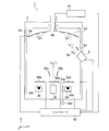
- the film forming apparatus 1 of the present embodiment includes a vertically placed cylindrical vacuum vessel 2.
- the vacuum vessel 2 is evacuated to a predetermined pressure by an evacuation unit (not shown).
- a load lock chamber may be connected to the vacuum vessel 2 through a door. When the load lock chamber is provided, the substrate 101 can be loaded and unloaded while the vacuum state in the vacuum vessel 2 is maintained.
- a stainless steel spherical substrate holder 4a ' is held above the inside of the vacuum vessel 2 so as to be rotatable about a vertical axis.
- An opening is provided in the center of the substrate holder 4a ', and a crystal monitor 50 is provided here.
- the crystal monitor 50 detects the physical film thickness by the film thickness detector 51 from the change in the resonance frequency due to the thin film adhering to the surface. The film thickness detection result is sent to the controller 52.
- An electric heater 53 is disposed inside the vacuum vessel 2 so as to enclose the substrate holder 4a '.
- the temperature of the substrate holder 4 a ′ is detected by a temperature sensor 54 such as a thermocouple, and the result is sent to the controller 52.
- the controller 52 appropriately controls the temperature of the substrate 101 by controlling the electric heater 53 using the output from the temperature sensor 54.
- evaporation sources 34 and 36 for attaching a film forming material to the substrate 101 held by the substrate holder 4a ′, and an ion gun 38 for irradiating the substrate 101 with positive ions. It is installed.
- the evaporation source 34 includes a crucible (boat) 34b provided with a depression for placing a film forming material thereon, an electron gun 34c that irradiates the film forming material with an electron beam (e ⁇ ), and a substrate from the crucible 34b. And a shutter 34a provided at a position where the film forming material toward 101 is blocked.
- a shutter 34a provided at a position where the film forming material toward 101 is blocked.
- the evaporation source 36 is a resistance heating type evaporation source such as a direct heating method or an indirect heating method.
- the evaporation source 36 includes a crucible (boat) 36b provided with a depression for placing a film forming material thereon, and a crucible 36b. And a shutter 36a that can be opened and closed at a position where the film forming material directed to the substrate 101 is blocked.
- a direct heating method an electrode is attached to a metal boat and an electric current is passed, and the metal boat is directly heated to use the boat itself as a resistance heater, and the film forming material placed therein is heated.
- the indirect heating method is a method in which a boat is not a direct heat source, but is heated by passing a current through a heating device provided separately from the boat, for example, a vapor deposition filament made of a rare metal such as a transition metal.
- a heating device provided separately from the boat, for example, a vapor deposition filament made of a rare metal such as a transition metal.
- the ion gun 38 is an ion assist ion source, and extracts charged ions (O 2 + , Ar + ) from a plasma of a reactive gas (such as O 2 ) or a rare gas (such as Ar), and a predetermined acceleration voltage. , And is emitted toward the substrate 101.
- a shutter 38a is disposed so as to be openable and closable.
- adjustment walls 38b and 38b for adjusting the directivity of ions extracted from the ion gun 38 are provided above the shutter 38a.
- the film forming material that moves from the evaporation sources 34 and 36 toward the substrate 101 adheres to the surface of the substrate 101 with high density and strength due to the collision energy of positive ions irradiated from the ion gun 38. At this time, the substrate 101 is positively charged by positive ions contained in the ion beam.
- positive ions for example, O 2 +
- ejected from the ion gun 38 accumulate on the substrate 101, thereby causing a phenomenon that the entire substrate 101 is positively charged (charge-up).
- charge-up occurs, abnormal discharge occurs between the positively charged substrate 101 and another member, and a thin film (insulating film) formed on the surface of the substrate 101 may be destroyed by an impact caused by the discharge.
- collision energy due to positive ions ejected from the ion gun 38 is reduced, so that the denseness and adhesion strength of the thin film may be reduced.
- the neutralizer 5 is disposed in the middle of the side wall of the vacuum vessel 2 for the purpose of electrically neutralizing (neutralizing) positive charges accumulated in the substrate 101.
- the neutralizer 5 emits electrons (e ⁇ ) toward the substrate 101 during irradiation of the ion beam by the ion gun 38.
- the neutralizer 5 extracts electrons from a plasma of a rare gas such as Ar and accelerates them with an acceleration voltage. To emit electrons.
- the electrons emitted from here neutralize charging by ions attached to the surface of the substrate 101.
- adjustment walls 5 a and 5 a for adjusting the directivity of electrons emitted from the neutralizer 5 are provided above the neutralizer 5.
- the first film 103 is formed by an ion beam assisted deposition method (IAD: Ion-beam Assisted Deposition method) using an ion gun, and ions are formed on the first film 103 by an ion gun.
- IAD Ion-beam Assisted Deposition method
- the form of the first film forming material is not particularly limited, and for example, a pellet-shaped material can be used.
- the heating of the first film-forming material is not limited to the electron beam heating method, and a heat source capable of sufficiently heating the vapor deposition material, such as a halogen lamp, a sheathed heater, resistance heating, induction heating, or the like, is used. Can do.
- the form of the second film forming material is not particularly limited.
- a porous ceramic impregnated with a hydrophobic reactive organic compound or
- a metal fiber or fine wire lump impregnated with a hydrophobic reactive organic compound They can quickly absorb and evaporate large amounts of hydrophobic reactive organic compounds.
- the porous ceramic is preferably used in the form of pellets from the viewpoint of handling properties.
- metal fibers or fine wires examples include iron, platinum, silver, and copper. It is preferable to use a metal fiber or a thin wire having a shape entangled so as to hold a sufficient amount of a hydrophobic reactive organic compound, for example, a woven fabric or a nonwoven fabric. The porosity of the metal fiber or fine wire lump can be determined depending on how much the hydrophobic reactive organic compound is retained.
- a lump of metal fibers or fine wires held in a container can be regarded as a pellet.
- the shape of the container is not particularly limited, and examples include a Knudsen type, a divergent nozzle type, a straight cylinder type, a divergent cylinder type, a boat type, and a filament type, and can be appropriately selected depending on the specifications of the vapor deposition apparatus. At least one end of the container is open, and the hydrophobic reactive organic compound evaporates from the open end.
- metals such as copper, tungsten, tantalum, molybdenum and nickel, ceramics such as alumina, carbon and the like can be used, and the material is appropriately selected depending on the vapor deposition apparatus and the hydrophobic reactive organic compound.
- the size of both the porous ceramic pellets and the pellets made of metal fibers or fine wire lumps held in a container is not limited.
- hydrophobic reactive organic compound When impregnating a porous ceramic or metal fiber or fine wire lump with a hydrophobic reactive organic compound, first prepare an organic solvent solution of the hydrophobic reactive organic compound, and then make the solution porous by dipping, dropping, spraying, etc. After impregnating the ceramic or metal fiber or fine wire, the organic solvent is volatilized. Since the hydrophobic reactive organic compound has a reactive group (hydrolyzable group), it is preferable to use an inert organic solvent.
- inert organic solvents examples include fluorine-modified aliphatic hydrocarbon solvents (perfluoroheptane, perfluorooctane, etc.), fluorine-modified aromatic hydrocarbon solvents (m-xylene hexafluoride, benzotrifluoride, etc.), fluorine Modified ether solvents (methyl perfluorobutyl ether, perfluoro (2-butyltetrahydrofuran), etc.), fluorine-modified alkylamine solvents (perfluorotributylamine, perfluorotripentylamine, etc.), hydrocarbon solvents (toluene, xylene, etc.) ), Ketone solvents (acetone, methyl ethyl ketone, methyl isobutyl ketone, etc.). These organic solvents may be used alone or in combination of two or more.
- the concentration of the hydrophobic reactive organic compound solution is not limited, and can be appropriately set according to the form of
- the heating of the second film-forming material is not limited to the resistance heating method, and a halogen lamp, a sheathed heater, an electron beam, a plasma electron beam, induction heating, or the like can also be used.
- a plurality of substrates 101 are fixed to the substrate holder 4a '.
- the substrate 101 fixed to the substrate holder 4a ' can be made of glass, plastic, or metal whose shape is processed into, for example, a plate shape or a lens shape. Note that the substrate 101 is preferably wet-cleaned before or after fixing.
- the inside of the vacuum vessel 2 is evacuated to about 10 ⁇ 4 to 10 ⁇ 2 Pa, for example.
- the degree of vacuum is lower than 10 ⁇ 4 Pa, it takes too much time for evacuation, and the productivity may be reduced.
- the degree of vacuum is higher than 10 ⁇ 2 Pa, film formation may be insufficient, and film characteristics may be deteriorated.
- the electric heater 53 is energized to generate heat, and the substrate holder 4a ′ is rotated at a low speed. By this rotation, the temperature and film forming conditions of the plurality of substrates 101 are made uniform.
- the controller 52 determines from the output of the temperature sensor 54 that the temperature of the substrate 101 has reached, for example, room temperature to 120 ° C., preferably 50 to 90 ° C., the controller 52 enters a film forming process.
- the substrate temperature is lower than room temperature, the density of the first film 103 to be formed is low, and there is a tendency that sufficient film durability cannot be obtained.
- the substrate temperature exceeds 120 ° C., when a plastic substrate is used as the substrate 101, the substrate 101 may be deteriorated or deformed.
- the film may be formed at room temperature.
- the ion gun 38 is set in an idle operation state before entering the film forming process.
- the evaporation sources 34 and 36 are also prepared so that the first film-forming material and the second film-forming material can be immediately diffused (released) by opening the shutters 34a and 36a.
- the controller 52 increases the irradiation power (power) of the ion gun 38 from the idle state to a predetermined irradiation power, opens the shutter 38a, opens the shutter 34a, and the ion beam of the first film-forming material.
- Assist vapor deposition (IAD) is performed.
- the operation of the neutralizer 5 is also started. That is, a step of scattering the first film-forming material from the evaporation source 34 on the film-forming surface of the substrate 101, a step of irradiating an ion beam of an introduction gas (here, oxygen) drawn from the ion gun 38, and electrons
- the irradiation step is performed in parallel (first film formation process).
- the ion beam assist conditions are as follows.
- the gas species introduced into the ion gun 38 for example, oxygen, argon, or a mixed gas of oxygen and argon is preferable.
- the amount of the gas species introduced into the ion gun 38 is, for example, 1 to 100 sccm, preferably 5 to 50 sccm.
- “Sccm” is an abbreviation for “standard cc / m”, and represents one at 0 ° C. and 101.3 kPa (1 atm).
- the acceleration voltage (V1) of ions is, for example, 100 to 2000V, preferably 200 to 1500V.
- the ion current density (I1) is, for example, 1 to 120 ⁇ A / cm 2 , preferably 5 to 50 ⁇ A / cm 2 .
- the ion irradiation time (T1) is, for example, 1 to 800 seconds, preferably 10 to 100 seconds.
- the ion beam may be irradiated in a range where the number of ions irradiated is, for example, 1 ⁇ 10 13 to 5 ⁇ 10 17 ions / cm 2 , preferably 5 ⁇ 10 13 to 5 ⁇ 10 14 ions / cm 2. it can.
- the irradiation time (T1) is shortened.
- the operating conditions of the neutralizer 5 are as follows.
- a gas species introduced into the neutralizer 5 for example, argon is used.
- the amount of the gas species introduced is, for example, 10 to 100 sccm, preferably 30 to 50 sccm.
- the acceleration voltage of electrons is, for example, 20 to 80V, preferably 30 to 70V.
- the electron current may be a current that can supply a current higher than the ion current.
- three-dimensional nuclei are formed on the substrate 101 in the initial stage of film formation, and then they grow and coalesce as the film formation amount (deposition amount) increases. Grows into a continuous film (island growth).
- the first film 103 made of SiO 2 is formed on the surface of the substrate 101 with a predetermined thickness.
- the controller 52 continues to monitor the film thickness of the thin film formed on the substrate 101 with the crystal monitor 50, and stops the film formation when a predetermined film thickness is reached.
- the controller 52 closes only the shutter 34a and keeps the shutter 38a open. In this state, the controller 52 changes the irradiation power of the ion gun 38 to a predetermined irradiation power and continues the ion beam irradiation.
- This step is an example of a first irradiation process (post irradiation). This embodiment is characterized in that post-irradiation is performed on the first film 103 formed on the surface of the substrate 101.
- the surface portion of the first film 103 is scraped off, and as a result, an appropriate recess is provided on the surface of the first film 103.
- the post-irradiation conditions are as follows.
- the gas species introduced into the ion gun 38 only needs to contain at least argon or oxygen, and may be a mixed gas of argon and oxygen, but preferably contains at least argon.
- the introduction amount of the above gas species is, for example, 10 to 100 sccm, preferably 20 to 70 sccm.
- the acceleration voltage (V2) of ions is, for example, 100 to 2000V, preferably 200 to 1500V.
- the ion current density (I2) is, for example, 1 to 120 ⁇ A / cm 2 , preferably 5 to 50 ⁇ A / cm 2 .
- the ion irradiation time (T2) is, for example, 1 to 800 seconds, preferably 10 to 100 seconds.
- the number is, for example, 1 ⁇ 10 13 to 5 ⁇ 10 17 pieces / cm 2 , preferably 1 ⁇ 10 13 to 1 ⁇ 10 17 pieces / cm 2 , more preferably 1 ⁇ 10 14 to 1 ⁇ 10 16 pieces / cm 2.
- the ion beam can be irradiated within the range.
- the irradiation time (T2) is shortened.
- the controller 52 returns the irradiation power of the ion gun 38 to the idle state, closes the shutter 38a, opens the shutter 36a, and resistance-heats the second film-forming material as an oil-repellent film forming raw material. Vacuum deposition is performed. That is, the second film-forming material is scattered from the evaporation source 36 to the post-irradiation surface of the first film 103 for 3 to 20 minutes, for example, and a film-forming process is performed (second film-forming process).
- the oil-repellent film 105 is formed with a predetermined thickness (for example, 1 to 50 nm) on the first film 103 after the post-irradiation.
- the controller 52 continues to monitor the film thickness of the thin film formed on the first film 103 with the crystal monitor 50, and stops vapor deposition when the film thickness reaches a predetermined value.
- the oil-repellent substrate 100 shown in FIG. 1 is manufactured.
- the first film 103 formed on the surface of the substrate 101 prior to the film formation of the oil repellent film 105 is used.
- the ion beam of the introduced gas is irradiated (post irradiation). For this reason, an appropriate recess is formed on the surface of the first film 103 after the ion beam irradiation. Accordingly, the oil-repellent molecules that are subsequently formed and are constituents of the oil-repellent film 105 can be attached to the recesses of the first film 103.
- oil such as fingerprints attached to the surface of the oil-repellent film 105 was wiped off with a heavy load (for example, a load of about 1 kg / cm 2 ).
- a heavy load for example, a load of about 1 kg / cm 2 .
- the constituent components of the oil-repellent film 105 can be effectively left on the outermost surface. That is, according to the present embodiment, it is possible to form the oil-repellent film 105 having wear resistance that can withstand practical use.
- the case where only the SiO 2 thin film is formed as the first film 103 on the substrate 101 is illustrated, but together with this SiO 2 thin film, for example, a Si 3 N 4 thin film or a ZrO 2 thin film is formed. It is also possible to stack other thin films. Further, as the first film 103 formed on the substrate 101, another thin film such as a Si 3 N 4 thin film or a ZrO 2 thin film may be formed instead of the SiO 2 thin film. In any case, in these cases, the material and form of the first film forming material filled in the vapor deposition source 34 may be changed as appropriate. In the present embodiment, the surface treatment of the substrate 101 can be performed prior to the first film formation process.
- the controller 52 increases the irradiation power (power) of the ion gun 38 from the idle state to a predetermined irradiation power.
- the shutter 38a is opened, and the surface of the substrate 101 before the first film formation process in the middle of rotation may be irradiated with an ion beam.
- the pre-irradiation conditions may be the same as the post-irradiation described above, but may be different conditions.
- the pre-irradiation conditions are as follows.
- the gas species introduced into the ion gun 38 only needs to contain at least argon or oxygen, and may be a mixed gas of argon and oxygen, but is preferably a mixed gas of argon and oxygen.
- the introduction amount of the above gas species is, for example, 10 to 100 sccm, preferably 20 to 70 sccm.
- the acceleration voltage (V3) of ions is, for example, 100 to 2000V, preferably 200 to 1500V.
- the ion current density (I3) is, for example, 1 to 120 ⁇ A / cm 2 , preferably 5 to 50 ⁇ A / cm 2 .
- the ion irradiation time (T3) is, for example, 60 to 1200 seconds, preferably 120 to 900 seconds, and more preferably 180 to 720 seconds.
- the number of irradiated ions is, for example, 5 ⁇ 10 14 to 5 ⁇ 10 17 ions / cm 2 , preferably 1 ⁇ 10 15 to 1 ⁇ 10 17 ions / cm 2 , more preferably 1 ⁇ 10 16 to 1 It is preferable to irradiate the ion beam in a range of ⁇ 10 17 / cm 2 .
- the irradiation time (T3) is shortened.
- the surface of the first film 103 may have irregularities before the post-irradiation (5).
- the post-irradiation (5) the concave portion already included in the first film 103 may be scraped off first, and the substrate 101 may be exposed.
- This embodiment includes an aspect in which a part of the substrate 101 is exposed by post-irradiation.
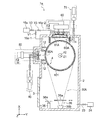
- the film forming apparatus 1 a includes a vacuum vessel 2.
- a rotary drum 4 is held above the inside of the vacuum vessel 2 so as to be rotatable around an axis orthogonal to the vertical axis. Yes.
- the rotating drum 4 as a substrate holding mechanism is a cylindrical member for holding the substrate 101 as a film formation target inside the vacuum vessel 2.
- the rotating drum 4 includes a plurality of substrate holders 4a, a frame 4b, and a fastener 4c that fastens the substrate holder 4a and the frame 4b.
- the substrate holder 4a is provided with a plurality of substrate holding holes for holding the substrate 101 in a row in the center of the plate surface along the longitudinal direction of the substrate holder 4a.
- the substrate 101 is accommodated in the substrate holding hole of the substrate holder 4a, and is fixed to the substrate holder 4a using a screw member or the like so as not to drop off.
- the screw hole which can insert the fastener 4c is provided in the plate surface in the both ends of the longitudinal direction (Z direction) of the board
- the frame 4b is composed of two annular members arranged vertically (X direction). Each annular member is provided with a screw hole at a position corresponding to the screw hole of the substrate holder 4a.
- the substrate holder 4a and the frame 4b are fixed using a fastener 4c made of, for example, a bolt and a nut.
- the rotating drum 4 is configured to be movable between the inside of the vacuum vessel 2 and a load lock chamber connected to the vacuum vessel 2 through a door.
- the rotary drum 4 is disposed inside the vacuum vessel 2 such that the central axis Z1 in the cylindrical direction (Z direction) of the cylinder is in the front-rear direction (Z direction) of the vacuum vessel 2.
- the rotating drum 4 is transported to the load lock chamber when the substrate holder 4a is attached to or removed from the frame 4b, and the substrate holder 4a is attached to or detached from the frame 4b in the load lock chamber. On the other hand, the rotating drum 4 is transported into the vacuum container 2 during film formation and is allowed to rotate within the vacuum container 2.
- the central portion of the rear surface of the rotating drum 4 is configured to engage with the front surface of the motor rotating shaft 40a.
- the rotating drum 4 and the motor rotating shaft 40a are positioned so that the center axis of the motor rotating shaft 40a and the center axis Z1 of the rotating drum 4 coincide with each other, and are connected by engaging both.
- the surface of the rear surface of the rotating drum 4 that engages with the motor rotating shaft 40a is made of an insulating member. Thereby, abnormal discharge of the substrate 101 can be prevented. In addition, an air-tightness is maintained between the vacuum vessel 2 and the motor rotating shaft 40a by an O-ring.
- the motor rotating shaft 40a is rotated by driving the motor 40 provided at the rear part of the vacuum vessel 2 while maintaining the vacuum state inside the vacuum vessel 2. Along with this rotation, the rotating drum 4 connected to the motor rotating shaft 40a rotates around the axis Z1. Since each board
- a drum rotating shaft 42 is provided on the front surface of the rotating drum 4, and the drum rotating shaft 42 rotates as the rotating drum 4 rotates.
- a hole is formed in the front wall surface (Z direction) of the vacuum vessel 2, and the drum rotation shaft 42 passes through this hole and communicates with the outside of the vacuum vessel 2.
- a bearing is provided on the inner surface of the hole so that the rotating drum 4 can be smoothly rotated.
- the vacuum vessel 2 and the drum rotation shaft 42 are kept airtight with an O-ring.
- the partition wall 12 is erected at a position facing the rotary drum 4 for measuring the vacuum vessel 2 in the vertical direction (X direction).
- the partition wall 12 is the same stainless steel member as the vacuum vessel 2.
- the partition wall 12 is composed of flat plate members arranged one by one on the top, bottom, left, and right, and is in a state of enclosing four sides from the inner wall surface of the vacuum vessel 2 toward the rotary drum 4. Thereby, the sputter region 80A is partitioned inside the vacuum vessel 2.
- the side wall of the vacuum vessel 2 has a convex cross section projecting outward, and a sputter means 80 is provided on the projecting wall surface.
- the sputter region 80 ⁇ / b> A is formed in a region surrounded by the inner wall surface of the vacuum vessel 2, the partition wall 12, the outer peripheral surface of the rotating drum 4, and the sputter means 80.
- a sputtering process is performed in which a film raw material is attached to the surface of the substrate 101.
- the sputtering means 80 includes a pair of targets 82a and 82b, a pair of sputtering electrodes 81a and 81b that hold the targets 82a and 82b, and an AC power source 84 that supplies power to the sputtering electrodes 81a and 81b. , And a transformer 83 as power control means for adjusting the amount of power from the AC power supply 84.
- the wall surface of the vacuum vessel 2 protrudes outward, and the sputter electrodes 81a and 81b are disposed on the inner wall of the protruding portion so as to penetrate the side wall.
- the sputter electrodes 81a and 81b are fixed to the vacuum vessel 2 at the ground potential via an insulating member.
- the targets 82a and 82b are formed by forming the first film forming material into a flat plate shape, and are held by the sputtering electrodes 81a and 81b so as to face the side surfaces of the rotating drum 4 as described later.
- a material having a hardness higher than the hardness of the substrate 101 for example, metal silicon (Si), aluminum (Al), zirconium (Zr), or the like, by oxidizing, nitriding, or oxynitriding. Is used.
- Si target silicon
- the sputter electrodes 81a and 81b have a structure in which a plurality of magnets are arranged in a predetermined direction.
- the sputter electrodes 81a and 81b are connected to an AC power source 84 via a transformer 83, and are configured so that an alternating electric field of 1 to 100 kHz can be applied to both electrodes.
- Targets 82a and 82b are held on the sputter electrodes 81a and 81b, respectively.
- the shapes of the targets 82a and 82b are flat, and are installed so that the longitudinal direction of the targets 82a and 82b is parallel to the rotation axis Z1 of the rotary drum 4 as shown in FIG.
- a sputtering gas supply means 90 for supplying a sputtering gas such as argon is provided around the sputtering region 80A.
- the sputter gas supply means 90 includes a sputter gas cylinder 92 as a sputter gas storage means, pipes 95a and 95c as sputter gas supply paths, and a mass flow controller 91 as a sputter gas flow rate adjusting means for adjusting the flow rate of the sputter gas. I have.
- sputtering gas examples include inert gases such as argon and helium.
- the sputter gas cylinder 92 and the mass flow controller 91 are both provided outside the vacuum vessel 2.
- the mass flow controller 91 is connected to a single sputtering gas cylinder 92 that stores the sputtering gas via a pipe 95c.
- the mass flow controller 91 is connected to the pipe 95a, and one end of the pipe 95a passes through the side wall of the vacuum vessel 2 and extends in the vicinity of the targets 82a and 82b in the sputtering region 80A.
- the front end of the pipe 95a is disposed near the lower center of the targets 82a and 82b, and an introduction port 95b opens toward the front center of the targets 82a and 82b.
- the mass flow controller 91 is a device that adjusts the gas flow rate.
- the mass flow controller 91 is an inflow port through which the gas from the sputter gas cylinder 92 flows in, an outflow port through which the sputter gas flows out into the pipe 95a, a sensor that detects the mass flow rate of the gas, A control valve for adjusting the gas flow rate, a sensor for detecting the mass flow rate of the gas flowing in from the inlet, and an electronic circuit for controlling the control valve based on the flow rate detected by the sensor are provided.
- a desired flow rate can be set from the outside.
- the sputter gas from the sputter gas cylinder 92 is introduced into the pipe 95 a with the flow rate adjusted by the mass flow controller 91.
- the sputtering gas that has flowed into the pipe 95a is introduced from the introduction port 95b to the front surfaces of the targets 82a and 82b disposed in the sputtering region 80A.
- Sputtering gas is supplied from the sputtering gas supply means 90 to the sputtering region 80A, and an alternating electrode is applied from the AC power source 84 to the sputtering electrodes 81a and 81b in a state where the surroundings of the targets 82a and 82b are in an inert gas atmosphere. Then, part of the sputtering gas around the targets 82a and 82b emits electrons and is ionized. A leakage magnetic field is formed on the surfaces of the targets 82a and 82b by the magnets arranged on the sputter electrodes 81a and 81b.
- these electrons circulate in a magnetic field generated near the surfaces of the targets 82a and 82b while drawing a toroidal curve.
- a strong plasma is generated along the trajectory of the electrons, and ions of the sputtering gas are accelerated toward the plasma and collide with the targets 82a and 82b, whereby atoms and particles on the surfaces of the targets 82a and 82b (targets 82a and 82b).
- Si Si
- Si atoms and Si particles are knocked out.
- the knocked-out Si atoms and Si particles adhere to the surface of the substrate 101 to form an ultrathin film.
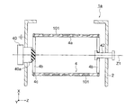
- a partition wall 14 is erected on the upper inner wall arranged in the vertical direction (X direction) of the vacuum vessel 2 at a position facing the rotary drum 4.
- the partition wall 14 is made of, for example, stainless steel that is the same component as the vacuum vessel 2.
- the partition wall 14 is composed of flat plate members arranged one by one on the top, bottom, left, and right, and is in a state of enclosing four sides from the upper inner wall surface of the vacuum vessel 2 toward the rotary drum 4. Thereby, the plasma processing region 60 ⁇ / b> A is partitioned inside the vacuum container 2.
- the rotation drum 4 is sandwiched between the vapor deposition region 30A and the opposite direction (upward in the vertical direction of the vacuum chamber 2; approximately 180 ° direction), and the sputter region 80A is approximately 90.
- a plasma processing region 60A is provided at a position spatially separated from both the vapor deposition processing region 30A and the sputtering region 80A.
- the upper inner wall of the vacuum vessel 2 has a convex cross section projecting outward (upward), and the projecting wall surface is provided with a plasma generating means 60 so as to face the plasma processing region 60A.
- the plasma processing region 60A is formed in a region surrounded by the inner wall surface of the vacuum vessel 2, the partition wall 14, the outer peripheral surface of the rotary drum 4, and the plasma generating means 60.
- the surface of the substrate 101 is formed in the sputtering region 80A.
- the ultrathin film attached to the substrate is subjected to a reaction treatment to form a thin film made of a Si compound or an incomplete compound.
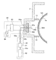
- an opening 2a for installing the plasma generating means 60 is formed on the upper wall surface of the vacuum vessel 2 corresponding to the plasma processing region 60A.
- a pipe 75a is connected to the plasma processing region 60A.
- a mass flow controller 72 is connected to one end of the pipe 75 a, and this mass flow controller 72 is further connected to a reactive gas cylinder 71. For this reason, the reactive gas can be supplied from the reactive gas cylinder 71 into the plasma processing region 60A.
- the plasma generating means 60 includes a case body 61, a dielectric plate 62, an antenna 63, a matching box 64, and a high frequency power supply 65.
- the case body 61 has a shape for closing the opening 2a formed on the wall surface of the vacuum vessel 2, and is fixed so as to close the opening 2a of the vacuum vessel 2 with a bolt.
- the plasma generating means 60 is attached to the wall surface of the vacuum vessel 2 by fixing the case body 61 to the wall surface of the vacuum vessel 2.
- Case body 61 is formed of stainless steel.
- the dielectric plate 62 is formed of a plate-like dielectric.
- the dielectric plate 62 is made of quartz, but the material of the dielectric plate 62 is not limited to such quartz, but may be made of a ceramic material such as Al 2 O 3 .
- the dielectric plate 62 is fixed to the case body 61 with a fixed frame. When the dielectric plate 62 is fixed to the case body 61, the antenna accommodating chamber 61 ⁇ / b> A is formed in a region surrounded by the case body 61 and the dielectric plate 62.
- the dielectric plate 62 fixed to the case body 61 is provided facing the inside of the vacuum vessel 2 (plasma processing region 60A) through the opening 2a.
- the antenna accommodating chamber 61A is separated from the inside of the vacuum vessel 2. That is, the antenna accommodating chamber 61 ⁇ / b> A and the inside of the vacuum container 2 form an independent space in a state where the antenna accommodating chamber 61 ⁇ / b> A is partitioned by the dielectric plate 62. Further, the antenna accommodating chamber 61 ⁇ / b> A and the outside of the vacuum vessel 2 form an independent space in a state of being partitioned by the case body 61.
- the antenna 63 is installed in the antenna accommodating chamber 61A formed as an independent space in this way. In addition, airtightness is maintained by the O-ring between the antenna housing chamber 61A and the inside of the vacuum vessel 2 and between the antenna housing chamber 61A and the outside of the vacuum vessel 2, respectively.
- the pipe 16a-2 branches from the pipe 16a-1.
- the pipe 16a-2 is connected to the antenna accommodating chamber 61A, and has a role as an exhaust pipe when the inside of the antenna accommodating chamber 61A is evacuated to be in a vacuum state.
- valves V1 and V2 are provided at positions where the vacuum pump 15a communicates with the inside of the vacuum vessel 2. Further, the pipe 16a-2 is provided with a valve V3 at a position where it communicates from the vacuum pump 15a to the inside of the antenna accommodating chamber 61A. By closing either one of the valves V2 and V3, gas movement between the inside of the antenna accommodating chamber 61A and the inside of the vacuum vessel 2 is prevented. The pressure inside the vacuum chamber 2 and the pressure inside the antenna housing chamber 61A are measured with a vacuum gauge.
- the film forming apparatus 1a (see FIG. 3) of this embodiment is provided with a control device.
- the output of the vacuum gauge is input to this control device.
- the control device has a function of adjusting the degree of vacuum inside the vacuum vessel 2 and inside the antenna accommodating chamber 61A by controlling the exhaust by the vacuum pump 15a based on the input measurement value of the vacuum gauge.
- the control device controls the opening and closing of the valves V1, V2, and V3, so that the inside of the vacuum container 2 and the inside of the antenna housing chamber 61A can be exhausted simultaneously or independently.
- the film formation atmosphere in the sputtering region 80A can be stabilized by appropriately controlling the vacuum pump 15a.
- the antenna 63 is a means for receiving an electric power from the high frequency power supply 65 to generate an induction electric field inside the vacuum vessel 2 (plasma processing region 60A) and to generate plasma in the plasma processing region 60A.
- the antenna 63 includes a tubular main body portion made of copper and a covering layer made of silver covering the surface of the main body portion. That is, the main body of the antenna 63 is formed into a circular tube shape with copper that is inexpensive and easy to process and has low electrical resistance, and the surface of the antenna 63 is covered with silver having a lower electrical resistance than copper. Thereby, the impedance of the antenna 63 with respect to a high frequency is reduced, and the efficiency of generating plasma is increased by flowing a current through the antenna 63 efficiently.
- the film forming apparatus 1a (see FIG. 3) of the present embodiment is configured to generate a reactive gas plasma in the plasma processing region 60A by applying an AC voltage of 1 to 27 MHz to the antenna 63 from the high frequency power supply 65. Has been.
- the antenna 63 is connected to a high frequency power source 65 through a matching box 64 that accommodates a matching circuit.
- a variable capacitor (not shown) is provided in the matching box 64.
- the antenna 63 is connected to the matching box 64 through a conductor portion.
- the conductor portion is made of the same material as that of the antenna 63.
- the case body 61 is formed with an insertion hole for inserting the conducting wire portion, and the antenna 63 inside the antenna accommodating chamber 61A and the matching box 64 outside the antenna accommodating chamber 61A are led through the inserting hole. Connected through the unit.
- a seal member is provided between the conductor portion and the insertion hole, and airtightness is maintained inside and outside the antenna accommodating chamber 61A.
- a grid 66 may be provided as an ion extinguishing means.
- the grid 66 is for extinguishing part of ions and part of electrons generated by the antenna 63.
- the grid 66 is a hollow member made of a conductor and is grounded.
- a cooling medium for example, cooling water
- a hose for supplying the cooling medium is connected to an end of the grid 66.
- reactive gas supply means 70 is provided in and around the plasma processing region 60A.
- the reactive gas supply means 70 of this embodiment includes a reactive gas cylinder 71 that stores a reactive gas (for example, oxygen gas, nitrogen gas, fluorine gas, ozone gas, etc.) and a reactive gas cylinder 71 that supplies the reactive gas.
- a mass flow controller 72 for adjusting the flow rate and a pipe 75a for introducing a reactive gas into the plasma processing region 60A are provided.
- the substrate 101 held on the outer peripheral surface of the rotating drum 4 is revolved, and a position facing the sputtering region 80A and a position facing the plasma processing region 60A. It will move repeatedly between.
- the substrate 101 revolves in this manner the sputtering process in the sputtering region 80A and the plasma process in the plasma processing region 60A are sequentially repeated, and a thin film (first film 103) is formed on the surface of the substrate 101. ) Is formed.
- the antenna 63 faces the antenna 63 in the plasma processing region 60A. Plasma is generated in the region, and the first film formation material formed on the surface of the substrate 101 is densified to form a thin film (first film 103) having sufficient characteristics.
- an evaporation treatment region 30 ⁇ / b> A is provided below the vacuum container 2 in the vertical direction (X direction).
- the vapor deposition region 30A is a region where the oil repellent film 105 is formed on the surface of the first film 103 formed on the surface of the substrate 101 by a vapor deposition method.
- a resistance heating type vapor deposition source 36 is provided below the vapor deposition region 30A (inner bottom wall of the vacuum chamber 2). Since the configuration of the evaporation source 36 is the same as that of the second embodiment, the description thereof is omitted.
- An exhaust pipe 23 is connected to the inner bottom wall of the vacuum vessel 2, and a vacuum pump 24 for exhausting the vicinity of the vapor deposition source 36 is connected to the pipe 23.
- the degree of vacuum in the vacuum vessel 2 can be adjusted by a vacuum pump 24 and a controller (not shown).
- the door 3 is provided in the measurement (Z direction) of the vacuum vessel 2, and the door 3 is opened and closed by sliding or rotating.
- a load lock chamber may be connected to the outside of the door 3 separately.
- an ion gun 38 is further disposed below the vacuum vessel 2 in the vertical direction (X direction). Since the configuration of the ion gun 38 is the same as that of the second embodiment, the description thereof is omitted.
- metal silicon (Si) as the first film forming material is used as the targets 82a and 82b, and the second film forming material as the raw material for forming the oil repellent film is put into the boat of the evaporation source 36. To do. Moreover, the case where nitrogen gas is used as reactive gas is illustrated.
- the first film 103 is formed by the sputtering method, the first film 103 is subjected to a first irradiation process (post-irradiation) by an ion beam using an ion gun.
- a first irradiation process post-irradiation
- An example in which the oil-repellent film 105 is formed by a vacuum deposition method is illustrated.
- the first film 103 is formed by sputtering, for example, a sputtering process in which a thin film that is considerably thinner than a target film thickness is attached to the surface of the substrate 101, and a nitriding treatment is performed on the thin film to form a thin film.
- the intermediate thin film is formed on the surface of the substrate 101 by the reaction process for converting the composition of the substrate, and the sputtering process and the reaction process are repeated a plurality of times, so that a plurality of intermediate thin films are stacked to form a final thin film having a desired film thickness.
- the first film 103 is formed on the surface of the substrate 101.
- a first film 103 is formed as a final thin film having a thickness of about nm to several hundred nm.
- the substrate 101 was set on the rotary drum 4 outside the vacuum vessel 2 and accommodated in the load lock chamber of the vacuum vessel 2.
- the substrate 101 is preferably wet-cleaned before or after setting.
- the rotary drum 4 is moved into the vacuum vessel 2 along the rail.
- the targets 82a and 82b in the sputter region 80A are held by the sputter electrodes 81a and 81b.
- the inside of the vacuum vessel 2 is sealed, and the inside of the vacuum vessel 2 is depressurized to a predetermined pressure using the vacuum pump 15a.
- the rotational speed (RS) of the rotating drum 4 is selected, for example, at 25 rpm or higher, preferably 30 rpm or higher, more preferably 50 rpm or higher. If the value of RS is made too small, the sputtering time for one substrate 101 becomes long. As a result, the film thickness of the thin film formed on the substrate 101 becomes thick, and the plasma processing in the plasma processing region 60A is sufficiently performed. There is a tendency that can not be done.
- the upper limit of RS is preferably 250 rpm, more preferably 200 rpm, and even more preferably 100 rpm.
- the substrate 101 may be heated at a low temperature of about 220 ° C. or lower, preferably 150 ° C. or lower, more preferably 100 ° C. or lower, more preferably 80 ° C. or lower, and preferably about 50 ° C. or higher. Good.
- the time for this process is set to an appropriate time within a range of about 1 to 60 minutes, for example.
- the flow rate of the nitrogen gas is appropriately determined within a range of about 70 to 500 sccm and the power supplied from the high frequency power supply 65 within a range of 1.0 to 5.0 kW.
- the pressure (deposition pressure) of nitrogen gas introduced into the plasma processing region 60A is preferably about 0.3 to 0.6 Pa.
- the flow rate of nitrogen gas can be adjusted by the mass flow controller 72, and the power supplied from the high frequency power supply 65 can be adjusted by the matching box 64.
- the rotating drum 4 is continuously rotated, and a plurality of intermediate thin films are stacked by sequentially repeating the sputtering process and the plasma process, and the first film 103 made of a Si 3 N 4 thin film having a desired thickness. (First film formation process).
- this pretreatment may be a short time of about 1 to 10 minutes, for example.
- the irradiation power (power) of the ion gun 38 is increased from the idle state to a predetermined irradiation power, the shutter 38a is opened, and the first Irradiation of the ion beam to the film 13 is started.
- This step is an example of a first irradiation process (post irradiation).
- This embodiment is also characterized in that post-irradiation is performed on the first film 103 formed on the surface of the substrate 101. Post-irradiation can be performed under the same conditions as in the second embodiment.
- the irradiation power of the ion gun 38 is returned to the idle state, the shutter 38a is closed, the shutter 36a is opened, and the vapor deposition process region 30A is operated.
- the second film-forming material as a raw material for forming the oil-repellent film filled in the crucible (boat) 36b is heated.
- the inside of the vacuum vessel 2 is sealed, and the inside of the vacuum vessel 2 is depressurized to a predetermined pressure using the vacuum pump 15a.
- the heated second film-forming material diffuses into the vapor deposition process region 30A, and a part of the second film-forming material after the post-irradiation of the substrate 101 held by the rotating drum 4 is rotated.
- a film having a predetermined thickness is formed on the surface of the first film 103 (second film formation process).
- the film formation rate of the second film formation material is, for example, 0.1 nm / second or more, preferably 0.2 to 0.4 nm / second.
- the oil-repellent film 105 is formed with a predetermined thickness on the first film 103 after the post-irradiation.
- the oil-repellent substrate 100 shown in FIG. 1 is manufactured.
- the case where only the Si 3 N 4 thin film is formed as the first film 103 on the substrate 101 is illustrated.
- a SiO 2 thin film or an Al 2 film is used.
- Other thin films such as an O 3 thin film can be laminated.
- region 80A is just to change suitably the material of the targets 82a and 82b of the sputtering means 80 installed in the sputtering area
- the first film 103 formed on the substrate 101 another thin film such as a SiO 2 thin film or an Al 2 O 3 thin film may be formed instead of the Si 3 N 4 thin film.
- the material of the targets 82a and 82b is appropriately changed to various metals such as Al, Zr and Cr or a plurality of types of metals, or the reactive gas is changed to oxygen gas, fluorine gas, ozone gas or the like, for example. Good.
- the substrate 101 prior to the first film formation process, the substrate 101 may be subjected to a second irradiation process (pre-irradiation) similar to the second embodiment.
- the pre-irradiation includes the plasma treatment (4).
- the case where the ion gun 38 is disposed below the vacuum vessel 2 in the vertical direction is exemplified, but the ion gun 38 is not necessarily installed.
- a bias voltage is applied to the rotating drum 4
- directivity is imparted to ions in the thermal plasma of the plasma generating means 60 by the bias voltage.
- ions imparted with directivity collide with the surface of the first film 103 formed in (3) and (4) described above under appropriate conditions, appropriate unevenness is imparted to the first film 103.
- Example 1 In this example, a film forming apparatus 1 shown in FIG. 2 configured to perform ion beam assisted vapor deposition was prepared, and film formation was performed under the conditions shown in Table 1 to obtain an oil-repellent substrate sample.
- the substrate 101 a glass substrate having a pencil hardness of 6H was used.
- the “hardness” here is a value of pencil hardness measured by a method according to JIS-K5600-5-4.
- the substrate 101 was wet cleaned before film formation.
- the surface of the substrate 101 is subjected to ion beam-assisted deposition (first film-forming process) of the first film-forming material.
- the ion cleaning conditions were acceleration voltage: 1000 V, current: 30 ⁇ A / cm 2 , introduced gas type and introduced amount: (30 sccm O 2 +20 sccm Ar).
- the substrate temperature during the first film formation process was 150 ° C.
- the operating conditions of the neutralizer excluding Experimental Example 2 were acceleration voltage: 30 to 70 V, electron current: 1 A, introduced gas type: (O 2 + Ar), and introduced amount of the gas: 50 sccm.
- the hardness of the SiO 2 thin film before and after the first irradiation treatment (post-irradiation) is a pencil hardness value measured by the above method.
- the “center line average roughness (Ra)”, “ten-point average height (Rz)” and “maximum valley depth (Pv)” of the SiO 2 thin film after post-irradiation were measured according to JIS-B0601. Value.
- the “convex period” of the SiO 2 thin film after post-irradiation is a value measured with an atomic force microscope (AFM) (trade name “SPI-3700” manufactured by Seiko Denshi Kogyo Co., Ltd.).
- AFM atomic force microscope
- As the second film forming material an oil repellent (trade name: OF-SR, component name: fluorine-containing organosilicon compound) manufactured by Canon Optron, Inc. was used.
- Example 2 the film forming apparatus 1a shown in FIG. 3 to FIG. 6 configured to perform magnetron sputtering was prepared, and film formation was performed under the conditions shown in Table 2 to obtain an oil-repellent substrate sample.
- the substrate 101 a glass substrate having a pencil hardness of 6H was used.
- the “hardness” here is a value of pencil hardness measured by a method according to JIS-K5600-5-4.
- the substrate 101 was wet cleaned before film formation.
- the targets 82a and 82b a flat plate and a metal silicon (Si) target were used, and the surface of the substrate 101 was pretreated by plasma treatment for 1 minute prior to the first film formation treatment.
- the rotational speed (RS) of the rotating drum 4 was 100 rpm.
- the substrate temperature during the first film formation process was 100 ° C.
- the hardness of the Si 3 N 4 thin film before and after the first irradiation treatment (post irradiation) is a pencil hardness value measured by the above method when converted to a thickness of 100 nm.
- the Ra, Rz, and Pv of the Si 3 N 4 thin film after post-irradiation are values measured in accordance with JIS-B0601.
- the “convex period” of the Si 3 N 4 thin film after post-irradiation is a value measured by an atomic force microscope (AFM) (trade name “SPI-3700” manufactured by Seiko Denshi Kogyo Co., Ltd.).
- AFM atomic force microscope
- As the second film forming material an oil repellent (trade name: OF-SR, component name: fluorine-containing organosilicon compound) manufactured by Canon Optron, Inc. was used.
- the scratch resistance is ensured by the convex portions, and the components of the oil-repellent film 105 remain here by the concave portions, thereby ensuring the oil repellency of the sample surface, It is considered that wear resistance that can withstand practical use has been imparted.
Abstract
Description
第1の成膜工程をイオンアシスト蒸着法で行う場合、これに用いるイオンビームとしては、例えば加速電圧が100~2000Vのイオンビーム、電流密度が1~120μA/cm2 のイオンビーム、又は加速電圧が100~2000Vで電流密度が1~120μA/cm2 のイオンビームを用いることができる。第1の成膜工程において、イオンビームの照射時間は例えば1~800秒とすることができ、またイオンビームの粒子照射数は例えば1×10¹³個/cm2 ~5×10¹⁷個/cm2 とすることができる。第1の成膜工程に用いられるイオンビームは、酸素のイオンビーム、アルゴンのイオンビーム、又は酸素とアルゴンの混合ガスのイオンビームとすることができる。
《第1実施形態》
本実施形態では、撥油性基材の一例を説明する。
本実施形態では、図1の撥油性基材100を製造可能な成膜装置の一例を説明する。
図2に示すように、本実施形態の成膜装置1は、縦置き円筒状の真空容器2を含む。真空容器2は、排気手段(図示省略)によって所定の圧力に排気されるようになっている。真空容器2には、扉を介して、ロードロック室が接続されていてもよい。ロードロック室を備えていると、真空容器2内の真空状態を保持した状態で、基板101の搬入出を行うことが可能となる。
本実施形態では、蒸発源34のボートに充填する第1成膜材料として金属ケイ素(Si)または酸化ケイ素(SiO2 )を用いる場合を例示する。蒸発源36のボートに充填する撥油性膜の形成原料としての第2成膜材料については特に限定しない。
多孔質セラミックに疎水性反応性有機化合物を含浸させたものや、(b) 金属繊維又は細線の塊に疎水性反応性有機化合物を含浸させたものを用いることができる。これらは、多量の疎水性反応性有機化合物を素早く吸収し、蒸発させることができる。多孔質セラミックは、ハンドリング性の観点からペレット状で用いることが好ましい。
コントローラ52は、基板101の温度が、例えば常温~120℃、好ましくは50~90℃になったことを温度センサ54の出力により判定すると、成膜工程に入る。基板温度が常温未満では成膜される第1の膜103の密度が低く、十分な膜耐久性が得られない傾向がある。基板温度が120℃を超えると基板101としてプラスチック基板を用いている場合に、その基板101の劣化や変形が起きる可能性がある。なお、無加熱成膜が好適な材料を用いる場合には常温で成膜することもある。
なお、例えば照射電力密度を大きくする場合には照射時間(T2)を短くし、反対に照射電力密度を小さくする場合には照射時間(T2)を長くすることによって、照射エネルギー密度(=V2×I2×T2)を制御することもできる。
また、本実施形態では、第1の成膜処理に先立ち、基板101の表面処理を行うこともできる。具体的には、1)酸素又はアルゴン雰囲気下におけるプラズマ処理、2)酸・アルカリによる薬品処理、3)イオン銃38によるエネルギーを持つ粒子の照射処理(第2の照射処理。前照射)、などを挙げることができる。これらのうちで、第2の照射処理(前照射)が望ましい。第1の成膜処理に先立って基板101に対し第2の照射処理(前照射)を行う場合、コントローラ52は、イオン銃38の照射電力(パワー)をアイドル状態から所定の照射電力に増大させ、シャッタ38aを開き、回転途中の、第1の成膜処理前の基板101の表面にイオンビームを照射すればよい。基板101に成膜される第1の膜103への後照射を行う前に、基板101に対し前照射を行うことで、第1の膜103の表面に、より適切な凹部を付与することができる。
前照射の条件は、上述した後照射と同一条件であってもよいが、異なる条件とすることもできる。
本実施形態では、図1の撥油性基材100を製造可能な成膜装置の他の例を説明する。なお、第2実施形態と同一の部材には同一の符号を付してその説明を省略する。
図3に戻り、真空容器2の鉛直方向(X方向)の測方には、回転ドラム4へ面した位置に仕切壁12が立設されている。仕切壁12は、真空容器2と同じステンレススチール製の部材である。仕切壁12は、上下左右に一つずつ配設された平板部材により構成されており、真空容器2の内壁面から回転ドラム4に向けて四方を囲んだ状態となっている。これにより、スパッタ領域80Aが真空容器2の内部で区画される。
図3に戻り、真空容器2の鉛直方向(X方向)に配置される上内壁には、回転ドラム4へ面した位置に、仕切壁14が立設されている。仕切壁14は、例えば真空容器2と同じ構成部材であるステンレススチールなどで構成される。仕切壁14は、上下左右に一つずつ配設された平板部材により構成されており、真空容器2の上内壁面から回転ドラム4に向けて四方を囲んだ状態となっている。これにより、プラズマ処理領域60Aが真空容器2の内部で区画される。このように本実施形態では、回転ドラム4を挟んで、蒸着処理領域30Aとは反対の方向(真空チャンバ2の鉛直方向の上方。略180°の方向)で、かつスパッタ領域80Aとは略90°隔て、蒸着処理領域30A及びスパッタ領域80Aの何れとも空間的に分離された位置に、プラズマ処理領域60Aが設けられている。
図3に戻り、真空容器2の鉛直方向(X方向)の下方には、蒸着処理領域30Aが設けられている。蒸着処理領域30Aは、基板101の表面に形成された第1の膜103の表面に、蒸着法により撥油性膜105を形成する領域である。
本実施形態では、ターゲット82a,82bとして、第1成膜材料としての金属ケイ素(Si)を用い、蒸発源36のボートに撥油性膜の形成原料としての第2成膜材料を入れる場合を例示する。また、反応性ガスとして、窒素ガスを用いる場合を例示する。
本実施形態では、スパッタリング法により第1の膜103を成膜した後、この第1の膜103に対しイオン銃によるイオンビームにより第1の照射処理(後照射)を行い、さらに抵抗加熱方式の真空蒸着法により撥油性膜105を成膜する場合を例示する。
本例では、イオンビームアシスト蒸着を行う構成の図2に示す成膜装置1を準備し、表1に示す条件で成膜して撥油性基材サンプルを得た。
基板101は、成膜前に湿式洗浄した。
第1成膜材料としてSiO2 を用いるとともに、実験例1-1,1-2についてのみ、この第1成膜材料のイオンビームアシスト蒸着(第1の成膜処理)に先立ち、基板101の表面にイオン銃38を用いたイオンクリーニングを所定時間(10分間と5分間)行った(前照射。イオンの照射個数:10分の場合、1.1×10¹⁷個/cm2 、5分の場合、5.6×10¹⁶個/cm2 。)。
イオンクリーニングの条件は、加速電圧:1000V、電流:30μA/cm2 、導入ガス種及び導入量:(30sccmのO2 +20sccmのAr)とした。
第1の成膜処理の際の基板温度は150℃とした。実験例2を除いたニュートラライザの作動条件は、加速電圧:30~70V、電子電流:1A、導入ガス種:(O2 +Ar)、該ガスの導入量:50sccmとした。第1の照射処理(後照射)前後のSiO2 薄膜の硬度は、上記方法で測定した鉛筆硬度値である。後照射後のSiO2 薄膜の「中心線平均粗さ(Ra)」、「十点平均高さ(Rz)」及び「最大谷深さ(Pv)」は、JIS-B0601に準拠して測定した値である。後照射後のSiO2 薄膜の「凸部周期」は、原子間力顕微鏡(AFM)(セイコー電子工業社製の商品名「SPI-3700」)により測定した値である。第2成膜材料として、キャノンオプトロン社製の撥油剤(商品名:OF-SR、成分名:含フッ素有機珪素化合物)を用いた。

本例では、マグネトロンスパッタを行う構成の図3~図6に示す成膜装置1aを準備し、表2に示す条件で成膜して撥油性基材サンプルを得た。
基板101は、成膜前に湿式洗浄した。
ターゲット82a,82bとして、平板状で、材質が金属ケイ素(Si)ターゲットを用いるとともに、第1の成膜処理に先立ち、基板101の表面に、プラズマ処理による前処理を1分間行った。
回転ドラム4の回転速度(RS)は、100rpmとした。第1の成膜処理の際の基板温度は100℃とした。
第1の照射処理(後照射)前後のSi3 N4 薄膜の硬度は、厚み100nmに換算した際に、上記方法で測定した鉛筆硬度値である。後照射後のSi3 N4 薄膜のRa、Rz及びPvについては、JIS-B0601に準拠して測定した値である。後照射後のSi3 N4 薄膜の「凸部周期」については、原子間力顕微鏡(AFM)(セイコー電子工業社製の商品名「SPI-3700」)により測定した値である。第2成膜材料として、キャノンオプトロン社製の撥油剤(商品名:OF-SR、成分名:含フッ素有機珪素化合物)を用いた。

得られた撥油性基材サンプルの撥油性膜105の表面に、1cm2 のスチールウール#0000を載せ、1kg/cm2 の荷重をかけた状態で、50mmの直線上を1往復1秒の速さで、擦傷試験を行った。この擦傷試験の往復500回毎に、試験面(撥油性膜105面)に、油性マジックペン(有機溶媒型マーカー、商品名:マッキー極細、セブラ社製)で線を描き、油性マジックペンの有機溶媒型インクを乾燥布で拭き取れるか否かを評価した。その結果、有機溶媒型インクを拭き取ることができた最大擦傷往復回数は、上述した表1及び表2に示す通りであった。
表1より、実験例2及び3のサンプルと比較して、実験例1,実験例1-1及び実験例1-2のサンプルの有用性が確認できた。中でも、第1の成膜処理(イオンビームアシスト)に先立ち、基板101の表面にイオンクリーニング(前照射)を所定時間で施した場合(実験例1-1)、これを施さなかった場合(実験例1)と比較して、最大擦傷往復回数が増加することが確認できた。なお、前照射の時間を10分から5分に短縮した場合、最大擦傷往復回数が減少したが、実験例2及び3と比較すれば、十分な最大擦傷往復回数が得られることが確認できた。
これに対し、エネルギー粒子の照射処理条件を変更させても、実験例1と略同様の評価が得られることも確認できた(実験例2~7)。
表2より、実験例11のサンプルと比較して、実験例10のサンプルの有用性が確認できた。
Claims (28)
- 基板の表面に、乾式法を用いて第1の膜を成膜する第1の成膜工程と、
前記第1の膜に、エネルギーを持つ粒子を照射する第1の照射工程と、
前記第1の照射工程後の前記第1の膜の表面に、撥油性を有する第2の膜を成膜する第2の成膜工程とを、有する成膜方法。 - 請求項1記載の成膜方法において、
前記第1の照射工程では、加速電圧が100~2000Vのエネルギーを持つ粒子を用いることを特徴とする成膜方法。 - 請求項1又は2記載の成膜方法において、
前記第1の照射工程では、電流密度が1~120μA/cm2 のエネルギーを持つ粒子を用いることを特徴とする成膜方法。 - 請求項1~3の何れか一項記載の成膜方法において、
前記第1の照射工程では、前記粒子を1~800秒、照射することを特徴とする成膜方法。 - 請求項1~4の何れか一項記載の成膜方法において、
前記第1の照射工程では、前記粒子を1×10¹³個/cm2 ~5×10¹⁷個/cm2 の数で照射することを特徴とする成膜方法。 - 請求項1~5の何れか一項記載の成膜方法において、
前記エネルギーを持つ粒子が、少なくともアルゴンを含むイオンビームであることを特徴とする成膜方法。 - 請求項1~6の何れか一項記載の成膜方法において、
前記第1の成膜工程では、前記第1の膜を3~1000nmの厚みで成膜することを特徴とする成膜方法。 - 請求項1~7の何れか一項記載の成膜方法において、
前記第1の成膜工程では、イオンビームを用いたイオンアシスト蒸着法により前記第1の膜を成膜することを特徴とする成膜方法。 - 請求項8記載の成膜方法において、
前記第1の成膜工程では、加速電圧が100~2000Vのイオンビームを用いることを特徴とする成膜方法。 - 請求項8又は9記載の成膜方法において、
前記第1の成膜工程では、電流密度が1~120μA/cm2 のイオンビームを用いることを特徴とする成膜方法。 - 請求項8~10の何れか一項記載の成膜方法において、
前記第1の成膜工程では、前記イオンビームを1~800秒、照射することを特徴とする成膜方法。 - 請求項8~11の何れか一項記載の成膜方法において、
前記第1の成膜工程では、前記イオンビームを1×10¹³個/cm2 ~5×10¹⁷個/cm2 の数で照射することを特徴とする成膜方法。 - 請求項8~12の何れか一項記載の成膜方法において、
前記イオンアシスト蒸着法に用いるイオンビームが、酸素、アルゴン又は酸素とアルゴンの混合ガスのイオンビームであることを特徴とする成膜方法。 - 請求項1~7の何れか一項記載の成膜方法において、
前記第1の成膜工程では、スパッタ処理とプラズマ処理を繰り返すことにより前記第1の膜を成膜することを特徴とする成膜方法。 - 請求項1~14の何れか一項記載の成膜方法において、
前記第1の成膜工程では、前記第1の膜を前記基板の硬度より高い硬度を持つ材質で成膜することを特徴とする成膜方法。 - 請求項1~15の何れか一項記載の成膜方法において、
前記第1の成膜工程に先立ち、前記基板の表面に、エネルギーを持つ粒子を照射する第2の照射工程を有することを特徴とする成膜方法。 - 請求項16記載の成膜方法において、
前記第2の照射工程では、加速電圧が100~2000Vのエネルギーを持つ粒子を用いることを特徴とする成膜方法。 - 請求項16又は17記載の成膜方法において、
前記第2の照射工程では、電流密度が1~120μA/cm2 のエネルギーを持つ粒子を用いることを特徴とする成膜方法。 - 請求項16~18の何れか一項記載の成膜方法において、
前記第2の照射工程では、前記粒子を60~1200秒、照射することを特徴とする成膜方法。 - 請求項16~19の何れか一項記載の成膜方法において、
前記第2の照射工程では、前記粒子を5×10¹⁴個/cm2 ~5×10¹⁷個/cm2 の数で照射することを特徴とする成膜方法。 - 請求項16~20の何れか一項記載の成膜方法において、
前記第2の照射工程で用いるエネルギーを持つ粒子は、少なくともアルゴン又は酸素を含むイオンビームであることを特徴とする成膜方法。 - 基板の表面に第1の膜が形成され、前記第1の膜の表面に撥油性を有する第2の膜が形成された撥油性基材であって、
前記第1の膜は、JIS-B0601に準拠する下記表面特性を有することを特徴とする撥油性基材。
中心線平均粗さ(Ra):0.1~1000nm、
十点平均高さ(Rz):5~2000nm、
最大谷深さ(Pv):15~2000nm。 - 請求項22記載の撥油性基材において、
前記第1の膜の表面に観察される凸部が、0.1~5000nmの周期で存在することを特徴とする撥油性基材。 - 請求項22又は23記載の撥油性基材において、
前記第2の膜は、1kg/cm2 の荷重によるスチールウール#0000を500回を超えて往復させても油性ペンによるインクを拭き取れることを特徴とする撥油性基材。 - 請求項22~24の何れか一項記載の撥油性基材において、
前記第1の膜が、前記基板の硬度より高い硬度を持つ材質で構成されていることを特徴とする撥油性基材。 - 請求項25記載の撥油性基材において、
前記硬度は、JIS-K5600-5-4に準拠した方法で測定された鉛筆硬度の値であることを特徴とする撥油性基材。 - 請求項26記載の撥油性基材において、
前記第1の膜と前記基板との硬度の差が、JIS-K5600-5-4に準拠した方法で測定された鉛筆硬度の値で2段階以上であることを特徴とする撥油性基材。 - 請求項22~27の何れか一項記載の撥油性基材を備えた電子機器。
Priority Applications (8)
| Application Number | Priority Date | Filing Date | Title |
|---|---|---|---|
| EP09811414A EP2333132A4 (en) | 2008-09-05 | 2009-08-24 | FILM-FORMING PROCESS AND OIL-REPELLENT BASIS THEREFOR |
| US13/059,145 US9315415B2 (en) | 2008-09-05 | 2009-08-24 | Method for depositing film and oil-repellent substrate |
| JP2009550117A JP5036827B2 (ja) | 2008-09-05 | 2009-08-24 | 成膜方法及び撥油性基材 |
| CN200980100652XA CN102084025B (zh) | 2008-09-05 | 2009-08-24 | 成膜方法以及防油性基材 |
| KR1020107006280A KR101302237B1 (ko) | 2008-09-05 | 2009-08-24 | 성막방법 및 발유성 기재 |
| HK11110281.4A HK1156083A1 (en) | 2008-09-05 | 2011-09-29 | Film-forming method and oil repellent base |
| US15/055,660 US20160177451A1 (en) | 2008-09-05 | 2016-02-29 | Method for depositing film |
| US16/392,965 US20190249307A1 (en) | 2008-09-05 | 2019-04-24 | Method for depositing film |
Applications Claiming Priority (2)
| Application Number | Priority Date | Filing Date | Title |
|---|---|---|---|
| JP2008228587 | 2008-09-05 | ||
| JP2008-228587 | 2008-09-05 |
Related Child Applications (2)
| Application Number | Title | Priority Date | Filing Date |
|---|---|---|---|
| US13/059,145 A-371-Of-International US9315415B2 (en) | 2008-09-05 | 2009-08-24 | Method for depositing film and oil-repellent substrate |
| US15/055,660 Division US20160177451A1 (en) | 2008-09-05 | 2016-02-29 | Method for depositing film |
Publications (1)
| Publication Number | Publication Date |
|---|---|
| WO2010026887A1 true WO2010026887A1 (ja) | 2010-03-11 |
Family
ID=41797057
Family Applications (1)
| Application Number | Title | Priority Date | Filing Date |
|---|---|---|---|
| PCT/JP2009/064730 WO2010026887A1 (ja) | 2008-09-05 | 2009-08-24 | 成膜方法及び撥油性基材 |
Country Status (8)
| Country | Link |
|---|---|
| US (3) | US9315415B2 (ja) |
| EP (1) | EP2333132A4 (ja) |
| JP (3) | JP5036827B2 (ja) |
| KR (1) | KR101302237B1 (ja) |
| CN (1) | CN102084025B (ja) |
| HK (1) | HK1156083A1 (ja) |
| TW (1) | TWI467039B (ja) |
| WO (1) | WO2010026887A1 (ja) |
Cited By (3)
| Publication number | Priority date | Publication date | Assignee | Title |
|---|---|---|---|---|
| JP2010090454A (ja) * | 2008-10-09 | 2010-04-22 | Shincron:Kk | 成膜方法 |
| JP4906014B1 (ja) * | 2011-09-30 | 2012-03-28 | 株式会社シンクロン | 成膜方法及び成膜装置 |
| WO2016203585A1 (ja) * | 2015-06-17 | 2016-12-22 | 株式会社シンクロン | 成膜方法及び成膜装置 |
Families Citing this family (11)
| Publication number | Priority date | Publication date | Assignee | Title |
|---|---|---|---|---|
| US9315415B2 (en) * | 2008-09-05 | 2016-04-19 | Shincron Co., Ltd. | Method for depositing film and oil-repellent substrate |
| KR20140106753A (ko) * | 2012-01-16 | 2014-09-03 | 울박, 인크 | 성막 장치 |
| US20130255858A1 (en) * | 2012-04-03 | 2013-10-03 | Jun-Chung Hsu | Method of manufacturing a laminate circuit board |
| KR101426390B1 (ko) * | 2012-05-24 | 2014-08-07 | 주식회사 삼화옵틱스 | 케이스 코팅 방법 |
| KR101362420B1 (ko) * | 2012-05-24 | 2014-02-14 | 주식회사 삼화옵틱스 | 시트 코팅 방법 |
| JP5839134B2 (ja) * | 2013-01-30 | 2016-01-06 | 旭硝子株式会社 | 防汚膜付き透明基体 |
| WO2017038466A1 (ja) * | 2015-09-02 | 2017-03-09 | 株式会社アルバック | ワーク保持体および成膜装置 |
| WO2017205876A1 (en) * | 2016-05-27 | 2017-11-30 | Idex Health & Science Llc | Methods and apparatus for coated flowcells |
| JP2018035005A (ja) * | 2016-08-29 | 2018-03-08 | 日本電気硝子株式会社 | 誘電体多層膜付きガラス板の製造方法及び誘電体多層膜付きガラス板 |
| CN113355646B (zh) * | 2021-06-10 | 2022-08-30 | 西华师范大学 | 一种基于多源共蒸技术的薄膜监测制备装置及方法 |
| TWI789930B (zh) * | 2021-10-01 | 2023-01-11 | 南亞塑膠工業股份有限公司 | 食品包裝用的阻隔膜及其製造方法 |
Citations (7)
| Publication number | Priority date | Publication date | Assignee | Title |
|---|---|---|---|---|
| JPH05239243A (ja) * | 1991-03-15 | 1993-09-17 | Shinkuron:Kk | 物体の表面処理方法 |
| JPH05320874A (ja) * | 1991-11-21 | 1993-12-07 | Nisshin Steel Co Ltd | 蒸着めっき層の形成方法及び蒸着Al−Zn合金めっき材料 |
| JPH08337874A (ja) * | 1995-06-13 | 1996-12-24 | Matsushita Electric Ind Co Ltd | 基材表面被覆層及びその形成方法並びに熱交換器用フィン及びその製造方法。 |
| JPH09309745A (ja) | 1996-05-24 | 1997-12-02 | Central Glass Co Ltd | 撥水撥油性物品及びその製法 |
| JPH10193489A (ja) * | 1996-11-14 | 1998-07-28 | Canon Inc | 薄膜形成材、及び薄膜の形成方法 |
| JPH11246690A (ja) * | 1997-12-17 | 1999-09-14 | Nissin Electric Co Ltd | 耐紫外線物品及びその製造方法 |
| JP2007155802A (ja) * | 2005-11-30 | 2007-06-21 | Hoya Corp | 薄膜及び光学部材の製造方法 |
Family Cites Families (59)
| Publication number | Priority date | Publication date | Assignee | Title |
|---|---|---|---|---|
| US5811182A (en) * | 1991-10-04 | 1998-09-22 | Tulip Memory Systems, Inc. | Magnetic recording medium having a substrate and a titanium nitride underlayer |
| US5429843A (en) * | 1991-11-21 | 1995-07-04 | Nisshin Steel Co., Ltd. | Vapor deposition for formation of plating layer |
| JPH06240446A (ja) * | 1993-02-18 | 1994-08-30 | Canon Inc | 多層光学薄膜の製造方法 |
| JPH06248434A (ja) * | 1993-02-23 | 1994-09-06 | Seiko Epson Corp | 表面処理方法及び表面処理装置 |
| US5681635A (en) * | 1994-01-20 | 1997-10-28 | Tulip Memory Systems, Inc. | Magnetic recording medium having a ceramic substrate, an underlayer having a dense fibrous zone T structure, and a magnetic layer |
| US5508368A (en) * | 1994-03-03 | 1996-04-16 | Diamonex, Incorporated | Ion beam process for deposition of highly abrasion-resistant coatings |
| JPH07335122A (ja) * | 1994-06-09 | 1995-12-22 | Hitachi Ltd | 撥水,撥油処理膜の形成方法とその装置および画像表示装置 |
| WO1996019800A1 (fr) * | 1994-12-20 | 1996-06-27 | Citizen Watch Co., Ltd. | Procede de traitement d'un element coulissant de tete magnetique |
| JPH08176821A (ja) * | 1994-12-26 | 1996-07-09 | Shincron:Kk | 薄膜形成方法および装置 |
| JPH0915402A (ja) * | 1995-06-30 | 1997-01-17 | Nikon Corp | 反射防止膜を有する光学物品およびその製造方法 |
| US6119626A (en) * | 1996-11-14 | 2000-09-19 | Canon Kabushiki Kaisha | Vacuum apparatus for forming a thin-film and method for forming thin-film |
| JPH10268107A (ja) * | 1997-03-26 | 1998-10-09 | Seiko Epson Corp | 反射防止膜付合成樹脂レンズ |
| US6249403B1 (en) * | 1997-05-23 | 2001-06-19 | Hitachi, Ltd. | Magnetic hard disk drive and process for producing the same |
| JP3693316B2 (ja) * | 1998-04-30 | 2005-09-07 | 株式会社豊田中央研究所 | 被覆部材の製造方法 |
| US6284377B1 (en) * | 1999-05-03 | 2001-09-04 | Guardian Industries Corporation | Hydrophobic coating including DLC on substrate |
| US6475573B1 (en) * | 1999-05-03 | 2002-11-05 | Guardian Industries Corp. | Method of depositing DLC inclusive coating on substrate |
| KR100336621B1 (ko) * | 2000-02-15 | 2002-05-16 | 박호군 | 고분자 기판 위의 인듐산화물 또는 인듐주석산화물 박막증착 방법 |
| DE10026299A1 (de) * | 2000-05-26 | 2001-11-29 | Sunyx Surface Nanotechnologies | Substrat mit gering lichtstreuender, ultraphober Oberfläche und Verfahren zu seiner Herstellung |
| US20040191480A1 (en) * | 2000-09-27 | 2004-09-30 | Yasushi Karasawa | Structural member superior in water repellency and method for manufacturing the same |
| AUPR179500A0 (en) * | 2000-11-30 | 2000-12-21 | Saintech Pty Limited | Ion source |
| DE10110589A1 (de) * | 2001-03-06 | 2002-09-12 | Creavis Tech & Innovation Gmbh | Geometrische Formgebung von Oberflächen mit Lotus-Effekt |
| WO2002091064A2 (en) * | 2001-05-04 | 2002-11-14 | General Atomics | O2 and h2o barrier material |
| US6737105B2 (en) * | 2001-07-27 | 2004-05-18 | Vtec Technologies, Inc. | Multilayered hydrophobic coating and method of manufacturing the same |
| FR2834712B1 (fr) * | 2002-01-14 | 2004-12-17 | Essilor Int | Procede de traitement d'un verre ophtalmique |
| WO2004016822A2 (fr) * | 2002-08-08 | 2004-02-26 | Essilor International Compagnie Generale D'optique | Procede d'obtention d'une couche mince |
| EP1630248B1 (en) * | 2003-06-03 | 2012-05-02 | Shincron Co., Ltd. | Thin film forming method |
| US7846738B2 (en) * | 2003-08-15 | 2010-12-07 | President And Fellows Of Harvard College | Study of polymer molecules and conformations with a nanopore |
| US9523144B2 (en) * | 2004-01-30 | 2016-12-20 | Beamalloy Reconstructive Medical Products, Llc | Orthopaedic implants having self-lubricated articulating surfaces designed to reduce wear, corrosion, and ion leaching |
| US7374642B2 (en) * | 2004-01-30 | 2008-05-20 | Deutchman Arnold H | Treatment process for improving the mechanical, catalytic, chemical, and biological activity of surfaces and articles treated therewith |
| CN1957106B (zh) * | 2004-04-09 | 2011-04-13 | 株式会社爱发科 | 成膜装置以及成膜方法 |
| US6991826B2 (en) * | 2004-04-20 | 2006-01-31 | 3M Innovative Properties Company | Antisoiling coatings for antireflective substrates |
| US20090078326A1 (en) * | 2004-06-14 | 2009-03-26 | Arizona Board Of Regents For And On Behalf Of Arizona State University | Light-driven microfluidic devices and amplification of stimulus-induced wetting |
| US7159251B2 (en) * | 2004-07-22 | 2007-01-09 | Philip Hennessy | Water saver flush system |
| US20060078724A1 (en) * | 2004-10-07 | 2006-04-13 | Bharat Bhushan | Hydrophobic surface with geometric roughness pattern |
| DE102004056965A1 (de) * | 2004-11-25 | 2006-06-08 | Rodenstock Gmbh | Verbesserung der Haftung von hydrophoben Beschichtungen auf Brillengläsern |
| EP1841896B1 (en) * | 2004-11-25 | 2014-11-05 | Kabushiki Kaisha Toyota Chuo Kenkyusho | Amorphous carbon film, process for forming the same, and high wear-resistant sliding member with amorphous carbon film provided |
| ATE392738T1 (de) * | 2005-07-21 | 2008-05-15 | Alcatel Lucent | Adaptives digitales vorentzerrungssystem |
| US8945684B2 (en) * | 2005-11-04 | 2015-02-03 | Essilor International (Compagnie Generale D'optique) | Process for coating an article with an anti-fouling surface coating by vacuum evaporation |
| FR2893266B1 (fr) * | 2005-11-14 | 2007-12-21 | Commissariat Energie Atomique | Produit superhydrophile ou superhydrophobe, procede pour sa realisation et utilisation de ce produit |
| JP5135753B2 (ja) * | 2006-02-01 | 2013-02-06 | セイコーエプソン株式会社 | 光学物品 |
| US20070187227A1 (en) * | 2006-02-15 | 2007-08-16 | Marinero Ernesto E | Method for making a perpendicular magnetic recording disk |
| JP4873455B2 (ja) * | 2006-03-16 | 2012-02-08 | 株式会社シンクロン | 光学薄膜形成方法および装置 |
| JP2008026752A (ja) * | 2006-07-24 | 2008-02-07 | Nec Lcd Technologies Ltd | カラーフィルタ基板、カラーフィルタ基板の修正方法及びカラー液晶表示装置 |
| EP2065736B1 (en) * | 2006-08-09 | 2020-09-30 | Tokyo University of Science Educational Foundation Administrative Organization | Anti-reflection structure body, method of producing the same and method of producing optical member |
| JP4462273B2 (ja) * | 2007-01-23 | 2010-05-12 | セイコーエプソン株式会社 | 光学物品およびその製造方法 |
| US20080248263A1 (en) * | 2007-04-02 | 2008-10-09 | Applied Microstructures, Inc. | Method of creating super-hydrophobic and-or super-hydrophilic surfaces on substrates, and articles created thereby |
| JP2009015077A (ja) * | 2007-07-05 | 2009-01-22 | Hoya Corp | 一眼レフレックスカメラ用ファインダー光学系及び一眼レフレックスカメラ |
| EP2217865A4 (en) * | 2007-10-18 | 2014-03-05 | Alliance Sustainable Energy | SOLAR-LENS HIGH-TEMPERATURE COATINGS |
| US20110111581A1 (en) * | 2008-06-30 | 2011-05-12 | Shincron Co., Ltd. | Deposition apparatus and manufacturing method of thin film device |
| TW201005110A (en) * | 2008-06-30 | 2010-02-01 | Shincron Co Ltd | Evaporation device and production method of thin film element |
| WO2010018639A1 (ja) * | 2008-08-15 | 2010-02-18 | 株式会社シンクロン | 蒸着装置及び薄膜デバイスの製造方法 |
| US9315415B2 (en) * | 2008-09-05 | 2016-04-19 | Shincron Co., Ltd. | Method for depositing film and oil-repellent substrate |
| JP4688230B2 (ja) * | 2008-10-09 | 2011-05-25 | 株式会社シンクロン | 成膜方法 |
| JP4642891B2 (ja) * | 2008-09-25 | 2011-03-02 | 株式会社シンクロン | 光学フィルターの製造方法 |
| US20100102025A1 (en) * | 2008-10-28 | 2010-04-29 | Essilor International (Compagnie Generale D'optique) | Method and apparatus for marking coated ophthalmic substrates or lens blanks having one or more electrically conductive layers |
| EP2762604B1 (en) * | 2011-09-30 | 2020-04-01 | Shincron Co., Ltd. | Film forming method and film forming apparatus |
| KR20140074310A (ko) * | 2011-09-30 | 2014-06-17 | 신크론 컴퍼니 리미티드 | 성막방법 및 성막장치 |
| CN104024175A (zh) * | 2011-12-28 | 2014-09-03 | 旭硝子株式会社 | 带防污膜的基体及其制造方法 |
| JP6021210B2 (ja) * | 2014-05-23 | 2016-11-09 | 株式会社シンクロン | 薄膜の成膜方法及び成膜装置 |
-
2009
- 2009-08-24 US US13/059,145 patent/US9315415B2/en active Active
- 2009-08-24 JP JP2009550117A patent/JP5036827B2/ja not_active Expired - Fee Related
- 2009-08-24 WO PCT/JP2009/064730 patent/WO2010026887A1/ja active Application Filing
- 2009-08-24 CN CN200980100652XA patent/CN102084025B/zh active Active
- 2009-08-24 KR KR1020107006280A patent/KR101302237B1/ko active IP Right Grant
- 2009-08-24 EP EP09811414A patent/EP2333132A4/en not_active Withdrawn
- 2009-09-03 TW TW98129691A patent/TWI467039B/zh active
-
2010
- 2010-07-02 JP JP2010152079A patent/JP5116812B2/ja not_active Expired - Fee Related
-
2011
- 2011-09-29 HK HK11110281.4A patent/HK1156083A1/xx not_active IP Right Cessation
-
2012
- 2012-05-09 JP JP2012107963A patent/JP5147028B2/ja active Active
-
2016
- 2016-02-29 US US15/055,660 patent/US20160177451A1/en not_active Abandoned
-
2019
- 2019-04-24 US US16/392,965 patent/US20190249307A1/en not_active Abandoned
Patent Citations (7)
| Publication number | Priority date | Publication date | Assignee | Title |
|---|---|---|---|---|
| JPH05239243A (ja) * | 1991-03-15 | 1993-09-17 | Shinkuron:Kk | 物体の表面処理方法 |
| JPH05320874A (ja) * | 1991-11-21 | 1993-12-07 | Nisshin Steel Co Ltd | 蒸着めっき層の形成方法及び蒸着Al−Zn合金めっき材料 |
| JPH08337874A (ja) * | 1995-06-13 | 1996-12-24 | Matsushita Electric Ind Co Ltd | 基材表面被覆層及びその形成方法並びに熱交換器用フィン及びその製造方法。 |
| JPH09309745A (ja) | 1996-05-24 | 1997-12-02 | Central Glass Co Ltd | 撥水撥油性物品及びその製法 |
| JPH10193489A (ja) * | 1996-11-14 | 1998-07-28 | Canon Inc | 薄膜形成材、及び薄膜の形成方法 |
| JPH11246690A (ja) * | 1997-12-17 | 1999-09-14 | Nissin Electric Co Ltd | 耐紫外線物品及びその製造方法 |
| JP2007155802A (ja) * | 2005-11-30 | 2007-06-21 | Hoya Corp | 薄膜及び光学部材の製造方法 |
Non-Patent Citations (1)
| Title |
|---|
| See also references of EP2333132A4 |
Cited By (8)
| Publication number | Priority date | Publication date | Assignee | Title |
|---|---|---|---|---|
| JP2010090454A (ja) * | 2008-10-09 | 2010-04-22 | Shincron:Kk | 成膜方法 |
| JP4688230B2 (ja) * | 2008-10-09 | 2011-05-25 | 株式会社シンクロン | 成膜方法 |
| JP4906014B1 (ja) * | 2011-09-30 | 2012-03-28 | 株式会社シンクロン | 成膜方法及び成膜装置 |
| WO2013046440A1 (ja) * | 2011-09-30 | 2013-04-04 | 株式会社シンクロン | 成膜方法及び成膜装置 |
| KR101312752B1 (ko) | 2011-09-30 | 2013-09-27 | 신크론 컴퍼니 리미티드 | 성막방법 및 성막장치 |
| US20140205762A1 (en) * | 2011-09-30 | 2014-07-24 | Shincron Co., Ltd. | Method for depositing film and film deposition system |
| WO2016203585A1 (ja) * | 2015-06-17 | 2016-12-22 | 株式会社シンクロン | 成膜方法及び成膜装置 |
| JPWO2016203585A1 (ja) * | 2015-06-17 | 2018-04-05 | 株式会社シンクロン | 成膜方法及び成膜装置 |
Also Published As
| Publication number | Publication date |
|---|---|
| TWI467039B (zh) | 2015-01-01 |
| HK1156083A1 (en) | 2012-06-01 |
| JP5147028B2 (ja) | 2013-02-20 |
| JP2010222709A (ja) | 2010-10-07 |
| JP5036827B2 (ja) | 2012-09-26 |
| JPWO2010026887A1 (ja) | 2012-02-02 |
| JP5116812B2 (ja) | 2013-01-09 |
| US20160177451A1 (en) | 2016-06-23 |
| TW201016866A (en) | 2010-05-01 |
| US20110151247A1 (en) | 2011-06-23 |
| CN102084025B (zh) | 2013-12-04 |
| US20190249307A1 (en) | 2019-08-15 |
| EP2333132A4 (en) | 2013-01-30 |
| KR20110053207A (ko) | 2011-05-19 |
| KR101302237B1 (ko) | 2013-09-02 |
| CN102084025A (zh) | 2011-06-01 |
| US9315415B2 (en) | 2016-04-19 |
| EP2333132A1 (en) | 2011-06-15 |
| JP2012188759A (ja) | 2012-10-04 |
Similar Documents
| Publication | Publication Date | Title |
|---|---|---|
| JP5147028B2 (ja) | 成膜方法及び撥油性基材 | |
| JP4688230B2 (ja) | 成膜方法 | |
| JP4906014B1 (ja) | 成膜方法及び成膜装置 | |
| JP4753973B2 (ja) | 成膜方法及び成膜装置 | |
| Imai et al. | Hydrogen-free fluorinated DLC films with high hardness prepared by using T-shape filtered arc deposition system | |
| WO2013047605A1 (ja) | 成膜方法及び成膜装置 | |
| WO2013105243A1 (ja) | 防汚膜の成膜方法 | |
| JP7253207B2 (ja) | 成膜装置及びこれを用いた成膜方法 | |
| KR101541256B1 (ko) | 이온소스를 활용한 알루미늄 금속층위에 hmdso층 및 af층이 함께 형성되는 코팅방법 | |
| JP5638147B2 (ja) | 成膜方法及び成膜装置 | |
| WO2013105242A1 (ja) | 防汚膜の成膜方法 | |
| JP2015034348A (ja) | 成膜方法及び成膜装置 |
Legal Events
| Date | Code | Title | Description |
|---|---|---|---|
| WWE | Wipo information: entry into national phase |
Ref document number: 200980100652.X Country of ref document: CN |
|
| WWE | Wipo information: entry into national phase |
Ref document number: 2009550117 Country of ref document: JP |
|
| ENP | Entry into the national phase |
Ref document number: 20107006280 Country of ref document: KR Kind code of ref document: A |
|
| 121 | Ep: the epo has been informed by wipo that ep was designated in this application |
Ref document number: 09811414 Country of ref document: EP Kind code of ref document: A1 |
|
| WWE | Wipo information: entry into national phase |
Ref document number: 13059145 Country of ref document: US |
|
| WWE | Wipo information: entry into national phase |
Ref document number: 2009811414 Country of ref document: EP |
|
| NENP | Non-entry into the national phase |
Ref country code: DE |