WO2009139322A1 - 分光モジュール及び分光モジュールの製造方法 - Google Patents
分光モジュール及び分光モジュールの製造方法 Download PDFInfo
- Publication number
- WO2009139322A1 WO2009139322A1 PCT/JP2009/058639 JP2009058639W WO2009139322A1 WO 2009139322 A1 WO2009139322 A1 WO 2009139322A1 JP 2009058639 W JP2009058639 W JP 2009058639W WO 2009139322 A1 WO2009139322 A1 WO 2009139322A1
- Authority
- WO
- WIPO (PCT)
- Prior art keywords
- light
- side portion
- spectroscopic
- passage hole
- light incident
- Prior art date
Links
- 230000003595 spectral effect Effects 0.000 title claims abstract description 18
- 238000004519 manufacturing process Methods 0.000 title claims description 9
- 238000000034 method Methods 0.000 title description 7
- 239000000758 substrate Substances 0.000 claims abstract description 82
- 238000001514 detection method Methods 0.000 claims description 53
- 239000000463 material Substances 0.000 claims description 17
- 230000031700 light absorption Effects 0.000 claims description 16
- 238000001312 dry etching Methods 0.000 claims description 13
- 239000013078 crystal Substances 0.000 claims description 11
- 238000001039 wet etching Methods 0.000 claims description 6
- 238000002360 preparation method Methods 0.000 claims description 5
- 239000010410 layer Substances 0.000 description 44
- 239000004065 semiconductor Substances 0.000 description 26
- KWYUFKZDYYNOTN-UHFFFAOYSA-M Potassium hydroxide Chemical compound [OH-].[K+] KWYUFKZDYYNOTN-UHFFFAOYSA-M 0.000 description 18
- WGTYBPLFGIVFAS-UHFFFAOYSA-M tetramethylammonium hydroxide Chemical compound [OH-].C[N+](C)(C)C WGTYBPLFGIVFAS-UHFFFAOYSA-M 0.000 description 12
- 238000005530 etching Methods 0.000 description 10
- 239000003513 alkali Substances 0.000 description 9
- 239000011347 resin Substances 0.000 description 9
- 229920005989 resin Polymers 0.000 description 9
- 229910052737 gold Inorganic materials 0.000 description 8
- 230000003287 optical effect Effects 0.000 description 7
- XUIMIQQOPSSXEZ-UHFFFAOYSA-N Silicon Chemical compound [Si] XUIMIQQOPSSXEZ-UHFFFAOYSA-N 0.000 description 6
- 238000000151 deposition Methods 0.000 description 6
- 229910052710 silicon Inorganic materials 0.000 description 6
- 239000010703 silicon Substances 0.000 description 6
- 238000000206 photolithography Methods 0.000 description 4
- 229910004298 SiO 2 Inorganic materials 0.000 description 3
- 238000001704 evaporation Methods 0.000 description 3
- 229910052751 metal Inorganic materials 0.000 description 3
- 239000002184 metal Substances 0.000 description 3
- 230000004048 modification Effects 0.000 description 3
- 238000012986 modification Methods 0.000 description 3
- 229910018885 Pt—Au Inorganic materials 0.000 description 2
- 230000015572 biosynthetic process Effects 0.000 description 2
- 239000003795 chemical substances by application Substances 0.000 description 2
- 230000008020 evaporation Effects 0.000 description 2
- 239000011521 glass Substances 0.000 description 2
- 150000002739 metals Chemical class 0.000 description 2
- 238000002161 passivation Methods 0.000 description 2
- 239000004033 plastic Substances 0.000 description 2
- 239000002356 single layer Substances 0.000 description 2
- 238000004611 spectroscopical analysis Methods 0.000 description 2
- 238000007740 vapor deposition Methods 0.000 description 2
- RZVAJINKPMORJF-UHFFFAOYSA-N Acetaminophen Chemical compound CC(=O)NC1=CC=C(O)C=C1 RZVAJINKPMORJF-UHFFFAOYSA-N 0.000 description 1
- 239000004925 Acrylic resin Substances 0.000 description 1
- 229920000178 Acrylic resin Polymers 0.000 description 1
- OKTJSMMVPCPJKN-UHFFFAOYSA-N Carbon Chemical compound [C] OKTJSMMVPCPJKN-UHFFFAOYSA-N 0.000 description 1
- 239000004593 Epoxy Substances 0.000 description 1
- JOYRKODLDBILNP-UHFFFAOYSA-N Ethyl urethane Chemical compound CCOC(N)=O JOYRKODLDBILNP-UHFFFAOYSA-N 0.000 description 1
- 229910001218 Gallium arsenide Inorganic materials 0.000 description 1
- 229910000530 Gallium indium arsenide Inorganic materials 0.000 description 1
- 239000004642 Polyimide Substances 0.000 description 1
- 229910000577 Silicon-germanium Inorganic materials 0.000 description 1
- NIXOWILDQLNWCW-UHFFFAOYSA-N acrylic acid group Chemical group C(C=C)(=O)O NIXOWILDQLNWCW-UHFFFAOYSA-N 0.000 description 1
- 229910052799 carbon Inorganic materials 0.000 description 1
- 239000000919 ceramic Substances 0.000 description 1
- 239000000805 composite resin Substances 0.000 description 1
- 230000008021 deposition Effects 0.000 description 1
- 238000009826 distribution Methods 0.000 description 1
- 230000000694 effects Effects 0.000 description 1
- 239000003822 epoxy resin Substances 0.000 description 1
- 239000000945 filler Substances 0.000 description 1
- 238000013007 heat curing Methods 0.000 description 1
- 230000001678 irradiating effect Effects 0.000 description 1
- 229910044991 metal oxide Inorganic materials 0.000 description 1
- 150000004706 metal oxides Chemical class 0.000 description 1
- 230000003647 oxidation Effects 0.000 description 1
- 238000007254 oxidation reaction Methods 0.000 description 1
- 238000000016 photochemical curing Methods 0.000 description 1
- 229920000647 polyepoxide Polymers 0.000 description 1
- 229920001721 polyimide Polymers 0.000 description 1
- 229920001296 polysiloxane Polymers 0.000 description 1
- 239000005297 pyrex Substances 0.000 description 1
- 239000010453 quartz Substances 0.000 description 1
- 238000000820 replica moulding Methods 0.000 description 1
- VYPSYNLAJGMNEJ-UHFFFAOYSA-N silicon dioxide Inorganic materials O=[Si]=O VYPSYNLAJGMNEJ-UHFFFAOYSA-N 0.000 description 1
- 230000006641 stabilisation Effects 0.000 description 1
- 238000011105 stabilization Methods 0.000 description 1
Images


Classifications
-
- G—PHYSICS
- G01—MEASURING; TESTING
- G01J—MEASUREMENT OF INTENSITY, VELOCITY, SPECTRAL CONTENT, POLARISATION, PHASE OR PULSE CHARACTERISTICS OF INFRARED, VISIBLE OR ULTRAVIOLET LIGHT; COLORIMETRY; RADIATION PYROMETRY
- G01J3/00—Spectrometry; Spectrophotometry; Monochromators; Measuring colours
- G01J3/02—Details
- G01J3/0205—Optical elements not provided otherwise, e.g. optical manifolds, diffusers, windows
-
- G—PHYSICS
- G01—MEASURING; TESTING
- G01J—MEASUREMENT OF INTENSITY, VELOCITY, SPECTRAL CONTENT, POLARISATION, PHASE OR PULSE CHARACTERISTICS OF INFRARED, VISIBLE OR ULTRAVIOLET LIGHT; COLORIMETRY; RADIATION PYROMETRY
- G01J3/00—Spectrometry; Spectrophotometry; Monochromators; Measuring colours
- G01J3/12—Generating the spectrum; Monochromators
- G01J3/18—Generating the spectrum; Monochromators using diffraction elements, e.g. grating
-
- G—PHYSICS
- G01—MEASURING; TESTING
- G01J—MEASUREMENT OF INTENSITY, VELOCITY, SPECTRAL CONTENT, POLARISATION, PHASE OR PULSE CHARACTERISTICS OF INFRARED, VISIBLE OR ULTRAVIOLET LIGHT; COLORIMETRY; RADIATION PYROMETRY
- G01J3/00—Spectrometry; Spectrophotometry; Monochromators; Measuring colours
- G01J3/02—Details
- G01J3/0205—Optical elements not provided otherwise, e.g. optical manifolds, diffusers, windows
- G01J3/0208—Optical elements not provided otherwise, e.g. optical manifolds, diffusers, windows using focussing or collimating elements, e.g. lenses or mirrors; performing aberration correction
-
- G—PHYSICS
- G01—MEASURING; TESTING
- G01J—MEASUREMENT OF INTENSITY, VELOCITY, SPECTRAL CONTENT, POLARISATION, PHASE OR PULSE CHARACTERISTICS OF INFRARED, VISIBLE OR ULTRAVIOLET LIGHT; COLORIMETRY; RADIATION PYROMETRY
- G01J3/00—Spectrometry; Spectrophotometry; Monochromators; Measuring colours
- G01J3/02—Details
- G01J3/0205—Optical elements not provided otherwise, e.g. optical manifolds, diffusers, windows
- G01J3/0243—Optical elements not provided otherwise, e.g. optical manifolds, diffusers, windows having a through-hole enabling the optical element to fulfil an additional optical function, e.g. a mirror or grating having a throughhole for a light collecting or light injecting optical fiber
-
- G—PHYSICS
- G01—MEASURING; TESTING
- G01J—MEASUREMENT OF INTENSITY, VELOCITY, SPECTRAL CONTENT, POLARISATION, PHASE OR PULSE CHARACTERISTICS OF INFRARED, VISIBLE OR ULTRAVIOLET LIGHT; COLORIMETRY; RADIATION PYROMETRY
- G01J3/00—Spectrometry; Spectrophotometry; Monochromators; Measuring colours
- G01J3/02—Details
- G01J3/0256—Compact construction
- G01J3/0259—Monolithic
-
- G—PHYSICS
- G01—MEASURING; TESTING
- G01J—MEASUREMENT OF INTENSITY, VELOCITY, SPECTRAL CONTENT, POLARISATION, PHASE OR PULSE CHARACTERISTICS OF INFRARED, VISIBLE OR ULTRAVIOLET LIGHT; COLORIMETRY; RADIATION PYROMETRY
- G01J3/00—Spectrometry; Spectrophotometry; Monochromators; Measuring colours
- G01J3/02—Details
- G01J3/0262—Constructional arrangements for removing stray light
-
- G—PHYSICS
- G01—MEASURING; TESTING
- G01J—MEASUREMENT OF INTENSITY, VELOCITY, SPECTRAL CONTENT, POLARISATION, PHASE OR PULSE CHARACTERISTICS OF INFRARED, VISIBLE OR ULTRAVIOLET LIGHT; COLORIMETRY; RADIATION PYROMETRY
- G01J3/00—Spectrometry; Spectrophotometry; Monochromators; Measuring colours
- G01J3/02—Details
- G01J3/04—Slit arrangements slit adjustment
-
- G—PHYSICS
- G01—MEASURING; TESTING
- G01J—MEASUREMENT OF INTENSITY, VELOCITY, SPECTRAL CONTENT, POLARISATION, PHASE OR PULSE CHARACTERISTICS OF INFRARED, VISIBLE OR ULTRAVIOLET LIGHT; COLORIMETRY; RADIATION PYROMETRY
- G01J3/00—Spectrometry; Spectrophotometry; Monochromators; Measuring colours
- G01J3/28—Investigating the spectrum
- G01J3/2803—Investigating the spectrum using photoelectric array detector
-
- G—PHYSICS
- G02—OPTICS
- G02B—OPTICAL ELEMENTS, SYSTEMS OR APPARATUS
- G02B7/00—Mountings, adjusting means, or light-tight connections, for optical elements
-
- H—ELECTRICITY
- H01—ELECTRIC ELEMENTS
- H01L—SEMICONDUCTOR DEVICES NOT COVERED BY CLASS H10
- H01L31/00—Semiconductor devices sensitive to infrared radiation, light, electromagnetic radiation of shorter wavelength or corpuscular radiation and specially adapted either for the conversion of the energy of such radiation into electrical energy or for the control of electrical energy by such radiation; Processes or apparatus specially adapted for the manufacture or treatment thereof or of parts thereof; Details thereof
- H01L31/18—Processes or apparatus specially adapted for the manufacture or treatment of these devices or of parts thereof
-
- G—PHYSICS
- G02—OPTICS
- G02B—OPTICAL ELEMENTS, SYSTEMS OR APPARATUS
- G02B7/00—Mountings, adjusting means, or light-tight connections, for optical elements
- G02B7/02—Mountings, adjusting means, or light-tight connections, for optical elements for lenses
- G02B7/027—Mountings, adjusting means, or light-tight connections, for optical elements for lenses the lens being in the form of a sphere or ball
Definitions
- the present invention relates to a spectral module for spectrally detecting light and a method for manufacturing the same.
- Patent Document 1 As conventional spectral modules, for example, those described in Patent Documents 1 to 3 are known.
- a support body that transmits light, an incident slit portion that allows light to enter the support body, a concave diffraction grating that splits and reflects light incident on the support body, and a concave diffraction grating are used.
- a spectroscopic module comprising a diode for detecting reflected light is described.
- the present invention has been made in view of such circumstances, and an object thereof is to provide a highly reliable spectroscopic module and a method for manufacturing the spectroscopic module.
- a spectroscopic module includes a main body that transmits light, and a spectroscope that splits light incident on the main body from a predetermined surface side of the main body and reflects the light to the predetermined surface. And a light detecting element that is disposed on a predetermined surface and detects light dispersed by the spectroscopic part, and the light detecting element has a light passage hole through which light traveling to the spectroscopic part passes.
- the light passage hole includes a light incident side portion that defines a light incident opening, and a light exit side portion that defines a light exit opening, and the light incident side portion is a bottom surface substantially parallel to a predetermined surface.
- the light emission side portion is formed to have a side surface substantially perpendicular to the predetermined surface and to face the bottom surface.
- the light emitting side is formed so as to face the bottom surface of the light incident side portion that tapers toward a predetermined surface side of the main body portion. Only the light incident on the part is emitted from the light exit opening. At this time, since the light incident on the side surface and the bottom surface of the light incident side portion is reflected on the opposite side of the light emitting side portion, stray light can be prevented from entering the light emitting side portion. Therefore, it is possible to improve the reliability of the spectroscopic module.
- a light absorption layer that absorbs light is formed between the light detection element and the predetermined surface, and the light absorption layer travels to the spectroscopic unit through the light passage hole.
- the light passage slit has a width that is smaller than the minimum width of the light emission side portion in a direction substantially perpendicular to the extending direction of the grating grooves formed in the spectroscopic portion. Is preferred.
- the resolution of the spectroscopic module is greatly affected by the minimum width of the slit in the direction substantially perpendicular to the extending direction of the grating grooves. Therefore, the resolution of the spectroscopic module is improved by making the width of the light passage slit of the light absorption layer smaller than the minimum width of the light passage hole of the light detection element in the direction substantially orthogonal to the extending direction of the grating groove. Can do. This is advantageous for improving the reliability of the spectroscopic module.
- the substrate portion is made of a crystal material, and the side surface of the light incident side portion is formed along the (111) crystal plane. Since the side surface is formed along the (111) crystal plane of the material by wet etching or the like with respect to the substrate portion made of a crystal material such as Si, the light incident side portion can be formed with high accuracy. A light passage hole can be formed, and the reliability of the spectroscopic module can be improved.
- a spectroscopic module manufacturing method includes: a main body that transmits light; a spectroscopic unit that splits light incident on the main body from a predetermined surface side of the main body and reflects the light to the predetermined surface; and a spectroscopic unit And a photodetecting element preparing step of preparing a photodetecting element having a substrate portion on which a light passage hole is formed, and a photodetecting element.
- An arrangement step of arranging the light detection element and the spectroscopic unit prepared in the element preparation step on the main body, and the light detection element preparation step is performed by performing wet etching from one main surface side of the substrate part, A light incident side portion forming step of forming a light incident side portion defining a light incident opening of the light passage hole so as to have a bottom surface substantially parallel to one main surface and taper toward the other main surface; After the light incident side part forming step By performing dry etching from the other main surface side of the substrate portion, a light emission side portion that defines a light emission opening of the light passage hole so as to have a side surface substantially perpendicular to the one main surface and face the bottom surface And a light emitting side portion forming step of forming the step.
- the light incident side portion demarcating the light incident opening by performing wet etching from one main surface side of the substrate portion.
- dry etching is performed from the other main surface side of the substrate portion to form a light emitting side portion that defines a light emitting opening.
- a highly reliable spectroscopic module can be provided.
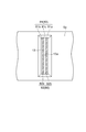
- FIG. 2 is a cross-sectional view taken along line II-II shown in FIG. It is a bottom view of a spectroscopic module. It is a principal part expanded sectional view which shows a light passage hole. It is a principal part enlarged plan view which shows a light passage hole. It is sectional drawing for demonstrating the process of forming a light-incidence side part. It is sectional drawing for demonstrating the process of forming a light emission side part. It is a principal part enlarged plan view corresponding to FIG. 5 which shows the modification of a light passage hole. It is a principal part enlarged plan view corresponding to FIG. 5 which shows the modification of a light passage hole.
- FIG. 5 It is a principal part enlarged plan view corresponding to FIG. 5 which shows the modification of a light passage hole. It is sectional drawing corresponding to FIG. 2 which shows the spectroscopy module which concerns on 2nd Embodiment. It is a principal part expanded sectional view corresponding to FIG. 3 which shows the light passage hole which concerns on 2nd Embodiment.
- the spectroscopic module 1 includes a substrate (main body portion) 2 that transmits light L1 incident from a front surface (predetermined surface) 2a and a substrate 2 that is incident from an incident surface 3a.
- a lens unit (main body unit) 3 that transmits the light L1
- a spectroscopic unit 4 that splits and reflects the light L1 incident on the lens unit 3
- a light detection element 5 that detects the light L2 split by the spectroscopic unit 4. It is equipped with.
- the spectroscopic module 1 splits the light L1 into the light L2 corresponding to a plurality of wavelengths by the spectroscopic unit 4, and detects the light L2 by the light detection element 5, so that the wavelength distribution of the light L1, the intensity of the specific wavelength component, etc. It is a micro-spectral module that measures.
- the substrate 2 is formed in a rectangular plate shape (for example, a total length of 15 to 20 mm, a total width of 11 to 12 mm, and a thickness of 1 to 3 mm) from light-transmitting glass such as BK7, Pyrex (registered trademark), quartz, or plastic. Yes.
- a wiring 11 made of a single layer film such as Al or Au or a laminated film such as Cr—Pt—Au, Ti—Pt—Au, Ti—Ni—Au, Cr—Au is formed. ing.
- the wiring 11 connects a plurality of pad portions 11a arranged at the center of the substrate 2, a plurality of pad portions 11b arranged at one end portion in the longitudinal direction of the substrate 2, and the corresponding pad portions 11a and 11b. A plurality of connecting portions 11c. Further, the wiring 11 has a light reflection preventing layer made of a single layer film such as CrO or a laminated film such as Cr—CrO on the front surface 2 a side of the substrate 2.
- the light absorption layer 13 formed on the front surface 2a of the substrate 2 is a slit (light passage slit) 13a through which the light L1 traveling to the spectroscopic unit 4 passes through a light passage hole 50 (described later) of the light detection element 5.
- Materials for the light absorption layer 13 include black resist, colored resin (silicone, epoxy, acrylic, urethane, polyimide, composite resin, etc.) containing filler (carbon, oxide, etc.), metal such as Cr and Co, or oxidation Examples thereof include metals, laminated films thereof, porous ceramics, metals, and metal oxides.
- the lens unit 3 is made of the same material as the substrate 2, a light-transmitting resin, a light-transmitting inorganic / organic hybrid material, or a light-transmitting low-melting-point glass or plastic for replica molding.
- a shape in which the hemispherical lens is cut off by two planes substantially orthogonal to the incident surface (bottom surface) 3a and substantially parallel to each other to form the side surface 3b for example, a curvature radius of 6 to 10 mm, the incident surface 3a
- the total length is 12 to 18 mm, the entire width of the incident surface 3 a (distance between the side surfaces 3 b) is 6 to 10 mm, and the height is 5 to 8 mm.
- It functions as a lens that forms an image on the detector 5b.
- the lens shape is not limited to a spherical lens, but may be an aspheric lens.
- the spectroscopic unit 4 includes a diffraction layer 6 formed on the outer surface of the lens unit 3, a reflection layer 7 formed on the outer surface of the diffraction layer 6, and a reflection layer 8 that covers the diffraction layer 6 and the reflection layer 7. It is a grating.
- the diffractive layer 6 is formed by arranging a plurality of grating grooves 6 a along the longitudinal direction of the substrate 2, and the extending direction of the grating grooves 6 a substantially coincides with the direction substantially orthogonal to the longitudinal direction of the substrate 2. To do.
- a blazed grating with a sawtooth cross section, a binary grating with a rectangular cross section, a holographic grating with a sinusoidal cross section, etc. are applied, and a photocurable epoxy resin, acrylic resin, or organic-inorganic hybrid resin, etc.
- the optical resin for replica is formed by photocuring.
- the reflective layer 7 has a film shape, and is formed by evaporating Al, Au, or the like on the outer surface of the diffraction layer 6, for example.
- the optical NA of the spectral module 1 can be adjusted by adjusting the area where the reflective layer 7 is formed.
- the passivation layer 8 is in the form of a film, and is formed, for example, by vapor-depositing MgF 2 or SiO 2 on the outer surfaces of the diffraction layer 6 and the reflection layer 7.
- the light detection element 5 is disposed on the front surface 2a of the substrate 2 and has a rectangular shape (for example, a total length of 5 to 10 mm, a total width of 1.5 to 3 mm, a thickness of 0.1 mm). 1 to 0.8 mm) of a semiconductor substrate 5a (substrate portion).
- the semiconductor substrate 5a is made of a crystal material such as Si, GaAs, InGaAs, Ge, SiGe.
- a light detection unit 5b is formed on the surface of the semiconductor substrate 5a on the spectroscopic unit 4 side.
- the light detection unit 5b is a CCD image sensor, a PD array, a CMOS image sensor, or the like, and a direction in which a plurality of channels are substantially orthogonal to the extending direction of the grating grooves 6a of the spectroscopic unit 4 (parallel direction of the grating grooves 6a). It is arranged in.
- a light shielding layer 12 made of Al, Au, or the like is formed on the surface of the semiconductor substrate 5a opposite to the spectroscopic portion 4 by vapor deposition.
- the light detection unit 5b When the light detection unit 5b is a CCD image sensor, light intensity information at a position incident on a two-dimensionally arranged pixel is line binned to obtain light intensity information at a one-dimensional position. The light intensity information at the one-dimensional position is read out in time series. That is, a line of pixels to be line binned becomes one channel.
- the light detection unit 5b is a PD array or a CMOS image sensor
- light intensity information at a position incident on a one-dimensionally arranged pixel is read in time series, so that one pixel becomes one channel.
- the light detection unit 5b is a PD array or a CMOS image sensor and the pixels are two-dimensionally arranged, the pixels lined up in the one-dimensional arrangement direction parallel to the extending direction of the grating grooves 6a of the spectroscopic unit 4 This line becomes one channel.
- the light detection unit 5b is a CCD image sensor, for example, the distance between channels in the arrangement direction is 12.5 ⁇ m, the total channel length (the length of the one-dimensional pixel row to be line binned) is 1 mm, The number 256 is used for the light detection element 5.
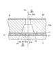
- the semiconductor substrate 5 a is formed with a light passage hole 50 that is arranged in parallel with the light detection unit 5 b in the channel arrangement direction and through which the light L ⁇ b> 1 traveling to the spectroscopic unit 4 passes.
- the light passage hole 50 extends in a direction substantially orthogonal to the front surface 2a of the substrate 2 and is formed by etching in a state of being positioned with high accuracy with respect to the light detection portion 5b.
- the light passage hole 50 includes a light incident side 51 that defines a light incident opening 51a through which light L1 is incident, and a light emission side 52 that defines a light output opening 52a through which the light L1 is emitted.
- the light incident side portion 51 is formed in a substantially square frustum shape so as to be tapered toward the front surface 2 a of the substrate 2, and has a bottom surface 51 b substantially parallel to the front surface 2 a of the substrate 2.
- the light emitting side portion 52 is formed in a substantially square column shape so as to face and connect to the bottom surface 51b of the light incident side portion 51 from the surface on the spectroscopic portion 4 side of the semiconductor substrate 5a.
- the side surface 52b is substantially perpendicular to 2a.
- the light emission side portion 52 has a width H1 (minimum width) that is greater than a width H2 of the slit 13a of the light absorption layer 13 in the channel arrangement direction of the light detection portion 5b (a direction substantially orthogonal to the extending direction of the grating grooves 6a). It is formed to be large.
- an underfill material 15 that transmits at least light L2 is filled between the semiconductor substrate 5a and the substrate 2 or the light absorption layer 13.
- a rectangular annular convex portion 53 is formed on the surface of the semiconductor substrate 5a on the substrate 2 side so as to surround the light emission opening 52a, and the filled underfill material 15 reaches the light emission opening 52a. It is dammed up by the convex part 53 ahead. This prevents the underfill material 15 from entering the light passage hole 50, so that light can be incident on the main body 2 without being refracted or diffused by the underfill material 15.
- the external terminal of the light detection element 5 is electrically connected to the pad portion 11 a exposed from the light absorption layer 13 by face-down bonding via the bumps 14.
- the pad portion 11b is electrically connected to an external electric element (not shown).
- the light detection element 5 is prepared.
- a rectangular ring is formed so as to surround a light emission opening 52a that is planned by performing alkali etching using KOH (potassium hydroxide), TMAH (tetramethylammonium hydroxide), or the like.
- KOH potassium hydroxide
- TMAH tetramethylammonium hydroxide
- the convex portion 53 is formed.
- the light detection part 5b, wiring, and an electrode pad are prepared in the other main surface B side.
- a mask is opened at a predetermined position by photolithography using double-sided alignment with the detection unit 5b as a reference, and alkali etching is performed to form a light incident side portion 51 having a substantially square frustum shape (FIG. 6). reference).
- alkali etching is performed to form a light incident side portion 51 having a substantially square frustum shape (FIG. 6). reference).
- the bottom surface of the light incident side portion 51 is obtained by performing silicon deep dry etching using plasma discharge at a predetermined position on the other main surface B of the semiconductor substrate 5a by photolithography using the detection portion 5b as a reference.
- a light emission side portion 52 having a substantially quadrangular prism shape facing 51b is formed (see FIG. 7).
- the light passage hole 50 extending in the direction substantially orthogonal to the one main surface A of the semiconductor substrate 5a is formed.
- the light shielding layer 12 is formed by vapor-depositing Al, Au, or the like on the one main surface A and the side surface 51c and the bottom surface 51b of the light incident side portion 51, and the wafer is diced on the basis of the detection portion 5b.
- a photodetecting element 5 is prepared.
- the spectroscopic unit 4 is formed in the lens unit 3. Specifically, a light transmissive master grating in which a grating corresponding to the diffraction layer 6 is engraved is pressed against the replica optical resin dropped near the apex of the lens unit 3. Then, the optical resin for replica is cured by irradiating light in this state, and preferably, the diffraction layer 6 having a plurality of grating grooves 6a is formed by performing heat curing for stabilization. Thereafter, the master grating is released, and the reflective layer 7 is formed on the outer surface of the diffractive layer 6 by mask deposition or vapor deposition of Al or Au. Further, the reflective layer 7 is formed on the outer surfaces of the diffractive layer 6 and the reflective layer 7.
- the passivation layer 8 is formed by depositing MgF 2 , SiO 2, or the like by mask evaporation or entire surface evaporation.
- the substrate 2 is prepared, and the light absorption layer 13 having the slits 13 a and the openings 13 b is formed on the front surface 2 a of the substrate 2.
- the slit 13a and the opening 13b are formed so as to have a predetermined positional relationship with respect to the outer edge portion of the substrate 2 serving as a reference portion for positioning the spectroscopic unit 4 on the substrate 2.
- the light detection element 5 On the light absorption layer 13, the light detection element 5 is mounted by face-down bonding. Subsequently, an underfill material 15 is filled between the light detection element 5 and the front surface 2 a of the substrate 2. Thereafter, the spectroscopic module 1 is obtained by adhering the lens unit 3 on which the spectroscopic unit 4 is formed to the rear surface 2b of the substrate 2 with the optical resin agent 18 using the outer edge of the substrate 2 as a reference unit. At this time, the light detecting element 5 and the substrate 2 are electrically connected via the bumps 14.
- the light L1 traveling to the spectroscopic portion 4 is formed so as to face the bottom surface 51b of the light incident side portion 51 that is tapered toward the substrate 2 side when passing through the light passage hole 50. Only the light incident on the emission side portion 52 is emitted from the light emission opening 52a. At this time, the stray light M incident on the bottom surface 51b and the side surface 51c of the light incident side portion 51 is reflected to the light incident opening 51a side, so that the stray light can be prevented from entering the light emitting side portion 52. Therefore, the reliability of the spectroscopic module 1 can be improved.
- the light incident side portion 51 is collectively formed by performing alkali etching on the semiconductor substrate 5 a in a wafer state, so that the time required for preparing the light detecting element 5 can be reduced and reduced. Cost can be reduced.
- the light emission side portion 52 can be formed with high precision by performing silicon deep dry etching from the other main surface B of the semiconductor substrate 5a, the formation of the light passage hole 50 having stable light passage characteristics can be achieved. Thus, the reliability of the spectral module 1 can be improved. Specifically, in the spectroscopic module 1, the light emission side portion 52 is formed from the other main surface B side where the light detection portion 5b is disposed, and thus the light emission side portion 52 with respect to the light detection portion 5b on the same surface. It is possible to increase the position accuracy of the.
- the light exit side 52 of the light passage hole 50 Since the light passing through the light exit side 52 of the light passage hole 50 is diffracted and reflected by the grating groove 6a of the spectroscopic unit 4 and detected by the light detection unit 5b, the light exit side 52 and the light detection unit By improving the positional accuracy with respect to 5b, it becomes possible to improve the reliability of the spectral module 1. Further, the shape of the opening cross section of the light emitting side portion 52 (that is, the shape of the light emitting opening 52a) is optically imaged in the light detecting portion 5b, and the minimum width of the light emitting side portion 52 in the longitudinal direction of the semiconductor substrate 5a. Corresponding to the channels of the light detection section 5b.
- the resolution of the spectroscopic module 1 is greatly affected by the minimum width of the light emitting side portion 52 in the channel arrangement direction. Therefore, by forming the light emission side portion 52 with high precision by performing silicon deep dry etching, it is possible to suppress the variation in resolution for each product and to improve the reliability of the spectral module 1. Become.
- the semiconductor substrate 5a is made of a crystal material such as Si, and the side surface is formed along the (111) crystal plane of the material by performing alkali etching, so that light can be accurately obtained. Since the incident side portion 51 can be formed, the light passing hole 50 can be formed with high accuracy. Therefore, it is possible to improve the reliability of the spectral module 1.
- the resolution of the spectroscopic module 1 is greatly influenced by the minimum width of the slit through which light passes in a direction substantially perpendicular to the extending direction of the grating groove 6a. For this reason, in the direction substantially orthogonal to the extending direction of the grating groove 6a, the spectral module 1 is made by making the width H2 of the slit 13a of the light absorption layer 13 smaller than the minimum width H1 of the light passage hole 50 in the light detection element 5. Resolution can be improved. This is advantageous for improving the reliability of the spectroscopic module 1.
- the light passage hole 60 formed in the light detection element 5 has a light emitting side portion 62 having a side surface 62 b substantially perpendicular to the bottom surface 61 b of the light incident side portion 61 and an elliptical cross section. It may be formed. Further, as shown in FIG. 9, compared with FIG.
- the light emission side portion 72 is extended in the direction substantially perpendicular to the longitudinal direction of the semiconductor substrate 5 a (the extending direction of the grating groove 6 a), and the light incident side portion 71 so that the width of the bottom surface 71b of the light emitting side portion 72 is equal to the width of the opening cross section of the light emitting side portion 72, that is, the side surface 72b of the light emitting side portion 72 and the side surface 71c of the light incident side portion 71 are directly connected. May be.
- FIG. 10 compared to FIG.
- the light emission side portion 82 is further extended, and from the width of the bottom surface 81 b of the light incident side portion 81 in the direction substantially orthogonal to the longitudinal direction of the semiconductor substrate 5 a, It may be formed so that the width of the opening cross section of the light emitting side portion 82 becomes longer.
- the spectroscopic module 21 according to the second embodiment is different from the spectroscopic module 1 according to the first embodiment in the configuration of the light detection element and the point that the wiring board is disposed on the front surface of the substrate.
- a plurality of terminal electrodes 23 are formed on the surface of the photodetecting element 22 opposite to the spectroscopic unit 4.
- Each terminal electrode 23 is connected to the corresponding pad portion 24 a of the wiring substrate 24 by a wire 26.
- the terminal electrode 23 and the wiring board 24 are electrically connected, and the electric signal generated in the light detection unit 22b is transmitted to the outside via the terminal electrode 23, the pad part 24a and the pad part 24b of the wiring board 24. It is taken out.
- the light passage hole 90 formed in the semiconductor substrate 22a is composed of a light incident side portion 91 that defines a light incident opening 91a and a light emission side portion 92 that defines a light emitting opening 92a.
- the light incident side portion 91 has a side surface 91 b that is substantially perpendicular to the front surface 2 a of the substrate 2.
- the light emission side portion 92 is formed in a substantially square frustum shape so as to be widened toward the front surface 2 a of the substrate 2, and has an upper surface 92 b substantially parallel to the front surface 2 a of the substrate 2.
- the light incident side portion 91 is formed in a substantially quadrangular prism shape so as to face the upper surface 92 b of the light emitting side portion 92, and the side surface 91 b is connected to the upper surface 92 b of the light emitting side portion 92.
- the light absorption layer 27 formed on the front surface 2a of the substrate 2 is a slit (light) smaller than the minimum width of the light incident side portion 91 in a direction substantially orthogonal to the extending direction of the grating grooves 6a of the spectroscopic portion 4. Pass slit) 27a.
- the light detection element 22 is prepared.
- a light detection unit 22b, wiring, and electrode pads are prepared on the other main surface B side.
- a light shielding layer 29 is formed by vapor-depositing Al, Au, or the like on an insulating film such as SiO 2 on the other main surface B, and the light detection element 22 is prepared.
- a rectangular annular convex portion 93 is formed so as to surround a light emission opening 92a that is planned by performing alkali etching or dry etching using KOH (potassium hydroxide) or TMAH (tetramethylammonium hydroxide).
- KOH potassium hydroxide
- TMAH tetramethylammonium hydroxide
- a mask is opened at a predetermined position by photolithography using double-sided alignment with respect to one main surface A of the semiconductor substrate 22a with reference to the light detection unit 22b, and KOH (potassium hydroxide) or TMAH ( By performing alkali etching using tetramethylammonium hydroxide, a light emitting side portion 92 having a substantially square frustum shape is formed.
- the bottom surface of the light emission side portion 92 is obtained by performing silicon deep dry etching using plasma discharge at a predetermined position on the other main surface B of the semiconductor substrate 22a by photolithography using the detection portion 22b as a reference.
- a light incident side portion 91 having a substantially quadrangular prism shape connected to 92b is formed.
- a light passage hole 90 extending in a direction substantially orthogonal to one main surface A of the semiconductor substrate 22a is formed.
- the light shielding layer 29 is formed by vapor-depositing Al, Au, or the like on the one main surface A and the side surface 91c and the bottom surface 91b of the light incident side portion 91, and the wafer is diced on the basis of the detection portion 22b.
- a photodetecting element 22 is prepared.
- the light detection element 22 and the outer edge part of the substrate 2 or the alignment mark are used as a reference part, and the other main surface B side of the light detection element 22 and the optical resin material 17 are adhered to the front surface 2a of the substrate 2.
- the terminal electrode 23 of the corresponding light detection element 22 and the pad portion 24 a of the substrate 2 are connected by the wire 26.
- the pad portion 24 a is electrically connected to the terminal pad portion 24 b through the wiring layer 19.
- the light absorption layer made of black resist or the like is disposed on the outer periphery of the light detection element 22, it absorbs disturbance light and unnecessary reflected light as a signal from the spectroscopic unit 4, and is reliable. Can be secured.
- the spectroscopic module 21 is obtained by adhering the lens unit 3 on which the spectroscopic unit 4 is formed to the rear surface 2b of the substrate 2 with the optical resin agent 18 using the outer edge of the substrate 2 as a reference unit.
- the light emitting side portion 92 is collectively formed by performing alkali etching on the semiconductor substrate 22a in the wafer state, so that the light detecting element 22 Time reduction and cost reduction in the preparation process can be achieved. Further, since the light emission side portion 52 can be formed with high precision by performing silicon deep dry etching from the other main surface B of the semiconductor substrate 5a, the formation of the light passage hole 50 having stable light passage characteristics can be achieved. Thus, the reliability of the spectral module 1 can be improved.
- the present invention is not limited to the embodiment described above.
- the shapes of the light incident side portion in the first embodiment and the light emission side portion in the second embodiment are not limited to a substantially square frustum shape, and a bottom surface (upper surface) substantially parallel to the front surface 2a of the substrate 2 is used. It has only to have a shape that has a taper toward the front surface 2a.
- the shape of the light emitting side portion in the first embodiment and the light incident side portion in the second embodiment is not limited to a substantially quadrangular prism shape
- the substrate 2 may have a side surface substantially perpendicular to the front surface 2a and be formed so as to face the bottom surface (upper surface) of the paired light incident side portion (light emitting side portion).
- the light passage hole is not limited to a mode in which the light incident side portion and the light emitting side portion are directly connected to each other, and an intermediate portion (for example, a portion having a different inclination angle of the side surface or shape of the opening cross section) is provided. It may be done.
- the light incident side portion in the first embodiment and the light emission side portion in the second embodiment are not limited to being formed by alkali etching, but may be formed by various wet etching or dry etching. It ’s fine.
- the light emitting side portion in the first embodiment and the light incident side portion in the second embodiment are not limited to being formed by silicon deep dry etching, but may be any form formed by various dry etching. good.
- the configuration of the light passage hole in the second embodiment may be adopted, and in the second embodiment, the configuration of the light passage hole in the first embodiment is adopted. May be.
- a highly reliable spectroscopic module can be provided.
- Light exit side 51a, 61a, 71a, 81a, 91a ...
- Light incident aperture 51b, 61b, 71b, 81b ...
- 51c, 61c , 71c, 81c, 92c ... side face, 52a, 62a, 72a, 82a, 92a ... light exit opening, 92b ... top face (bottom face), 52b, 62b, 72b, 82b, 91b ... side face, A ... one main face, B ... the other main surface.
Abstract
Description
[第1の実施形態]
[第2の実施形態]
基板2の前面2aと略垂直な側面を有し、且つ、対となる光入射側部(光出射側部)の底面(上面)に対向するように形成されていれば良い。
Claims (4)
- 光を透過させる本体部と、
前記本体部の所定の面側から前記本体部に入射した光を分光すると共に前記所定の面側に反射する分光部と、
前記所定の面上に配置され、前記分光部によって分光された光を検出する光検出素子と、を備え、
前記光検出素子は、前記分光部に進行する光が通過する光通過孔が形成された基板部を有し、
前記光通過孔は、光入射開口を画定する光入射側部、及び光出射開口を画定する光出射側部を含み、
前記光入射側部は、前記所定の面と略平行な底面を有し且つ前記所定の面に向かって先細りとなるように形成され、
前記光出射側部は、前記所定の面と略垂直な側面を有し且つ前記底面と対向するように形成されたことを特徴とする分光モジュール。 - 前記光検出素子と前記所定の面との間には、光を吸収する光吸収層が形成されており、
前記光吸収層は、前記光通過孔を介して前記分光部に進行する光が通過する光通過スリットを有し、
前記光通過スリットの幅は、前記分光部に形成されたグレーティング溝の延在方向と略直交する方向において前記光出射側部の最小幅より小さくなっていることを特徴とする請求項1に記載の分光モジュール。 - 前記基板部は、結晶材料からなり、
前記光入射側部の側面は、(111)結晶面に沿って形成されていることを特徴とする請求項1に記載の分光モジュール。 - 光を透過させる本体部と、前記本体部の所定の面側から前記本体部に入射した光を分光すると共に前記所定の面側に反射する分光部と、前記分光部によって分光された光を検出する光検出素子と、を備える分光モジュールの製造方法であって、
光通過孔が形成された基板部を有する前記光検出素子を用意する光検出素子用意工程と、
前記光検出素子用意工程において用意した前記光検出素子と前記分光部とを前記本体部上に配置する配置工程と、を備え、
前記光検出素子用意工程は、前記基板部の一方の主面側からウェットエッチングを施すことにより、前記一方の主面と略平行な底面を有し且つ他方の主面に向かって先細りとなるように、前記光通過孔の光入射開口を画定する光入射側部を形成する光入射側部形成工程と、
前記光入射側部形成工程の後に、前記基板部の他方の主面側からドライエッチングを施すことにより、前記一方の主面と略垂直な側面を有し且つ前記底面と対向するように、前記光通過孔の光出射開口を画定する光出射側部を形成する光出射側部形成工程と、を含むことを特徴とする分光モジュールの製造方法。
Priority Applications (4)
| Application Number | Priority Date | Filing Date | Title |
|---|---|---|---|
| US12/992,473 US8604412B2 (en) | 2008-05-15 | 2009-05-07 | Spectral module and method for manufacturing spectral module |
| CN2009801172801A CN102027342B (zh) | 2008-05-15 | 2009-05-07 | 分光模块以及分光模块的制造方法 |
| EP09746529.8A EP2287577B1 (en) | 2008-05-15 | 2009-05-07 | Spectral module and method for manufacturing spectral module |
| US13/964,472 US8742320B2 (en) | 2008-05-15 | 2013-08-12 | Spectral module and method for manufacturing spectral module |
Applications Claiming Priority (4)
| Application Number | Priority Date | Filing Date | Title |
|---|---|---|---|
| JP2008-128687 | 2008-05-15 | ||
| JP2008128687 | 2008-05-15 | ||
| JP2008-311087 | 2008-12-05 | ||
| JP2008311087A JP5207938B2 (ja) | 2008-05-15 | 2008-12-05 | 分光モジュール及び分光モジュールの製造方法 |
Related Child Applications (2)
| Application Number | Title | Priority Date | Filing Date |
|---|---|---|---|
| US12/992,473 A-371-Of-International US8604412B2 (en) | 2008-05-15 | 2009-05-07 | Spectral module and method for manufacturing spectral module |
| US13/964,472 Continuation US8742320B2 (en) | 2008-05-15 | 2013-08-12 | Spectral module and method for manufacturing spectral module |
Publications (1)
| Publication Number | Publication Date |
|---|---|
| WO2009139322A1 true WO2009139322A1 (ja) | 2009-11-19 |
Family
ID=41318693
Family Applications (1)
| Application Number | Title | Priority Date | Filing Date |
|---|---|---|---|
| PCT/JP2009/058639 WO2009139322A1 (ja) | 2008-05-15 | 2009-05-07 | 分光モジュール及び分光モジュールの製造方法 |
Country Status (6)
| Country | Link |
|---|---|
| US (2) | US8604412B2 (ja) |
| EP (1) | EP2287577B1 (ja) |
| JP (1) | JP5207938B2 (ja) |
| KR (1) | KR101617473B1 (ja) |
| CN (2) | CN103383284B (ja) |
| WO (1) | WO2009139322A1 (ja) |
Families Citing this family (37)
| Publication number | Priority date | Publication date | Assignee | Title |
|---|---|---|---|---|
| JP2009300422A (ja) * | 2008-05-15 | 2009-12-24 | Hamamatsu Photonics Kk | 分光モジュール |
| JP5205242B2 (ja) * | 2008-05-15 | 2013-06-05 | 浜松ホトニクス株式会社 | 分光器の製造方法 |
| JP2009300418A (ja) | 2008-05-15 | 2009-12-24 | Hamamatsu Photonics Kk | 分光モジュール |
| JP5205240B2 (ja) * | 2008-05-15 | 2013-06-05 | 浜松ホトニクス株式会社 | 分光モジュールの製造方法及び分光モジュール |
| JP2009300417A (ja) * | 2008-05-15 | 2009-12-24 | Hamamatsu Photonics Kk | 分光モジュールの製造方法及び分光モジュール |
| JP5205243B2 (ja) * | 2008-05-15 | 2013-06-05 | 浜松ホトニクス株式会社 | 分光器 |
| JP5205241B2 (ja) * | 2008-05-15 | 2013-06-05 | 浜松ホトニクス株式会社 | 分光モジュール |
| JP5415060B2 (ja) * | 2008-05-15 | 2014-02-12 | 浜松ホトニクス株式会社 | 分光モジュール |
| JP5205238B2 (ja) * | 2008-05-15 | 2013-06-05 | 浜松ホトニクス株式会社 | 分光モジュール |
| JP5512961B2 (ja) * | 2008-05-15 | 2014-06-04 | 浜松ホトニクス株式会社 | 分光モジュール及びその製造方法 |
| JP5335729B2 (ja) | 2010-04-01 | 2013-11-06 | 浜松ホトニクス株式会社 | 分光モジュール |
| JP5325829B2 (ja) | 2010-04-01 | 2013-10-23 | 浜松ホトニクス株式会社 | 分光モジュール |
| JP2014532873A (ja) | 2011-11-03 | 2014-12-08 | ベリフード リミテッド | エンドユーザ食品分析のための低費用分光分析システム |
| JP5988690B2 (ja) | 2012-05-18 | 2016-09-07 | 浜松ホトニクス株式会社 | 分光センサ |
| JP5926610B2 (ja) | 2012-05-18 | 2016-05-25 | 浜松ホトニクス株式会社 | 分光センサ |
| JP5875936B2 (ja) | 2012-05-18 | 2016-03-02 | 浜松ホトニクス株式会社 | 分光センサ |
| JP6234667B2 (ja) * | 2012-08-06 | 2017-11-22 | 浜松ホトニクス株式会社 | 光学素子及びその製造方法 |
| CN105593651B (zh) | 2013-08-02 | 2019-06-07 | 威利食品有限公司 | 光谱测定系统和方法、光谱设备和系统 |
| JP2015106106A (ja) | 2013-12-02 | 2015-06-08 | セイコーエプソン株式会社 | 電子デバイスおよび電子機器 |
| EP3090239A4 (en) | 2014-01-03 | 2018-01-10 | Verifood Ltd. | Spectrometry systems, methods, and applications |
| JP6251073B2 (ja) * | 2014-02-05 | 2017-12-20 | 浜松ホトニクス株式会社 | 分光器、及び分光器の製造方法 |
| EP3209983A4 (en) | 2014-10-23 | 2018-06-27 | Verifood Ltd. | Accessories for handheld spectrometer |
| WO2016125164A2 (en) | 2015-02-05 | 2016-08-11 | Verifood, Ltd. | Spectrometry system applications |
| WO2016125165A2 (en) | 2015-02-05 | 2016-08-11 | Verifood, Ltd. | Spectrometry system with visible aiming beam |
| WO2016162865A1 (en) | 2015-04-07 | 2016-10-13 | Verifood, Ltd. | Detector for spectrometry system |
| US10066990B2 (en) | 2015-07-09 | 2018-09-04 | Verifood, Ltd. | Spatially variable filter systems and methods |
| US10203246B2 (en) | 2015-11-20 | 2019-02-12 | Verifood, Ltd. | Systems and methods for calibration of a handheld spectrometer |
| US10254215B2 (en) | 2016-04-07 | 2019-04-09 | Verifood, Ltd. | Spectrometry system applications |
| EP3488204A4 (en) | 2016-07-20 | 2020-07-22 | Verifood Ltd. | ACCESSORIES FOR HANDLABLE SPECTROMETERS |
| US10791933B2 (en) | 2016-07-27 | 2020-10-06 | Verifood, Ltd. | Spectrometry systems, methods, and applications |
| US10368411B2 (en) * | 2016-09-20 | 2019-07-30 | Bolb Inc. | Ultraviolet light module having output power control mechanism |
| EP3372966B1 (en) * | 2017-03-10 | 2021-09-01 | Hitachi High-Tech Analytical Science Limited | A portable analyzer using optical emission spectoscopy |
| JP2019039738A (ja) * | 2017-08-24 | 2019-03-14 | セイコーエプソン株式会社 | 光学モジュール及び電子機器 |
| KR102498122B1 (ko) | 2017-11-21 | 2023-02-09 | 삼성전자주식회사 | 분광 장치와, 분광 방법, 및 생체신호 측정장치 |
| CN110658603B (zh) * | 2018-06-29 | 2021-08-06 | 台湾超微光学股份有限公司 | 一种转接组件、光学前端结合装置以及光谱仪 |
| CN108956467B (zh) * | 2018-08-09 | 2022-04-22 | 京东方科技集团股份有限公司 | 一种微流控芯片及其工作方法 |
| CN111175890B (zh) * | 2018-11-12 | 2022-04-19 | 国科光芯(海宁)科技股份有限公司 | 一种光学相控阵集成芯片 |
Citations (6)
| Publication number | Priority date | Publication date | Assignee | Title |
|---|---|---|---|---|
| JPH04294223A (ja) | 1990-12-04 | 1992-10-19 | Carl Zeiss:Fa | ダイオード列型分光分析器 |
| JPH06167637A (ja) * | 1992-11-30 | 1994-06-14 | Hitachi Ltd | 多芯光コネクタ |
| JP2000065642A (ja) | 1998-03-11 | 2000-03-03 | Gretag Macbeth Ag | スペクトロメ―タ |
| JP2003139611A (ja) * | 2001-11-06 | 2003-05-14 | Olympus Optical Co Ltd | 分光光度計 |
| JP2004354176A (ja) | 2003-05-28 | 2004-12-16 | Hamamatsu Photonics Kk | 光検出器及びそれを用いた分光器 |
| WO2008149940A1 (ja) * | 2007-06-08 | 2008-12-11 | Hamamatsu Photonics K.K. | 分光モジュール |
Family Cites Families (71)
| Publication number | Priority date | Publication date | Assignee | Title |
|---|---|---|---|---|
| US4259014A (en) | 1979-04-03 | 1981-03-31 | Princeton Applied Research Corporation | Fiber optic polychromator |
| DE3509131A1 (de) | 1985-03-14 | 1986-09-18 | Fa. Carl Zeiss, 7920 Heidenheim | Verfahren zur justierten montage der optischen bauteile eines optischen geraetes |
| US5068223A (en) * | 1985-09-09 | 1991-11-26 | Board Of Regents, University Of Texas System | Hydrophobic peptide esters and amides |
| JP2592081B2 (ja) | 1987-12-28 | 1997-03-19 | スズキ株式会社 | 自動二輪車等のマフラ |
| JPH04287001A (ja) | 1991-03-15 | 1992-10-12 | Sekinosu Kk | 光回折格子の製造方法 |
| DE69304315T2 (de) * | 1993-06-09 | 1997-01-16 | Hewlett Packard Gmbh | Regelbare optische Komponente |
| JPH08145794A (ja) | 1994-11-17 | 1996-06-07 | Shimadzu Corp | 分光器 |
| US6224912B1 (en) | 1996-04-03 | 2001-05-01 | The Rogo Institute | Cancer-cell proliferation-suppressing material produced by cancer cells restricted by entrapment |
| US5995221A (en) | 1997-02-28 | 1999-11-30 | Instruments S.A., Inc. | Modified concentric spectrograph |
| US6303934B1 (en) | 1997-04-10 | 2001-10-16 | James T. Daly | Monolithic infrared spectrometer apparatus and methods |
| DE19717015A1 (de) | 1997-04-23 | 1998-10-29 | Inst Mikrotechnik Mainz Gmbh | Miniaturisiertes optisches Bauelement sowie Verfahren zu seiner Herstellung |
| DE19717014A1 (de) | 1997-04-23 | 1998-10-29 | Inst Mikrotechnik Mainz Gmbh | Verfahren und Form zur Herstellung miniaturisierter Formenkörper |
| DE69712115T2 (de) | 1997-11-28 | 2002-09-26 | Hamamatsu Photonics Kk | Festkörperbildaufnahmevorrichtung für analysevorrichtung |
| US6249346B1 (en) | 1998-12-21 | 2001-06-19 | Xerox Corporation | Monolithic spectrophotometer |
| US6608679B1 (en) | 1998-12-21 | 2003-08-19 | Xerox Corporation | Spectrophotometric analysis of input light |
| JP2000269472A (ja) | 1999-03-15 | 2000-09-29 | Canon Inc | 撮像装置 |
| EP1041372B1 (de) | 1999-04-01 | 2006-03-01 | Gretag-Macbeth AG | Spektrometer |
| US6538736B1 (en) | 1999-12-01 | 2003-03-25 | Hach Company | Concentric spectrometer with mitigation of internal specular reflections |
| AU2001276875A1 (en) | 2000-07-11 | 2002-01-21 | Ibsen Photonics | Monitoring apparatus for optical transmission systems |
| CN1296684C (zh) | 2000-07-28 | 2007-01-24 | 大塚电子株式会社 | 光谱检测设备 |
| US6657723B2 (en) | 2000-12-13 | 2003-12-02 | International Business Machines Corporation | Multimode planar spectrographs for wavelength demultiplexing and methods of fabrication |
| CN100354699C (zh) | 2001-08-02 | 2007-12-12 | 伊吉斯半导体公司 | 可调谐光学仪器 |
| JP3912111B2 (ja) | 2002-01-09 | 2007-05-09 | 富士通株式会社 | 波長多重双方向光伝送モジュール |
| JP3818441B2 (ja) | 2002-02-20 | 2006-09-06 | 日本電信電話株式会社 | 基板実装構造及び半導体装置 |
| CN1193213C (zh) * | 2002-05-13 | 2005-03-16 | 重庆大学 | 集成化微型光谱仪 |
| JP4221965B2 (ja) | 2002-07-22 | 2009-02-12 | 日立電線株式会社 | 回折格子、波長合分波器及びこれらを用いた波長多重信号光伝送モジュール |
| US6885107B2 (en) | 2002-08-29 | 2005-04-26 | Micron Technology, Inc. | Flip-chip image sensor packages and methods of fabrication |
| WO2004027493A1 (ja) | 2002-09-20 | 2004-04-01 | Nippon Sheet Glass Company, Limited | 回折格子を用いた分光装置 |
| FR2847978B1 (fr) | 2002-12-02 | 2005-12-02 | Technologie Optique Et Etudes | Spectrometre compact a composant optique monolithique |
| JP2004191246A (ja) | 2002-12-12 | 2004-07-08 | Matsushita Electric Ind Co Ltd | 凹凸検出センサ |
| DE10304312A1 (de) | 2003-02-04 | 2004-08-12 | Carl Zeiss Jena Gmbh | Kompakt-Spektrometer |
| CN100438054C (zh) | 2003-03-10 | 2008-11-26 | 浜松光子学株式会社 | 光电二极管阵列及其制造方法和放射线检测器 |
| JP2004309146A (ja) | 2003-04-02 | 2004-11-04 | Olympus Corp | 分光光度計 |
| US7623235B2 (en) | 2004-03-20 | 2009-11-24 | Seng-Tiong Ho | Curved grating spectrometer with very high wavelength resolution |
| US7283233B1 (en) | 2004-03-20 | 2007-10-16 | Seng-Tiong Ho | Curved grating spectrometer with very high wavelength resolution |
| JP4627410B2 (ja) | 2004-04-20 | 2011-02-09 | 浜松ホトニクス株式会社 | 分光器を用いた測定装置 |
| JP4720120B2 (ja) | 2004-07-14 | 2011-07-13 | ソニー株式会社 | 半導体イメージセンサ・モジュール |
| JP4473665B2 (ja) | 2004-07-16 | 2010-06-02 | 浜松ホトニクス株式会社 | 分光器 |
| EP1779074A2 (en) | 2004-07-26 | 2007-05-02 | Danmarks Tekniske Universitet | On-chip spectroscopy |
| JP4576961B2 (ja) | 2004-09-28 | 2010-11-10 | 株式会社島津製作所 | レプリカ回折格子の製造方法 |
| JP2006322841A (ja) * | 2005-05-19 | 2006-11-30 | Shimadzu Corp | 分光測定方法及び分光光度計 |
| US7330258B2 (en) | 2005-05-27 | 2008-02-12 | Innovative Technical Solutions, Inc. | Spectrometer designs |
| US7289220B2 (en) | 2005-10-14 | 2007-10-30 | Board Of Regents, The University Of Texas System | Broadband cavity spectrometer apparatus and method for determining the path length of an optical structure |
| JP4811032B2 (ja) | 2006-01-30 | 2011-11-09 | 株式会社島津製作所 | 反射型レプリカ光学素子 |
| US7697137B2 (en) | 2006-04-28 | 2010-04-13 | Corning Incorporated | Monolithic Offner spectrometer |
| EP1882916A1 (en) | 2006-07-20 | 2008-01-30 | Interuniversitair Microelektronica Centrum | Compact catadioptric spectrometer |
| JP5182093B2 (ja) | 2006-09-06 | 2013-04-10 | 株式会社ニコン | 光学装置、露光装置、並びにデバイス製造方法 |
| JP4490406B2 (ja) | 2006-10-11 | 2010-06-23 | 浜松ホトニクス株式会社 | 固体撮像装置 |
| JP4905193B2 (ja) | 2007-03-16 | 2012-03-28 | コニカミノルタセンシング株式会社 | 凹面回折ミラー及びこれを用いた分光装置 |
| JP5094742B2 (ja) | 2007-06-08 | 2012-12-12 | 浜松ホトニクス株式会社 | 分光器 |
| JP4887221B2 (ja) * | 2007-06-08 | 2012-02-29 | 浜松ホトニクス株式会社 | 分光モジュール |
| WO2008149930A1 (ja) | 2007-06-08 | 2008-12-11 | Hamamatsu Photonics K.K. | 分光モジュール |
| JP4891841B2 (ja) | 2007-06-08 | 2012-03-07 | 浜松ホトニクス株式会社 | 分光モジュール |
| TWI342862B (en) | 2008-01-31 | 2011-06-01 | Univ Nat Taiwan | Method of micro/nano imprinting |
| EP2801802A1 (en) | 2008-03-04 | 2014-11-12 | Hamamatsu Photonics K.K. | Spectroscopy module |
| JP5111163B2 (ja) | 2008-03-04 | 2012-12-26 | 浜松ホトニクス株式会社 | 分光器 |
| JP5205242B2 (ja) | 2008-05-15 | 2013-06-05 | 浜松ホトニクス株式会社 | 分光器の製造方法 |
| JP5512961B2 (ja) | 2008-05-15 | 2014-06-04 | 浜松ホトニクス株式会社 | 分光モジュール及びその製造方法 |
| JP5415060B2 (ja) | 2008-05-15 | 2014-02-12 | 浜松ホトニクス株式会社 | 分光モジュール |
| JP2009300418A (ja) | 2008-05-15 | 2009-12-24 | Hamamatsu Photonics Kk | 分光モジュール |
| JP5074291B2 (ja) | 2008-05-15 | 2012-11-14 | 浜松ホトニクス株式会社 | 分光モジュール |
| JP5205243B2 (ja) | 2008-05-15 | 2013-06-05 | 浜松ホトニクス株式会社 | 分光器 |
| JP5205240B2 (ja) | 2008-05-15 | 2013-06-05 | 浜松ホトニクス株式会社 | 分光モジュールの製造方法及び分光モジュール |
| JP5205238B2 (ja) | 2008-05-15 | 2013-06-05 | 浜松ホトニクス株式会社 | 分光モジュール |
| JP5205239B2 (ja) | 2008-05-15 | 2013-06-05 | 浜松ホトニクス株式会社 | 分光器 |
| JP5411778B2 (ja) | 2009-04-30 | 2014-02-12 | キヤノン株式会社 | 分光測色装置、およびそれを用いた画像形成装置 |
| JP2010261767A (ja) | 2009-05-01 | 2010-11-18 | Canon Inc | 分光装置及びそれを有する画像形成装置 |
| JP5669434B2 (ja) | 2009-05-09 | 2015-02-12 | キヤノン株式会社 | 回折素子及び回折素子の製造方法及びそれを用いた分光器 |
| JP5421684B2 (ja) | 2009-07-29 | 2014-02-19 | キヤノン株式会社 | 回折光学素子、それを用いた分光測色装置および画像形成装置 |
| DE102009046831B4 (de) | 2009-11-18 | 2015-02-12 | Fraunhofer-Gesellschaft zur Förderung der angewandten Forschung e.V. | Strahlungserzeugungsvorrichtung zum Erzeugen einer elektromagnetischen Strahlung mit einer einstellbaren spektralen Zusammensetzung und Verfahren zur Herstellung derselben |
| JP5335729B2 (ja) | 2010-04-01 | 2013-11-06 | 浜松ホトニクス株式会社 | 分光モジュール |
-
2008
- 2008-12-05 JP JP2008311087A patent/JP5207938B2/ja active Active
-
2009
- 2009-05-07 WO PCT/JP2009/058639 patent/WO2009139322A1/ja active Application Filing
- 2009-05-07 CN CN201310278543.5A patent/CN103383284B/zh active Active
- 2009-05-07 US US12/992,473 patent/US8604412B2/en active Active
- 2009-05-07 EP EP09746529.8A patent/EP2287577B1/en active Active
- 2009-05-07 CN CN2009801172801A patent/CN102027342B/zh active Active
- 2009-05-07 KR KR1020107015310A patent/KR101617473B1/ko active IP Right Review Request
-
2013
- 2013-08-12 US US13/964,472 patent/US8742320B2/en active Active
Patent Citations (6)
| Publication number | Priority date | Publication date | Assignee | Title |
|---|---|---|---|---|
| JPH04294223A (ja) | 1990-12-04 | 1992-10-19 | Carl Zeiss:Fa | ダイオード列型分光分析器 |
| JPH06167637A (ja) * | 1992-11-30 | 1994-06-14 | Hitachi Ltd | 多芯光コネクタ |
| JP2000065642A (ja) | 1998-03-11 | 2000-03-03 | Gretag Macbeth Ag | スペクトロメ―タ |
| JP2003139611A (ja) * | 2001-11-06 | 2003-05-14 | Olympus Optical Co Ltd | 分光光度計 |
| JP2004354176A (ja) | 2003-05-28 | 2004-12-16 | Hamamatsu Photonics Kk | 光検出器及びそれを用いた分光器 |
| WO2008149940A1 (ja) * | 2007-06-08 | 2008-12-11 | Hamamatsu Photonics K.K. | 分光モジュール |
Also Published As
| Publication number | Publication date |
|---|---|
| CN103383284B (zh) | 2016-02-10 |
| EP2287577B1 (en) | 2020-12-09 |
| JP5207938B2 (ja) | 2013-06-12 |
| CN102027342A (zh) | 2011-04-20 |
| EP2287577A4 (en) | 2015-03-18 |
| US8604412B2 (en) | 2013-12-10 |
| CN103383284A (zh) | 2013-11-06 |
| CN102027342B (zh) | 2013-08-07 |
| KR101617473B1 (ko) | 2016-05-02 |
| JP2009300424A (ja) | 2009-12-24 |
| US20110075143A1 (en) | 2011-03-31 |
| EP2287577A1 (en) | 2011-02-23 |
| US20130329225A1 (en) | 2013-12-12 |
| KR20110008155A (ko) | 2011-01-26 |
| US8742320B2 (en) | 2014-06-03 |
Similar Documents
| Publication | Publication Date | Title |
|---|---|---|
| JP5207938B2 (ja) | 分光モジュール及び分光モジュールの製造方法 | |
| JP5512961B2 (ja) | 分光モジュール及びその製造方法 | |
| JP5205240B2 (ja) | 分光モジュールの製造方法及び分光モジュール | |
| JP5415060B2 (ja) | 分光モジュール | |
| JP5205239B2 (ja) | 分光器 | |
| JP5205238B2 (ja) | 分光モジュール | |
| JP5335729B2 (ja) | 分光モジュール | |
| JP5205241B2 (ja) | 分光モジュール | |
| JP5325829B2 (ja) | 分光モジュール | |
| JP5718091B2 (ja) | 分光モジュール | |
| JP2009300418A (ja) | 分光モジュール | |
| WO2009139321A1 (ja) | 分光モジュール | |
| JP5235250B2 (ja) | 分光モジュール | |
| WO2009139320A1 (ja) | 分光モジュール | |
| JP5113947B2 (ja) | 分光モジュール |
Legal Events
| Date | Code | Title | Description |
|---|---|---|---|
| WWE | Wipo information: entry into national phase |
Ref document number: 200980117280.1 Country of ref document: CN |
|
| 121 | Ep: the epo has been informed by wipo that ep was designated in this application |
Ref document number: 09746529 Country of ref document: EP Kind code of ref document: A1 |
|
| ENP | Entry into the national phase |
Ref document number: 20107015310 Country of ref document: KR Kind code of ref document: A |
|
| NENP | Non-entry into the national phase |
Ref country code: DE |
|
| WWE | Wipo information: entry into national phase |
Ref document number: 2009746529 Country of ref document: EP |
|
| WWE | Wipo information: entry into national phase |
Ref document number: 12992473 Country of ref document: US |