WO2009139272A1 - 多層セラミック基板およびその製造方法 - Google Patents
多層セラミック基板およびその製造方法 Download PDFInfo
- Publication number
- WO2009139272A1 WO2009139272A1 PCT/JP2009/057896 JP2009057896W WO2009139272A1 WO 2009139272 A1 WO2009139272 A1 WO 2009139272A1 JP 2009057896 W JP2009057896 W JP 2009057896W WO 2009139272 A1 WO2009139272 A1 WO 2009139272A1
- Authority
- WO
- WIPO (PCT)
- Prior art keywords
- layer
- thermal expansion
- expansion coefficient
- low thermal
- wall portion
- Prior art date
Links
- 239000000919 ceramic Substances 0.000 title claims abstract description 187
- 239000000758 substrate Substances 0.000 title claims abstract description 103
- 238000004519 manufacturing process Methods 0.000 title claims description 21
- 238000010304 firing Methods 0.000 claims abstract description 45
- 239000010410 layer Substances 0.000 claims description 368
- 230000002093 peripheral effect Effects 0.000 claims description 84
- 239000011229 interlayer Substances 0.000 claims description 64
- 239000000843 powder Substances 0.000 claims description 36
- 229910010272 inorganic material Inorganic materials 0.000 claims description 23
- 239000011147 inorganic material Substances 0.000 claims description 23
- 229910010293 ceramic material Inorganic materials 0.000 claims description 19
- 239000002131 composite material Substances 0.000 claims description 19
- 239000000463 material Substances 0.000 claims description 17
- 238000005245 sintering Methods 0.000 claims description 14
- 238000010030 laminating Methods 0.000 claims description 6
- 230000008595 infiltration Effects 0.000 claims 1
- 238000001764 infiltration Methods 0.000 claims 1
- 238000000034 method Methods 0.000 abstract description 16
- 238000001816 cooling Methods 0.000 abstract description 4
- 230000006835 compression Effects 0.000 abstract 1
- 238000007906 compression Methods 0.000 abstract 1
- 239000011521 glass Substances 0.000 description 23
- 229910004298 SiO 2 Inorganic materials 0.000 description 19
- 239000004020 conductor Substances 0.000 description 19
- 229910018072 Al 2 O 3 Inorganic materials 0.000 description 18
- 239000000203 mixture Substances 0.000 description 9
- 230000000052 comparative effect Effects 0.000 description 8
- 239000000945 filler Substances 0.000 description 8
- 239000013078 crystal Substances 0.000 description 6
- 230000000694 effects Effects 0.000 description 6
- 239000005388 borosilicate glass Substances 0.000 description 5
- 239000011230 binding agent Substances 0.000 description 4
- 239000002002 slurry Substances 0.000 description 4
- ZTQSAGDEMFDKMZ-UHFFFAOYSA-N Butyraldehyde Chemical compound CCCC=O ZTQSAGDEMFDKMZ-UHFFFAOYSA-N 0.000 description 3
- 230000006378 damage Effects 0.000 description 3
- 230000007423 decrease Effects 0.000 description 3
- 239000003960 organic solvent Substances 0.000 description 3
- 239000004014 plasticizer Substances 0.000 description 3
- 230000001629 suppression Effects 0.000 description 3
- 230000008602 contraction Effects 0.000 description 2
- 230000007547 defect Effects 0.000 description 2
- 230000002401 inhibitory effect Effects 0.000 description 2
- 238000009413 insulation Methods 0.000 description 2
- 230000035515 penetration Effects 0.000 description 2
- 238000007747 plating Methods 0.000 description 2
- 230000002829 reductive effect Effects 0.000 description 2
- 238000005728 strengthening Methods 0.000 description 2
- 239000001856 Ethyl cellulose Substances 0.000 description 1
- ZZSNKZQZMQGXPY-UHFFFAOYSA-N Ethyl cellulose Chemical compound CCOCC1OC(OC)C(OCC)C(OCC)C1OC1C(O)C(O)C(OC)C(CO)O1 ZZSNKZQZMQGXPY-UHFFFAOYSA-N 0.000 description 1
- 229910015868 MSiO Inorganic materials 0.000 description 1
- BQCADISMDOOEFD-UHFFFAOYSA-N Silver Chemical compound [Ag] BQCADISMDOOEFD-UHFFFAOYSA-N 0.000 description 1
- 229910010413 TiO 2 Inorganic materials 0.000 description 1
- PNEYBMLMFCGWSK-UHFFFAOYSA-N aluminium oxide Inorganic materials [O-2].[O-2].[O-2].[Al+3].[Al+3] PNEYBMLMFCGWSK-UHFFFAOYSA-N 0.000 description 1
- 238000005422 blasting Methods 0.000 description 1
- 239000003990 capacitor Substances 0.000 description 1
- 230000003247 decreasing effect Effects 0.000 description 1
- 230000032798 delamination Effects 0.000 description 1
- 238000007606 doctor blade method Methods 0.000 description 1
- 238000001035 drying Methods 0.000 description 1
- 230000003628 erosive effect Effects 0.000 description 1
- 235000019325 ethyl cellulose Nutrition 0.000 description 1
- 229920001249 ethyl cellulose Polymers 0.000 description 1
- 239000011148 porous material Substances 0.000 description 1
- 239000002244 precipitate Substances 0.000 description 1
- 238000001556 precipitation Methods 0.000 description 1
- 229910000679 solder Inorganic materials 0.000 description 1
- 238000007711 solidification Methods 0.000 description 1
- 230000008023 solidification Effects 0.000 description 1
- 239000000126 substance Substances 0.000 description 1
- 150000003505 terpenes Chemical class 0.000 description 1
- 235000007586 terpenes Nutrition 0.000 description 1
- 238000004506 ultrasonic cleaning Methods 0.000 description 1
Images


Classifications
-
- H—ELECTRICITY
- H05—ELECTRIC TECHNIQUES NOT OTHERWISE PROVIDED FOR
- H05K—PRINTED CIRCUITS; CASINGS OR CONSTRUCTIONAL DETAILS OF ELECTRIC APPARATUS; MANUFACTURE OF ASSEMBLAGES OF ELECTRICAL COMPONENTS
- H05K1/00—Printed circuits
- H05K1/18—Printed circuits structurally associated with non-printed electric components
- H05K1/182—Printed circuits structurally associated with non-printed electric components associated with components mounted in the printed circuit board, e.g. insert mounted components [IMC]
- H05K1/183—Components mounted in and supported by recessed areas of the printed circuit board
-
- B—PERFORMING OPERATIONS; TRANSPORTING
- B28—WORKING CEMENT, CLAY, OR STONE
- B28B—SHAPING CLAY OR OTHER CERAMIC COMPOSITIONS; SHAPING SLAG; SHAPING MIXTURES CONTAINING CEMENTITIOUS MATERIAL, e.g. PLASTER
- B28B11/00—Apparatus or processes for treating or working the shaped or preshaped articles
- B28B11/24—Apparatus or processes for treating or working the shaped or preshaped articles for curing, setting or hardening
- B28B11/243—Setting, e.g. drying, dehydrating or firing ceramic articles
-
- B—PERFORMING OPERATIONS; TRANSPORTING
- B32—LAYERED PRODUCTS
- B32B—LAYERED PRODUCTS, i.e. PRODUCTS BUILT-UP OF STRATA OF FLAT OR NON-FLAT, e.g. CELLULAR OR HONEYCOMB, FORM
- B32B18/00—Layered products essentially comprising ceramics, e.g. refractory products
-
- B—PERFORMING OPERATIONS; TRANSPORTING
- B32—LAYERED PRODUCTS
- B32B—LAYERED PRODUCTS, i.e. PRODUCTS BUILT-UP OF STRATA OF FLAT OR NON-FLAT, e.g. CELLULAR OR HONEYCOMB, FORM
- B32B7/00—Layered products characterised by the relation between layers; Layered products characterised by the relative orientation of features between layers, or by the relative values of a measurable parameter between layers, i.e. products comprising layers having different physical, chemical or physicochemical properties; Layered products characterised by the interconnection of layers
- B32B7/02—Physical, chemical or physicochemical properties
- B32B7/027—Thermal properties
-
- H—ELECTRICITY
- H01—ELECTRIC ELEMENTS
- H01L—SEMICONDUCTOR DEVICES NOT COVERED BY CLASS H10
- H01L23/00—Details of semiconductor or other solid state devices
- H01L23/12—Mountings, e.g. non-detachable insulating substrates
- H01L23/13—Mountings, e.g. non-detachable insulating substrates characterised by the shape
-
- H—ELECTRICITY
- H01—ELECTRIC ELEMENTS
- H01L—SEMICONDUCTOR DEVICES NOT COVERED BY CLASS H10
- H01L23/00—Details of semiconductor or other solid state devices
- H01L23/52—Arrangements for conducting electric current within the device in operation from one component to another, i.e. interconnections, e.g. wires, lead frames
- H01L23/538—Arrangements for conducting electric current within the device in operation from one component to another, i.e. interconnections, e.g. wires, lead frames the interconnection structure between a plurality of semiconductor chips being formed on, or in, insulating substrates
- H01L23/5385—Assembly of a plurality of insulating substrates
-
- H—ELECTRICITY
- H05—ELECTRIC TECHNIQUES NOT OTHERWISE PROVIDED FOR
- H05K—PRINTED CIRCUITS; CASINGS OR CONSTRUCTIONAL DETAILS OF ELECTRIC APPARATUS; MANUFACTURE OF ASSEMBLAGES OF ELECTRICAL COMPONENTS
- H05K1/00—Printed circuits
- H05K1/02—Details
-
- H—ELECTRICITY
- H05—ELECTRIC TECHNIQUES NOT OTHERWISE PROVIDED FOR
- H05K—PRINTED CIRCUITS; CASINGS OR CONSTRUCTIONAL DETAILS OF ELECTRIC APPARATUS; MANUFACTURE OF ASSEMBLAGES OF ELECTRICAL COMPONENTS
- H05K1/00—Printed circuits
- H05K1/02—Details
- H05K1/11—Printed elements for providing electric connections to or between printed circuits
-
- H—ELECTRICITY
- H05—ELECTRIC TECHNIQUES NOT OTHERWISE PROVIDED FOR
- H05K—PRINTED CIRCUITS; CASINGS OR CONSTRUCTIONAL DETAILS OF ELECTRIC APPARATUS; MANUFACTURE OF ASSEMBLAGES OF ELECTRICAL COMPONENTS
- H05K1/00—Printed circuits
- H05K1/18—Printed circuits structurally associated with non-printed electric components
-
- H—ELECTRICITY
- H05—ELECTRIC TECHNIQUES NOT OTHERWISE PROVIDED FOR
- H05K—PRINTED CIRCUITS; CASINGS OR CONSTRUCTIONAL DETAILS OF ELECTRIC APPARATUS; MANUFACTURE OF ASSEMBLAGES OF ELECTRICAL COMPONENTS
- H05K3/00—Apparatus or processes for manufacturing printed circuits
- H05K3/46—Manufacturing multilayer circuits
- H05K3/4611—Manufacturing multilayer circuits by laminating two or more circuit boards
- H05K3/4626—Manufacturing multilayer circuits by laminating two or more circuit boards characterised by the insulating layers or materials
- H05K3/4629—Manufacturing multilayer circuits by laminating two or more circuit boards characterised by the insulating layers or materials laminating inorganic sheets comprising printed circuits, e.g. green ceramic sheets
-
- H—ELECTRICITY
- H05—ELECTRIC TECHNIQUES NOT OTHERWISE PROVIDED FOR
- H05K—PRINTED CIRCUITS; CASINGS OR CONSTRUCTIONAL DETAILS OF ELECTRIC APPARATUS; MANUFACTURE OF ASSEMBLAGES OF ELECTRICAL COMPONENTS
- H05K3/00—Apparatus or processes for manufacturing printed circuits
- H05K3/46—Manufacturing multilayer circuits
- H05K3/4688—Composite multilayer circuits, i.e. comprising insulating layers having different properties
-
- B—PERFORMING OPERATIONS; TRANSPORTING
- B32—LAYERED PRODUCTS
- B32B—LAYERED PRODUCTS, i.e. PRODUCTS BUILT-UP OF STRATA OF FLAT OR NON-FLAT, e.g. CELLULAR OR HONEYCOMB, FORM
- B32B2250/00—Layers arrangement
- B32B2250/40—Symmetrical or sandwich layers, e.g. ABA, ABCBA, ABCCBA
-
- B—PERFORMING OPERATIONS; TRANSPORTING
- B32—LAYERED PRODUCTS
- B32B—LAYERED PRODUCTS, i.e. PRODUCTS BUILT-UP OF STRATA OF FLAT OR NON-FLAT, e.g. CELLULAR OR HONEYCOMB, FORM
- B32B2250/00—Layers arrangement
- B32B2250/42—Alternating layers, e.g. ABAB(C), AABBAABB(C)
-
- B—PERFORMING OPERATIONS; TRANSPORTING
- B32—LAYERED PRODUCTS
- B32B—LAYERED PRODUCTS, i.e. PRODUCTS BUILT-UP OF STRATA OF FLAT OR NON-FLAT, e.g. CELLULAR OR HONEYCOMB, FORM
- B32B3/00—Layered products comprising a layer with external or internal discontinuities or unevennesses, or a layer of non-planar shape; Layered products comprising a layer having particular features of form
- B32B3/26—Layered products comprising a layer with external or internal discontinuities or unevennesses, or a layer of non-planar shape; Layered products comprising a layer having particular features of form characterised by a particular shape of the outline of the cross-section of a continuous layer; characterised by a layer with cavities or internal voids ; characterised by an apertured layer
- B32B3/266—Layered products comprising a layer with external or internal discontinuities or unevennesses, or a layer of non-planar shape; Layered products comprising a layer having particular features of form characterised by a particular shape of the outline of the cross-section of a continuous layer; characterised by a layer with cavities or internal voids ; characterised by an apertured layer characterised by an apertured layer, the apertures going through the whole thickness of the layer, e.g. expanded metal, perforated layer, slit layer regular cells B32B3/12
-
- C—CHEMISTRY; METALLURGY
- C04—CEMENTS; CONCRETE; ARTIFICIAL STONE; CERAMICS; REFRACTORIES
- C04B—LIME, MAGNESIA; SLAG; CEMENTS; COMPOSITIONS THEREOF, e.g. MORTARS, CONCRETE OR LIKE BUILDING MATERIALS; ARTIFICIAL STONE; CERAMICS; REFRACTORIES; TREATMENT OF NATURAL STONE
- C04B2235/00—Aspects relating to ceramic starting mixtures or sintered ceramic products
- C04B2235/70—Aspects relating to sintered or melt-casted ceramic products
- C04B2235/96—Properties of ceramic products, e.g. mechanical properties such as strength, toughness, wear resistance
- C04B2235/9607—Thermal properties, e.g. thermal expansion coefficient
-
- C—CHEMISTRY; METALLURGY
- C04—CEMENTS; CONCRETE; ARTIFICIAL STONE; CERAMICS; REFRACTORIES
- C04B—LIME, MAGNESIA; SLAG; CEMENTS; COMPOSITIONS THEREOF, e.g. MORTARS, CONCRETE OR LIKE BUILDING MATERIALS; ARTIFICIAL STONE; CERAMICS; REFRACTORIES; TREATMENT OF NATURAL STONE
- C04B2237/00—Aspects relating to ceramic laminates or to joining of ceramic articles with other articles by heating
- C04B2237/30—Composition of layers of ceramic laminates or of ceramic or metallic articles to be joined by heating, e.g. Si substrates
- C04B2237/32—Ceramic
- C04B2237/34—Oxidic
- C04B2237/343—Alumina or aluminates
-
- C—CHEMISTRY; METALLURGY
- C04—CEMENTS; CONCRETE; ARTIFICIAL STONE; CERAMICS; REFRACTORIES
- C04B—LIME, MAGNESIA; SLAG; CEMENTS; COMPOSITIONS THEREOF, e.g. MORTARS, CONCRETE OR LIKE BUILDING MATERIALS; ARTIFICIAL STONE; CERAMICS; REFRACTORIES; TREATMENT OF NATURAL STONE
- C04B2237/00—Aspects relating to ceramic laminates or to joining of ceramic articles with other articles by heating
- C04B2237/30—Composition of layers of ceramic laminates or of ceramic or metallic articles to be joined by heating, e.g. Si substrates
- C04B2237/32—Ceramic
- C04B2237/34—Oxidic
- C04B2237/345—Refractory metal oxides
- C04B2237/348—Zirconia, hafnia, zirconates or hafnates
-
- C—CHEMISTRY; METALLURGY
- C04—CEMENTS; CONCRETE; ARTIFICIAL STONE; CERAMICS; REFRACTORIES
- C04B—LIME, MAGNESIA; SLAG; CEMENTS; COMPOSITIONS THEREOF, e.g. MORTARS, CONCRETE OR LIKE BUILDING MATERIALS; ARTIFICIAL STONE; CERAMICS; REFRACTORIES; TREATMENT OF NATURAL STONE
- C04B2237/00—Aspects relating to ceramic laminates or to joining of ceramic articles with other articles by heating
- C04B2237/50—Processing aspects relating to ceramic laminates or to the joining of ceramic articles with other articles by heating
- C04B2237/56—Using constraining layers before or during sintering
- C04B2237/562—Using constraining layers before or during sintering made of alumina or aluminates
-
- C—CHEMISTRY; METALLURGY
- C04—CEMENTS; CONCRETE; ARTIFICIAL STONE; CERAMICS; REFRACTORIES
- C04B—LIME, MAGNESIA; SLAG; CEMENTS; COMPOSITIONS THEREOF, e.g. MORTARS, CONCRETE OR LIKE BUILDING MATERIALS; ARTIFICIAL STONE; CERAMICS; REFRACTORIES; TREATMENT OF NATURAL STONE
- C04B2237/00—Aspects relating to ceramic laminates or to joining of ceramic articles with other articles by heating
- C04B2237/50—Processing aspects relating to ceramic laminates or to the joining of ceramic articles with other articles by heating
- C04B2237/58—Forming a gradient in composition or in properties across the laminate or the joined articles
-
- C—CHEMISTRY; METALLURGY
- C04—CEMENTS; CONCRETE; ARTIFICIAL STONE; CERAMICS; REFRACTORIES
- C04B—LIME, MAGNESIA; SLAG; CEMENTS; COMPOSITIONS THEREOF, e.g. MORTARS, CONCRETE OR LIKE BUILDING MATERIALS; ARTIFICIAL STONE; CERAMICS; REFRACTORIES; TREATMENT OF NATURAL STONE
- C04B2237/00—Aspects relating to ceramic laminates or to joining of ceramic articles with other articles by heating
- C04B2237/50—Processing aspects relating to ceramic laminates or to the joining of ceramic articles with other articles by heating
- C04B2237/62—Forming laminates or joined articles comprising holes, channels or other types of openings
-
- C—CHEMISTRY; METALLURGY
- C04—CEMENTS; CONCRETE; ARTIFICIAL STONE; CERAMICS; REFRACTORIES
- C04B—LIME, MAGNESIA; SLAG; CEMENTS; COMPOSITIONS THEREOF, e.g. MORTARS, CONCRETE OR LIKE BUILDING MATERIALS; ARTIFICIAL STONE; CERAMICS; REFRACTORIES; TREATMENT OF NATURAL STONE
- C04B2237/00—Aspects relating to ceramic laminates or to joining of ceramic articles with other articles by heating
- C04B2237/50—Processing aspects relating to ceramic laminates or to the joining of ceramic articles with other articles by heating
- C04B2237/68—Forming laminates or joining articles wherein at least one substrate contains at least two different parts of macro-size, e.g. one ceramic substrate layer containing an embedded conductor or electrode
-
- C—CHEMISTRY; METALLURGY
- C04—CEMENTS; CONCRETE; ARTIFICIAL STONE; CERAMICS; REFRACTORIES
- C04B—LIME, MAGNESIA; SLAG; CEMENTS; COMPOSITIONS THEREOF, e.g. MORTARS, CONCRETE OR LIKE BUILDING MATERIALS; ARTIFICIAL STONE; CERAMICS; REFRACTORIES; TREATMENT OF NATURAL STONE
- C04B2237/00—Aspects relating to ceramic laminates or to joining of ceramic articles with other articles by heating
- C04B2237/50—Processing aspects relating to ceramic laminates or to the joining of ceramic articles with other articles by heating
- C04B2237/70—Forming laminates or joined articles comprising layers of a specific, unusual thickness
- C04B2237/702—Forming laminates or joined articles comprising layers of a specific, unusual thickness of one or more of the constraining layers
-
- C—CHEMISTRY; METALLURGY
- C04—CEMENTS; CONCRETE; ARTIFICIAL STONE; CERAMICS; REFRACTORIES
- C04B—LIME, MAGNESIA; SLAG; CEMENTS; COMPOSITIONS THEREOF, e.g. MORTARS, CONCRETE OR LIKE BUILDING MATERIALS; ARTIFICIAL STONE; CERAMICS; REFRACTORIES; TREATMENT OF NATURAL STONE
- C04B2237/00—Aspects relating to ceramic laminates or to joining of ceramic articles with other articles by heating
- C04B2237/50—Processing aspects relating to ceramic laminates or to the joining of ceramic articles with other articles by heating
- C04B2237/70—Forming laminates or joined articles comprising layers of a specific, unusual thickness
- C04B2237/704—Forming laminates or joined articles comprising layers of a specific, unusual thickness of one or more of the ceramic layers or articles
-
- H—ELECTRICITY
- H01—ELECTRIC ELEMENTS
- H01L—SEMICONDUCTOR DEVICES NOT COVERED BY CLASS H10
- H01L2224/00—Indexing scheme for arrangements for connecting or disconnecting semiconductor or solid-state bodies and methods related thereto as covered by H01L24/00
- H01L2224/01—Means for bonding being attached to, or being formed on, the surface to be connected, e.g. chip-to-package, die-attach, "first-level" interconnects; Manufacturing methods related thereto
- H01L2224/10—Bump connectors; Manufacturing methods related thereto
- H01L2224/15—Structure, shape, material or disposition of the bump connectors after the connecting process
- H01L2224/16—Structure, shape, material or disposition of the bump connectors after the connecting process of an individual bump connector
- H01L2224/161—Disposition
- H01L2224/16151—Disposition the bump connector connecting between a semiconductor or solid-state body and an item not being a semiconductor or solid-state body, e.g. chip-to-substrate, chip-to-passive
- H01L2224/16221—Disposition the bump connector connecting between a semiconductor or solid-state body and an item not being a semiconductor or solid-state body, e.g. chip-to-substrate, chip-to-passive the body and the item being stacked
- H01L2224/16225—Disposition the bump connector connecting between a semiconductor or solid-state body and an item not being a semiconductor or solid-state body, e.g. chip-to-substrate, chip-to-passive the body and the item being stacked the item being non-metallic, e.g. insulating substrate with or without metallisation
-
- H—ELECTRICITY
- H01—ELECTRIC ELEMENTS
- H01L—SEMICONDUCTOR DEVICES NOT COVERED BY CLASS H10
- H01L2924/00—Indexing scheme for arrangements or methods for connecting or disconnecting semiconductor or solid-state bodies as covered by H01L24/00
- H01L2924/095—Indexing scheme for arrangements or methods for connecting or disconnecting semiconductor or solid-state bodies as covered by H01L24/00 with a principal constituent of the material being a combination of two or more materials provided in the groups H01L2924/013 - H01L2924/0715
- H01L2924/097—Glass-ceramics, e.g. devitrified glass
- H01L2924/09701—Low temperature co-fired ceramic [LTCC]
-
- H—ELECTRICITY
- H01—ELECTRIC ELEMENTS
- H01L—SEMICONDUCTOR DEVICES NOT COVERED BY CLASS H10
- H01L2924/00—Indexing scheme for arrangements or methods for connecting or disconnecting semiconductor or solid-state bodies as covered by H01L24/00
- H01L2924/15—Details of package parts other than the semiconductor or other solid state devices to be connected
- H01L2924/151—Die mounting substrate
- H01L2924/1515—Shape
- H01L2924/15153—Shape the die mounting substrate comprising a recess for hosting the device
-
- H—ELECTRICITY
- H01—ELECTRIC ELEMENTS
- H01L—SEMICONDUCTOR DEVICES NOT COVERED BY CLASS H10
- H01L2924/00—Indexing scheme for arrangements or methods for connecting or disconnecting semiconductor or solid-state bodies as covered by H01L24/00
- H01L2924/19—Details of hybrid assemblies other than the semiconductor or other solid state devices to be connected
- H01L2924/191—Disposition
- H01L2924/19101—Disposition of discrete passive components
- H01L2924/19105—Disposition of discrete passive components in a side-by-side arrangement on a common die mounting substrate
-
- H—ELECTRICITY
- H05—ELECTRIC TECHNIQUES NOT OTHERWISE PROVIDED FOR
- H05K—PRINTED CIRCUITS; CASINGS OR CONSTRUCTIONAL DETAILS OF ELECTRIC APPARATUS; MANUFACTURE OF ASSEMBLAGES OF ELECTRICAL COMPONENTS
- H05K1/00—Printed circuits
- H05K1/02—Details
- H05K1/0271—Arrangements for reducing stress or warp in rigid printed circuit boards, e.g. caused by loads, vibrations or differences in thermal expansion
-
- H—ELECTRICITY
- H05—ELECTRIC TECHNIQUES NOT OTHERWISE PROVIDED FOR
- H05K—PRINTED CIRCUITS; CASINGS OR CONSTRUCTIONAL DETAILS OF ELECTRIC APPARATUS; MANUFACTURE OF ASSEMBLAGES OF ELECTRICAL COMPONENTS
- H05K1/00—Printed circuits
- H05K1/02—Details
- H05K1/03—Use of materials for the substrate
- H05K1/0306—Inorganic insulating substrates, e.g. ceramic, glass
-
- H—ELECTRICITY
- H05—ELECTRIC TECHNIQUES NOT OTHERWISE PROVIDED FOR
- H05K—PRINTED CIRCUITS; CASINGS OR CONSTRUCTIONAL DETAILS OF ELECTRIC APPARATUS; MANUFACTURE OF ASSEMBLAGES OF ELECTRICAL COMPONENTS
- H05K2201/00—Indexing scheme relating to printed circuits covered by H05K1/00
- H05K2201/06—Thermal details
- H05K2201/068—Thermal details wherein the coefficient of thermal expansion is important
-
- H—ELECTRICITY
- H05—ELECTRIC TECHNIQUES NOT OTHERWISE PROVIDED FOR
- H05K—PRINTED CIRCUITS; CASINGS OR CONSTRUCTIONAL DETAILS OF ELECTRIC APPARATUS; MANUFACTURE OF ASSEMBLAGES OF ELECTRICAL COMPONENTS
- H05K2203/00—Indexing scheme relating to apparatus or processes for manufacturing printed circuits covered by H05K3/00
- H05K2203/06—Lamination
- H05K2203/061—Lamination of previously made multilayered subassemblies
-
- H—ELECTRICITY
- H05—ELECTRIC TECHNIQUES NOT OTHERWISE PROVIDED FOR
- H05K—PRINTED CIRCUITS; CASINGS OR CONSTRUCTIONAL DETAILS OF ELECTRIC APPARATUS; MANUFACTURE OF ASSEMBLAGES OF ELECTRICAL COMPONENTS
- H05K2203/00—Indexing scheme relating to apparatus or processes for manufacturing printed circuits covered by H05K3/00
- H05K2203/06—Lamination
- H05K2203/063—Lamination of preperforated insulating layer
-
- H—ELECTRICITY
- H05—ELECTRIC TECHNIQUES NOT OTHERWISE PROVIDED FOR
- H05K—PRINTED CIRCUITS; CASINGS OR CONSTRUCTIONAL DETAILS OF ELECTRIC APPARATUS; MANUFACTURE OF ASSEMBLAGES OF ELECTRICAL COMPONENTS
- H05K3/00—Apparatus or processes for manufacturing printed circuits
- H05K3/46—Manufacturing multilayer circuits
- H05K3/4611—Manufacturing multilayer circuits by laminating two or more circuit boards
- H05K3/4614—Manufacturing multilayer circuits by laminating two or more circuit boards the electrical connections between the circuit boards being made during lamination
- H05K3/462—Manufacturing multilayer circuits by laminating two or more circuit boards the electrical connections between the circuit boards being made during lamination characterized by laminating only or mainly similar double-sided circuit boards
-
- H—ELECTRICITY
- H05—ELECTRIC TECHNIQUES NOT OTHERWISE PROVIDED FOR
- H05K—PRINTED CIRCUITS; CASINGS OR CONSTRUCTIONAL DETAILS OF ELECTRIC APPARATUS; MANUFACTURE OF ASSEMBLAGES OF ELECTRICAL COMPONENTS
- H05K3/00—Apparatus or processes for manufacturing printed circuits
- H05K3/46—Manufacturing multilayer circuits
- H05K3/4697—Manufacturing multilayer circuits having cavities, e.g. for mounting components
-
- Y—GENERAL TAGGING OF NEW TECHNOLOGICAL DEVELOPMENTS; GENERAL TAGGING OF CROSS-SECTIONAL TECHNOLOGIES SPANNING OVER SEVERAL SECTIONS OF THE IPC; TECHNICAL SUBJECTS COVERED BY FORMER USPC CROSS-REFERENCE ART COLLECTIONS [XRACs] AND DIGESTS
- Y10—TECHNICAL SUBJECTS COVERED BY FORMER USPC
- Y10S—TECHNICAL SUBJECTS COVERED BY FORMER USPC CROSS-REFERENCE ART COLLECTIONS [XRACs] AND DIGESTS
- Y10S428/00—Stock material or miscellaneous articles
- Y10S428/901—Printed circuit
-
- Y—GENERAL TAGGING OF NEW TECHNOLOGICAL DEVELOPMENTS; GENERAL TAGGING OF CROSS-SECTIONAL TECHNOLOGIES SPANNING OVER SEVERAL SECTIONS OF THE IPC; TECHNICAL SUBJECTS COVERED BY FORMER USPC CROSS-REFERENCE ART COLLECTIONS [XRACs] AND DIGESTS
- Y10—TECHNICAL SUBJECTS COVERED BY FORMER USPC
- Y10T—TECHNICAL SUBJECTS COVERED BY FORMER US CLASSIFICATION
- Y10T428/00—Stock material or miscellaneous articles
- Y10T428/24—Structurally defined web or sheet [e.g., overall dimension, etc.]
- Y10T428/24273—Structurally defined web or sheet [e.g., overall dimension, etc.] including aperture
- Y10T428/24322—Composite web or sheet
- Y10T428/24331—Composite web or sheet including nonapertured component
-
- Y—GENERAL TAGGING OF NEW TECHNOLOGICAL DEVELOPMENTS; GENERAL TAGGING OF CROSS-SECTIONAL TECHNOLOGIES SPANNING OVER SEVERAL SECTIONS OF THE IPC; TECHNICAL SUBJECTS COVERED BY FORMER USPC CROSS-REFERENCE ART COLLECTIONS [XRACs] AND DIGESTS
- Y10—TECHNICAL SUBJECTS COVERED BY FORMER USPC
- Y10T—TECHNICAL SUBJECTS COVERED BY FORMER US CLASSIFICATION
- Y10T428/00—Stock material or miscellaneous articles
- Y10T428/24—Structurally defined web or sheet [e.g., overall dimension, etc.]
- Y10T428/24802—Discontinuous or differential coating, impregnation or bond [e.g., artwork, printing, retouched photograph, etc.]
- Y10T428/24851—Intermediate layer is discontinuous or differential
-
- Y—GENERAL TAGGING OF NEW TECHNOLOGICAL DEVELOPMENTS; GENERAL TAGGING OF CROSS-SECTIONAL TECHNOLOGIES SPANNING OVER SEVERAL SECTIONS OF THE IPC; TECHNICAL SUBJECTS COVERED BY FORMER USPC CROSS-REFERENCE ART COLLECTIONS [XRACs] AND DIGESTS
- Y10—TECHNICAL SUBJECTS COVERED BY FORMER USPC
- Y10T—TECHNICAL SUBJECTS COVERED BY FORMER US CLASSIFICATION
- Y10T428/00—Stock material or miscellaneous articles
- Y10T428/24—Structurally defined web or sheet [e.g., overall dimension, etc.]
- Y10T428/24802—Discontinuous or differential coating, impregnation or bond [e.g., artwork, printing, retouched photograph, etc.]
- Y10T428/24926—Discontinuous or differential coating, impregnation or bond [e.g., artwork, printing, retouched photograph, etc.] including ceramic, glass, porcelain or quartz layer
-
- Y—GENERAL TAGGING OF NEW TECHNOLOGICAL DEVELOPMENTS; GENERAL TAGGING OF CROSS-SECTIONAL TECHNOLOGIES SPANNING OVER SEVERAL SECTIONS OF THE IPC; TECHNICAL SUBJECTS COVERED BY FORMER USPC CROSS-REFERENCE ART COLLECTIONS [XRACs] AND DIGESTS
- Y10—TECHNICAL SUBJECTS COVERED BY FORMER USPC
- Y10T—TECHNICAL SUBJECTS COVERED BY FORMER US CLASSIFICATION
- Y10T428/00—Stock material or miscellaneous articles
- Y10T428/24—Structurally defined web or sheet [e.g., overall dimension, etc.]
- Y10T428/24942—Structurally defined web or sheet [e.g., overall dimension, etc.] including components having same physical characteristic in differing degree
Definitions
- the present invention relates to a multilayer ceramic substrate and a method for manufacturing the same, and more particularly to an improvement for improving the strength of a multilayer ceramic substrate having a cavity.
- Patent Document 1 An example of a method for producing a multilayer ceramic substrate that is of interest to the present invention is described in Japanese Patent Application Laid-Open No. 2003-273513 (Patent Document 1).
- Patent Document 1 when a multi-layer ceramic substrate with a cavity is manufactured using a so-called non-shrinking process, the shrinkage suppressing action by the outer constraining layer is weakened at a position farther from the opening end of the cavity.
- the firing process is performed in a state where the raw laminate is sandwiched between the outer constraining layers containing the shrinkage-inhibiting inorganic material powder.
- the shrinkage suppression effect by the interlayer constraining layer works, and the ceramic green layer shrinks in the main surface direction.
- a multilayer ceramic substrate can be obtained which can be substantially prevented from occurring and is free from unwanted deformation in the cavity.
- the multilayer ceramic substrate having a cavity is relatively thin at the bottom wall portion that defines the bottom surface of the cavity and relatively thick at the peripheral wall portion that defines the peripheral surface of the cavity, the thickness is not uniform.
- undesired deformation such as warpage is likely to occur due to firing.
- deformation such as warping may occur more significantly. Therefore, if it is attempted to suppress deformation such as warpage, the degree of freedom in designing the multilayer ceramic substrate may be limited.
- an object of the present invention is to provide a multilayer ceramic substrate that is less likely to be damaged at the bottom wall portion that defines the bottom surface of the cavity, and a method for manufacturing the same.
- a more specific object of the present invention is to provide a multilayer ceramic substrate and a method for manufacturing the same, in which the bottom wall portion of the cavity is less likely to be damaged and undesired deformation such as warpage can be suppressed. Is to try to provide.
- the present invention relates to a multilayer ceramic with a cavity having a peripheral wall portion made of a first ceramic layer having a through hole for forming a cavity and a bottom wall portion made of a second ceramic layer having no through hole for forming a cavity.
- the bottom wall portion has a high thermal expansion coefficient layer and a thermal expansion coefficient that have a relatively high thermal expansion coefficient as the second ceramic layer.
- a laminated structure is formed in which at least two types of ceramic layers including a low thermal expansion coefficient layer having a relatively low value are disposed, and at least a part of the high thermal expansion coefficient layer is sandwiched between the first and second low thermal expansion coefficient layers. It is characterized by having.
- the surface facing the outer side of the bottom wall is provided by the first low thermal expansion coefficient layer, and the surface of the bottom wall contacting the peripheral wall is provided by the second low thermal expansion coefficient layer. It is preferred that
- a high thermal expansion coefficient layer having a higher thermal expansion coefficient than that of the second low thermal expansion coefficient layer is disposed on the peripheral wall portion, and a third coefficient of thermal expansion is relatively low in the outermost layer. More preferably, a low thermal expansion coefficient layer is disposed.
- the bottom wall portion further includes a first interlayer constraining layer disposed as a second ceramic layer in contact with the second low thermal expansion coefficient layer.
- the first interlayer constrained layer includes an inorganic material powder that does not substantially sinter under firing conditions capable of sintering the ceramic material included in the low thermal expansion coefficient layer, and is included in the low thermal expansion coefficient layer.
- the inorganic material powder is in a solidified state due to permeation of.
- the first interlayer constraining layer is not limited to being sandwiched between the low thermal expansion coefficient layers.
- the peripheral wall portion further includes a second interlayer constraining layer disposed as a first ceramic layer along a surface of the peripheral wall portion in contact with the bottom wall portion.
- the second interlayer constrained layer includes an inorganic material powder that does not substantially sinter under firing conditions capable of sintering the ceramic material included in the low thermal expansion coefficient layer, and the material included in the low thermal expansion coefficient layer.
- the inorganic material powder is in a solidified state due to permeation of.
- the inner peripheral edge defining the cavity forming through hole included in the second interlayer constraining layer has a cavity forming through hole included in the first ceramic layer in contact with the second interlayer constraining layer on the peripheral wall portion.
- the present invention has a peripheral wall portion made of a first ceramic layer having a through hole for forming a cavity, and a bottom wall portion made of a second ceramic layer having no through hole for forming a cavity.
- As the second ceramic layer at least two kinds of ceramic layers including a high thermal expansion coefficient layer having a relatively high thermal expansion coefficient and a low thermal expansion coefficient layer having a relatively low thermal expansion coefficient are arranged, and high thermal expansion is provided.
- the present invention is also directed to a method of manufacturing a multilayer ceramic substrate in which a laminated structure is formed in which at least a part of a coefficient layer is sandwiched between first and second low thermal expansion coefficient layers.
- the method for manufacturing a multilayer ceramic substrate according to the present invention is to be the first ceramic layer by firing, and includes a low-temperature sintered ceramic material and the first ceramic green having the cavity forming through hole.
- a step of producing a composite laminate comprising an outer constraining layer including an inorganic material powder that is not substantially sintered under firing conditions capable of sintering the low-temperature sintered ceramic material, and low-temperature firing of the composite laminate. It is characterized by comprising a firing step of firing under a firing condition in which the sintered ceramic material is sintered, and then a step of removing the outer constraining layer from the composite laminate.
- the raw laminate further includes a first interlayer constraining layer disposed as a second ceramic green layer in contact with the second low thermal expansion coefficient green layer.
- This first interlayer constrained layer includes an inorganic material powder that does not substantially sinter under firing conditions capable of sintering a low-temperature sintered ceramic material. As a result of the firing step, the material included in the low thermal expansion coefficient green layer The inorganic material powder is solidified by the permeation of.
- the raw laminated body is arranged as a first ceramic green layer along the surface of the peripheral wall portion of the multilayer ceramic substrate that is in contact with the bottom wall portion.
- An interlayer constraining layer is further provided.
- the second interlayer constrained layer includes an inorganic material powder that does not substantially sinter under firing conditions capable of sintering the ceramic material contained in the low thermal expansion coefficient layer.
- the inorganic material powder is solidified by permeation of the contained material.
- the laminated structure in which at least a part of the high thermal expansion coefficient layer is sandwiched between the first and second low thermal expansion coefficient layers is formed in the bottom wall portion of the cavity, in the cooling process after firing. Compressive stress is generated in the first and second low thermal expansion coefficient layers. As a result, the strength at the bottom wall can be improved, and it is possible to make it difficult for the bottom wall to be damaged.
- the surface facing the outer side of the bottom wall portion is provided by the first low thermal expansion coefficient layer and the surface in contact with the peripheral wall portion of the bottom wall portion is provided by the second low thermal expansion coefficient layer, the above-mentioned compressive stress generated in the second low thermal expansion coefficient layer is exerted over the entire thickness direction of the bottom wall portion, and the strength of the entire bottom wall portion can be improved more reliably.
- the overall strength of the multilayer ceramic substrate can be improved, Warpage due to a stress difference between the front and back surfaces of the multilayer ceramic substrate can be suppressed.
- the bottom wall portion and the peripheral wall portion are disposed during firing. As a result, undesired deformation and cracks such as warpage of the multilayer ceramic substrate can be suppressed.
- the degree of freedom in designing the multilayer ceramic substrate having a cavity can be increased.
- the composite laminate to be fired includes an outer constraining layer together with the raw laminate to be a multilayer ceramic substrate.
- the contraction of the is suppressed.
- the raw laminate includes the first interlayer constraining layer, shrinkage at the boundary between the bottom wall portion and the peripheral wall portion is suppressed. Undesirable deformation and cracks that can occur can be suppressed, and the dimensional accuracy can be further increased.
- the raw laminate further includes a second interlayer constraining layer disposed along a surface of the peripheral wall portion of the multilayer ceramic substrate that contacts the bottom wall portion. Since shrinkage at the boundary between the bottom wall portion and the peripheral wall portion is suppressed, deformation and cracks occurring in this portion can be reliably suppressed.
- the cavity forming through hole of the second interlayer constraining layer is made smaller than the cavity forming through hole of the first ceramic green layer in contact with the second interlayer constraining layer of the peripheral wall portion, Cavity of the second interlayer constraining layer, even when the through hole for forming the cavity is displaced between the second interlayer constraining layer and the first ceramic green layer in contact with the second interlayer constraining layer during the production of the raw laminate
- the inner peripheral edge defining the forming through hole is not located outside the inner peripheral edge defining the cavity forming through hole of the first ceramic green layer in contact with the second interlayer constraining layer of the peripheral wall portion.
- the cavity forming through hole which the first ceramic green layer in contact with the second interlayer constraining layer of the peripheral wall portion has at least a part of the inner peripheral edge defining the cavity forming through hole of the two interlayer constraining layers. It is possible to increase the probability that can be positioned inside the inner peripheral edge defining the hole. Therefore, after firing, deformation, cracks, and the like in the bottom wall portion of the cavity can be more reliably suppressed.
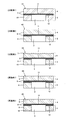
- FIG. 5 is a cross-sectional view schematically showing multilayer ceramic substrates 61 to 65 according to Comparative Examples 1 to 3 and Examples 1 and 2 manufactured in an experimental example carried out to confirm the effect of the present invention.
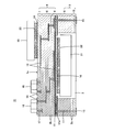
- FIG. 1 is a cross-sectional view showing a functional module 31 including a multilayer ceramic substrate 1 according to the first embodiment of the present invention.
- a cavity 3 is formed in the multilayer ceramic substrate 1.
- the multilayer ceramic substrate 1 has a bottom wall portion 4 that defines the bottom surface of the cavity 3 and a peripheral wall portion 5 that defines the peripheral surface of the cavity 3.
- the multilayer ceramic substrate 1 has a structure in which a plurality of first ceramic layers 2a having a through hole for forming a cavity and a plurality of second ceramic layers 2b having no through hole for forming a cavity are laminated.
- 5 is composed of the first ceramic layer 2a
- the bottom wall portion 4 is composed of the second ceramic layer 2b.
- the concave cavity 3 is formed in the multilayer ceramic substrate 1.
- the bottom wall portion 4 includes, as the second ceramic layer 2b, a first high thermal expansion coefficient layer 6 having a relatively high thermal expansion coefficient and first and second low thermal expansions having a relatively low thermal expansion coefficient.
- Coefficient layers 7 and 8 are arranged, and a laminated structure in which at least a part of the first high thermal expansion coefficient layer 6 is sandwiched between the first and second low thermal expansion coefficient layers 7 and 8 is formed.
- the outwardly facing surface of the bottom wall portion 4 is provided by the first low thermal expansion coefficient layer 7, and the surface of the bottom wall portion 4 in contact with the peripheral wall portion 5 is the second low thermal expansion coefficient layer. Is given by 8.
- a second high thermal expansion coefficient layer 9 having a higher thermal expansion coefficient than that of the second low thermal expansion coefficient layer 8 is disposed on the peripheral wall portion 5, and the outermost layer has a relative thermal expansion coefficient.
- a third low low thermal expansion coefficient layer 10 is disposed.
- first interlayer constraining layer 11 is disposed on the bottom wall portion 4 as the second ceramic layer 2b in a state of being in contact with the second low thermal expansion coefficient layer 8.
- first interlayer constraining layer 11 is sandwiched between the second low thermal expansion coefficient layers 8.
- the second interlayer constraining layer 12 is disposed along the surface of the peripheral wall portion 5 that is in contact with the bottom wall portion 4.
- the first interlayer constrained layer 11 may be disposed in a state sandwiched between the second low thermal expansion coefficient layer 8 and the first high thermal expansion coefficient layer 6.
- the multilayer ceramic substrate 1 includes various wiring conductors.
- the wiring conductor is used to form a passive element such as a capacitor or an inductor, or to perform connection wiring such as an electrical connection between elements, and is typically as shown in FIG. In addition, it is composed of several conductor films 13 to 16 and several via-hole conductors 17.
- the conductor film 13 is formed inside the multilayer ceramic substrate 1.
- Conductive films 14 and 15 are formed on one main surface and the other main surface of multilayer ceramic substrate 1, respectively.
- the conductor film 16 is formed on the bottom surface of the cavity 3.
- the via-hole conductor 17 is provided so as to penetrate any one of the ceramic layers 2a and 2b in the thickness direction while being electrically connected to any of the conductor films 13 to 16.
- Chip components 18 and 19 are mounted on one main surface of the multilayer ceramic substrate 1 in a state of being electrically connected to the external conductor film 14.
- FIG. 1 shows a bump electrode 20 for electrically connecting the chip component 19 to the external conductor film 14.
- FIG. 1 shows a bump electrode 22 for electrically connecting the chip component 21 to the cavity bottom conductor film 16.
- the functional module 31 is configured by mounting the chip components 18, 19 and 21 on the multilayer ceramic substrate 1.
- the external conductor film 15 formed on the other main surface of the multilayer ceramic substrate 1 is used as an electrical connection means when the functional module 31 is mounted on a mother board (not shown).
- the multilayer ceramic substrate 1 described above is manufactured, for example, as follows.
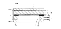
- FIG. 2 is a cross-sectional view showing a composite laminate 41 produced during the production of the multilayer ceramic substrate 1.
- the composite laminate 41 includes a raw laminate 42 to be the multilayer ceramic substrate 1 by firing, and first and second outer constraining layers 43 and 44 disposed on both main surfaces of the raw laminate 42. And.
- the conductor films 13 to 16 and the via-hole conductor 17 provided in association with the raw laminate 42 are not shown.
- the raw laminated body 42 includes a peripheral wall portion 4 that defines the bottom surface of the cavity 3 and a peripheral wall portion 5 that defines the peripheral surface of the cavity 3, as in the case of the multilayer ceramic substrate 1. And have.
- the bottom wall portion 4 of the raw laminate 42 has a first high thermal expansion coefficient green to be the first high thermal expansion coefficient layer 6 as the second ceramic green layer to be the second ceramic layer 2b.
- the first low thermal expansion coefficient green layer 47 to be the layer 46 and the first low thermal expansion coefficient layer 7 and the second low thermal expansion coefficient green layer 48 to be the second low thermal expansion coefficient layer 8 are laminated.
- the peripheral wall portion 5 of the raw laminate 42 has a second high thermal expansion coefficient green layer to be the second high thermal expansion coefficient layer 9 as the first ceramic green layer to be the first ceramic layer 2a. 49 and the third low thermal expansion coefficient green layer 50 to be the third low thermal expansion coefficient layer 10 are laminated.
- These green layers 46 to 50 contain a low-temperature sintered ceramic material.
- the first interlayer constraining layer 11 is formed as the second ceramic green layer
- the second interlayer constraining layer 12 is formed as the first ceramic green layer.
- These interlayer constrained layers 11 and 12 contain inorganic material powders that are not substantially sintered under firing conditions capable of sintering the above-described low-temperature sintered ceramic material.
- Each of the above-described green layers 46 to 50 is usually composed of a plurality of layers as can be seen from the fact that a plurality of ceramic layers 2a and a plurality of ceramic layers 2b are shown in FIG. In FIG. 2, illustration of the interface of these several layers is abbreviate
- Each of the outer constraining layers 43 and 44 may be composed of a plurality of layers.
- the raw laminate 42 is usually formed by laminating a plurality of ceramic green sheets, but instead, it may be formed by repeatedly applying ceramic slurry.
- the first and second outer constraining layers 43 and 44 are laminated on both main surfaces of the raw laminate 42, and the composite laminate 41 is obtained by pressure bonding.
- the second outer constraining layer 44 located on the cavity 3 side is provided with a through hole 51 communicating with the cavity 3.
- the composite laminate 41 is fired under the firing conditions in which the low-temperature sintered ceramic material described above is sintered.
- the inorganic material powder contained in the interlayer constraining layers 11 and 12 and the outer constraining layers 43 and 44 is not substantially sintered, the interlayer constraining layers 11 and 12 and the outer constraining layers 43 and 44 are substantially Contraction does not occur. Therefore, the shrinkage suppressing action by the interlayer constraining layers 11 and 12 and the outer constraining layers 43 and 44 is exerted on the raw laminate 42 until the sintered multilayer ceramic substrate 1 is obtained. As a result, undesired deformation such as warpage is less likely to occur in the obtained multilayer ceramic substrate 1, and the dimensional accuracy can be increased.
- the outer constraining layers 43 and 44 are removed from the fired composite laminate 41 by, for example, ultrasonic cleaning or blasting. Since the outer constraining layers 43 and 44 after firing are in a porous state, they can be easily pulverized and removed.
- the interlayer constrained layers 11 and 12 as a result of the firing process, the penetration of the material (glass component or the like) contained in the low thermal expansion coefficient green layer 48 and / or the high thermal expansion coefficient green layer 49 adjacent thereto.
- the inorganic material powder is solidified.
- the interlayer constraining layers 11 and 12 need to have a thickness that enables solidification by penetration of such materials.
- the multilayer ceramic substrate 1 is obtained as described above.
- the bottom wall portion 4 in the obtained multilayer ceramic substrate 1 there is a laminate in which at least a part of the first high thermal expansion coefficient layer 6 is sandwiched between the first and second low thermal expansion coefficient layers 7 and 8. A structure is formed. Therefore, compressive stress is generated in the first and second low thermal expansion coefficient layers 7 and 8 in the cooling process after the firing step, and as a result, the mechanical strength of the bottom wall portion 4 can be improved.
- the third low thermal expansion coefficient layer 10 is provided, and also here, compressive stress is generated in the cooling process after firing. Therefore, undesired deformation such as warpage due to the stress difference between the front and back surfaces of the multilayer ceramic substrate 1 can be suppressed.
- each thickness of the low thermal expansion coefficient layers 7, 8 and 10 is preferably 10 to 100 ⁇ m after firing. The reason is as follows.
- each of the low thermal expansion coefficient layers 7, 8 and 10 and each of the high thermal expansion coefficient layers 6 and 9 acts due to the difference in thermal expansion coefficient. More specifically, a compressive stress acts on the low thermal expansion coefficient layers 7, 8, and 10, and this compressive stress decreases as the distance from the interface increases. On the other hand, a tensile stress acts on the high thermal expansion coefficient layers 6 and 9, and this tensile stress decreases as the distance from the interface increases. This is because stress is relaxed as the distance from the interface increases. When the distance from the interface exceeds 100 ⁇ m, the compressive stress almost does not act and the effect is hardly seen. Therefore, the thickness of each of the low thermal expansion coefficient layers 7, 8 and 10 is preferably 100 ⁇ m or less.
- each of the low thermal expansion coefficient layers 7, 8 and 10 when the thickness of each of the low thermal expansion coefficient layers 7, 8 and 10 is less than 10 ⁇ m, the high thermal expansion coefficient layers 6 and 9, whose strength has been reduced due to the acting tensile stress, It exists in the outer surface vicinity area
- Each of the low thermal expansion coefficient layers 7, 8 and 10 preferably has a thickness of 10 ⁇ m or more.
- the thicknesses of the high thermal expansion coefficient layers 6 and 9 are appropriately determined according to the total thickness of the multilayer ceramic substrate 1 and the thicknesses of the low thermal expansion coefficient layers 7, 8 and 10, but are 10 to 100 ⁇ m after firing. It is preferable.
- the thickness of the first and second low thermal expansion coefficient layers 7 and 8 sandwiching the first high thermal expansion coefficient layer 6 is such that the thinner the thickness of the first high thermal expansion coefficient layer 6 is, the more efficiently the compressive stress is used. This is preferable because it can be performed.
- the thicknesses of the second and third low thermal expansion coefficient layers 8 and 10 sandwiching the second high thermal expansion coefficient layer 9 are preferably thinner than the thickness of the second high thermal expansion coefficient layer 9.
- the first to third low thermal expansion coefficient layers 7, 8, and 10 are shown to have the same thickness, but the balance between the bottom wall portion 4 and the peripheral wall portion 5, the cavity These thicknesses may be made different from each other in accordance with the design of the multilayer ceramic substrate 1 such as the size of the diameter of 3.
- the low thermal expansion coefficient layer 7 is illustrated as being composed of three ceramic layers 2b.
- the thickness of the low thermal expansion coefficient layer 7 is one layer of the ceramic layer 2b. It is not the thickness of the minute but the total thickness of the three ceramic layers 2b. The same applies to the thicknesses of the other low thermal expansion coefficient layers 8 and 10 and the thicknesses of the high thermal expansion coefficient layers 6 and 9.
- the difference in thermal expansion coefficient between the low thermal expansion coefficient layers 7, 8 and 10 and the high thermal expansion coefficient layers 6 and 9 is preferably 1.0 ppmK ⁇ 1 or more and 4.3 ppmK ⁇ 1 or less.
- the warp of the bottom wall portion 4 can be greatly reduced by setting the difference in thermal expansion coefficient to 1.0 ppm K ⁇ 1 or more. That is, the relationship between the amount of warpage and the difference in thermal expansion coefficient is as follows. In the region where the difference in thermal expansion coefficient is less than 1.0 ppmK ⁇ 1 , the amount of warpage decreases as the difference in thermal expansion coefficient increases, and at 1.0 ppmK ⁇ 1 or more, It was found to be almost constant.
- the in-plane stress that acts to warp the multilayer ceramic substrate 1 is relatively smaller than the stress that acts in the in-plane direction on the front and back surfaces due to the difference in thermal expansion coefficient. It is presumed that.
- SiO 2 contained in the glass contained in the material constituting the low thermal expansion coefficient coefficient layers 7, 8 and 10 is 34 to 73 wt%, and is contained in the material constituting the high thermal expansion coefficient coefficient layers 6 and 9. SiO 2 contained in the glass is 22 to 60% by weight.
- the preferable composition and the content thereof as described above are obtained by using a borosilicate glass-based material to reduce the difference in thermal expansion coefficient between the low thermal expansion coefficient coefficient layers 7, 8 and 10 and the high thermal expansion coefficient coefficient layers 6 and 9 by 1.
- 0.0 ppm K ⁇ 1 or more is suitable and the weight ratio of common components is suitable to be 75% by weight or more.
- a sufficient bonding force is obtained between each of the low thermal expansion coefficient coefficient layers 7, 8 and 10 and each of the high thermal expansion coefficient coefficient layers 6 and 9 by setting the weight ratio of the common components to 75% by weight or more. Can do.
- the SiO 2 component contained in the glass contributes to lowering the thermal expansion coefficient, and the MO component contributes to raising the thermal expansion coefficient.
- the glass composition is preferably close to the precipitated crystal composition.
- the glass composition is preferably close to the precipitated crystal composition.
- crystals of MAl 2 Si 2 O 8 and MSiO 3 are likely to precipitate, so that SiO 2 is close to this crystal composition. It is preferable to adjust the ratio of MO to MO.
- the glass composition of the low thermal expansion coefficient coefficient layer 7, 8 and 10 for decreasing the thermal expansion coefficient the ratio of SiO 2 to MO is well closer to 2
- the ratio between SiO 2 and MO is preferably close to 1 in order to increase the thermal expansion coefficient.
- the glass composition of the high thermal expansion coefficient coefficient layers 6 and 9 has a higher MO ratio than the low thermal expansion coefficient coefficient layers 7, 8 and 10, and is susceptible to erosion in the plating process after firing, but is exposed to the surface portion. Because it is not, it has a structure that is less susceptible to fatal damage.
- the ratio of SiO 2 and MO in the glass can be selected in the ranges as described above for the low thermal expansion coefficient coefficient layers 7, 8 and 10 and the high thermal expansion coefficient coefficient layers 6 and 9, respectively. preferable.
- the glass contained in the material constituting the low coefficient of thermal expansion coefficient layers 7, 8 and 10 is composed of 34 to 73 wt% SiO 2 , 14 to 41 wt% MO, 0 to 30 wt% B 2 O 3 , 0-30 wt% Al 2 O 3, and the glass included in the material constituting the high coefficient of thermal expansion coefficient layers 6 and 9 has 22-60 wt% SiO 2 and 22-60 wt% MO. And 0 to 20 wt% B 2 O 3 and 0 to 30 wt% Al 2 O 3 are more preferable. The reason is as follows.
- B 2 O 3 imparts an appropriate viscosity to the glass so that sintering proceeds smoothly during firing.
- B 2 O 3 is too large, the viscosity is too low, becomes excessive sintering, pores on the surface becomes poor insulation occurs.
- B 2 O 3 is too small, high viscosity, a sintering defect.
- Al 2 O 3 is a component constituting the precipitated crystal. Even if the Al 2 O 3 is too much or too little, crystal precipitation hardly occurs.
- the material constituting the low thermal expansion coefficient coefficient layers 7, 8 and 10 contains 30 to 60% by weight of Al 2 O 3 as a filler, and the material constituting the high thermal expansion coefficient coefficient layers 6 and 9 is Al 2 as a filler. More preferably, it contains 40 to 70% by weight of O 3 . The reason is as follows.
- the Al 2 O 3 filler contributes to improving the mechanical strength. If there is too little Al 2 O 3 filler, sufficient strength cannot be obtained. In particular, in the high thermal expansion coefficient coefficient layers 6 and 9 on which tensile stress is applied, if the mechanical strength is not sufficient, the high thermal expansion coefficient coefficient layers 6 and 9 are broken from the high thermal expansion coefficient coefficient layers 6 and 9. The effect of strengthening 10 cannot be obtained sufficiently. For this reason, the high thermal expansion coefficient coefficient layers 6 and 9 contain more Al 2 O 3 filler than the low thermal expansion coefficient layers 7, 8 and 10, and by increasing the strength, it is possible to increase the difference in thermal expansion coefficient. In addition, the effect of strengthening the low coefficient of thermal expansion coefficient layers 7, 8 and 10 can be obtained.
- the Al 2 O 3 filler Since the Al 2 O 3 filler has an intermediate contribution to the thermal expansion coefficient between the glass in the low thermal expansion coefficient coefficient layers 7, 8 and 10 and the glass in the high thermal expansion coefficient layer 6 and 9, If there is too much Al 2 O 3 filler, the difference in thermal expansion coefficient cannot be obtained.
- the first to third low thermal expansion coefficient layers 7, 8, and 10 do not have to have the same composition and have the same thermal expansion coefficient, and the first and second high thermal expansion coefficients.
- the layers 6 and 10 need not have the same composition and the same thermal expansion coefficient.
- the thermal expansion coefficient of each of the first and second low thermal expansion coefficient layers 7 and 8 is smaller than the thermal expansion coefficient of the first high thermal expansion coefficient layer 6, the thermal expansion coefficient of the first low thermal expansion coefficient layer 7.
- the thermal expansion coefficient of the second low thermal expansion coefficient layer 8 may be different from each other.
- the thermal expansion coefficient of each of the second and third low thermal expansion coefficient layers 8 and 10 is smaller than the thermal expansion coefficient of the second high thermal expansion coefficient layer 9, the thermal expansion coefficient of the second low thermal expansion coefficient layer 8 will be described.
- the thermal expansion coefficient of the third low thermal expansion coefficient layer 10 may be different from each other. Therefore, as long as the above conditions are satisfied, each coefficient of thermal expansion can be freely set, and as a result, the degree of freedom in designing the cavity 3 can be improved.
- FIGS. 3 and 4 are for explaining a second embodiment of the present invention, and correspond to FIGS. 1 and 2, respectively. 3 and 4, elements corresponding to those shown in FIGS. 1 and 2 are denoted by the same reference numerals, and redundant description is omitted.
- the inner peripheral edge defining the through hole for forming a cavity of the second interlayer constraining layer 12a is the second interlayer constraining of the peripheral wall portion 5.
- the first ceramic layer 2a in contact with the layer 12a is located on the inner side of the inner peripheral edge defining the cavity forming through hole.
- first cavity forming through-hole all of the inner peripheral edge defining the cavity forming through-hole (hereinafter referred to as “first cavity forming through-hole”) of the second interlayer constraining layer 12a is formed in the second interlayer constraining layer 12a. It is not always necessary that the first ceramic layer 2a in contact with the first ceramic layer 2a is located on the inner side of the inner peripheral edge defining the cavity forming through hole (hereinafter referred to as "second cavity forming through hole”). . That is, it is only necessary that at least a part of the inner peripheral edge defining the first cavity forming through hole is located inside the inner peripheral edge defining the second cavity forming through hole.
- the inner peripheral edge that defines the first cavity forming through hole is not located outside the inner peripheral edge that defines the second cavity forming through hole.
- a part of the inner peripheral edge that defines the first cavity forming through hole is at least the second edge even if it is not located inside the inner peripheral edge that defines the second cavity forming through hole. It must be in the same position as the inner peripheral edge that defines the cavity forming through hole.
- the inner peripheral edge defining the first cavity forming through-hole is the other two sides of the quadrangle, That is, it should not be outside the inner peripheral edge defining the second cavity forming through hole, and at least be in the same position.
- the first cavity forming through-hole is made smaller, so that at least a part of the inner peripheral edge defining the first cavity forming through hole is smaller than the inner peripheral edge defining the second cavity forming through hole. Also be positioned inside.
- a green sheet laminating step is performed.
- the second layer is undesirably performed.
- the inner peripheral edge defining the first cavity forming through hole is the second cavity.
- At least a part of the inner peripheral edge defining the first cavity forming through-hole is not located outside the inner peripheral edge defining the forming through-hole, and the inner peripheral edge defining the second cavity forming through-hole.
- FIG. 5 is a sectional view showing a multilayer ceramic substrate 1a according to the third embodiment of the present invention.
- the multilayer ceramic substrate 1b is illustrated in a simplified manner as compared with FIG. 1, but the elements corresponding to the elements illustrated in FIG. .
- the multilayer ceramic substrate 1b shown in FIG. 5 is characterized by not including an interlayer constraining layer.
- the other configuration may be understood to be the same as that of the multilayer ceramic substrate 1 shown in FIG. 1 or the multilayer ceramic substrate 1a shown in FIG.
- the multilayer ceramic substrate 1, 1a or 1b may not include the third low thermal expansion coefficient layer 10.
- the multilayer ceramic substrate 65 according to Example 2 has the configuration of the multilayer ceramic substrate 1 shown in FIG.
- the ceramic layers constituting the bottom wall portion 4 are all provided by the low thermal expansion coefficient layer 7.
- All the ceramic layers constituting the peripheral wall portion 5 are provided by the low thermal expansion coefficient layer 10.
- the ceramic layers constituting the peripheral wall portion 4 are all provided by the high thermal expansion coefficient layer 6, and the ceramic layers constituting the peripheral wall portion 5 are all provided by the high thermal expansion coefficient layer 9. It is characterized by.
- the multilayer ceramic substrate 63 according to Comparative Example 3 is characterized in that the bottom wall portion 4 does not include the second low thermal expansion coefficient layer 8 and the high thermal expansion coefficient layer 6 is formed in this portion.
- the multilayer ceramic substrate 64 according to the first embodiment is characterized in that the third low thermal expansion coefficient layer 10 is not provided and the high thermal expansion coefficient layer 9 is formed up to this portion.
- the thermal expansion coefficients of the low thermal expansion coefficient layers 7, 8 and 10 were set to 5.3 ppmK ⁇ 1 . Further, in order to form the low thermal expansion coefficient layers 7, 8 and 10, a green sheet having a thickness of 50 ⁇ m was prepared, and an appropriate number of green sheets were laminated so as to have a desired thickness as described later.
- the green sheets for the low coefficient of thermal expansion layers 7, 8 and 10 contain borosilicate glass powder and ceramic powder in a weight ratio of 60:40, and the total amount of glass powder and ceramic powder is 100 parts by weight.
- 50 parts by weight of an organic solvent, 10 parts by weight of a butyral binder and 1 part by weight of a plasticizer were added and mixed to form a slurry. After removing bubbles from the slurry, the slurry was formed into a sheet by a doctor blade method. And obtained by drying.
- the borosilicate glass powder includes 46 wt% SiO 2 , 30 wt% B 2 O 3 , 14 wt% CaO, 5 wt% Al 2 O 3 and 5 wt% TiO 2. Al 2 O 3 powder was used as the ceramic powder.
- the thermal expansion coefficients of the high thermal expansion coefficient layers 6 and 9 were set to 7.7 ppmK- 1 . Further, in order to form the high thermal expansion coefficient layers 6 and 9, a green sheet having a thickness of 50 ⁇ m was prepared, and an appropriate number of green sheets were laminated so as to have a desired thickness as described later.
- High thermal expansion coefficient layers 6 and 9 The green sheets for the high thermal expansion coefficient layers 6 and 9 contain borosilicate glass powder and ceramic powder in a weight ratio of 70:30. An organic solvent, a butyral binder and a plasticizer were added in the same ratio as in the case of the low thermal expansion coefficient layer described above with respect to a total of 100 parts by weight, and the same operation was performed.
- the borosilicate glass powder used those containing 40 wt% of SiO 2, 5 wt% of B 2 O 3, 40 wt% of CaO, 5 wt% of MgO and 10% by weight of Al 2 O 3
- the ceramic powder Al 2 O 3 powder was used.
- a green sheet having a thickness of 10 ⁇ m was prepared in order to form the interlayer constraining layers 11 and 12, and a green sheet having a thickness of 100 ⁇ m was prepared in order to form an outer constraining layer (not shown in FIG. 6).
- the green sheets for the interlayer constraining layers 11 and 12 and the outer constraining layer include 100 parts by weight of alumina powder, 10 parts by weight of a butyral binder, and 1 part by weight of a plasticizer. It was obtained through the same operation as in.
- a paste containing 48 parts by weight of silver powder, 3 parts by weight of ethylcellulose binder and 49 parts by weight of organic solvent terpenes is used.
- this conductive paste was applied to a specific one of the above green sheets.
- various green sheets are laminated in a number as shown in “Number of used green sheets” in Table 1 below to produce raw laminates to be the multilayer ceramic substrates 61 to 65, respectively.
- a composite laminate was produced by forming outer constraining layers on the top and bottom.
- the outer constraining layer was formed by laminating four green sheets each having a thickness of 100 ⁇ m for the outer constraining layer above and below the raw laminate.
- the composite laminate was baked under the condition of holding at a temperature of 870 ° C. for 10 minutes.
- the outer constraining layer adhering in a porous state to the surface of the fired composite laminate is removed using an ultrasonic cleaner, and the multilayers according to Comparative Examples 1 to 3 and Examples 1 and 2 are used. Ceramic substrates 61 to 65 were obtained.
- Each of the multilayer ceramic substrates 61 to 65 was mounted on a mounting substrate using solder, the mounting substrate was attached to the inside of a rectangular parallelepiped housing, and dropped toward the concrete block. At this time, dropping each of the six surfaces of the casing sequentially downward was regarded as one cycle, and this test was performed up to 10 cycles. In each bottom wall 4 of each of the multilayer ceramic substrates 61 to 64, the number of cycles at which breakage or crack generation occurred was evaluated. The results are shown in Table 2.
Landscapes
- Engineering & Computer Science (AREA)
- Microelectronics & Electronic Packaging (AREA)
- Physics & Mathematics (AREA)
- Ceramic Engineering (AREA)
- Chemical & Material Sciences (AREA)
- Power Engineering (AREA)
- Computer Hardware Design (AREA)
- General Physics & Mathematics (AREA)
- Condensed Matter Physics & Semiconductors (AREA)
- Manufacturing & Machinery (AREA)
- Thermal Sciences (AREA)
- Inorganic Chemistry (AREA)
- Structural Engineering (AREA)
- Mechanical Engineering (AREA)
- Production Of Multi-Layered Print Wiring Board (AREA)
Abstract
Description


2a,2b セラミック層
3 キャビティ
4 底壁部
5 周壁部
6 第1の高熱膨張係数層
7 第1の低熱膨張係数層
8 第2の低熱膨張係数層
9 第2の高熱膨張係数層
10 第3の低熱膨張係数層
11 第1の層間拘束層
12,12a 第2の層間拘束層
41,41a 複合積層体
42 生の積層体
43,44 外側拘束層
46 第1の高熱膨張係数グリーン層
47 第1の低熱膨張係数グリーン層
48 第2の低熱膨張係数グリーン層
49 第2の高熱膨張係数グリーン層
50 第3の低熱膨張係数グリーン層
Claims (10)
- キャビティ形成用貫通孔を有する第1のセラミック層からなる周壁部と、前記キャビティ形成用貫通孔を有しない第2のセラミック層からなる底壁部とを有する、キャビティ付きの、多層セラミック基板であって、
前記底壁部には、前記第2のセラミック層として、熱膨張係数が相対的に高い高熱膨張係数層および熱膨張係数が相対的に低い低熱膨張係数層を含む、少なくとも2種類のセラミック層が配置され、かつ前記高熱膨張係数層の少なくとも一部が第1および第2の前記低熱膨張係数層に挟まれる積層構造が形成されている、多層セラミック基板。 - 前記底壁部の外方に向く面が前記第1の低熱膨張係数層によって与えられ、前記底壁部の、前記周壁部と接する面が前記第2の低熱膨張係数層によって与えられる、請求項1に記載の多層セラミック基板。
- 前記周壁部には、前記第2の低熱膨張係数層より高い熱膨張係数を有する高熱膨張係数層が配置されるとともに、その最外層には、熱膨張係数が相対的に低い第3の低熱膨張係数層が配置されている、請求項2に記載の多層セラミック基板。
- 前記底壁部は、前記第2のセラミック層として、前記第2の低熱膨張係数層に接触する状態で配置される第1の層間拘束層をさらに備え、前記第1の層間拘束層は、前記低熱膨張係数層に含まれるセラミック材料を焼結させ得る焼成条件では実質的に焼結しない無機材料粉末を含みかつ前記低熱膨張係数層に含まれていた材料の浸透によって前記無機材料粉末が固化された状態にある、請求項2または3に記載の多層セラミック基板。
- 前記周壁部は、前記第1のセラミック層として、当該周壁部の、前記底壁部と接する面に沿って配置される第2の層間拘束層をさらに備え、前記第2の層間拘束層は、前記低熱膨張係数層に含まれるセラミック材料を焼結させ得る焼成条件では実質的に焼結しない無機材料粉末を含みかつ前記低熱膨張係数層に含まれていた材料の浸透によって前記無機材料粉末が固化された状態にある、請求項1ないし4のいずれかに記載の多層セラミック基板。
- 前記第2の層間拘束層が有する前記キャビティ形成用貫通孔を規定する内周縁は、前記周壁部の、前記第2の層間拘束層に接する前記第1のセラミック層が有する前記キャビティ形成用貫通孔を規定する内周縁よりも外側に位置せず、かつ、その少なくとも一部は、前記周壁部の、前記第2の層間拘束層に接する前記第1のセラミック層が有する前記キャビティ形成用貫通孔を規定する内周縁よりも内側に位置している、請求項5に記載の多層セラミック基板。
- キャビティ形成用貫通孔を有する第1のセラミック層からなる周壁部と、前記キャビティ形成用貫通孔を有しない第2のセラミック層からなる底壁部とを有し、前記底壁部には、前記第2のセラミック層として、熱膨張係数が相対的に高い高熱膨張係数層および熱膨張係数が相対的に低い低熱膨張係数層を含む、少なくとも2種類のセラミック層が配置され、かつ前記高熱膨張係数層の少なくとも一部が第1および第2の前記低熱膨張係数層に挟まれる積層構造が形成されている、キャビティ付きの、多層セラミック基板を製造する方法であって、
焼成することによって前記第1のセラミック層となるべきものであり、低温焼結セラミック材料を含み、前記キャビティ形成用貫通孔を有する第1のセラミックグリーン層を準備する工程と、
焼成することによって前記第2のセラミック層となるべき第2のセラミックグリーン層として、それぞれ低温焼結セラミック材料を含む、前記高熱膨張係数層となるべき高熱膨張係数グリーン層と前記第1の低熱膨張係数層となるべき第1の低熱膨張係数グリーン層と前記第2の低熱膨張係数層となるべき第2の低熱膨張係数グリーン層とを準備する工程と、
前記第1のセラミックグリーン層と前記第2のセラミックグリーン層とを積層してなる、生の積層体と、前記生の積層体の両主面上に配置され、前記低温焼結セラミック材料を焼結させ得る焼成条件では実質的に焼結しない無機材料粉末を含む、外側拘束層とを備える、複合積層体を作製する工程と、
前記複合積層体を前記低温焼結セラミック材料が焼結する焼成条件で焼成する焼成工程と、
次いで、前記複合積層体から前記外側拘束層を除去する工程と
を備える、多層セラミック基板の製造方法。 - 前記多層セラミック基板において、前記底壁部の外方に向く面が前記第1の低熱膨張係数層によって与えられ、前記底壁部の前記周壁部と接する面が前記第2の低熱膨張係数層によって与えられ、前記生の積層体は、前記第2のセラミックグリーン層として、前記第2の低熱膨張係数グリーン層に接触する状態で配置される第1の層間拘束層をさらに備え、前記第1の層間拘束層は、前記低温焼結セラミック材料を焼結させ得る焼成条件では実質的に焼結しない無機材料粉末を含み、前記焼成工程の結果、前記低熱膨張係数グリーン層に含まれていた材料の浸透によって前記無機材料粉末が固化された状態になる、請求項7に記載の多層セラミック基板の製造方法。
- 前記生の積層体は、前記第1のセラミックグリーン層として、前記多層セラミック基板における前記周壁部の、前記底壁部と接する面に沿って配置される第2の層間拘束層をさらに備え、前記第2の層間拘束層は、前記低熱膨張係数層に含まれるセラミック材料を焼結させ得る焼成条件では実質的に焼結しない無機材料粉末を含み、前記焼成工程の結果、前記低熱膨張係数層に含まれていた材料の浸透によって前記無機材料粉末が固化された状態になる、請求項7または8に記載の多層セラミック基板の製造方法。
- 前記生の積層体において、前記第2の層間拘束層が有する前記キャビティ形成用貫通孔は、前記周壁部の、前記第2の層間拘束層に接する前記第1のセラミックグリーン層が有する前記キャビティ形成用貫通孔よりも小さくされる、請求項9に記載の多層セラミック基板の製造方法。
Priority Applications (4)
| Application Number | Priority Date | Filing Date | Title |
|---|---|---|---|
| CN200980117809XA CN102027813A (zh) | 2008-05-15 | 2009-04-21 | 多层陶瓷基板及其制造方法 |
| JP2010511935A JP5182367B2 (ja) | 2008-05-15 | 2009-04-21 | 多層セラミック基板およびその製造方法 |
| US12/940,073 US8993105B2 (en) | 2008-05-15 | 2010-11-05 | Multilayer ceramic substrate and method for producing the same |
| US14/465,876 US20140361470A1 (en) | 2008-05-15 | 2014-08-22 | Multilayer ceramic substrate and method for producing the same |
Applications Claiming Priority (4)
| Application Number | Priority Date | Filing Date | Title |
|---|---|---|---|
| JP2008128102 | 2008-05-15 | ||
| JP2008-128102 | 2008-05-15 | ||
| JP2008332086 | 2008-12-26 | ||
| JP2008-332086 | 2008-12-26 |
Related Child Applications (1)
| Application Number | Title | Priority Date | Filing Date |
|---|---|---|---|
| US12/940,073 Continuation US8993105B2 (en) | 2008-05-15 | 2010-11-05 | Multilayer ceramic substrate and method for producing the same |
Publications (1)
| Publication Number | Publication Date |
|---|---|
| WO2009139272A1 true WO2009139272A1 (ja) | 2009-11-19 |
Family
ID=41318645
Family Applications (1)
| Application Number | Title | Priority Date | Filing Date |
|---|---|---|---|
| PCT/JP2009/057896 WO2009139272A1 (ja) | 2008-05-15 | 2009-04-21 | 多層セラミック基板およびその製造方法 |
Country Status (4)
| Country | Link |
|---|---|
| US (2) | US8993105B2 (ja) |
| JP (1) | JP5182367B2 (ja) |
| CN (2) | CN104589738A (ja) |
| WO (1) | WO2009139272A1 (ja) |
Cited By (2)
| Publication number | Priority date | Publication date | Assignee | Title |
|---|---|---|---|---|
| JP2019071420A (ja) * | 2013-08-26 | 2019-05-09 | 日立金属株式会社 | 実装基板用ウエハ、多層セラミックス基板、実装基板、チップモジュール、及び実装基板用ウエハの製造方法 |
| JP2020193896A (ja) * | 2019-05-29 | 2020-12-03 | 日本特殊陶業株式会社 | 電気検査用基板 |
Families Citing this family (7)
| Publication number | Priority date | Publication date | Assignee | Title |
|---|---|---|---|---|
| JP5846187B2 (ja) * | 2013-12-05 | 2016-01-20 | 株式会社村田製作所 | 部品内蔵モジュール |
| US20150289365A1 (en) * | 2014-04-08 | 2015-10-08 | Apple Inc. | Circuit Carrier With Interior Plating Lines and Peripheral Shielding |
| US20180277395A1 (en) * | 2015-10-09 | 2018-09-27 | Hitachi Metals ,Ltd. | Method for manufacturing multilayer ceramic substrate |
| FR3042647B1 (fr) * | 2015-10-20 | 2017-12-01 | Soitec Silicon On Insulator | Structure composite et procede de fabrication associe |
| CN114208402A (zh) * | 2019-08-06 | 2022-03-18 | 日本电气硝子株式会社 | 陶瓷布线基板、陶瓷布线基板用陶瓷生片以及陶瓷布线基板用玻璃陶瓷粉末 |
| CN111892350B (zh) * | 2020-07-03 | 2022-04-15 | 大连大学 | 一种提升水泥砂浆、混凝土抗折强度的方法 |
| CN112321163B (zh) * | 2020-10-28 | 2021-06-15 | 中国科学院上海硅酸盐研究所 | 一种高强度ltcc基板材料及其制备方法 |
Citations (5)
| Publication number | Priority date | Publication date | Assignee | Title |
|---|---|---|---|---|
| JPH0629664A (ja) * | 1992-07-10 | 1994-02-04 | Nippon Cement Co Ltd | 多層セラミックス配線基板 |
| JP2004095767A (ja) * | 2002-08-30 | 2004-03-25 | Murata Mfg Co Ltd | セラミック多層基板およびその製造方法 |
| JP2007067364A (ja) * | 2004-09-03 | 2007-03-15 | Murata Mfg Co Ltd | チップ型電子部品を搭載したセラミック基板及びその製造方法 |
| JP2007073728A (ja) * | 2005-09-07 | 2007-03-22 | Murata Mfg Co Ltd | 多層セラミック基板およびその製造方法ならびに電子部品 |
| JP2008030995A (ja) * | 2006-07-28 | 2008-02-14 | Murata Mfg Co Ltd | 多層セラミック基板およびその製造方法ならびに多層セラミック基板作製用複合グリーンシート |
Family Cites Families (13)
| Publication number | Priority date | Publication date | Assignee | Title |
|---|---|---|---|---|
| JP3656484B2 (ja) * | 1999-03-03 | 2005-06-08 | 株式会社村田製作所 | セラミック多層基板の製造方法 |
| JP2001230548A (ja) * | 2000-02-21 | 2001-08-24 | Murata Mfg Co Ltd | 多層セラミック基板の製造方法 |
| US6809413B1 (en) * | 2000-05-16 | 2004-10-26 | Sandia Corporation | Microelectronic device package with an integral window mounted in a recessed lip |
| JP3757788B2 (ja) * | 2000-11-27 | 2006-03-22 | 株式会社村田製作所 | 多層セラミック基板およびその製造方法 |
| JP4748435B2 (ja) * | 2001-08-21 | 2011-08-17 | 日本電気硝子株式会社 | 積層ガラスセラミック材料及び積層ガラスセラミック焼結体 |
| JP2003273513A (ja) | 2002-03-14 | 2003-09-26 | Murata Mfg Co Ltd | キャビティ付き多層セラミック基板の製造方法およびキャビティ付き多層セラミック基板 |
| JP3972957B2 (ja) | 2004-09-03 | 2007-09-05 | 株式会社村田製作所 | チップ型電子部品を搭載したセラミック基板の製造方法 |
| JP4557002B2 (ja) * | 2005-07-01 | 2010-10-06 | 株式会社村田製作所 | 多層セラミック基板およびその製造方法ならびに多層セラミック基板作製用複合グリーンシート |
| JP4994052B2 (ja) * | 2006-03-28 | 2012-08-08 | 京セラ株式会社 | 基板およびこれを用いた回路基板 |
| WO2007142112A1 (ja) * | 2006-06-02 | 2007-12-13 | Murata Manufacturing Co., Ltd. | 多層セラミック基板およびその製造方法ならびに電子部品 |
| JP5104761B2 (ja) * | 2007-04-09 | 2012-12-19 | 株式会社村田製作所 | セラミック基板およびその製造方法 |
| JP4821855B2 (ja) * | 2007-04-11 | 2011-11-24 | 株式会社村田製作所 | 多層セラミック基板およびその製造方法 |
| WO2009069398A1 (ja) * | 2007-11-30 | 2009-06-04 | Murata Manufacturing Co., Ltd. | セラミック複合多層基板及びその製造方法並びに電子部品 |
-
2009
- 2009-04-21 JP JP2010511935A patent/JP5182367B2/ja not_active Expired - Fee Related
- 2009-04-21 CN CN201410815104.8A patent/CN104589738A/zh active Pending
- 2009-04-21 WO PCT/JP2009/057896 patent/WO2009139272A1/ja active Application Filing
- 2009-04-21 CN CN200980117809XA patent/CN102027813A/zh active Pending
-
2010
- 2010-11-05 US US12/940,073 patent/US8993105B2/en not_active Expired - Fee Related
-
2014
- 2014-08-22 US US14/465,876 patent/US20140361470A1/en not_active Abandoned
Patent Citations (5)
| Publication number | Priority date | Publication date | Assignee | Title |
|---|---|---|---|---|
| JPH0629664A (ja) * | 1992-07-10 | 1994-02-04 | Nippon Cement Co Ltd | 多層セラミックス配線基板 |
| JP2004095767A (ja) * | 2002-08-30 | 2004-03-25 | Murata Mfg Co Ltd | セラミック多層基板およびその製造方法 |
| JP2007067364A (ja) * | 2004-09-03 | 2007-03-15 | Murata Mfg Co Ltd | チップ型電子部品を搭載したセラミック基板及びその製造方法 |
| JP2007073728A (ja) * | 2005-09-07 | 2007-03-22 | Murata Mfg Co Ltd | 多層セラミック基板およびその製造方法ならびに電子部品 |
| JP2008030995A (ja) * | 2006-07-28 | 2008-02-14 | Murata Mfg Co Ltd | 多層セラミック基板およびその製造方法ならびに多層セラミック基板作製用複合グリーンシート |
Cited By (3)
| Publication number | Priority date | Publication date | Assignee | Title |
|---|---|---|---|---|
| JP2019071420A (ja) * | 2013-08-26 | 2019-05-09 | 日立金属株式会社 | 実装基板用ウエハ、多層セラミックス基板、実装基板、チップモジュール、及び実装基板用ウエハの製造方法 |
| JP2020193896A (ja) * | 2019-05-29 | 2020-12-03 | 日本特殊陶業株式会社 | 電気検査用基板 |
| JP7296784B2 (ja) | 2019-05-29 | 2023-06-23 | 日本特殊陶業株式会社 | 電気検査用基板 |
Also Published As
| Publication number | Publication date |
|---|---|
| CN102027813A (zh) | 2011-04-20 |
| US20140361470A1 (en) | 2014-12-11 |
| JP5182367B2 (ja) | 2013-04-17 |
| US8993105B2 (en) | 2015-03-31 |
| CN104589738A (zh) | 2015-05-06 |
| US20110045242A1 (en) | 2011-02-24 |
| JPWO2009139272A1 (ja) | 2011-09-15 |
Similar Documents
| Publication | Publication Date | Title |
|---|---|---|
| JP5182367B2 (ja) | 多層セラミック基板およびその製造方法 | |
| JP4957723B2 (ja) | 多層セラミック基板およびその製造方法ならびに電子部品 | |
| JP4793447B2 (ja) | 多層セラミック基板およびその製造方法ならびに電子部品 | |
| JP5029699B2 (ja) | セラミック複合多層基板及びその製造方法並びに電子部品 | |
| JP2001358247A (ja) | 多層配線基板の製造方法 | |
| JP4613878B2 (ja) | 積層基板及びその製造方法 | |
| JP2011040604A (ja) | 積層型セラミック電子部品およびその製造方法 | |
| JP4788544B2 (ja) | 多層セラミック基板およびその製造方法 | |
| JP2012227310A (ja) | セラミックス多層基板とその製造方法 | |
| JP4826356B2 (ja) | セラミック基板の製造方法 | |
| JP4497247B2 (ja) | 積層型セラミック電子部品の製造方法 | |
| CN110024498B (zh) | 多层陶瓷基板以及电子装置 | |
| JP4028810B2 (ja) | 多層配線基板の製造方法 | |
| WO2009151006A1 (ja) | セラミック成形体の製造方法 | |
| JP5354011B2 (ja) | 多層セラミック基板の製造方法 | |
| JP4089356B2 (ja) | 多層セラミック基板の製造方法 | |
| US20130266782A1 (en) | Metal base substrate | |
| WO2010007878A1 (ja) | 多層セラミック基板およびその製造方法 | |
| JP2008159726A (ja) | 多層配線基板 | |
| JP6336841B2 (ja) | 配線基板 | |
| JP2005216931A (ja) | 樹脂フィルム付き金属箔、樹脂フィルム付き配線ユニット及び配線基板並びにその製造方法。 | |
| JP2006135195A (ja) | セラミック多層基板の製造方法、並びにこの製造方法に用いられるセラミックグリーンシート | |
| JP2007266353A (ja) | 多層セラミックス基板の製造方法 | |
| JP2006181738A (ja) | セラミック積層体 | |
| JP2008186907A (ja) | 多層回路基板の製造方法 |
Legal Events
| Date | Code | Title | Description |
|---|---|---|---|
| WWE | Wipo information: entry into national phase |
Ref document number: 200980117809.X Country of ref document: CN |
|
| 121 | Ep: the epo has been informed by wipo that ep was designated in this application |
Ref document number: 09746479 Country of ref document: EP Kind code of ref document: A1 |
|
| WWE | Wipo information: entry into national phase |
Ref document number: 2010511935 Country of ref document: JP |
|
| NENP | Non-entry into the national phase |
Ref country code: DE |
|
| 122 | Ep: pct application non-entry in european phase |
Ref document number: 09746479 Country of ref document: EP Kind code of ref document: A1 |