WO2009128416A1 - 光学表示装置製造システム及び光学表示装置製造方法 - Google Patents
光学表示装置製造システム及び光学表示装置製造方法 Download PDFInfo
- Publication number
- WO2009128416A1 WO2009128416A1 PCT/JP2009/057430 JP2009057430W WO2009128416A1 WO 2009128416 A1 WO2009128416 A1 WO 2009128416A1 JP 2009057430 W JP2009057430 W JP 2009057430W WO 2009128416 A1 WO2009128416 A1 WO 2009128416A1
- Authority
- WO
- WIPO (PCT)
- Prior art keywords
- optical film
- liquid crystal
- crystal cell
- film
- optical
- Prior art date
Links
Images


Classifications
-
- G—PHYSICS
- G02—OPTICS
- G02F—OPTICAL DEVICES OR ARRANGEMENTS FOR THE CONTROL OF LIGHT BY MODIFICATION OF THE OPTICAL PROPERTIES OF THE MEDIA OF THE ELEMENTS INVOLVED THEREIN; NON-LINEAR OPTICS; FREQUENCY-CHANGING OF LIGHT; OPTICAL LOGIC ELEMENTS; OPTICAL ANALOGUE/DIGITAL CONVERTERS
- G02F1/00—Devices or arrangements for the control of the intensity, colour, phase, polarisation or direction of light arriving from an independent light source, e.g. switching, gating or modulating; Non-linear optics
- G02F1/01—Devices or arrangements for the control of the intensity, colour, phase, polarisation or direction of light arriving from an independent light source, e.g. switching, gating or modulating; Non-linear optics for the control of the intensity, phase, polarisation or colour
- G02F1/13—Devices or arrangements for the control of the intensity, colour, phase, polarisation or direction of light arriving from an independent light source, e.g. switching, gating or modulating; Non-linear optics for the control of the intensity, phase, polarisation or colour based on liquid crystals, e.g. single liquid crystal display cells
- G02F1/133—Constructional arrangements; Operation of liquid crystal cells; Circuit arrangements
- G02F1/1333—Constructional arrangements; Manufacturing methods
-
- G—PHYSICS
- G02—OPTICS
- G02F—OPTICAL DEVICES OR ARRANGEMENTS FOR THE CONTROL OF LIGHT BY MODIFICATION OF THE OPTICAL PROPERTIES OF THE MEDIA OF THE ELEMENTS INVOLVED THEREIN; NON-LINEAR OPTICS; FREQUENCY-CHANGING OF LIGHT; OPTICAL LOGIC ELEMENTS; OPTICAL ANALOGUE/DIGITAL CONVERTERS
- G02F1/00—Devices or arrangements for the control of the intensity, colour, phase, polarisation or direction of light arriving from an independent light source, e.g. switching, gating or modulating; Non-linear optics
- G02F1/01—Devices or arrangements for the control of the intensity, colour, phase, polarisation or direction of light arriving from an independent light source, e.g. switching, gating or modulating; Non-linear optics for the control of the intensity, phase, polarisation or colour
- G02F1/13—Devices or arrangements for the control of the intensity, colour, phase, polarisation or direction of light arriving from an independent light source, e.g. switching, gating or modulating; Non-linear optics for the control of the intensity, phase, polarisation or colour based on liquid crystals, e.g. single liquid crystal display cells
- G02F1/1303—Apparatus specially adapted to the manufacture of LCDs
-
- G—PHYSICS
- G02—OPTICS
- G02F—OPTICAL DEVICES OR ARRANGEMENTS FOR THE CONTROL OF LIGHT BY MODIFICATION OF THE OPTICAL PROPERTIES OF THE MEDIA OF THE ELEMENTS INVOLVED THEREIN; NON-LINEAR OPTICS; FREQUENCY-CHANGING OF LIGHT; OPTICAL LOGIC ELEMENTS; OPTICAL ANALOGUE/DIGITAL CONVERTERS
- G02F1/00—Devices or arrangements for the control of the intensity, colour, phase, polarisation or direction of light arriving from an independent light source, e.g. switching, gating or modulating; Non-linear optics
- G02F1/01—Devices or arrangements for the control of the intensity, colour, phase, polarisation or direction of light arriving from an independent light source, e.g. switching, gating or modulating; Non-linear optics for the control of the intensity, phase, polarisation or colour
- G02F1/13—Devices or arrangements for the control of the intensity, colour, phase, polarisation or direction of light arriving from an independent light source, e.g. switching, gating or modulating; Non-linear optics for the control of the intensity, phase, polarisation or colour based on liquid crystals, e.g. single liquid crystal display cells
- G02F1/133—Constructional arrangements; Operation of liquid crystal cells; Circuit arrangements
- G02F1/1333—Constructional arrangements; Manufacturing methods
- G02F1/1335—Structural association of cells with optical devices, e.g. polarisers or reflectors
Definitions
- the present invention relates to an optical display device manufacturing system and an optical display device for manufacturing an optical display device by feeding the optical film from a raw roll formed by winding the optical film and bonding the optical film to a liquid crystal cell. It relates to a manufacturing method.
- FIG. 6 conceptually shows a method for manufacturing an optical display device mounted on a conventional liquid crystal display device.
- an optical film manufacturer manufactures a long (band-like) optical film as a roll original (# 1). This specific manufacturing process is a known manufacturing process and will not be described.
- the roll original of the long (strip-shaped) optical film include, for example, a polarizing plate original used for a liquid crystal display device, a retardation plate original, a laminated film original of a polarizing plate and a retardation plate, and the like.
- the raw roll is slit into a predetermined size (size according to the size of the liquid crystal cell) (# 2).
- the slit raw material is cut to a fixed length in accordance with the size of the liquid crystal cell to be bonded (# 3).
- an appearance inspection is performed on the optical film that has been cut into pieces (# 4).
- Examples of the inspection method include visual defect inspection and inspection using a known defect inspection apparatus.
- the defect means, for example, a surface or internal stain, scratch, a special defect such as a dent in which a foreign object is bitten (sometimes referred to as a knick), a bubble, a foreign object, or the like.
- the finished product is inspected (# 5).
- the finished product inspection is an inspection in accordance with quality standards that are stricter than the appearance inspection.
- end surfaces of the four end surfaces of the single-wafer optical film are processed (# 6). This is performed to prevent the adhesive or the like from protruding from the end face during transportation.
- the single-wafer optical film is clean-wrapped (# 7).
- packaging for transportation transport packaging
- a single-wafer optical film is manufactured and transported to a panel processing manufacturer.
- the panel processing manufacturer packs and disassembles the single-sheet optical film that has been transported (# 11).
- an appearance inspection is performed in order to inspect for scratches, dirt, etc. that occur during transportation or at the time of unpacking (# 12).
- the single wafer optical film determined to be non-defective in the inspection is conveyed to the next process. Note that this appearance inspection may be omitted.
- the liquid crystal cell to which the single-wafer optical film is bonded is manufactured in advance, and the liquid crystal cell is washed before the bonding step (# 13).
- the release film is peeled off from the sheet optical film leaving the pressure-sensitive adhesive layer, and is bonded to one surface of the liquid crystal cell using the pressure-sensitive adhesive layer as a bonding surface. Further, it can be similarly bonded to the other surface of the liquid crystal cell.
- the optical film of the same structure may be bonded to each surface of a liquid crystal cell, and the optical film of a different structure may be bonded.
- inspection and defect inspection of the optical display device with the optical film bonded are performed (# 15). The optical display device determined to be non-defective in this inspection is transported to the mounting process and mounted on the optical display device (# 16).
- a rework process is performed on the optical display device determined to be defective (# 17).
- the optical film is peeled from the liquid crystal cell by the rework process.
- An optical film is newly bonded to the reworked liquid crystal cell (# 14).
- Patent Document 1 Japanese Patent Application Laid-Open No. 2007-140046
- a supply unit that draws and supplies an optical film from a roll raw material on which a belt-shaped optical film that is a member of an optical display device is wound, and a defect in the optical film drawn by the supply unit are detected.
- the optical film is cut based on the detection means, the detection result of the detection means, and processed into individual optical films, and the optical film cut by the cutting means is transferred for bonding. It comprises a transfer means, and an optical film transferred by the transfer means and a bonding processing means for bonding a liquid crystal cell which is a member of an optical display device, and these means are arranged on a continuous production line process.
- Patent Document 2 discloses an example of a technique of cutting a band-shaped optical film (band-shaped film) and bonding it to a liquid crystal cell (substrate) as described above.
- a polarizing plate in which the polarization axis (transmission axis) is aligned in parallel to the film longitudinal direction and a polarizing plate in which the polarization axis is aligned at right angles to the film longitudinal direction are used.
- Patent Document 3 discloses that when a strip-shaped optical film (band-shaped film) is cut and bonded to both surfaces of a liquid crystal cell (substrate), it is bonded to one surface of the liquid crystal cell.
- a configuration is disclosed in which the polarization axis direction (transmission axis direction) of the film piece and the polarization axis direction of the film piece bonded to the other surface are oriented at right angles.
- FIG. 5 is a schematic view showing an example of a possible mode of bonding the optical films F11 and F21 to the liquid crystal cell W.
- the first optical film F11 is bonded to one surface of the liquid crystal cell W
- the second optical film F21 is bonded to the other surface, so that the optical films F11 and F21 are formed on both surfaces of the liquid crystal cell W. Can be pasted together.
- the first optical film F11 is orthogonal to the width direction of the first optical film F11 from a first roll R1 formed by winding the first optical film F11 around the core A1. Sent out in the direction.
- the second optical film F21 extends from the second roll original fabric R2 formed by winding the second optical film F21 around the core A2 in the width direction of the second optical film F21. On the other hand, it is sent out in the orthogonal direction.
- the first optical film F11 and the second optical film F21 have polarization axes B1 and B2 extending in a direction orthogonal to the width direction, that is, in the transport direction of the optical films F11 and F21, respectively. Only light that vibrates along B2 can pass therethrough.
- the first optical film F11 is bonded to one surface of the liquid crystal cell W.
- the width along the core A1 of the first optical film F11 corresponds to the short side of the liquid crystal cell W, and the first optical film F11 is cut in the width direction at intervals corresponding to the long side of the liquid crystal cell W.
- the first optical film F11 having a shape corresponding to the liquid crystal cell W is formed.
- the liquid crystal cell W is rotated 90 ° in the horizontal direction by the panel rotation mechanism, and the second optical film is formed on the other surface.
- F21 is pasted.
- the width along the core A2 of the second optical film F21 corresponds to the long side of the liquid crystal cell W, and the second optical film F21 is cut in the width direction at intervals corresponding to the short side of the liquid crystal cell W.
- the second optical film F21 having a shape corresponding to the liquid crystal cell W is formed.
- the second optical film F21 cut in this way is bonded to the other surface of the liquid crystal cell W, whereby the liquid crystal cell W in which the optical films F11 and F21 are bonded to both surfaces is obtained.
- the liquid crystal cell W is rotated 90 ° in the horizontal direction by the panel rotation mechanism, and the second optical film F21 is formed on the other surface.
- the polarization axes of the optical films F11 and F21 respectively bonded to both surfaces of the liquid crystal cell W can be made orthogonal to each other so as to have a crossed Nicols relationship.
- the panel rotation mechanism since the panel rotation mechanism must be provided, there is a problem that the system becomes complicated. Further, since the optical films F11 and F21 cannot be bonded to both surfaces of the liquid crystal cell W at the same time, there is a problem that efficiency is poor. In particular, in the case of cutting at intervals corresponding to the long sides of the liquid crystal cell W like the first optical film F11 in the above example, the first roll original is used to obtain one cut first optical film F11. Since the time for sending the first optical film F11 from the anti-R1 becomes longer than the case of cutting at intervals corresponding to the short sides of the liquid crystal cell W, the efficiency is further worse.
- Patent Document 2 describes the orientation direction of the polarization axis in the polarizing plate to be bonded to one surface of the liquid crystal cell, but there is no description regarding the case in which the polarizing plate is bonded to both surfaces of the liquid crystal cell.
- the relationship between the polarization axes of the polarizing plates to be bonded to each other is not considered. For this reason, when the polarizing plates are bonded to both surfaces of the liquid crystal cell, even if the technique as described in Patent Document 2 is used, it is not always possible to bond the polarizing axes well.
- Patent Document 3 discloses a configuration in which the polarization axis direction of a film piece bonded to one surface of a liquid crystal cell and the polarization axis direction of a film piece bonded to the other surface are oriented at right angles.
- the polarization axis direction in each film piece intersects the width direction of the optical film and the direction orthogonal to the width direction (see FIG. 3).
- the speed ratio and magnification of the left and right tenters are precisely controlled. It is necessary to do this, and it is difficult to obtain the shaft accuracy.
- the present invention has been made in view of the above circumstances, and provides an optical display device manufacturing system and an optical display device manufacturing method capable of satisfactorily laminating an optical film on both surfaces of a liquid crystal cell with a simpler configuration.
- the purpose is to do.
- Another object of the present invention is to provide an optical display device manufacturing system and an optical display device manufacturing method capable of efficiently laminating an optical film on both surfaces of a liquid crystal cell.
- the optical film is fed from a roll original formed by winding an optical film including a polarizer, and the optical film is cut in the width direction.
- an optical display device manufacturing system for manufacturing an optical display device by cutting into a predetermined size and bonding to a liquid crystal cell, the first optical film having a width corresponding to the long side or the short side of the liquid crystal cell
- a first conveying device that feeds the first optical film in the orthogonal direction from a first roll raw material formed by winding the film so that the polarization axis extends in a direction orthogonal to the width direction;
- a polarization axis extends in the width direction of a second optical film that is arranged so that the width direction is parallel to one roll of the original roll and has the same width as the first optical film.
- a second transport device that sends out the second optical film in a direction orthogonal to the width direction from the second roll original formed by winding in such a manner, and the first optical sent out by the first transport device
- the first cutting device for cutting the film at intervals corresponding to the short side or the long side of the liquid crystal cell having the predetermined size, and the second optical film fed out by the second transport device are the same as the first optical film.
- a second cutting device for cutting at intervals, a first bonding device for bonding the cut first optical film to one surface of the liquid crystal cell, and the cut second optical film for the liquid crystal cell And a second laminating device for laminating to the other surface of the slab.
- the first optical film fed from the first roll and cut and the second optical film fed from the second roll and cut have their polarization axes orthogonal to each other. In this way, it is bonded to both sides of the liquid crystal cell.
- the 1st optical film and 2nd optical film which are respectively bonded together on both surfaces of a liquid crystal cell can be made into a cross Nicol relation, without providing the mechanism for rotating a liquid crystal cell, etc., it is simpler.
- the optical film can be satisfactorily bonded to both surfaces of the liquid crystal cell with the configuration.
- the first optical film is wound so that the polarization axis extends in a direction perpendicular to the width direction
- the second optical film is wound so that the polarization axis extends in the width direction.
- the first bonding device is a period in which the first optical film is bonded to the one surface of the liquid crystal cell, and the second bonding device is the liquid crystal.
- the period of pasting the second optical film on the other surface of the cell is at least partially overlapped.
- the first optical film and the second optical film can be bonded to both surfaces of the liquid crystal cell in parallel for at least a predetermined period.
- the width of the first optical film and the width of the second optical film are lengths corresponding to the long sides of the liquid crystal cell, respectively.
- the first optical film and the second optical film are cut at intervals corresponding to the short sides of the liquid crystal cell, and the cut optical films are bonded to both surfaces of the liquid crystal cell.
- the optical film and the second optical film can be in a crossed Nicols relationship.
- the interval at which the first cutting device cuts the first optical film is equal to the interval at which the second cutting device cuts the second optical film, and the interval is shorter than the width.
- the width of the first optical film and the width of the second optical film are respectively lengths corresponding to the short sides of the liquid crystal cell.
- the first optical film and the second optical film are cut at intervals corresponding to the long sides of the liquid crystal cell, and the cut optical films are bonded to both surfaces of the liquid crystal cell.
- the optical film and the second optical film can be in a crossed Nicols relationship.
- the widths of the first optical film and the second optical film may be the length corresponding to the long side of the liquid crystal cell or the length corresponding to the short side as long as they are the same. May be.
- the first optical film is bonded to the front surface of the liquid crystal cell when the optical display device is viewed, and the second optical The film is bonded to a surface which becomes a back side when the optical display device is visually recognized.
- the contrast of the optical display device can be effectively improved.
- An optical display device manufacturing system includes a film alignment device that performs relative alignment between the first optical film and the second optical film.
- the first optical film and the second optical film can be relatively aligned, and they can be bonded to the liquid crystal cell more accurately in a crossed Nicols relationship. Therefore, the optical film can be better bonded to both surfaces of the liquid crystal cell.
- the optical film is fed out from a roll raw material formed by winding an optical film including a polarizer, and the optical film is cut in the width direction.
- a polarizing axis extends in the width direction of a second optical film that is arranged so that the width direction is parallel to one roll of the original roll and has the same width as the first optical film.
- a second transport step for feeding out the second optical film in a direction orthogonal to the width direction from a second roll original formed by winding the first optical film, and a first optical film sent out by the first transport step The first cutting step of cutting the liquid crystal cell at a distance corresponding to the short side or the long side of the liquid crystal cell having the predetermined size, and the second optical film sent out by the second transport step at the same distance as the first optical film
- a second bonding step for bonding to the other surface is
- the first optical film in the first bonding step, is bonded to the one surface of the liquid crystal cell, and the liquid crystal is used in the second bonding step.
- the period of pasting the second optical film on the other surface of the cell is at least partially overlapped.
- the width of the first optical film and the width of the second optical film are lengths corresponding to the long sides of the liquid crystal cell, respectively.
- the width of the first optical film and the width of the second optical film are lengths corresponding to the short sides of the liquid crystal cell, respectively.
- the first optical film is bonded to a surface on the front side when the optical display device is viewed with respect to the liquid crystal cell.
- the film is bonded to a surface which becomes a back side when the optical display device is visually recognized.
- the optical display device manufacturing method includes a film alignment step for performing relative alignment between the first optical film and the second optical film.
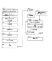
- FIG. 1 shows a flowchart of a method for manufacturing the optical display device according to the first embodiment.
- a configuration that does not include the first and second defect inspection apparatuses can be exemplified.
- liquid crystal cell used in the present invention
- examples of the liquid crystal cell used in the present invention include a glass substrate unit, an organic EL light emitting unit and the like.
- the liquid crystal cell is formed in a rectangular shape, for example.
- the optical film to be bonded to the liquid crystal cell may be a laminated film in which other films such as a retardation film and a brightness enhancement film are combined as long as it includes a polarizer (polarizer film).
- a protective transparent film may be laminated on the surface of the optical film.
- an adhesive layer is formed on one surface of the optical film so as to be attached to the liquid crystal cell, and a release film for protecting the adhesive layer is provided.
- a surface protective film is provided on the other surface of the optical film via an adhesive layer. Specific configurations of these films will be described later.
- an optical film in which a surface protective film and a release film are laminated via an adhesive layer may be referred to as a sheet product.
- the laminated structure of the first sheet product F1 includes a first optical film F11, a first release film F12, and a surface protective film F13.
- the first optical film F11 includes a first polarizer F11a, a first film F11b having an adhesive layer (not shown) on one side thereof, and a second film having an adhesive layer (not shown) on the other side. F11c.
- the first and second films F11b and F11c are, for example, polarizer protective films (for example, triacetyl cellulose film, PET film, etc.).
- the second film F11c is bonded to the liquid crystal cell surface side via the first pressure-sensitive adhesive layer F14.
- a surface treatment can be applied to the first film F11b. Examples of the surface treatment include a hard coat treatment, an antireflection treatment, a treatment for the purpose of prevention of sticking, diffusion or antiglare, and the like.
- the first release film F12 is provided via the second film F11c and the first pressure-sensitive adhesive layer F14.
- the surface protection film F13 is provided through the 1st film F11b and the adhesive layer F15. Specific configurations of the first and second films F11b and F11c will be described later. Below, the laminated structure of a polarizer and a polarizer protective film may be called a polarizing plate.
- the width of the first roll original fabric or the width of the second roll original fabric described later “depends on the bonding size of the liquid crystal cell” means the size of either the long side or the short side of the liquid crystal cell Means to match. “Adjust to the size of either the long side or the short side of the liquid crystal cell” means that the length of the optical film bonded to the length of the long side or the short side of the liquid crystal cell (the length excluding the exposed part) The length of the long side or the short side of the liquid crystal cell and the width of the first roll original fabric or the second roll original fabric need not be the same.
- the following processes are performed in an isolated structure that is isolated in the factory, and the cleanliness is maintained.
- the cleanliness is maintained in the bonding step of bonding the optical film to the liquid crystal cell.
- the defect inspection method includes a method of photographing and processing images with transmitted light and reflected light on both sides of the first sheet product F1, and an inspection polarizing film between the CCD camera and the inspection object.
- An image is taken between the object and an object so as to be at a predetermined angle (for example, a range greater than 0 degree and within 10 degrees) with the polarization axis of the polarizing plate to be inspected.
- -Image processing methods are listed. Note that a known method can be applied to the image processing algorithm, and for example, a defect can be detected by density determination by binarization processing.
- the defect information obtained by the first defect inspection apparatus is linked with the position information (for example, position coordinates), transmitted to the control apparatus, and can contribute to the cutting method by the first cutting apparatus described later. .
- First cutting step (FIG. 1, S4: first cutting step).
- the first cutting device cuts the surface protective film F13, the pressure-sensitive adhesive layer F15, the first optical film F11, and the first pressure-sensitive adhesive layer F14 into a predetermined size without cutting the first release film F12.
- the cutting means include a laser device, a cutter, and other known cutting means. Based on the defect information obtained by the first defect inspection apparatus, it is configured to cut away from the defect so that the defect is not included in the region bonded to the liquid crystal cell W. Thereby, the yield of the first sheet product F1 is greatly improved.
- a method of cutting while avoiding the defect so as not to include the defect in the region bonded to the liquid crystal cell W is called a skip cut.
- defect information at the time of cutting is obtained by an inline defect inspection apparatus. Or may have been previously applied to the roll.
- the first sheet product F ⁇ b> 1 including the defect is excluded by a first rejection device described later, and is not attached to the liquid crystal cell W.
- steps of the first roll original fabric preparation step, the first inspection step, and the first cutting step are preferably continuous production lines.
- the cut first optical film F11 for bonding to one surface of the liquid crystal cell W is formed.
- disconnected 2nd optical film F21 for bonding to the other surface of the liquid crystal cell W is demonstrated.
- disconnected 1st optical film F11 and 2nd optical film F21, respectively is performed in parallel.
- a long second sheet product F2 is prepared as a second roll material.
- the second sheet product F2 includes a second optical film F21, a second release film F22, and a surface protection film F23.
- the second optical film F21 includes a second polarizer 21a, a third film F21b having an adhesive layer (not shown) on one side thereof, and a fourth film having an adhesive layer (not shown) on the other side. F21c.
- the third and fourth films F21b and F21c are, for example, polarizer protective films (for example, triacetyl cellulose film, PET film, etc.).
- the fourth film F21c is bonded to the liquid crystal cell surface side via the second pressure-sensitive adhesive layer F24.
- the third film F21b can be subjected to a surface treatment. Examples of the surface treatment include a hard coat treatment, an antireflection treatment, a treatment for the purpose of prevention of sticking, diffusion or antiglare, and the like.
- the second release film F22 is provided via the fourth film F21c and the second pressure-sensitive adhesive layer F24.
- the surface protection film F23 is provided through the 3rd film F21b and the adhesive layer F25.
- Second inspection step (FIG. 1, S13).
- a defect of the second sheet product F2 is inspected using a second defect inspection apparatus.
- the defect inspection method here is the same as the method using the first defect inspection apparatus described above.
- Second cutting step (FIG. 1, S14: second cutting step).
- the second cutting device cuts the surface protective film F23, the pressure-sensitive adhesive layer F25, the second optical film F21, and the second pressure-sensitive adhesive layer F24 into a predetermined size without cutting the second release film F22.
- the cutting means include a laser device, a cutter, and other known cutting means. Based on the defect information obtained by the second defect inspection apparatus, it is configured so as to avoid the defect and cut the defect so that the defect is not included in the region bonded to the liquid crystal cell W. Thereby, the yield of the second sheet product F2 is greatly improved.
- the second sheet product F ⁇ b> 2 including the defect is excluded by a second rejection device described later, and is not attached to the liquid crystal cell W.
- the process of conveying the liquid crystal cell W is performed in parallel with the process of forming the cut first optical film F11 and the second optical film F21 as described above.
- the liquid crystal cell W is subjected to the following processing during its conveyance.
- Liquid crystal cell alignment step (FIG. 1, S5).
- the liquid crystal cell W is aligned by a panel alignment device so as to be conveyed at a predetermined position.
- disconnected 1st optical film F11 and 2nd optical film F21 are bonded in the following aspects on both surfaces of the liquid crystal cell W conveyed as mentioned above, respectively. ing.
- Optical film alignment step (FIG. 1, S15: film alignment step).
- the first optical film F11 is aligned by a first film alignment device
- the second optical film F21 is aligned by a second film alignment device so as to be conveyed at predetermined positions.
- the optical film alignment process is not limited to the configuration performed after the first cutting process and the second cutting process, but is performed before or in parallel with the first cutting process and the second cutting process. Such a configuration may be adopted.
- Optical film bonding step (FIG. 1, S16: first bonding step, second bonding step).
- first bonding step the cut first optical film F11 is applied to one surface of the liquid crystal cell W via the first adhesive layer F14 by the first bonding device. Bonding is performed (first bonding step).
- second bonding step the bonding step including the first bonding step and the second bonding step is performed by the bonding device including the first bonding device and the second bonding device.
- Optical display device inspection process (FIG. 1, S17).
- the inspection device inspects an optical display device in which an optical film is attached to both surfaces of the liquid crystal cell W.
- Examples of the inspection method include a method of taking an image and processing an image using reflected light on both sides of the optical display device.
- a method of installing a polarizing film for inspection between the CCD camera and the inspection object is also exemplified. Note that a known method can be applied to the image processing algorithm, and for example, a defect can be detected by density determination by binarization processing.
- a non-defective product of the optical display device is determined based on the defect information obtained by the inspection device.
- the optical display device determined to be non-defective is conveyed to the next mounting process. If a defective product is determined, a rework process is performed, a new optical film is applied, and then inspected.If a good product is determined, the process proceeds to a mounting process. Discarded.
- the optical display device can be suitably manufactured by making the bonding step of the first optical film F11 and the bonding step of the second optical film F21 into a continuous production line.
- defect information (defect coordinates, defect type, size, etc.) of the first and second sheet products is coded in a predetermined pitch unit (for example, 1000 mm). It may be attached as information (for example, QR code, barcode). In such a case, before the cutting, the code information is read and analyzed, and cut into a predetermined size in the first and second cutting steps so as to avoid the defective portion.
- the part including the defect is removed or bonded to a member that is not a liquid crystal cell, and a non-defective sheet product cut to a predetermined size is bonded to the liquid crystal cell.
- the yield of optical film F11, F21 is improved significantly.
- Various devices that realize the manufacturing method of Embodiment 1 are isolated from the outside by an isolation structure.
- the inside surrounded by the isolation structure is kept clean compared to the outside.
- the isolation structure is composed of a transparent material wall and a framework structure.
- a blower is installed on the ceiling of the isolation structure.
- the blower device includes a HEPA filter and blows air with high cleanness into the partition wall structure.
- An air discharge opening for discharging the internal air to the outside is provided at the bottom of the wall surface of the partition wall structure.
- a filter can be provided on the opening surface to prevent intruders from the outside.
- the liquid crystal cell W is taken out from the storage box and placed on the transport mechanism.
- the conveyance is stopped and the end of the liquid crystal cell W is held by the holding means.
- the polishing means is brought into contact with the upper surface of the liquid crystal cell W from above and the other polishing means is brought into contact with the lower surface of the liquid crystal cell from below.
- the respective polishing means are rotated on both surfaces of the liquid crystal cell W. As a result, the adhered foreign matter on both surfaces of the liquid crystal cell W is removed. Examples of the adhering foreign matter include glass fine pieces, fiber pieces, and the like.
- the liquid crystal cell W that has been polished and cleaned is transferred to a water bath by a transfer mechanism, where it is cleaned with water. Pure water flows inside the bath. Both surfaces of the liquid crystal cell W conveyed from the water bath are washed with pure water flowing out from the flowing water pipe. Next, the liquid crystal cell W is drained by blowing clean air from a drying device. As another embodiment, it is possible to wash with an aqueous ethanol solution instead of pure water. In another embodiment, the water bath can be omitted.
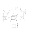
- FIG. 3 is a schematic diagram showing a configuration example for bonding the optical films F11 and F21 to the liquid crystal cell W.
- various devices will be described in order with reference to FIG.
- the liquid crystal cell W cleaned as described above is aligned by the panel alignment apparatus 10 in the process of being transported, and then the optical films F11 and F21 are bonded to both surfaces thereof.
- the panel alignment apparatus 10 includes, for example, one or a plurality of rollers for transporting the liquid crystal cell W and an edge detection unit for detecting the edge of the liquid crystal cell W.
- the panel alignment apparatus 10 causes the liquid crystal cell W to meander by tilting the roller based on the detection result of the edge of the liquid crystal cell W by the edge detection unit, and sets the liquid crystal cell W to a predetermined position. Align so that it is transported.
- the first roll material R1 of the long first sheet product F1 is installed on a roller mount device that is linked to a motor or the like so as to rotate freely or at a constant rotational speed.
- the rotational speed is set by the control device, and the drive is controlled.
- the first transport device 12 is a transport mechanism that transports the first sheet product F1 to the downstream side.
- the first conveying device 12 includes a number of conveying rollers, and the first sheet product F1 is conveyed along a conveying path formed by these conveying rollers. The said conveyance path is extended from the 1st roll original fabric R1 to the 1st bonding apparatus 18.
- FIG. The first transport device 12 is controlled by a control device.
- the first defect inspection apparatus 14 performs defect inspection after the first release film F12 is peeled off.
- the first defect inspection device 14 detects the defect by analyzing the image data picked up by the CCD camera, and further calculates its position coordinates. The position coordinates of this defect are provided for the skip cut by the first cutting device 16 described later.
- the 1st cutting device 16 cut
- the protective film F13, the first pressure-sensitive adhesive layer F14, and the pressure-sensitive adhesive layer F15 are cut into a predetermined size.
- the first cutting device 16 is, for example, a laser device. Based on the position coordinates of the defect detected in the first defect inspection process, the first cutting device 16 cuts to a predetermined size while avoiding the defect portion so as not to include the defect in the region bonded to the liquid crystal cell W. To do.
- the cut product including the defective portion is rejected as a defective product by the first rejecting device in a subsequent process.
- the first cutting device 16 may continuously cut into a predetermined size while ignoring the existence of the defect. In this case, it can be configured such that the portion is removed without being bonded in the bonding process described later.
- the control in this case also depends on the function of the control device.
- the first film alignment device 19 aligns the first optical film F11.
- the first film alignment device 19 includes, for example, one or a plurality of rollers for conveying the first optical film F11, and an edge detection unit for detecting the edge of the cut first optical film F11. ing.
- the first film alignment device 19 causes the first optical film F11 to meander by tilting the roller based on the detection result of the edge of the first optical film F11 by the edge detection unit, and the first optical film. F11 is aligned so that a predetermined position is conveyed.
- the edge detector preferably detects the edge of the tip of the first optical film F11, and the roller is the tip of the first optical film F11. It is preferable to meander the first optical film F11 to some extent on the front side. Therefore, it is preferable that the edge detection unit is provided after the first cutting device 16 and the roller is provided before the first cutting device 16.
- the 1st bonding apparatus 18 is cut
- the first optical film F11 is bonded to the liquid crystal cell W surface while being pressed by a pressing roller and a guide roller. The pressing pressure and driving operation of the pressing roller and guide roller are controlled by a control device.
- the first sheet product after peeling the first release film F12 and peeling the first release film F12 by reversing and transferring the first release film F12. It is configured to send F1 (first optical film F11) to the liquid crystal cell W surface.
- F1 first optical film F11
- the tension is less than 150 N / m, the delivery position of the first optical film F11 is not stable, and if it is more than 1000 N / m, the first release film F12 may be stretched and broken, and the time until press contact is 3 seconds. If it is longer, the end portion of the first optical film F11 peeled from the first release film F12 may be bent and folds or bubbles may be generated.
- the peeled first release film F12 is wound up on a roll. Roll winding control is controlled by a control device.
- the laminating mechanism is composed of a pressing roller and a guide roller arranged opposite to it.
- the guide roller is composed of a rubber roller that is rotationally driven by a motor, and is arranged to be movable up and down.
- a pressing roller made of a metal roller that is rotationally driven by a motor is disposed directly above it.
- the pressing roller is raised to a position higher than the upper surface so as to open a roller interval.
- the guide roller and the pressing roller may both be rubber rollers or metal rollers.
- the liquid crystal cell W is cleaned by various cleaning devices and is transported by the transport mechanism.
- the transport control of the transport mechanism is also controlled by the control device.
- the guide roller moves vertically downward.
- the roller around which the removal film is stretched moves to a fixed position of the guide roller.
- the first sheet product F1 including the defect is adhered to the removal film by moving the pressing roller vertically downward to press the first sheet product F1 including the defect against the removal film.
- the removal film can stick the first sheet product F1 including the defects by using the adhesive force of the first adhesive layer F14 of the first sheet product F1, but an adhesive tape is used as the removal film. It is also possible to do.
- the second optical film F21 (second sheet product F2) is bonded in the same manner to the other surface of the liquid crystal cell W in which the first optical film F11 is bonded to one surface as described above. In the following, the description of the same device configuration will be briefly described.
- the second roll raw material R2 of the long second sheet product F2 is installed on a roller mount device that is linked to a motor or the like so as to rotate freely or at a constant rotational speed.
- the rotational speed is set by the control device, and the drive is controlled.
- the second transport device 22 is a transport mechanism that transports the second sheet product F2 to the downstream side.
- the second conveying device 22 includes a large number of conveying rollers, and the second sheet product F2 is conveyed along a conveying path formed by these conveying rollers.
- the said conveyance path is extended from the 2nd roll original fabric R2 to the 2nd bonding apparatus 28.
- FIG. The second transport device 22 is controlled by the control device, and the transport speed is set to be the same as the transport speed of the first transport device 12.
- the second defect inspection device 24 performs defect inspection after the second release film F22 is peeled off.
- the second defect inspection device 24 analyzes the image data picked up by the CCD camera, detects the defect, and calculates its position coordinates. The position coordinates of this defect are provided for the skip cut by the second cutting device 26 described later.
- the 2nd cutting device 26 cut
- the protective film F23, the second pressure-sensitive adhesive layer F24, and the pressure-sensitive adhesive layer F25 are cut into a predetermined size.
- the second cutting device 26 is, for example, a laser device. Based on the position coordinates of the defect detected in the second defect inspection process, the second cutting device 26 cuts to a predetermined size while avoiding the defect portion so as not to include the defect in the region bonded to the liquid crystal cell W. To do. That is, the cut product including the defective portion is rejected by the second rejecting device as a defective product in a subsequent process.
- the 2nd cutting device 26 may ignore the presence of a fault, and may cut continuously to a predetermined size. In this case, it can be configured such that the portion is removed without being bonded in the bonding process described later.
- the control in this case also depends on the function of the control device.
- the second film alignment device 29 performs alignment of the second optical film F21.
- the second film alignment device 29 includes, for example, one or a plurality of rollers for conveying the second optical film F21, and an edge detection unit for detecting the edge of the cut second optical film F21. ing.
- the second film alignment device 29 causes the second optical film F21 to meander by tilting the roller based on the detection result of the edge of the second optical film F21 by the edge detection unit, and the second optical film. F21 is aligned so that a predetermined position is conveyed.
- the edge detector preferably detects the edge of the tip of the second optical film F21, and the roller is the tip of the second optical film F21. It is preferable that the second optical film F21 meanders to some extent on the near side. Therefore, it is preferable that the edge detection unit is provided after the second cutting device 26 and the roller is provided before the second cutting device 26.
- the 2nd bonding apparatus 28 is cut
- the second optical film F21 is bonded to the liquid crystal cell W surface while being pressed by a pressing roller and a guide roller. The pressing pressure and driving operation of the pressing roller and guide roller are controlled by a control device.
- the second release film F22 is reversed and transferred to peel the second release film F22 and the second sheet product after the second release film F22 is peeled off. It is configured to send F2 (second optical film F21) to the liquid crystal cell W surface. At this time, the state in which a tension of 150 N / m or more and 1000 N / m or less is applied to the second release film F22 and / or the liquid crystal cell W surface after the second release film F22 is peeled off the second optical film F21. By performing the time until the pressure contact is made within 3 seconds, the bonding accuracy of the second optical film F21 can be improved.
- the tension is less than 150 N / m, the delivery position of the second optical film F21 is not stable, and if it is more than 1000 N / m, the second release film F22 may be stretched and broken, and the time until press contact is 3 seconds. If it is longer, the end portion of the first optical film F21 peeled from the second release film F22 may be bent and folds or bubbles may be generated.
- the peeled second release film F22 is wound up on a roll. Roll winding control is controlled by a control device.
- the laminating mechanism is composed of a pressing roller and a guide roller arranged opposite to the pressing roller.
- the guide roller is composed of a rubber roller that is rotationally driven by a motor, and is arranged to be movable up and down.
- a pressing roller made of a metal roller that is rotationally driven by a motor is disposed directly below it.
- the pressing roller is moved to a lower position so as to open a roller interval.
- the guide roller and the pressing roller may both be rubber rollers or metal rollers.
- the optical display device formed by bonding the first and second sheet products to the liquid crystal cell W is conveyed to the inspection device.
- the inspection device performs an inspection on both sides of the optical display device that has been conveyed.
- the light source irradiates the upper surface of the optical display device vertically by the half mirror, and the reflected light image is captured as image data by the CCD camera.
- Another light source irradiates the surface of the optical display device at a predetermined angle, and a reflected light image is captured as image data by a CCD camera.
- Inspection of the opposite surface of the optical display device is similarly performed using a light source and a CCD camera. The defect is subjected to image processing analysis from these image data, and a non-defective product is determined.
- the operation timing of each apparatus is calculated by, for example, a method of detecting by arranging a sensor at a predetermined position, or by detecting a rotary member of the transfer apparatus or the transfer mechanism with a rotary encoder or the like.
- the control device may be realized by a cooperative action of a software program and a hardware resource such as a CPU and a memory.
- a memory is stored in advance for program software, a processing procedure, various settings, and the like. Further, it can be configured by a dedicated circuit or firmware.
- the first film alignment device 19 and the second film alignment device 29 constitute a film alignment device that performs relative alignment between the first optical film F11 and the second optical film F21.
- the first optical film F11 and the second optical film F21 that have been cut are aligned so that the tips of the first optical film F11 and the second optical film F21 are simultaneously guided to the same position in plan view, whereby the first optical film is aligned with the liquid crystal cell W.
- the film F11 and the second optical film F21 are bonded together at the same time.
- the period during which the first bonding device 18 bonds the first optical film F11 to one surface of the liquid crystal cell W, and the second bonding device 28 bonds the second optical film F21 to the other surface of the liquid crystal cell W As long as at least a part of the period to be combined overlaps, it is not necessary to have a configuration in which they are bonded together as described above. According to the configuration in which the above periods partially overlap, the first optical film F11 and the second optical film F21 can be bonded to both surfaces of the liquid crystal cell W in parallel for at least a predetermined period. Accordingly, the first optical film F11 and the second optical film F21 can be bonded simultaneously or continuously in a state where the alignment of the liquid crystal cell W is performed.
- the first optical film F11 and the second optical film Unlike the case where the films F21 are bonded separately, it is not necessary to align the liquid crystal cell W in each bonding. Therefore, the number of alignment devices can be reduced, and the optical films F11 and F21 can be satisfactorily bonded to both surfaces of the liquid crystal cell W with a simpler configuration. It should be noted that the present invention is not limited to a configuration in which the respective periods partially overlap, and a configuration in which the respective periods do not overlap may be employed.
- the automatic inspection apparatus is an apparatus that automatically inspects defects (also referred to as defects) of a sheet product.
- the automatic inspection apparatus emits light, and the reflected light image and the transmitted light image are image sensors such as a line sensor or a two-dimensional TV camera The defect detection is performed based on the acquired image data. Further, the image data is acquired in a state where the inspection polarizing filter is interposed in the optical path between the light source and the imaging unit.
- the polarization axis (for example, the polarization absorption axis) of the polarizing filter for inspection is arranged to be in a state (crossed Nicols) orthogonal to the polarization axis (for example, the polarization absorption axis) of the polarizing plate to be inspected.
- crossed Nicols a black image is input from the imaging unit if there is no defect, but if there is a defect, that part will not be black (recognized as a bright spot). Therefore, a defect can be detected by setting an appropriate threshold value. In such bright spot detection, defects such as surface deposits and internal foreign matter are detected as bright spots.
- the method (half-cut method) for cutting other members of the sheet product without cutting the release film has been described.
- the optical film and the pressure-sensitive adhesive layer are cut without cutting the release film bonded to the optical film via the pressure-sensitive adhesive layer, and before the bonding process to the liquid crystal cell.
- the release film can be peeled from the optical film. That is, since the pressure-sensitive adhesive layer that is the bonding surface of the optical film can be configured not to be exposed until just before the bonding, it is possible to prevent foreign matters from being mixed into the bonding surface of the optical film.
- the cut optical film and the pressure-sensitive adhesive layer can be conveyed using the release film as a carrier. Therefore, since the optical film transport device can be made simpler, the manufacturing cost of the optical display device can be further reduced.
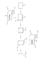
- FIG. 4 is a schematic diagram for explaining the bonding mode of the optical films F11 and F21 to the liquid crystal cell W.
- the 1st optical film F11 and the 2nd optical film F21 consist of a stretched film stretched
- the first roll original fabric R1 is formed by winding the first optical film F11 (first sheet product F1) so that the polarization axis B1 extends in a direction orthogonal to the width direction along the core A1. Yes.
- the width of the first optical film F11 along the core A1 of the first roll original fabric R1 is a length corresponding to the long side of the liquid crystal cell W.
- the 1st conveyance apparatus 12 sends out the 1st optical film F11 from this 1st roll original fabric R1 in the orthogonal direction with respect to the width direction. Then, the fed first optical film F11 is cut in the width direction at intervals corresponding to the short sides of the liquid crystal cell W, so that the first optical film F11 cut into a rectangular shape corresponding to the liquid crystal cell W is obtained. Is formed.
- the second roll original R2 has the second optical axis so that the polarization axis B2 extends in a direction parallel to the width direction along the core A2, that is, in a direction orthogonal to the polarization axis B1 of the first optical film F11. It is formed by winding a film F21 (second sheet product F2).
- the width of the second optical film F21 along the core A2 of the second roll original fabric R2 is the same as the width of the first optical film F11 and corresponds to the long side of the liquid crystal cell W.
- the 1st roll original fabric R1 and the 2nd roll original fabric R2 are arrange
- the 2nd conveyance apparatus 22 sends out the 2nd optical film F21 from this 2nd roll original fabric R2 to the orthogonal direction with respect to the width direction. And the sent 2nd optical film F21 is cut
- the first optical film F11 and the second optical film F21 cut as described above have long and short sides corresponding to the long and short sides of the liquid crystal cell W, respectively. Can be attached to both sides. Thereby, the 1st optical film F11 and the 2nd optical film F21 are bonded together on both surfaces of the liquid crystal cell W so that each polarization axis B1 and B2 may mutually orthogonally cross. Therefore, without providing a mechanism for rotating the liquid crystal cell W, the first optical film F11 and the second optical film F21 bonded to both surfaces of the liquid crystal cell W can be in a crossed Nicols relationship, The optical films F11 and F21 can be satisfactorily bonded to both surfaces of the liquid crystal cell W with a simpler configuration.
- the first optical film F11 is wound so that the polarization axis B1 extends in a direction orthogonal to the width direction
- the second optical film F21 is wound so that the polarization axis B2 extends in the width direction. It is easy to align the polarization axes B1 and B2 of the optical films F11 and F21 with the long side or the short side of the liquid crystal cell W. For this reason, when the optical films F11 and F21 are bonded to the liquid crystal cell W, the possibility that the polarization axes B1 and B2 are shifted becomes low, and the contrast abnormality of the optical display device due to the deviation of the polarization axes B1 and B2 occurs. Therefore, the optical films F11 and F21 can be better bonded to both surfaces of the liquid crystal cell W.
- the first optical film F11 and the second optical film F21 are cut at intervals corresponding to the short sides of the liquid crystal cell W, and the cut optical films F11 and F21 are both surfaces of the liquid crystal cell W.
- the first optical film F11 and the second optical film F21 can be brought into a crossed Nicol relationship by being bonded to each other. Thereby, in order to obtain one piece of the cut first optical film F11, the time for feeding the first optical film F11 from the first roll R1 and the first piece of the cut second optical film F21 are obtained.
- the time for feeding the second optical film F21 from the two-roll original fabric R2 can be made shorter than when cutting at intervals corresponding to the long sides of the liquid crystal cell W, the optical films F11 and F21 are formed on both sides of the liquid crystal cell W. Can be efficiently bonded.
- the optical display device manufactured in the manner as in the present embodiment is mounted on an image display device such as a liquid crystal display device and is visually recognized from one of the front and back surfaces.
- the 1st optical film F11 is bonded to the surface which becomes the front side (viewing side) when visually recognizing the optical display device, and the 2nd optical film F21 becomes the back side (backlight side) when visually recognizing the optical display device. It is preferable to be bonded to the surface.
- the reference example is demonstrated.
- a polarizing plate A having a polarizing axis perpendicular to the width direction is prepared by bonding “TD80UL manufactured by Fuji Film Co., Ltd.” as a polarizer protective film on both sides of the obtained polarizer through a PVA adhesive. did.
- the optical properties of the obtained polarizing plate A were measured with “Spectrophotometer V7100 manufactured by JASCO Corporation”, the transmittance was 41.0% and the polarization degree was 99.997%.
- Preparation of polarizing plate B A polyvinyl alcohol film having a degree of polymerization of 2400 and a thickness of 75 ⁇ m is fed out from the raw material, both ends in the width direction of the PVA film are held by holding means, and the PVA film is transferred at a speed of 1 m / min with a tenter stretching machine. Was conveyed in the longitudinal direction. Using a spraying device that reciprocates in the width direction of the PVA film at 30 m / min, water (swelling liquid) at 30 ° C. was applied for 30 seconds in the gas phase on both sides of the PVA film at a flow rate of 16 mL / min. Sprayed.
- the said PVA film was extended
- a 30 ° C. aqueous solution (dye solution) containing 0.2 wt% iodine was sprayed on one side of the swollen PVA film in the gas phase for 25 seconds.
- the PVA film was stretched in the width direction by the gripping means so as to be 3.3 times as long as the original fabric.
- aqueous solution (conditioning solution) containing 4% by weight of potassium iodide was sprayed on one side of the stretched PVA film for 10 seconds.
- the moisture content of the PVA film is decreased by releasing the PVA film from the gripping means and simultaneously performing a heat drying treatment in a 45 ° C. atmosphere for 1 minute while conveying the PVA film by a roll in the longitudinal direction.
- the length in the longitudinal direction of the PVA film was shrunk to 85% as compared to immediately after opening (shrinkage rate 15%). A total of four rolls were used, and the rotational speed of the rolls was sequentially decreased as going to the downstream side in the traveling direction of the PVA film.
- the rotation speed of each roll was 1.00 m / min, 0.9 m / min, 0.875 m / min, and 0.85 m / min, respectively, from the upstream side in the traveling direction of the PVA film.
- the PVA film after shrinkage was dried at 60 ° C. for 1 minute to obtain a polarizer.
- TD80UL manufactured by Fuji Film Co., Ltd. is unwound from the original fabric and 2,2′-bis (3,4-dicarboxyphenyl) hexafluoropropane ⁇ 6FDA and 2,2′-bis (trifluoromethyl)-
- the slow axis of this base material film A with phase difference was a conveyance direction.
- “TD80UL manufactured by Fuji Film Co., Ltd.” was bonded as a polarizer protective film via a PVA adhesive, and the other side was prepared as a polarizer protective film with a retardation layer on the other side.
- the substrate film A with a phase difference was bonded through a PVA adhesive to prepare a polarizing plate B having a polarization axis parallel to the width direction.
- the optical properties of the obtained polarizing plate B were measured by “Spectrophotometer V7100 manufactured by JASCO Corporation”. As a result, the transmittance was 42.6% and the polarization degree was 99.981%.
- the liquid crystal cell was taken out from “32-inch liquid crystal television BRAVIA (registered trademark) KDL-32F1 manufactured by Sony Corporation”, and the polarizing plates A and B were mounted.
- the polarizing plate A was bonded so that the polarizing axis of the polarizer was in the horizontal direction on the viewing side of the cell.
- a polarizing plate B was bonded to the backlight side of the cell so that the polarization axis was in the vertical direction. At this time, the polarizing plate B was bonded so that the surface of the base film A with retardation was on the cell side.
- the contrast of the obtained television was measured with a “Topcon luminance meter BM-5A”. The contrast was “2546”.
- a polarizer protective film with a retardation layer is attached to one side of the polarizer prepared in the same manner as the polarizing plate A, using a PVA adhesive as a polarizer protective film and “TD80UL manufactured by Fuji Film Co., Ltd.”.
- the substrate film B with retardation prepared above was bonded via a PVA adhesive to prepare a polarizing plate C having a polarization axis perpendicular to the width direction.
- the optical properties of the obtained polarizing plate C were measured by “Spectrophotometer V7100 manufactured by JASCO Corporation”. As a result, the transmittance was 41.0% and the polarization degree was 99.995%.
- polarizing plate D “FD80UL manufactured by Fuji Film Co., Ltd.” as a polarizer protective film is bonded to both sides of a polarizer prepared in the same manner as polarizing plate B with a PVA adhesive, and the width direction is A polarizing plate D having a parallel polarization axis was prepared.
- the optical properties of the obtained polarizing plate D were measured by “Spectrophotometer V7100 manufactured by JASCO Corporation”, the transmittance was 42.6% and the degree of polarization was 99.983%.
- the liquid crystal cell was taken out from “32-inch liquid crystal television BRAVIA (registered trademark) KDL-32F1 manufactured by Sony Corporation” and the polarizing plates C and D were mounted.
- the polarizing plate D was bonded so that the polarizing axis of the polarizer was in the horizontal direction on the viewing side of the cell.
- the polarizing plate C was bonded to the backlight side of the cell so that the polarization axis was in the vertical direction.
- the polarizing plate C was bonded so that the surface of the base film B with retardation was on the cell side.
- the contrast of the obtained television was measured with a “Topcon luminance meter BM-5A”.
- the contrast was “2173”. It can be seen that the contrast “2173” in the reference example 2 is inferior to the contrast “2546” in the reference example 1.
- a polarizing plate will be described as an example of an optical film.
- a TAC (triacetyl cellulose) film (polarizer protective film) is bonded to one side of a polyvinyl alcohol film (polarizer) manufactured in advance, and a PET (polyethylene terephthalate) film is bonded to the other side. It is obtained by combining.
- the roll of the polarizing plate is manufactured, for example, by the following manufacturing process.
- A a step of obtaining a polarizer.
- a polarizer is obtained by drying a polyvinyl alcohol (PVA) film subjected to dyeing / crosslinking and stretching treatment.
- B The process of manufacturing a polarizing plate.
- a TAC film is bonded to one side of a polarizer via an adhesive, and a PET film is bonded to the other side and dried to produce a polarizing plate.
- Anti-glare treatment may be applied in advance to the PET film on the viewing side of the display device.
- C The process of bonding a release film (separator) and a protective film together.
- a separator is bonded to the TAC film surface of the polarizing plate via a strong pressure-sensitive adhesive layer, and a surface protective film is bonded to the PET film surface via a weak pressure-sensitive adhesive layer.
- a strong pressure-sensitive adhesive layer is applied in advance to the separator, and a weak pressure-sensitive adhesive layer is applied to the surface protective film.
- the strong pressure-sensitive adhesive layer applied to the separator is transferred to the TAC film after peeling the separator.
- the weak pressure-sensitive adhesive layer applied to the surface protective film remains formed on the surface protective film even when the surface protective film is peeled off, and is not substantially transferred to the PET film.
- a long sheet product is manufactured, wound into a roll, and provided to the post-process.
- a predetermined inspection is performed by an inspector for each process.
- the inspector visually confirms defects (foreign matter, dirt, twist, etc.) during the conveyance of the PVA original fabric.
- the inspector visually observes a defect (foreign matter, dirt, nick, twist, Check for kinks.
- a defect inspection device (a well-known device that photographs foreign matter, dirt, etc. with a camera, and processes the image to determine the defect) automatically inspects the original polarizing plate after bonding and confirms the defect on the monitor. .
- step (C) when winding the obtained strip-shaped sheet product in a roll, the inspector visually confirms defects (foreign matter, dirt, twist, etc.) at the start and end of winding of the roll.
- the sheet product is rated (good, defective, whether shipment is possible) by evaluating this defect.
- (D) a slit process of the roll material Since the roll stock is wide, the roll stock is slit to a predetermined size in accordance with the size of the optical display device as the final product. Depending on the width of the roll, the slit process is omitted.
- a roll type automatic inspection device and / or a visual inspection by an inspector is performed as a visual inspection of a long sheet product.
- the roll type automatic inspection device is a known device that takes a winding defect, an appearance defect, and the like with a camera, and performs image processing to determine a defect.
- the manufactured roll material is packed and transported to the next process place.
- the bonding process with the liquid crystal cell is performed at the same place, it is transported to the next process in simple packaging or as it is.
- the optical display device manufactured according to the present invention can be applied to image display devices such as liquid crystal display devices, organic EL display devices, and PDPs.
- a liquid crystal display device is generally formed by assembling components such as a liquid crystal cell, an optical film, and an illumination system as necessary, and incorporating a drive circuit.
- the present invention is effective when the liquid crystal cell is a VA mode or IPS mode liquid crystal cell, for example.
- Appropriate liquid crystal display devices such as a liquid crystal display device in which an optical film is disposed on one side or both sides of a liquid crystal cell, and a backlight or reflector used in an illumination system can be formed.
- the optical film can be installed on one side or both sides of the liquid crystal cell.
- they may be the same or different.
- a liquid crystal display device for example, a single layer or a suitable part such as a diffusing plate, an antiglare layer, an antireflection film, a protective plate, a prism array, a lens array sheet, a light diffusing plate, a backlight, etc. Two or more layers can be arranged.
- the liquid crystal display device can be formed as an optical film having an appropriate structure according to the conventional transmission type or reflective type in which an optical film is disposed on one side or both sides of a liquid crystal cell, or a transmissive / reflective type. Therefore, the liquid crystal cell forming the liquid crystal display device is arbitrary, and for example, a liquid crystal cell of an appropriate type such as an active matrix driving type typified by a thin film transistor type may be used.
- liquid crystal display device When providing polarizing plates and optical members on both sides of the liquid crystal cell, they may be the same or different. Furthermore, when forming the liquid crystal display device, for example, appropriate components such as a prism array sheet, a lens array sheet, a light diffusion plate, and a backlight can be arranged in one or more layers at appropriate positions.
Landscapes
- Physics & Mathematics (AREA)
- Nonlinear Science (AREA)
- Chemical & Material Sciences (AREA)
- Crystallography & Structural Chemistry (AREA)
- General Physics & Mathematics (AREA)
- Optics & Photonics (AREA)
- Mathematical Physics (AREA)
- Engineering & Computer Science (AREA)
- Manufacturing & Machinery (AREA)
- Liquid Crystal (AREA)
- Polarising Elements (AREA)
- Devices For Indicating Variable Information By Combining Individual Elements (AREA)
Abstract
Description
16 第1切断装置
18 第1貼合装置
19 第1フィルム位置合わせ装置
22 第2搬送装置
26 第2切断装置
28 第2貼合装置
29 第2フィルム位置合わせ装置
F11 第1光学フィルム
F21 第2光学フィルム
R1 第1ロール原反
A1 巻芯
B1 偏光軸
R2 第2ロール原反
A2 巻芯
B2 偏光軸
W 液晶セル
本発明の実施形態1について以下に説明する。図1に実施形態1の光学表示装置の製造方法のフローチャートを示す。実施形態1の製造システムの別実施形態として、第1・第2欠点検査装置を備えていない構成も例示できる。
まず、本発明に用いられる液晶セルは、例えば、ガラス基板ユニット、有機EL発光体ユニット等を含むものが挙げられる。液晶セルは、例えば長方形状に形成される。
液晶セルに貼り合せられる光学フィルムは、偏光子(偏光子フィルム)を含むものであれば、位相差フィルム、輝度向上フィルムなどの他のフィルムが組み合わせられた積層フィルムであってもよい。光学フィルムの表面には、保護用の透明フィルムが積層される場合がある。また、光学フィルムの一方表面には、液晶セルに貼り付けられるように、粘着剤層が形成され、この粘着剤層を保護するための離型フィルムが設けられる。また、光学フィルムのその他方表面には、粘着剤層を介して表面保護フィルムが設けられる。これらフィルムの具体的構成は後述する。以下において、表面保護フィルムおよび離型フィルムが粘着剤層を介して積層された光学フィルムをシート製品と称することがある。
(1)第1ロール原反準備工程(図1、S1)。長尺の第1シート製品を第1ロール原反として準備する。第1ロール原反の幅は、液晶セルの貼り合わせサイズに依存している。図2に示すように、第1シート製品F1の積層構造は、第1光学フィルムF11と、第1離型フィルムF12と、表面保護フィルムF13とを有する。第1光学フィルムF11は、第1偏光子F11aと、その一方面に接着剤層(不図示)を介した第1フィルムF11bと、その他方面に接着剤層(不図示)を介した第2フィルムF11cとで構成されている。
また、上記第1切断工程および第2切断工程の別実施形態を以下に説明する。第1および第2ロール原反の幅方向の一方の端部には、所定ピッチ単位(例えば1000mm)に第1、第2シート製品の欠点情報(欠点座標、欠点の種類、サイズ等)がコード情報(例えばQRコード、バーコード)として付されている場合がある。このような場合、切断する前段階で、このコード情報を読み取り、解析して欠点部分を避けるように、第1、第2切断工程において所定サイズに切断する。そして、欠点を含む部分は除去あるいは液晶セルではない部材に貼り合わせるように構成し、所定サイズに切断された良品判定の枚葉のシート製品を液晶セルに貼り合わされるように構成する。これにより、光学フィルムF11,F21の歩留まりが大幅に向上される。
以下に、実施形態1の製造方法を実現する好適な製造システムの一例について説明する。
欠点検査は公知の欠点検査方法が適用できる。自動検査装置は、シート製品の欠点(欠陥とも称される)を自動で検査する装置であり、光を照射し、その反射光像や透過光像をラインセンサーや2次元TVカメラなどの撮像部を介して取得し、取得された画像データに基づいて、欠点検出を行う。また、光源と撮像部の間の光路中に検査用偏光フィルタを介在させた状態で画像データを取得する。通常、この検査用偏光フィルタの偏光軸(例えば、偏光吸収軸)は、検査対象である偏光板の偏光軸(例えば、偏光吸収軸)と直交する状態(クロスニコル)となるように配置される。クロスニコルに配置することで、仮に欠点が存在しなければ撮像部から全面黒の画像が入力されるが、欠点が存在すれば、その部分が黒にならない(輝点として認識される)。従って、適宜のしきい値を設定することで、欠点を検出することができる。このような輝点検出では、表面付着物、内部の異物等の欠点が輝点として検出される。また、この輝点検出のほかに、対象物に対して透過光画像をCCD撮像し画像解析することで異物検出する方法もある。また、対象物に対して反射光画像をCCD撮像し画像解析することで表面付着異物を検出する方法もある。
偏光板Aの作成:重合度2700、厚さ75μmのポリビニルアルコールフィルムを原反から繰り出し、30℃の水浴中で1分間膨潤させつつ搬送方向に1.2倍に延伸した後、30℃のヨウ化カリウム濃度0.03%、ヨウ素濃度0.3%の水溶液中で60秒間浸漬して染色しながら、フィルム搬送方向にトータルで3倍に延伸した。次いで、60℃のホウ酸濃度4%、ヨウ化カリウム濃度5%の水溶液中に30秒間浸漬しながらトータルで6倍に延伸した。最後に、30℃のヨウ化カリウム濃度2%の水溶液中に数秒浸漬することで洗浄し、得られた延伸フィルムを70℃で2分間乾燥することで偏光子を得た。得られた偏光子の両面に、偏光子保護フィルムとして「富士フィルム社製TD80UL」をPVA系接着剤を介して貼り合せて、幅方向に対して直交方向の偏光軸を有する偏光板Aを作成した。得られた偏光板Aの光学特性を「日本分光製分光光度計V7100」で測定したところ、透過率41.0%、偏光度99.997%であった。
偏光板Cの作成:基材フィルムとして「富士フィルム社製TD80UL」を原反から繰り出し、2,2’-ビス(3,4-ジカルボキシフェニル)ヘキサフルオロプロパン≒6FDA及び2,2’-ビス(トリフルオロメチル)-4,4’-ジアミノビフェニル≒PFMB≒TFMBから合成された、ポリイミドを溶媒にシクロヘキサノンを用い15wt%で調製した溶液を20μmの厚みで塗布した。その後100℃で10min乾燥処理することで、厚み約3μmの薄膜を有する薄膜付基材フィルムを得た。得られた薄膜付基材フィルムの位相差を「王子計測製KOBRA(登録商標)21ADH」を使用して測定したところ、正面位相差1.2nm、厚み方向位相差188nmであった。この薄膜付基材フィルムを160℃で幅方向に1.19倍に固定端1軸延伸(テンター延伸)して、位相差付基材フィルムBを作成した。得られた位相差付基材フィルムBの位相差を「王子計測製KOBRA(登録商標)21ADH」を使用して測定したところ正面位相差56nm、厚み方向位相差270nmであった。なお、この位相差付基材フィルムBの遅相軸は、幅方向であった。上記偏光板Aと同様に作成した偏光子の片面に、偏光子保護フィルムとして「富士フィルム社製TD80UL」をPVA系接着剤を介して貼り合せ、他方面に、位相差層付偏光子保護フィルムとして前記で作成した位相差付基材フィルムBをPVA系接着剤を介して貼り合せて、幅方向に対して直交方向の偏光軸を有する偏光板Cを作成した。得られた偏光板Cの光学特性を「日本分光製分光光度計V7100」で測定したところ、透過率41.0%、偏光度99.995%であった。
まず、光学フィルムの一例として偏光板について説明する。偏光板は、予め製造しておいたポリビニルアルコール系フィルム(偏光子)の片面に例えばTAC(トリアセチルセルロース)フィルム(偏光子保護フィルム)を貼り合わせ、他方面にPET(ポリエチレンテレフタレート)フィルムを貼り合せることで得られる。
Claims (12)
- 偏光子を含む光学フィルムが巻回されることにより形成されたロール原反から前記光学フィルムを送り出し、幅方向に前記光学フィルムを切断することによって、所定サイズに切断して液晶セルに貼り合せることにより光学表示装置を製造するための光学表示装置製造システムであって、
前記液晶セルの長辺又は短辺に対応する幅の第1光学フィルムを前記幅方向に対して直交方向に偏光軸が延びるように巻回することにより形成された第1ロール原反から、前記直交方向に前記第1光学フィルムを送り出す第1搬送装置と、
前記第1ロール原反に対して幅方向が互いに平行になるように配置され、前記第1光学フィルムと同一の幅を有する第2光学フィルムを前記幅方向に偏光軸が延びるように巻回することにより形成された第2ロール原反から、その幅方向に対して直交方向に前記第2光学フィルムを送り出す第2搬送装置と、
前記第1搬送装置により送り出される第1光学フィルムを前記所定サイズである前記液晶セルの短辺又は長辺に対応する間隔で切断する第1切断装置と、
前記第2搬送装置により送り出される第2光学フィルムを前記第1光学フィルムと同一の間隔で切断する第2切断装置と、
前記切断された前記第1光学フィルムを前記液晶セルの一方の面に貼り合せる第1貼合装置と、
前記切断された前記第2光学フィルムを前記液晶セルの他方の面に貼り合せる第2貼合装置とを備えたことを特徴とする光学表示装置製造システム。 - 前記第1貼合装置が前記液晶セルの前記一方の面に前記第1光学フィルムを貼り合わせる期間と、前記第2貼合装置が当該液晶セルの前記他方の面に前記第2光学フィルムを貼り合わせる期間とが、少なくとも一部重複していることを特徴とする請求項1に記載の光学表示装置製造システム。
- 前記第1光学フィルムの幅と、前記第2光学フィルムの幅とが、それぞれ前記液晶セルの長辺に対応する長さであることを特徴とする請求項1又は2に記載の光学表示装置製造システム。
- 前記第1光学フィルムの幅と、前記第2光学フィルムの幅とが、それぞれ前記液晶セルの短辺に対応する長さであることを特徴とする請求項1又は2に記載の光学表示装置製造システム。
- 前記液晶セルに対して、前記第1光学フィルムが、前記光学表示装置を視認する際に表側となる面に貼り合せられ、前記第2光学フィルムが、前記光学表示装置を視認する際に裏側となる面に貼り合せられることを特徴とする請求項1に記載の光学表示装置製造システム。
- 前記第1光学フィルムと前記第2光学フィルムとの相対的な位置合わせを行うフィルム位置合わせ装置を備えたことを特徴とする請求項1に記載の光学表示装置製造システム。
- 偏光子を含む光学フィルムが巻回されることにより形成されたロール原反から前記光学フィルムを送り出し、幅方向に前記光学フィルムを切断することによって、所定サイズに切断して液晶セルに貼り合せることにより光学表示装置を製造するための光学表示装置製造方法であって、
前記液晶セルの長辺又は短辺に対応する幅の第1光学フィルムを前記幅方向に対して直交方向に偏光軸が延びるように巻回することにより形成された第1ロール原反から、前記直交方向に前記第1光学フィルムを送り出す第1搬送ステップと、
前記第1ロール原反に対して幅方向が互いに平行になるように配置され、前記第1光学フィルムと同一の幅を有する第2光学フィルムを前記幅方向に偏光軸が延びるように巻回することにより形成された第2ロール原反から、その幅方向に対して直交方向に前記第2光学フィルムを送り出す第2搬送ステップと、
前記第1搬送ステップにより送り出される第1光学フィルムを前記所定サイズである前記液晶セルの短辺又は長辺に対応する間隔で切断する第1切断ステップと、
前記第2搬送ステップにより送り出される第2光学フィルムを前記第1光学フィルムと同一の間隔で切断する第2切断ステップと、
前記切断された前記第1光学フィルムを前記液晶セルの一方の面に貼り合せる第1貼合ステップと、
前記切断された前記第2光学フィルムを前記液晶セルの他方の面に貼り合せる第2貼合ステップとを備えたことを特徴とする光学表示装置製造方法。 - 前記第1貼合ステップで前記液晶セルの前記一方の面に前記第1光学フィルムを貼り合わせる期間と、前記第2貼合ステップで当該液晶セルの前記他方の面に前記第2光学フィルムを貼り合わせる期間とが、少なくとも一部重複していることを特徴とする請求項7に記載の光学表示装置製造方法。
- 前記第1光学フィルムの幅と、前記第2光学フィルムの幅とが、それぞれ前記液晶セルの長辺に対応する長さであることを特徴とする請求項7又は8に記載の光学表示装置製造方法。
- 前記第1光学フィルムの幅と、前記第2光学フィルムの幅とが、それぞれ前記液晶セルの短辺に対応する長さであることを特徴とする請求項7又は8に記載の光学表示装置製造方法。
- 前記液晶セルに対して、前記第1光学フィルムが、前記光学表示装置を視認する際に表側となる面に貼り合せられ、前記第2光学フィルムが、前記光学表示装置を視認する際に裏側となる面に貼り合せられることを特徴とする請求項7に記載の光学表示装置製造方法。
- 前記第1光学フィルムと前記第2光学フィルムとの相対的な位置合わせを行うフィルム位置合わせステップを備えたことを特徴とする請求項7に記載の光学表示装置製造方法。
Priority Applications (3)
| Application Number | Priority Date | Filing Date | Title |
|---|---|---|---|
| CN2009801094817A CN101978406B (zh) | 2008-04-14 | 2009-04-13 | 光学显示装置制造系统及光学显示装置制造方法 |
| EP09732742A EP2270770A1 (en) | 2008-04-14 | 2009-04-13 | Optical display device manufacturing system and method for manufacturing optical display device |
| US12/900,940 US8427625B2 (en) | 2008-04-14 | 2010-10-08 | Optical display device manufacturing system and method for manufacturing optical display device |
Applications Claiming Priority (4)
| Application Number | Priority Date | Filing Date | Title |
|---|---|---|---|
| JP2008-104961 | 2008-04-14 | ||
| JP2008104961 | 2008-04-14 | ||
| JP2009095562A JP4855493B2 (ja) | 2008-04-14 | 2009-04-10 | 光学表示装置製造システム及び光学表示装置製造方法 |
| JP2009-095562 | 2009-04-10 |
Related Child Applications (1)
| Application Number | Title | Priority Date | Filing Date |
|---|---|---|---|
| US12/900,940 Continuation-In-Part US8427625B2 (en) | 2008-04-14 | 2010-10-08 | Optical display device manufacturing system and method for manufacturing optical display device |
Publications (1)
| Publication Number | Publication Date |
|---|---|
| WO2009128416A1 true WO2009128416A1 (ja) | 2009-10-22 |
Family
ID=41199108
Family Applications (1)
| Application Number | Title | Priority Date | Filing Date |
|---|---|---|---|
| PCT/JP2009/057430 WO2009128416A1 (ja) | 2008-04-14 | 2009-04-13 | 光学表示装置製造システム及び光学表示装置製造方法 |
Country Status (7)
| Country | Link |
|---|---|
| US (1) | US8427625B2 (ja) |
| EP (1) | EP2270770A1 (ja) |
| JP (1) | JP4855493B2 (ja) |
| KR (1) | KR101586101B1 (ja) |
| CN (1) | CN101978406B (ja) |
| TW (1) | TWI459096B (ja) |
| WO (1) | WO2009128416A1 (ja) |
Cited By (3)
| Publication number | Priority date | Publication date | Assignee | Title |
|---|---|---|---|---|
| US20140085723A1 (en) * | 2011-05-20 | 2014-03-27 | Nitto Denko Corporation | Optical film roll set, and method for producing optical film roll set |
| CN104169756A (zh) * | 2012-03-14 | 2014-11-26 | 日东电工株式会社 | 光学膜卷筒 |
| TWI570452B (zh) * | 2011-05-20 | 2017-02-11 | Nitto Denko Corp | A continuous manufacturing method of an optical display panel and a continuous manufacturing system for an optical display panel |
Families Citing this family (32)
| Publication number | Priority date | Publication date | Assignee | Title |
|---|---|---|---|---|
| JP4734515B1 (ja) * | 2009-12-28 | 2011-07-27 | 住友化学株式会社 | 光学表示装置の製造システムおよび当該光学表示装置の製造方法 |
| KR20130036183A (ko) * | 2010-02-24 | 2013-04-11 | 수미토모 케미칼 컴퍼니 리미티드 | 액정 표시 장치의 제조 방법 |
| TWI439756B (zh) * | 2010-11-17 | 2014-06-01 | Chunghwa Picture Tubes Ltd | 面板導電膜配置系統及其方法 |
| JP4921597B1 (ja) * | 2011-03-18 | 2012-04-25 | 日東電工株式会社 | 液晶表示パネルの連続製造システムおよび液晶表示パネルの連続製造方法、並びに、検査装置および検査方法 |
| JP5311425B2 (ja) * | 2011-11-11 | 2013-10-09 | 住友化学株式会社 | 光学フィルムチップの切り出し装置及び光学フィルムチップの切り出し方法 |
| KR101477453B1 (ko) * | 2011-11-21 | 2014-12-29 | 수미토모 케미칼 컴퍼니 리미티드 | 광학 부재 접합체의 제조 시스템, 제조 방법 및 기록 매체 |
| CN103890827B (zh) * | 2011-11-21 | 2016-06-08 | 住友化学株式会社 | 光学显示设备的生产系统以及生产方法 |
| WO2013077348A1 (ja) * | 2011-11-21 | 2013-05-30 | 住友化学株式会社 | 光学部材貼合体の製造システム、製造方法及び記録媒体 |
| TWI614200B (zh) * | 2011-11-30 | 2018-02-11 | 住友化學股份有限公司 | 光學顯示設備之生產系統及其生產方法 |
| JP6145893B2 (ja) * | 2012-02-29 | 2017-06-14 | 住友化学株式会社 | 光学表示デバイスの生産システム及び光学表示デバイスの生産方法 |
| KR101608164B1 (ko) * | 2012-02-29 | 2016-04-11 | 수미토모 케미칼 컴퍼니 리미티드 | 광학 표시 디바이스의 생산 시스템 및 광학 표시 디바이스의 생산 방법 |
| JP6245817B2 (ja) | 2012-03-14 | 2017-12-13 | 日東電工株式会社 | 光学フィルムロール |
| JP6112921B2 (ja) * | 2012-03-14 | 2017-04-12 | 日東電工株式会社 | 液晶表示パネルの製造方法 |
| JP6172980B2 (ja) * | 2012-03-14 | 2017-08-02 | 日東電工株式会社 | 液晶表示パネルの製造方法 |
| JP5307947B1 (ja) * | 2012-03-30 | 2013-10-02 | 日東電工株式会社 | 液晶表示装置の製造方法 |
| TWI582491B (zh) * | 2012-08-08 | 2017-05-11 | 住友化學股份有限公司 | 光學顯示設備之生產系統及生產方法 |
| JP5733547B2 (ja) * | 2012-09-07 | 2015-06-10 | 住友化学株式会社 | 光学部材貼合体の製造装置 |
| KR101932562B1 (ko) * | 2012-09-18 | 2018-12-28 | 삼성디스플레이 주식회사 | 필름 부착장치 및 그것을 이용한 필름 부착방법 |
| JP5724146B2 (ja) * | 2013-05-16 | 2015-05-27 | 住友化学株式会社 | 光学部材貼合体の製造システム、製造方法及び記録媒体 |
| JP6178660B2 (ja) * | 2013-08-08 | 2017-08-09 | 住友化学株式会社 | 光学表示デバイスの生産システム |
| US9694571B2 (en) | 2014-01-08 | 2017-07-04 | Lg Chem, Ltd. | System for laminating optical film and method for manufacturing display unit using the same |
| WO2015105242A1 (ko) * | 2014-01-08 | 2015-07-16 | 주식회사 엘지화학 | 광학 필름 라미네이팅 시스템 및 이를 이용한 디스플레이 유닛 제조방법 |
| KR101540431B1 (ko) * | 2014-01-08 | 2015-07-30 | 주식회사 엘지화학 | 광학 필름 라미네이팅 시스템 및 이를 이용한 디스플레이 유닛 제조방법 |
| US9682543B2 (en) | 2014-01-08 | 2017-06-20 | Lg Chem, Ltd. | System for laminating optical film and method for manufacturing display unit using the same |
| KR101495763B1 (ko) * | 2014-02-28 | 2015-02-25 | 주식회사 엘지화학 | 광학 필름 라미네이팅 시스템 및 이를 이용한 디스플레이 유닛 제조방법 |
| US10385686B2 (en) * | 2014-10-28 | 2019-08-20 | Eog Resources, Inc. | Completions index analysis |
| JP2016157081A (ja) * | 2015-02-26 | 2016-09-01 | 日東電工株式会社 | 位相差層付偏光板および画像表示装置 |
| JP6795318B2 (ja) | 2016-03-28 | 2020-12-02 | 日東電工株式会社 | 片保護偏光フィルム、粘着剤層付偏光フィルム、画像表示装置およびその連続製造方法 |
| CN106098698B (zh) * | 2016-06-21 | 2019-06-04 | 京东方科技集团股份有限公司 | 阵列基板及其制作方法、显示装置 |
| JP6654113B2 (ja) * | 2016-07-22 | 2020-02-26 | 日東電工株式会社 | 光学表示パネルの製造方法と光学表示パネルの製造システム |
| CN108776407B (zh) * | 2018-05-31 | 2021-08-27 | 信利光电股份有限公司 | 一种显示模组及终端 |
| JP7141340B2 (ja) | 2019-01-04 | 2022-09-22 | 俊樹 松井 | 物体の支持装置 |
Citations (4)
| Publication number | Priority date | Publication date | Assignee | Title |
|---|---|---|---|---|
| JP2004333647A (ja) * | 2003-05-01 | 2004-11-25 | Fuji Photo Film Co Ltd | 光学フィルム貼付装置、方法及び基板 |
| JP2005037416A (ja) | 2003-05-16 | 2005-02-10 | Fuji Photo Film Co Ltd | 偏光板貼合方法及び装置 |
| JP2005037417A (ja) | 2002-06-28 | 2005-02-10 | Fuji Photo Film Co Ltd | 偏光板貼合方法及び装置 |
| JP2007140046A (ja) | 2005-11-17 | 2007-06-07 | Nitto Denko Corp | 光学表示装置の製造システム及びその製造方法 |
Family Cites Families (14)
| Publication number | Priority date | Publication date | Assignee | Title |
|---|---|---|---|---|
| KR20040002796A (ko) * | 2002-06-28 | 2004-01-07 | 후지 샤신 필름 가부시기가이샤 | 편광판 점착방법 및 그 장치 |
| US20040041968A1 (en) * | 2002-08-30 | 2004-03-04 | Fuji Photo Film Co., Ltd. | Retardation plate and its manufacturing method, circularly polarizing plate and 1/2 wave plate using same, and a reflective liquid crystal display |
| JP4888931B2 (ja) * | 2003-08-08 | 2012-02-29 | 日東電工株式会社 | 液晶表示装置用重畳フィルムの製造方法、液晶表示装置用重畳フィルム及び液晶表示装置 |
| KR101130930B1 (ko) | 2003-11-21 | 2012-03-29 | 니폰 제온 가부시키가이샤 | 액정 표시 장치 |
| JP2005242345A (ja) * | 2004-01-30 | 2005-09-08 | Nippon Zeon Co Ltd | 液晶表示装置 |
| WO2006001448A1 (ja) | 2004-06-29 | 2006-01-05 | Sharp Kabushiki Kaisha | 位相差フィルム、偏光フィルム、液晶表示装置、及び、位相差フィルムの設計方法 |
| JP2006189781A (ja) * | 2004-12-08 | 2006-07-20 | Nitto Denko Corp | 液晶パネル及び液晶表示装置 |
| JP4771692B2 (ja) * | 2004-12-28 | 2011-09-14 | 富士フイルム株式会社 | 液晶表示装置 |
| WO2006070936A1 (en) | 2004-12-28 | 2006-07-06 | Fujifilm Corporation | Liquid crystal display device, optical compensatory sheet, and polarizer and liquid crystal display device employing the same |
| TWI377401B (en) * | 2005-01-25 | 2012-11-21 | Sumitomo Chemical Co | Liquid crystal display device and polarizing plate set useful for the same |
| JP2007225648A (ja) * | 2006-02-21 | 2007-09-06 | Sumitomo Chemical Co Ltd | 広視野角複合偏光板及び液晶表示装置 |
| JP4450011B2 (ja) * | 2006-05-29 | 2010-04-14 | 日東電工株式会社 | 液晶パネル及び液晶表示装置 |
| JP2008003188A (ja) * | 2006-06-21 | 2008-01-10 | Fujifilm Corp | 偏光板の製造方法,及び液晶表示装置 |
| JP4822432B2 (ja) * | 2006-07-25 | 2011-11-24 | 日東電工株式会社 | 液晶パネル、及び液晶表示装置 |
-
2009
- 2009-04-10 JP JP2009095562A patent/JP4855493B2/ja active Active
- 2009-04-13 CN CN2009801094817A patent/CN101978406B/zh active Active
- 2009-04-13 EP EP09732742A patent/EP2270770A1/en not_active Withdrawn
- 2009-04-13 KR KR1020107017497A patent/KR101586101B1/ko active IP Right Grant
- 2009-04-13 WO PCT/JP2009/057430 patent/WO2009128416A1/ja active Application Filing
- 2009-04-14 TW TW098112383A patent/TWI459096B/zh active
-
2010
- 2010-10-08 US US12/900,940 patent/US8427625B2/en not_active Expired - Fee Related
Patent Citations (4)
| Publication number | Priority date | Publication date | Assignee | Title |
|---|---|---|---|---|
| JP2005037417A (ja) | 2002-06-28 | 2005-02-10 | Fuji Photo Film Co Ltd | 偏光板貼合方法及び装置 |
| JP2004333647A (ja) * | 2003-05-01 | 2004-11-25 | Fuji Photo Film Co Ltd | 光学フィルム貼付装置、方法及び基板 |
| JP2005037416A (ja) | 2003-05-16 | 2005-02-10 | Fuji Photo Film Co Ltd | 偏光板貼合方法及び装置 |
| JP2007140046A (ja) | 2005-11-17 | 2007-06-07 | Nitto Denko Corp | 光学表示装置の製造システム及びその製造方法 |
Cited By (7)
| Publication number | Priority date | Publication date | Assignee | Title |
|---|---|---|---|---|
| US20140085723A1 (en) * | 2011-05-20 | 2014-03-27 | Nitto Denko Corporation | Optical film roll set, and method for producing optical film roll set |
| US9261709B2 (en) * | 2011-05-20 | 2016-02-16 | Nitto Denko Corporation | Optical film roll set, and method for producing optical film roll set |
| TWI570452B (zh) * | 2011-05-20 | 2017-02-11 | Nitto Denko Corp | A continuous manufacturing method of an optical display panel and a continuous manufacturing system for an optical display panel |
| US9575343B2 (en) | 2011-05-20 | 2017-02-21 | Nitto Denko Corporation | Method for continuously producing optical display panel, and system for continuously producing optical display panel |
| CN104169756A (zh) * | 2012-03-14 | 2014-11-26 | 日东电工株式会社 | 光学膜卷筒 |
| CN104169756B (zh) * | 2012-03-14 | 2016-11-23 | 日东电工株式会社 | 光学膜卷筒、光学膜卷筒套组以及光学膜卷筒的制造方法 |
| US9581743B2 (en) | 2012-03-14 | 2017-02-28 | Nitto Denko Corporation | Optical film roll |
Also Published As
| Publication number | Publication date |
|---|---|
| KR20110007085A (ko) | 2011-01-21 |
| EP2270770A1 (en) | 2011-01-05 |
| CN101978406A (zh) | 2011-02-16 |
| US8427625B2 (en) | 2013-04-23 |
| KR101586101B1 (ko) | 2016-01-15 |
| TWI459096B (zh) | 2014-11-01 |
| JP2009276757A (ja) | 2009-11-26 |
| TW200951580A (en) | 2009-12-16 |
| CN101978406B (zh) | 2013-10-09 |
| US20110025958A1 (en) | 2011-02-03 |
| JP4855493B2 (ja) | 2012-01-18 |
Similar Documents
| Publication | Publication Date | Title |
|---|---|---|
| JP4855493B2 (ja) | 光学表示装置製造システム及び光学表示装置製造方法 | |
| JP4307510B1 (ja) | 光学表示装置の製造システム及び製造方法 | |
| JP5580750B2 (ja) | 光学表示装置の製造方法、及びそれに用いるロール原反 | |
| JP4628488B1 (ja) | 光学表示装置の製造システム及び製造方法 | |
| JP4629156B2 (ja) | 光学表示装置の製造システム及び製造方法、並びに、ロール原反セット及びその製造方法 | |
| JP4406043B2 (ja) | ロール原反セット、及びロール原反の製造方法 | |
| JP4669070B2 (ja) | 光学表示装置の製造システム及び製造方法 | |
| JP4568375B2 (ja) | 光学表示装置の製造方法及び製造システム | |
| JP4339396B2 (ja) | 光学表示ユニットの製造システムおよび搬送機構 | |
| JP4913838B2 (ja) | 光学表示装置製造システム及び光学表示装置製造方法 | |
| JP2012068641A (ja) | 光学表示装置製造システム及び光学表示装置製造方法 | |
| JP2009294645A (ja) | 光学表示装置製造システムに適用される製造管理システム及び製造管理方法 | |
| JP2009186987A (ja) | 光学表示ユニットの製造方法および光学表示ユニットの製造システム | |
| JP2009276754A (ja) | 光学表示装置の製造方法及び製造システム | |
| JP4669087B1 (ja) | 光学表示装置の製造システム及び製造方法 | |
| WO2009096130A1 (ja) | 光学表示ユニットの製造方法および製造システム | |
| WO2009087870A1 (ja) | 光学表示ユニットの製造方法および光学表示ユニットの製造システム | |
| JP4629163B1 (ja) | ロール原反の製造方法及び光学表示装置の製造方法 |
Legal Events
| Date | Code | Title | Description |
|---|---|---|---|
| WWE | Wipo information: entry into national phase |
Ref document number: 200980109481.7 Country of ref document: CN |
|
| 121 | Ep: the epo has been informed by wipo that ep was designated in this application |
Ref document number: 09732742 Country of ref document: EP Kind code of ref document: A1 |
|
| ENP | Entry into the national phase |
Ref document number: 20107017497 Country of ref document: KR Kind code of ref document: A |
|
| WWE | Wipo information: entry into national phase |
Ref document number: 2009732742 Country of ref document: EP |
|
| NENP | Non-entry into the national phase |
Ref country code: DE |