WO2009113241A1 - 半導体装置及びその製造方法 - Google Patents
半導体装置及びその製造方法 Download PDFInfo
- Publication number
- WO2009113241A1 WO2009113241A1 PCT/JP2009/000574 JP2009000574W WO2009113241A1 WO 2009113241 A1 WO2009113241 A1 WO 2009113241A1 JP 2009000574 W JP2009000574 W JP 2009000574W WO 2009113241 A1 WO2009113241 A1 WO 2009113241A1
- Authority
- WO
- WIPO (PCT)
- Prior art keywords
- film
- gate electrode
- insulating film
- semiconductor device
- gate
- Prior art date
- Legal status (The legal status is an assumption and is not a legal conclusion. Google has not performed a legal analysis and makes no representation as to the accuracy of the status listed.)
- Ceased
Links
Images


Classifications
-
- H—ELECTRICITY
- H10—SEMICONDUCTOR DEVICES; ELECTRIC SOLID-STATE DEVICES NOT OTHERWISE PROVIDED FOR
- H10D—INORGANIC ELECTRIC SEMICONDUCTOR DEVICES
- H10D30/00—Field-effect transistors [FET]
- H10D30/01—Manufacture or treatment
- H10D30/021—Manufacture or treatment of FETs having insulated gates [IGFET]
- H10D30/027—Manufacture or treatment of FETs having insulated gates [IGFET] of lateral single-gate IGFETs
- H10D30/0275—Manufacture or treatment of FETs having insulated gates [IGFET] of lateral single-gate IGFETs forming single crystalline semiconductor source or drain regions resulting in recessed gates, e.g. forming raised source or drain regions
-
- H—ELECTRICITY
- H10—SEMICONDUCTOR DEVICES; ELECTRIC SOLID-STATE DEVICES NOT OTHERWISE PROVIDED FOR
- H10D—INORGANIC ELECTRIC SEMICONDUCTOR DEVICES
- H10D30/00—Field-effect transistors [FET]
- H10D30/60—Insulated-gate field-effect transistors [IGFET]
- H10D30/791—Arrangements for exerting mechanical stress on the crystal lattice of the channel regions
- H10D30/792—Arrangements for exerting mechanical stress on the crystal lattice of the channel regions comprising applied insulating layers, e.g. stress liners
-
- H—ELECTRICITY
- H10—SEMICONDUCTOR DEVICES; ELECTRIC SOLID-STATE DEVICES NOT OTHERWISE PROVIDED FOR
- H10D—INORGANIC ELECTRIC SEMICONDUCTOR DEVICES
- H10D30/00—Field-effect transistors [FET]
- H10D30/60—Insulated-gate field-effect transistors [IGFET]
- H10D30/791—Arrangements for exerting mechanical stress on the crystal lattice of the channel regions
- H10D30/797—Arrangements for exerting mechanical stress on the crystal lattice of the channel regions being in source or drain regions, e.g. SiGe source or drain
-
- H—ELECTRICITY
- H10—SEMICONDUCTOR DEVICES; ELECTRIC SOLID-STATE DEVICES NOT OTHERWISE PROVIDED FOR
- H10D—INORGANIC ELECTRIC SEMICONDUCTOR DEVICES
- H10D62/00—Semiconductor bodies, or regions thereof, of devices having potential barriers
- H10D62/01—Manufacture or treatment
- H10D62/021—Forming source or drain recesses by etching e.g. recessing by etching and then refilling
-
- H—ELECTRICITY
- H10—SEMICONDUCTOR DEVICES; ELECTRIC SOLID-STATE DEVICES NOT OTHERWISE PROVIDED FOR
- H10D—INORGANIC ELECTRIC SEMICONDUCTOR DEVICES
- H10D64/00—Electrodes of devices having potential barriers
- H10D64/01—Manufacture or treatment
- H10D64/013—Manufacture or treatment of electrodes having a conductor capacitively coupled to a semiconductor by an insulator
- H10D64/01302—Manufacture or treatment of electrodes having a conductor capacitively coupled to a semiconductor by an insulator the insulator being formed after the semiconductor body, the semiconductor being silicon
- H10D64/01304—Manufacture or treatment of electrodes having a conductor capacitively coupled to a semiconductor by an insulator the insulator being formed after the semiconductor body, the semiconductor being silicon characterised by the conductor
- H10D64/01318—Manufacture or treatment of electrodes having a conductor capacitively coupled to a semiconductor by an insulator the insulator being formed after the semiconductor body, the semiconductor being silicon characterised by the conductor the conductor comprising a layer of alloy material, compound material or organic material contacting the insulator, e.g. TiN
-
- H—ELECTRICITY
- H10—SEMICONDUCTOR DEVICES; ELECTRIC SOLID-STATE DEVICES NOT OTHERWISE PROVIDED FOR
- H10D—INORGANIC ELECTRIC SEMICONDUCTOR DEVICES
- H10D64/00—Electrodes of devices having potential barriers
- H10D64/01—Manufacture or treatment
- H10D64/015—Manufacture or treatment removing at least parts of gate spacers, e.g. disposable spacers
-
- H—ELECTRICITY
- H10—SEMICONDUCTOR DEVICES; ELECTRIC SOLID-STATE DEVICES NOT OTHERWISE PROVIDED FOR
- H10D—INORGANIC ELECTRIC SEMICONDUCTOR DEVICES
- H10D64/00—Electrodes of devices having potential barriers
- H10D64/01—Manufacture or treatment
- H10D64/017—Manufacture or treatment using dummy gates in processes wherein at least parts of the final gates are self-aligned to the dummy gates, i.e. replacement gate processes
-
- H—ELECTRICITY
- H10—SEMICONDUCTOR DEVICES; ELECTRIC SOLID-STATE DEVICES NOT OTHERWISE PROVIDED FOR
- H10D—INORGANIC ELECTRIC SEMICONDUCTOR DEVICES
- H10D64/00—Electrodes of devices having potential barriers
- H10D64/60—Electrodes characterised by their materials
- H10D64/66—Electrodes having a conductor capacitively coupled to a semiconductor by an insulator, e.g. MIS electrodes
- H10D64/667—Electrodes having a conductor capacitively coupled to a semiconductor by an insulator, e.g. MIS electrodes the conductor comprising a layer of alloy material, compound material or organic material contacting the insulator, e.g. TiN workfunction layers
- H10D64/669—Electrodes having a conductor capacitively coupled to a semiconductor by an insulator, e.g. MIS electrodes the conductor comprising a layer of alloy material, compound material or organic material contacting the insulator, e.g. TiN workfunction layers the conductor further comprising additional layers of alloy material, compound material or organic material, e.g. TaN/TiAlN
-
- H—ELECTRICITY
- H10—SEMICONDUCTOR DEVICES; ELECTRIC SOLID-STATE DEVICES NOT OTHERWISE PROVIDED FOR
- H10D—INORGANIC ELECTRIC SEMICONDUCTOR DEVICES
- H10D84/00—Integrated devices formed in or on semiconductor substrates that comprise only semiconducting layers, e.g. on Si wafers or on GaAs-on-Si wafers
- H10D84/01—Manufacture or treatment
- H10D84/0123—Integrating together multiple components covered by H10D12/00 or H10D30/00, e.g. integrating multiple IGBTs
- H10D84/0126—Integrating together multiple components covered by H10D12/00 or H10D30/00, e.g. integrating multiple IGBTs the components including insulated gates, e.g. IGFETs
- H10D84/0165—Integrating together multiple components covered by H10D12/00 or H10D30/00, e.g. integrating multiple IGBTs the components including insulated gates, e.g. IGFETs the components including complementary IGFETs, e.g. CMOS devices
- H10D84/0167—Manufacturing their channels
-
- H—ELECTRICITY
- H10—SEMICONDUCTOR DEVICES; ELECTRIC SOLID-STATE DEVICES NOT OTHERWISE PROVIDED FOR
- H10D—INORGANIC ELECTRIC SEMICONDUCTOR DEVICES
- H10D84/00—Integrated devices formed in or on semiconductor substrates that comprise only semiconducting layers, e.g. on Si wafers or on GaAs-on-Si wafers
- H10D84/01—Manufacture or treatment
- H10D84/0123—Integrating together multiple components covered by H10D12/00 or H10D30/00, e.g. integrating multiple IGBTs
- H10D84/0126—Integrating together multiple components covered by H10D12/00 or H10D30/00, e.g. integrating multiple IGBTs the components including insulated gates, e.g. IGFETs
- H10D84/0165—Integrating together multiple components covered by H10D12/00 or H10D30/00, e.g. integrating multiple IGBTs the components including insulated gates, e.g. IGFETs the components including complementary IGFETs, e.g. CMOS devices
- H10D84/017—Manufacturing their source or drain regions, e.g. silicided source or drain regions
-
- H—ELECTRICITY
- H10—SEMICONDUCTOR DEVICES; ELECTRIC SOLID-STATE DEVICES NOT OTHERWISE PROVIDED FOR
- H10D—INORGANIC ELECTRIC SEMICONDUCTOR DEVICES
- H10D84/00—Integrated devices formed in or on semiconductor substrates that comprise only semiconducting layers, e.g. on Si wafers or on GaAs-on-Si wafers
- H10D84/01—Manufacture or treatment
- H10D84/0123—Integrating together multiple components covered by H10D12/00 or H10D30/00, e.g. integrating multiple IGBTs
- H10D84/0126—Integrating together multiple components covered by H10D12/00 or H10D30/00, e.g. integrating multiple IGBTs the components including insulated gates, e.g. IGFETs
- H10D84/0165—Integrating together multiple components covered by H10D12/00 or H10D30/00, e.g. integrating multiple IGBTs the components including insulated gates, e.g. IGFETs the components including complementary IGFETs, e.g. CMOS devices
- H10D84/0172—Manufacturing their gate conductors
- H10D84/0177—Manufacturing their gate conductors the gate conductors having different materials or different implants
-
- H—ELECTRICITY
- H10—SEMICONDUCTOR DEVICES; ELECTRIC SOLID-STATE DEVICES NOT OTHERWISE PROVIDED FOR
- H10D—INORGANIC ELECTRIC SEMICONDUCTOR DEVICES
- H10D84/00—Integrated devices formed in or on semiconductor substrates that comprise only semiconducting layers, e.g. on Si wafers or on GaAs-on-Si wafers
- H10D84/01—Manufacture or treatment
- H10D84/02—Manufacture or treatment characterised by using material-based technologies
- H10D84/03—Manufacture or treatment characterised by using material-based technologies using Group IV technology, e.g. silicon technology or silicon-carbide [SiC] technology
- H10D84/038—Manufacture or treatment characterised by using material-based technologies using Group IV technology, e.g. silicon technology or silicon-carbide [SiC] technology using silicon technology, e.g. SiGe
-
- H—ELECTRICITY
- H10—SEMICONDUCTOR DEVICES; ELECTRIC SOLID-STATE DEVICES NOT OTHERWISE PROVIDED FOR
- H10D—INORGANIC ELECTRIC SEMICONDUCTOR DEVICES
- H10D30/00—Field-effect transistors [FET]
- H10D30/01—Manufacture or treatment
- H10D30/021—Manufacture or treatment of FETs having insulated gates [IGFET]
- H10D30/0212—Manufacture or treatment of FETs having insulated gates [IGFET] using self-aligned silicidation
-
- H—ELECTRICITY
- H10—SEMICONDUCTOR DEVICES; ELECTRIC SOLID-STATE DEVICES NOT OTHERWISE PROVIDED FOR
- H10D—INORGANIC ELECTRIC SEMICONDUCTOR DEVICES
- H10D62/00—Semiconductor bodies, or regions thereof, of devices having potential barriers
- H10D62/80—Semiconductor bodies, or regions thereof, of devices having potential barriers characterised by the materials
- H10D62/82—Heterojunctions
- H10D62/822—Heterojunctions comprising only Group IV materials heterojunctions, e.g. Si/Ge heterojunctions
-
- H—ELECTRICITY
- H10—SEMICONDUCTOR DEVICES; ELECTRIC SOLID-STATE DEVICES NOT OTHERWISE PROVIDED FOR
- H10D—INORGANIC ELECTRIC SEMICONDUCTOR DEVICES
- H10D64/00—Electrodes of devices having potential barriers
- H10D64/01—Manufacture or treatment
- H10D64/018—Spacers formed inside holes at the prospective gate locations, e.g. holes left by removing dummy gates
-
- H—ELECTRICITY
- H10—SEMICONDUCTOR DEVICES; ELECTRIC SOLID-STATE DEVICES NOT OTHERWISE PROVIDED FOR
- H10D—INORGANIC ELECTRIC SEMICONDUCTOR DEVICES
- H10D64/00—Electrodes of devices having potential barriers
- H10D64/01—Manufacture or treatment
- H10D64/021—Manufacture or treatment using multiple gate spacer layers, e.g. bilayered sidewall spacers
Definitions
- the present invention relates to a semiconductor device and a manufacturing method thereof, and more particularly to a semiconductor device including a MISFET (Metal Insulator Semiconductor Field Effect Transistor) having a gate electrode made of a metal material and a manufacturing method thereof.
- MISFET Metal Insulator Semiconductor Field Effect Transistor
- n-type MISFET an n-type MISFET
- p-type MISFET a p-type MISFET
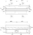
- FIG. 13 is a cross-sectional view of main steps in the gate width direction showing a first conventional method for manufacturing a semiconductor device.
- nMIS shown on the left side indicates an n-type MIS formation region where an n-type MIS transistor is formed
- pMIS shown on the right side indicates a p-type MIS formation where a p-type MIS transistor is formed. Indicates the area.
- the element isolation region 101 is selectively formed on the semiconductor substrate 100.
- the first active region 100a surrounded by the element isolation region 101 is formed in the n-type MIS formation region
- the second active region surrounded by the element isolation region 101 is formed in the p-type MIS formation region.
- 100b is formed.
- the p-type well region 102 a is formed in the n-type MIS formation region in the semiconductor substrate 100
- the n-type well region 102 b is formed in the p-type MIS formation region in the semiconductor substrate 100.
- a gate insulating film forming film a first metal film made of a gate electrode material for an n-type MIS transistor (hereinafter referred to as “nMIS metal material”), and for a p-type MIS transistor
- nMIS metal material a gate electrode material for an n-type MIS transistor
- metal material for pMIS a second metal film made of a gate electrode material and a silicon film
- the first patterning portion 107A is patterned by a dry etching method using a resist having a gate pattern shape formed on the silicon films 106a and 106b as a mask to form the gate insulating film formation film 103a.
- Forming a first gate insulating film and a first gate electrode made of the first metal film 104a, the second metal film 105a, and the silicon film 106a, and patterning the second patterning portion 107B, A second gate insulating film made of the gate insulating film forming film 103b and a second gate electrode made of the second metal film 105b and the silicon film 106b are formed.
- the etching conditions are such that the second gate electrode is formed with high accuracy
- the first metal film 104a and the gate insulating film formation film 103a in the first patterning portion 107A remain without being etched. Therefore, the first gate electrode cannot be formed with high accuracy.
- the etching condition is an etching condition in which the first gate electrode is formed with high accuracy
- etching scraping occurs in the semiconductor substrate 100 and the element isolation region 101 in the p-type MIS formation region. The gate electrode cannot be formed with high accuracy.
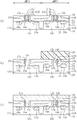
- FIGS. 14A to 14E are cross-sectional views of main steps in the gate width direction showing the second conventional method of manufacturing a semiconductor device in the order of steps.
- nMIS shown on the left side indicates an n-type MIS formation region where an n-type MIS transistor is formed
- pMIS shown on the right side indicates a p-type MIS formation where a p-type MIS transistor is formed. Indicates the area.
- an element isolation region 201 is selectively formed on the semiconductor substrate 200.
- the first active region 200a surrounded by the element isolation region 201 is formed in the n-type MIS formation region
- the second active region surrounded by the element isolation region 201 is formed in the p-type MIS formation region.
- 200b is formed.
- the p-type well region 202 a is formed in the n-type MIS formation region in the semiconductor substrate 200
- the n-type well region 202 b is formed in the p-type MIS formation region in the semiconductor substrate 200.
- the first mask film is etched to form the first mask film 205a, and then the resist mask 206 is removed. Thereafter, the first metal film 204 and the first gate insulating film formation film 203 are sequentially etched using the first mask film 205a as a mask.
- the first gate insulating film formation film 203, the first metal film 204, and the silicon film 211 were sequentially formed on the first active region 200a.
- the second patterning unit in which the first patterning unit is formed and the second gate insulating film forming film 207, the second metal film 208, and the silicon film 211 are sequentially formed on the second active region 200b.
- a resist having a gate pattern shape (not shown) is formed on the silicon film 211 by photolithography, and then the resist is used as a mask and etching is performed by etching.
- the first patterning portion is patterned to form the first gate insulating film 203a, the first gate electrode 212A composed of the first metal film 204a and the first silicon film 211a, and the second patterning portion. Patterning is performed to form a second gate insulating film 207b, and a second gate electrode 212B made of the second metal film 208b and the second silicon film 211b.
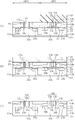
- FIG. 15 is a plan view showing problems in the second conventional method for manufacturing a semiconductor device. Note that the XIVe-XIVe line shown in FIG. 15 corresponds to the cross-sectional line of the cross-sectional view shown in FIG.
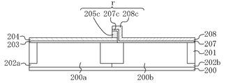
- a resist mask 210 covering the p-type MIS formation region is formed shifted in the gate width direction. As shown in FIG. 14B, the end of the resist mask 210 in the gate width direction is on the n-type MIS formation region side. 14D, the remaining portion 205c of the first mask film 205a, the remaining portion 207c of the second gate insulating film formation film 207, and the second metal film are formed on the element isolation region 201 as shown in FIG. A remaining portion r composed of the remaining portion 208c of 208 is formed to protrude.
- the first and second gate electrodes 212A and 212B are adjacent to the first and second gate electrodes 212A and 212B along the gate length direction. Since it is electrically connected to the first and second gate electrodes (not shown), the first and second gate electrodes 212A and 212B do not function as gate electrodes. Thus, the second conventional method for manufacturing a semiconductor device has a problem that the first and second gate electrodes 212A and 212B cannot be formed.
- the above problem can be avoided by widening the width of the element isolation region 201 in the gate width direction. That is, by providing an alignment margin (margin region) in advance in the element isolation region 201 and increasing the width of the element isolation region 201 in the gate width direction, the resist mask 206 is formed in the step shown in FIG. Even if the resist mask 206 may be formed shifted in the gate width direction, the n-type MIS formation region is not located on the p-type MIS formation region side without positioning the end of the resist mask 206 in the gate width direction. Can be located on the side. At the same time, in the step shown in FIG.
- the end of the resist mask 210 in the gate width direction can be positioned on the p-type MIS formation region side without being positioned on the n-type MIS formation region side.
- this case has the following problems. That is, when forming the resist mask 206 and the resist mask 210, a margin is required for the element isolation region 201. Therefore, the width of the element isolation region 201 in the gate width direction cannot be reduced. There's a problem.
- the first patterning portion and the second patterning portion are different in configuration from each other (in detail).
- the first and second patterning portions have the same silicon film 211, the first and second gate insulating film forming films 203 and 207 and the first and second metal films 204 and 208 are different from each other.
- the etching characteristics are different from each other, patterning is performed under the same etching conditions, so that both the first and second gate electrodes cannot be formed with high accuracy. is there.
- the first conventional semiconductor device manufacturing method has a problem that both the first and second gate electrodes cannot be formed with high accuracy.
- the second conventional method for manufacturing a semiconductor device not only the first and second gate electrodes cannot be formed with high accuracy, but also the width of the element isolation region in the gate width direction is reduced. There is a problem that you can not.
- an object of the present invention is to provide a gate electrode of an n-type and p-type MIS transistor formed with high precision in a semiconductor device having an n-type and p-type MIS transistor having gate electrodes made of different metal materials. It is to realize an element isolation region with a reduced width in the gate width direction.
- a semiconductor device is a semiconductor device including a first MIS transistor and a second MIS transistor, and the first MIS transistor is a first active in a semiconductor substrate.
- an insulating film formed over the upper surface of the region located on the side of the first gate electrode in the active region, and the second MIS transistor is formed on the second active region in the semiconductor substrate.
- a second gate electrode comprising a second gate insulating film, a first metal film formed on the second gate insulating film, and a conductive film formed on the first metal film; 2nd from the side of the gate electrode And an insulating film formed over the upper surface of the region located on the side of the second gate electrode in the active region, and the first metal film and the second metal film are made of different metal materials.
- An insulating film is not formed on each upper surface of the first gate electrode and the second gate electrode.
- the thickness of the insulating film is preferably smaller than the thickness of the first gate electrode.
- the conductive film is made of a silicon film and further includes a metal silicide film formed on the silicon film.
- the first gate insulating film is preferably made of the same insulating material as the second gate insulating film.
- the first gate insulating film is preferably made of an insulating material different from that of the second gate insulating film.
- the cross-sectional shape formed on the side surface of the first gate electrode is an L-shaped first inner side wall and the cross-sectional shape formed on the side surface of the second gate electrode.
- An L-shaped second inner sidewall is further provided, and the insulating film is preferably formed in contact with the first inner sidewall and the second inner sidewall.
- the insulating film is preferably a stress insulating film that generates a first stress in the gate length direction of the channel region in the first active region.
- the driving ability of the first MIS transistor can be improved by applying the first stress in the gate length direction of the channel region in the first active region by the stress insulating film.
- the first MIS transistor is an n-type MIS transistor
- the insulating film is made of a silicon nitride film
- the first stress is a tensile stress.
- the semiconductor device further includes a source / drain region formed outside the second gate electrode in the second active region, and the source / drain region is in a trench provided in the second active region. And a silicon mixed crystal layer that generates a second stress in the gate length direction of the channel region in the second active region.
- the second mixed MIS transistor can improve the driving capability of the second MIS transistor by applying the second stress in the gate length direction of the channel region in the second active region by the silicon mixed crystal layer.
- the second MIS transistor is a p-type MIS transistor
- the silicon mixed crystal layer is a SiGe layer
- the second stress is a compressive stress
- the first gate insulating film and the second gate insulating film include a high dielectric constant film made of a metal oxide having a relative dielectric constant of 10 or more.
- a method of manufacturing a semiconductor device includes a first MIS transistor formed on a first active region in a semiconductor substrate and a second active region in the semiconductor substrate.
- the second gate electrode of the second MIS transistor includes a first metal film in the second gate electrode formation portion.
- the first silicon film and the first gate electrode forming portion in the first gate electrode forming portion are formed.
- a second metal film is formed in a first recess formed by sequentially removing the metal film to form a first gate electrode made of the second metal film.
- a second gate electrode including the first metal film in the second gate electrode formation portion is formed. Therefore, when replacing the first silicon film and the first metal film in the first gate electrode formation portion with the second metal film, a margin is required in accordance with the element isolation region. In the case of the second gate electrode formation portion, no margin is required in accordance with the element isolation region.
- the semiconductor device can be miniaturized.
- the first and second gate electrode forming portions (in other words, the first and second gate electrode forming portions having the same etching characteristics) having the same configuration in the same process
- the first and second gate electrode forming portions can be formed easily and accurately.
- the first metal film and the first silicon film in the first gate electrode forming portion formed with high precision are replaced with the second metal film, and the first gate made of the second metal film is thereby obtained.
- An electrode can be formed.
- the second gate electrode including the first metal film in the second gate electrode formation portion formed with high accuracy can be formed, the first and second gate electrodes formed with high accuracy are realized. can do.
- the step (d) includes a step of forming a first recess in which the first gate insulating film is exposed on the bottom surface on the first active region
- the step (e) Includes a step of forming a second metal film on the first gate insulating film in the first recess, and a step of forming a metal silicide film on the second silicon film after the step (e) ( f), and the second gate electrode is preferably made of the first metal film and the second silicon film in the second gate electrode formation portion.
- a margin is required in accordance with the element isolation region.
- a margin is not required in accordance with the element isolation region, so that the number of processes that require a margin in the element isolation region can be reduced to one.
- the first silicon film, the first metal film, and the first gate insulating film in the first gate electrode formation portion are sequentially removed, Forming a first recess in which the first active region is exposed on the bottom surface on the one active region, and the step (e) forms a third gate insulating film in the first recess; Including a step of forming a second metal film on the third gate insulating film, and further comprising a step (f) of forming a metal silicide film on the second silicon film after the step (e),
- the gate electrode is preferably made of the first metal film and the second silicon film in the second gate electrode formation portion.
- the first inner side having an L-shaped cross section on the side surface of the first gate electrode formation portion Forming a wall, and further forming a second inner sidewall having an L-shaped cross section on the side surface of the second gate electrode forming portion.
- an insulating film is formed The first inner side wall and the second inner side wall are preferably formed in contact with each other.
- a step of forming a trench outside the second gate electrode formation portion in the second active region is further provided.
- (h) and a step (i) of forming a silicon mixed crystal layer that generates stress in the gate length direction of the channel region in the second active region in the trench are further provided.
- the semiconductor device and the manufacturing method thereof after forming the first and second gate electrode forming portions in the same process, the first silicon film and the first gate electrode in the first gate electrode forming portion are formed.
- a second metal film is formed in a first recess formed by sequentially removing the metal film, and a first gate electrode made of the second metal film is formed.
- a second gate electrode including the first metal film in the second gate electrode formation portion is formed. Therefore, when replacing the first silicon film and the first metal film in the first gate electrode formation portion with the second metal film, a margin is required in accordance with the element isolation region. In the case of the second gate electrode formation portion, no margin is required in accordance with the element isolation region.
- the semiconductor device can be miniaturized.
- the first and second gate electrode forming portions having the same configuration are formed in the same process, the first and second gate electrode forming portions can be easily and accurately formed. .
- the first metal film and the first silicon film in the first gate electrode forming portion formed with high precision are replaced with the second metal film, and the first gate made of the second metal film is thereby obtained.
- An electrode can be formed.
- the second gate electrode including the first metal film in the second gate electrode formation portion formed with high accuracy can be formed, the first and second gate electrodes formed with high accuracy are realized. can do.
- FIGS. 1A to 1D are cross-sectional views of relevant steps in the gate length direction showing the method of manufacturing the semiconductor device according to the first embodiment of the present invention in the order of steps.
- 2 (a) to 2 (d) are cross-sectional views of relevant steps in the gate length direction showing the method of manufacturing the semiconductor device according to the first embodiment of the present invention in the order of steps.
- FIGS. 3A to 3D are cross-sectional views of relevant steps in the gate length direction showing the method of manufacturing the semiconductor device according to the first embodiment of the present invention in the order of steps.
- FIGS. 4A to 4C are cross-sectional views of relevant steps in the gate length direction showing the method of manufacturing the semiconductor device according to the first embodiment of the present invention in the order of steps.
- FIGS. 1A to 1D are cross-sectional views of relevant steps in the gate length direction showing the method of manufacturing the semiconductor device according to the first embodiment of the present invention in the order of steps.
- FIGS. 3A to 3D are cross-sectional views of relevant steps in
- FIGS. 5A to 5C are cross-sectional views of relevant steps in the gate length direction showing the method of manufacturing the semiconductor device according to the first embodiment of the present invention in the order of steps.
- FIGS. 6A and 6B are diagrams showing the configuration of the semiconductor device according to the first embodiment of the present invention.
- FIGS. 7A to 7C are cross-sectional views of relevant steps in the gate length direction showing the method of manufacturing the semiconductor device according to the second embodiment of the present invention in the order of steps.
- FIGS. 8A to 8C are cross-sectional views of relevant steps in the gate length direction showing the method of manufacturing the semiconductor device according to the second embodiment of the present invention in the order of steps.
- FIG. 9 is a sectional view in the gate width direction showing the configuration of the semiconductor device according to the second embodiment of the present invention.
- FIGS. 10 (a) to 10 (c) are cross-sectional views of main steps in the gate length direction showing the method of manufacturing the semiconductor device according to the modification of the second embodiment of the present invention in the order of steps.
- FIGS. 11A to 11C are cross-sectional views of relevant steps in the gate length direction showing the method of manufacturing the semiconductor device according to the modification of the second embodiment of the present invention in the order of steps.
- FIG. 12 is a cross-sectional view in the gate width direction showing the configuration of the semiconductor device according to the modification of the second embodiment of the present invention.
- FIG. 13 is a cross-sectional view of main steps in the gate width direction showing a first conventional method for manufacturing a semiconductor device.
- FIG. 14A to 14E are cross-sectional views of main steps in the gate width direction showing the second conventional method of manufacturing a semiconductor device in the order of steps.
- FIG. 15 is a plan view showing problems in the second conventional method for manufacturing a semiconductor device.
- FIG. 16 is a cross-sectional view in the gate width direction showing problems in the second conventional method of manufacturing a semiconductor device.
- FIGS. 1 (a) to 5 (c) are cross-sectional views of essential steps in the gate length direction showing the method of manufacturing the semiconductor device according to the first embodiment of the present invention in the order of steps.
- nMIS shown on the left side indicates an n-type MIS formation region where an n-type MIS transistor is formed
- pMIS shown on the right side indicates a p-type MIS formation where a p-type MIS transistor is formed. Indicates the area.
- element isolation in which an insulating film is embedded in a trench on a semiconductor substrate 10 made of, for example, p-type silicon by, for example, a buried element isolation (STI) method.
- the region 11 is selectively formed.
- the first active region 10 a made of the semiconductor substrate 10 surrounded by the element isolation region 11 is formed in the n-type MIS formation region, and the p-type MIS formation region is surrounded by the element isolation region 11.
- a second active region 10b made of the semiconductor substrate 10 is formed.
- a p-type impurity such as B (boron), for example, is implanted into the n-type MIS formation region in the semiconductor substrate 10 by lithography and ion implantation, while P (for example) is introduced into the p-type MIS formation region in the semiconductor substrate 10.
- P for example
- the semiconductor substrate 10 is subjected to a heat treatment at 850 ° C. for 30 seconds, for example, to form a p-type well region 12a in the n-type MIS formation region in the semiconductor substrate 10.
- an n-type well region 12 b is formed in the p-type MIS formation region in the semiconductor substrate 10.
- the first metal film 14 in addition to the TiN film, for example, a metal such as titanium (Ti), ruthenium (Ru), platinum (Pt), or tungsten (W), or Ti, Ru, Nitride, carbon nitride, or silicon nitride containing at least one metal of Pt and W can be used.
- a silicon film 15 made of, for example, a polysilicon film having a thickness of 100 nm, for example, is deposited on the first metal film 14 by, for example, a CVD method, and then, for example, a film thickness of, for example, on the silicon film 15 is, for example, A protective film 16 made of a 30 nm silicon oxide film is deposited.
- a resist (not shown) having a gate pattern shape is formed on the protective film 16 by photolithography.
- the protective film 16, the silicon film 15, the first metal film 14, and the gate insulating film forming film 13 are sequentially patterned by a dry etching method using the resist as a mask.
- the first gate insulating film 13a, the first metal film 14a, the first silicon film 15a, and the first protective film 16a are sequentially formed on the first active region 10a, and the second active region 10a is formed.
- a second gate insulating film 13b, a first metal film 14b, a second silicon film 15b, and a second protective film 16b are sequentially formed on the region 10b.
- the first gate electrode forming portion 14A having the first gate insulating film 13a, the first metal film 14a, and the first silicon film 15a is formed on the first active region 10a
- the first A second gate electrode formation portion 14B having a second gate insulating film 13b, a first metal film 14b, and a second silicon film 15b is formed on the second active region 10b.
- the offset spacer Anisotropic etching is performed on the insulating film.
- the first offset spacer 17a is formed on the side surface of the first gate electrode forming portion 14A
- the second offset spacer 17b is formed on the side surface of the second gate electrode forming portion 14B.
- the first gate electrode formation portion 14A is formed in the first active region 10a.
- an n-type impurity such as As (arsenic) as a mask
- an n-type source having a relatively shallow junction depth is formed laterally below the first gate electrode formation portion 14A in the first active region 10a.
- a drain region (LDD region or extension region) 18a is formed in a self-aligning manner.
- the second gate electrode formation portion 14B is formed in the second active region 10b.
- a p-type impurity such as BF 2 as a mask
- a p-type source / drain region having a relatively shallow junction depth is formed laterally below the second gate electrode forming portion 14B in the second active region 10b.
- (LDD region or extension region) 18b is formed in a self-aligned manner.
- a first insulating film made of a silicon oxide film having a thickness of 10 nm and a silicon film having a thickness of 30 nm are formed on the entire surface of the semiconductor substrate 10 by, eg, CVD.
- a second insulating film made of a nitride film anisotropic etching is performed on the first insulating film and the second insulating film.
- the first inner side wall 19a made of the first insulating film having the L-shaped cross section and the first side wall are formed on the side surface of the first gate electrode forming portion 14A via the first offset spacer 17a.
- the first side wall 20A composed of the first outer side wall 20a made of the second insulating film formed on the inner side wall 19a is formed, and the side surface of the second gate electrode forming portion 14B is formed.
- a second inner side wall 19b made of a first insulating film having an L-shaped cross section and a second inner side wall 19b formed on the second inner side wall 19b via a second offset spacer 17b.
- a second sidewall 20B composed of a second outer sidewall 20b made of an insulating film is formed.
- a surface protective film 21 made of, for example, a silicon oxide film having a thickness of 10 nm is deposited on the entire surface of the semiconductor substrate 10 by, eg, CVD.
- a resist mask 22 that covers the n-type MIS formation region and opens the p-type MIS formation region is formed on the surface protective film 21, and then the second outer sidewall 20b.
- the surface protection film 21a formed in the p-type MIS formation region is removed using an anisotropic dry etching method having a selection ratio with respect to (silicon nitride film), and the surface protection film 21a is formed in the n-type MIS formation region. Remain.
- a region outside the second sidewall 20B in the second active region 10b, that is, the surface of the source / drain formation region is exposed.
- the surface protective film 21a (silicon oxide film), the second protective film 16b (silicon oxide film), and the second offset spacer 17b ( The silicon oxide film), the second inner side wall 19b (silicon oxide film), and the second outer side wall 20b (silicon nitride film) are used in a dry etching method having a selective ratio, or have a selective ratio to these films.
- the second active region 10b exposed on the surface is etched using a dry etching method and a wet etching method in combination.
- the first active region 10a is not etched.
- the upper surface of the first silicon film 15a is sequentially covered with the first protective film 16a and the surface protective film 21a, while the upper surface of the second silicon film 15b is covered with the second protective film 16b. Therefore, the first and second silicon films 15a and 15b are not etched.
- etching residues and natural oxide film in the trench 23 by, for example, hydrofluoric acid treatment, for example, by CVD, for example, silane gas (SiH 4 ) and germane gas ( By supplying GeH 4 ) together with a p-type dopant gas such as diborane gas (B 2 H 6 ) at a temperature of, for example, 650 to 700 ° C., a silicon mixed crystal composed of a p-type SiGe layer so as to fill the trench 23 Layer 24 is grown epitaxially.
- the SiGe layer is not epitaxially grown on the first active region 10a.
- the upper surface of the first silicon film 15a is sequentially covered with the first protective film 16a and the surface protective film 21a, while the upper surface of the second silicon film 15b is covered with the second protective film 16b. Therefore, the SiGe layer is not epitaxially grown on the first and second silicon films 15a and 15b.
- a dry etching method having a selection ratio with the semiconductor substrate 10 and the first outer sidewall 20a (silicon nitride film) is used, or a dry etching method and a wet etching method having a selection ratio with these films are sequentially used in combination.
- the surface protective film 21a formed in the n-type MIS formation region is removed, and the region under the first sidewall 20A in the first active region 10a, that is, the surface of the source / drain formation region is removed. Expose.
- the second active region 10b has a trench 23 formed on the outer side of the second sidewall 20B.
- a silicon mixed crystal layer 24 that generates compressive stress in the gate length direction of the channel region in the second active region 10b is formed.
- a first gate electrode forming portion 14A, a first offset spacer 17a, and a first sidewall are formed in the first active region 10a by lithography and ion implantation.
- 20A as a mask and implanting an n-type impurity such as As (arsenic), for example, the outer side of the first sidewall 20A in the first active region 10a is lower than the shallow n-type source / drain region 18a.
- An n-type source / drain region 25a having a deep junction depth and a relatively deep junction depth is formed in a self-aligned manner.
- a p-type impurity such as B (boron), for example, is implanted into the second active region 10b using the second gate electrode forming portion 14B, the second offset spacer 17b, and the second sidewall 20B as a mask.
- B boron
- the p-type source / drain having a junction depth deeper than the shallow p-type source / drain region 18b and relatively deep in the second active region 10b outside the second sidewall 20B.
- the region 25b is formed in a self-aligning manner. Thereafter, the impurities contained in the deep n-type source / drain region 25a and the deep p-type source / drain region 25b are activated by heat treatment.
- the deep p-type source / drain region 25b is formed to include the silicon mixed crystal layer 24 formed in the trench 23 provided in the second active region 10b.
- the entire surface of the semiconductor substrate 10 is formed by, for example, sputtering.
- a metal film (not shown) made of nickel having a thickness of 10 nm is deposited.
- Si in the deep n-type source / drain region 25a and the deep p-type source / drain region 25b is reacted with Ni in the metal film by, for example, a first RTA (Rapid Thermal Annealing) process at 320 ° C. in a nitrogen atmosphere.
- first and second metal silicide films 26a and 26b made of nickel silicide are formed on the deep n-type source / drain region 25a and the deep p-type source / drain region 25b.
- the semiconductor substrate 10 is immersed in an etching solution made of a mixed solution of sulfuric acid and hydrogen peroxide solution, whereby the element isolation region 11, the first and second offset spacers 17a and 17b, and the first and second regions.
- the first RTA treatment is performed at a temperature higher than the temperature at the first RTA treatment (for example, 550 ° C.) by the second RTA treatment.
- the silicide composition ratio of the second metal silicide films 26a and 26b is stabilized.
- the first outer sidewall is formed by using a dry etching method having a selection ratio with respect to the first and second inner sidewalls 19a and 19b (silicon oxide film). 20a (silicon nitride film) and second outer side wall 20b (silicon nitride film) are removed.
- an insulating film 27 made of a silicon nitride film of, eg, a 50 nm-thickness is deposited on the entire surface of the semiconductor substrate 10 by, eg, plasma CVD.
- the insulating film 27 includes the first gate electrode forming portion 14A having the first protective film 16a formed on the surface and the second gate electrode forming portion having the second protective film 16b formed on the surface. It is formed so as to cover 14B.
- the insulating film 27 has an L-shaped cross-sectional shape from which the first outer side wall 20a is removed and the first inner side wall 19a having the L-shaped cross-sectional shape and the second outer side wall 20b is removed. It is formed in contact with the second inner side wall 19b.
- a first interlayer insulating film 28 made of a silicon oxide film is deposited on the insulating film 27 by, eg, CVD, and then the surface of the first interlayer insulating film 28 is formed by, eg, CMP (Chemical—Mechanical—Polishing). While planarizing, the first interlayer insulating film 28 is removed by polishing until the upper surface of the insulating film 27 formed on the first protective film 16a and the second protective film 16b is exposed.
- the first gate electrode is formed using a dry etching method or a wet etching method having a selection ratio with respect to the first and second silicon films (polysilicon films) 15a and 15b.
- the first and second protective films (silicon oxide films) 16a and 16b and the insulating film (silicon nitride film) 27 formed on the formation part 14A and the second gate electrode formation part 14B are removed, The top surfaces of the first silicon film 15a in the first gate electrode formation portion 14A and the second silicon film 15b in the second gate electrode formation portion 14B are exposed.
- the insulating film 27 is formed on the side surfaces of the first and second gate electrode formation portions 14A and 14B from the first and second gate electrode formation portions 14A and 14b in the first and second active regions 10a and 10b. While formed over the upper surface of the region located on the side of 14B, it is not formed on the upper surfaces of the first and second gate electrode forming portions 14A and 14B.
- the first silicon film 15a and the first silicon film 15a in the first gate electrode formation portion 14A are formed by using a dry etching method or a wet etching method having a selection ratio with respect to 19a, 19b, the insulating film 27, and the first interlayer insulating film 28.
- the second silicon film 15b in the second gate electrode formation portion 14B is removed.
- the first gate insulating film 13a, The first offset spacer 17a, the first inner sidewall 19a, the insulating film 27, and the first interlayer insulating film 28 are used in the first gate electrode formation portion 14A in the first gate electrode formation portion 14A by using a wet etching method having a selection ratio.
- the metal film 14a is removed.
- the first silicon film 15a and the first metal film 14a in the first gate electrode formation portion 14A are sequentially removed by sequentially performing the steps shown in FIGS.
- a first recess Ca that is surrounded by an insulating film 27 through a first offset spacer 17a and a first inner side wall 19a in order, and the first gate insulating film 13a is exposed on the bottom surface.
- the second silicon film 15b in the second gate electrode formation portion 14B is removed through the process shown in FIG. 4B, and the second offset spacer is formed on the second active region 10b.
- a second recess Cb is formed, which is surrounded by the insulating film 27 via the 17b and the second inner side wall 19b in order, and the first metal film 14b is exposed on the bottom surface.
- the second metal film 30 include, for example, a metal such as tantalum (Ta) or hafnium (Hf) in addition to TaN, or a nitride or carbon nitride containing at least one of Ta and Hf. Or a silicon nitride etc. are mentioned.
- a metal such as tantalum (Ta) or hafnium (Hf) in addition to TaN, or a nitride or carbon nitride containing at least one of Ta and Hf. Or a silicon nitride etc. are mentioned.
- the second metal film 30 is removed by, for example, CMP or etchback until the upper surface of the insulating film 27 is exposed.
- the second metal film 30a is formed on the first gate insulating film 13a in the first recess Ca, and the second metal film is formed on the first metal film 14b in the second recess Cb. 30b is formed.
- the first gate electrode 30A made of the second metal film 30a is formed on the first active region 10a via the first gate insulating film 13a, while the second active region 10b.
- a second gate electrode 30B composed of the first metal film 14b and the second metal film 30b is formed thereon via the second gate insulating film 13b.
- the second interlayer insulating film is formed on the first interlayer insulating film 28 so as to cover the first and second gate electrodes 30A and 30B by, for example, the CVD method.
- the surface of the second interlayer insulating film 31 is planarized by, eg, CMP.
- a resist (not shown) is formed on the second interlayer insulating film 31 in the same manner as in the method of manufacturing a semiconductor device having a normal MIS transistor, and then the insulating is performed by dry etching using the resist as a mask.
- First and second contact holes 32a and 32b reaching the upper surfaces of the first and second metal silicide films 26a and 26b are formed in the film 27, the first interlayer insulating film 28, and the second interlayer insulating film 31, respectively. Form.
- the amount of overetching of the first and second metal silicide films 26a and 26b can be reduced by using a two-step etching method in which etching is once stopped when the insulating film 27 is exposed.
- the semiconductor device according to the present embodiment that is, the n-type MIS transistor NTr having the first gate electrode 30A made of the second metal film 30a, the first metal film 14b, and the second metal A semiconductor device including the p-type MIS transistor PTr having the second gate electrode 30B made of the film (conductive film) 30b can be manufactured.
- 6A and 6B are diagrams showing the configuration of the semiconductor device according to the first embodiment of the present invention.
- FIG. 6A is a plan view
- FIG. FIG. 6B is a cross-sectional view in the gate width direction along the line VIb-VIb shown in FIG.
- the Vl-Vl line shown in FIG. 6 (a) a corresponds to the cross-sectional line in the left figure in FIG. 5 (c) c
- the Vr-Vr line shown in FIG. 6 (a) is shown in FIG. 5 (c). It corresponds to the cross-sectional line in the right figure.
- nMIS shown on the left side indicates an n-type MIS formation region where an n-type MIS transistor is formed
- pMIS shown on the right side indicates a p-type MIS formation where a p-type MIS transistor is formed. Indicates the area.
- the first active region 10a surrounded by the element isolation region is formed in the n-type MIS formation region, and the p-type MIS formation region is surrounded by the element isolation region.
- a second active region 10b is formed.
- a first gate electrode 30A is formed on the first active region 10a via a first gate insulating film, and a second gate insulating film is formed on the second active region 10b.
- a second gate electrode 30B is formed.
- An insulating film 27 is formed on the side surfaces of the first and second gate electrodes 30A and 30B through the first and second offset spacers 17a and 17b and the first and second inner side walls 19a and 19b in this order. Is formed.
- FIG. 6A the first active region 10a surrounded by the element isolation region is formed in the n-type MIS formation region, and the p-type MIS formation region is surrounded by the element isolation region.
- a second active region 10b is formed.
- a first gate electrode 30A is formed on the first active region 10
- an element isolation region 11 in which an insulating film is embedded in a trench is formed above the semiconductor substrate 10 so as to partition the n-type MIS formation region and the p-type MIS formation region. Is formed.
- a p-type well region 12 a is formed in the n-type MIS formation region of the semiconductor substrate 10, while an n-type well region 12 b is formed in the p-type MIS formation region of the semiconductor substrate 10.
- a first gate electrode 30A made of a second metal film 30a is formed on the first active region 10a via a first gate insulating film 13a, while the first gate electrode 30A is formed on the second active region 10b.
- the n-type MIS transistor NTr includes a first active region 10a surrounded by the element isolation region 11 in the semiconductor substrate 10, and a first active region 10a formed on the first active region 10a.
- Gate insulating film 13a, first gate electrode 30A made of second metal film 30a formed on first gate insulating film 13a, and first offset spacer on the side surface of first gate electrode 30A A first inner side wall 19a having an L-shaped cross section formed through 17a, and a shallow n-type source / drain region 18a formed laterally below the first gate electrode 30A in the first active region 10a.
- the p-type MIS transistor PTr includes a second active region 10b surrounded by the element isolation region 11 in the semiconductor substrate 10 and a second active region 10b formed on the second active region 10b.
- the second metal film 30a constituting the first gate electrode 30A is made of a metal material (or metal compound material) having a work function of 4.05 eV or more and 4.6 eV or less, while the second gate electrode 30B is made of
- the first metal film 14b to be formed is made of a metal material (or metal compound material) having a work function of 4.6 eV or more and 5.15 eV or less.
- the second metal film 30a and the first metal film 14b have different work functions and are made of different metal materials (or metal compound materials).
- the first gate electrode 30A and the second gate electrode 30B have the same top surface height, and the first gate electrode 30A is made of the second metal film 30a, while the second gate electrode
- the electrode 30B includes a first metal film 14b and a second metal film 30b. Therefore, the film thickness of the second metal film 30a is thicker than the film thickness of the first metal film 14b and the film thickness of the second metal film (conductive film) 30b.
- the insulating film 27 is a region located on the side of the first and second gate electrodes 30A and 30B and on the side of the first and second gate electrodes 30A and 30B in the first and second active regions 10a and 10b. On the other hand, it is not formed on the upper surfaces of the first and second gate electrodes 30A and 30B. The insulating film 27 is thinner than the first and second gate electrodes 30A and 30B.
- the first gate insulating film 13a and the second gate insulating film 13b are formed in the same process and are made of the same insulating material.
- the first gate electrode forming portion 14A has the first A second metal film 30a is formed in a first concave portion Ca (see FIG. 4C) formed by sequentially removing the silicon film 15a and the first metal film 14a, thereby forming a second metal film.
- a first gate electrode 30A made of 30a is formed.
- a second metal film 30b is formed in a second recess Cb (see FIG. 4B) formed by removing the second silicon film 15b in the second gate electrode formation portion 14B.
- a second gate electrode 30B see FIG.
- a margin is required for the element isolation region 201 when forming the resist mask 206 in the step shown in FIG. (b) Since the alignment margin is required for the element isolation region 201 when the resist mask 210 is formed in the step (b), there are two alignment margin required steps. The width in the gate width direction cannot be reduced.
- the same silicon film 15, the same first metal film 14, and the same gate insulating film forming film 13 are sequentially patterned, Since the first and second gate electrode forming portions 14A and 14B are formed, the first and second gate electrode forming portions 14A and 14B can be easily and accurately formed. Thereby, the first metal film 14a and the first silicon film 15a in the first gate electrode formation portion 14A formed with high accuracy are replaced with the second metal film 30a, and the second metal film 30a is used.
- the first gate electrode 30A While forming the first gate electrode 30A, the second metal film 15b in the second gate electrode formation portion 14B formed with high precision is replaced with the second metal film 30b, and the first metal film Since the second gate electrode 30B made of 14b and the second metal film 30b can be formed, the first and second gate electrodes 30A and 30B formed with high precision can be realized.
- the first patterning portion 107A and the second patterning portion 107B are identical to each other even though their configurations are different from each other. Since the patterning is performed in this step, as described above, both the first and second gate electrodes cannot be formed with high accuracy.
- the second conventional method of manufacturing a semiconductor device as shown in FIG. 14D, the first patterning portion and the second patterning portion are identical to each other even though their configurations are different from each other. Since the patterning is performed in this step, as described above, both the first and second gate electrodes cannot be formed with high accuracy.
- the deep p-type source / drain region 25b includes the silicon mixed crystal layer 24 that generates compressive stress in the gate length direction of the channel region in the second active region 10b, so that the channel region in the second active region 10b Since compressive stress can be applied in the gate length direction, the driving capability of the p-type MIS transistor can be improved.
- a deep n is formed after the formation of the first and second sidewalls 20A and 20B (see FIG. 2A) for the purpose of improving the driving capability of the p-type MIS transistor.
- the steps shown in FIG. 2B to FIG. 3A are sequentially performed to obtain the second active region 10b.
- the silicon mixed crystal layer 24 made of, for example, a p-type SiGe layer is formed in the trench 23 formed on the outer side of the side wall 20B of the present invention has been described as a specific example. However, the present invention is not limited to this. It is not something.
- the steps shown in FIG. 2B to FIG. 3A are not performed sequentially, that is, Without forming the silicon mixed crystal layer 24, deep n-type and p-type source / drain regions 25a and 25b may be formed as shown in FIG.
- a silicon mixed crystal layer that generates tensile stress in the gate length direction of the channel region in the first active region 10a in the trench formed outside the first sidewall 20A in the first active region 10a. (For example, an n-type SiC layer) may be formed. In this case, it is possible to improve the driving capability of the n-type MIS transistor instead of the p-type MIS transistor.
- a semiconductor device and a manufacturing method thereof according to a second embodiment of the present invention will be described with reference to the drawings.
- the semiconductor device and the manufacturing method thereof according to the second embodiment will be described mainly with respect to the differences from the semiconductor device according to the first embodiment and the manufacturing method thereof, and common points will be omitted as appropriate. I will explain.
- FIGS. 7A to 8C are cross-sectional views of essential steps in the gate length direction showing the method of manufacturing the semiconductor device according to the second embodiment of the present invention in the order of steps.
- FIGS. 7 (a) to 8 (c) the same constituent elements as those in the first embodiment described above are shown in FIGS. 1 (a) to 5 (c) in the first embodiment.
- nMIS shown on the left side indicates an n-type MIS formation region where an n-type MIS transistor is formed
- pMIS shown on the right side indicates a p-type MIS formation where a p-type MIS transistor is formed. Indicates the area.
- the first metal film 14a, The first gate electrode forming portion 14A is formed by using a dry etching method or a wet etching method having a selection ratio with the one offset spacer 17a, the first inner side wall 19a, the insulating film 27, and the first interlayer insulating film 28.
- the first silicon film 15a is removed.
- the first gate insulating film 13a, the first offset spacer 17a, the first inner side wall 19a, the insulating film 27, and the first interlayer insulating film 28 are used to form the first etching.
- the first metal film 14a in the first gate electrode formation portion 14A is removed.
- a first recess Ca is formed which is surrounded by the insulating film 27 sequentially through one inner side wall 19a and exposes the first gate insulating film 13a on the bottom surface.
- the first recess Ca is embedded on the semiconductor substrate 10 by, for example, CVD, ALD, or sputtering.
- a second metal film 30 made of TaN is deposited.
- the second metal film 30 is removed by, for example, a CMP method or an etch back method until the upper surface of the insulating film 27 is exposed. Thereby, the second metal film 30a is formed on the first gate insulating film 13a in the first recess Ca.
- the first gate electrode 30A made of the second metal film 30a is formed on the first active region 10a via the first gate insulating film 13a, while the second active region 10b.
- a second gate electrode 30B made of the first metal film 14b and the second silicon film 15b is formed thereon via the second gate insulating film 13b.
- the entire surface of the semiconductor substrate 10 is formed by, for example, sputtering.
- a metal film (not shown) made of nickel having a thickness of 10 nm is deposited.
- the Si of the second silicon film 15b is reacted with the Ni of the metal film by a first RTA process in a nitrogen atmosphere at 320 ° C., for example, and nickel silicide is formed on the upper part of the second silicon film 15b.
- a metal silicide film 34 made of is formed.
- the temperature is higher than the temperature in the first RTA process (for example, 550 ° C.),
- the silicide composition ratio of the metal silicide film 34 is stabilized by the second RTA process.
- the second interlayer insulating film is formed on the first interlayer insulating film 28 so as to cover the first and second gate electrodes 30A and 30B by, for example, the CVD method.
- the surface of the second interlayer insulating film 31 is planarized by, eg, CMP.
- the first and second contact holes 32 a and 32 b in the insulating film 27, the first interlayer insulating film 28, and the second interlayer insulating film 31 are made in the same manner as in the method of manufacturing a semiconductor device having a normal MIS transistor.
- the first and second contact plugs 33a and 33b are formed, and are connected to the first and second metal silicide films 26a and 26b.
- metal wiring (not shown) that is electrically connected to the first and second contact plugs 33 a and 33 b is formed on the second interlayer insulating film 31.
- the semiconductor device according to the present embodiment that is, the n-type MIS transistor NTr having the first gate electrode 30A made of the second metal film 30a, the first metal film 14b, and the second silicon
- a semiconductor device including the p-type MIS transistor PTr having the second gate electrode 30B made of the film (conductive film) 15b can be manufactured.
- the difference in the manufacturing method between the present embodiment and the first embodiment is as follows.
- the second recess Cb formed by removing the second silicon film 15b in the second gate electrode formation portion 14B has the second recess Cb.
- the metal film 30b is formed, and the second gate electrode 30B including the first metal film 14b and the second metal film 30b in the second gate electrode formation portion 14B is formed.
- the second gate electrode is formed without removing the second silicon film 15b in the second gate electrode formation portion 14B.
- a second gate electrode 30B made of the first metal film 14b and the second silicon film 15b in the formation portion 14B is formed.
- a metal silicide film 34 is formed on the second silicon film 15b in the second gate electrode 30B.
- FIG. 9 is a sectional view in the gate width direction showing the configuration of the semiconductor device according to the second embodiment of the present invention.
- the same components as those in the first embodiment are denoted by the same reference numerals as those shown in FIG. 6 (b) in the first embodiment.
- nMIS shown on the left side indicates an n-type MIS formation region where an n-type MIS transistor is formed
- pMIS shown on the right side indicates a p-type MIS formation where a p-type MIS transistor is formed. Indicates the area.
- the first gate electrode 30A made of the second metal film 30a is formed on the first active region 10a via the first gate insulating film 13a.
- the second active region 10b includes a first metal film 14b and a second silicon film (conductive film) 15b formed on the first metal film 14b via a second gate insulating film 13b.
- a second gate electrode 30B is formed.
- a metal silicide film 34 is formed on the second silicon film 15b.
- the second gate electrode 30B is composed of the first metal film 14b and the second silicon film 15b.
- a metal silicide film 34 is formed on the second silicon film 15b.
- the second gate electrode 30B includes the first metal film 14b and the second metal film 30b.
- the conductive film formed on the first metal film 14b in the second gate electrode 30B is the second silicon film 15b in the present embodiment, whereas the second conductive film in the first embodiment is the second film.
- the metal film 30b is the metal film 30b.
- the first gate electrode forming portion 14A has the first A second metal film 30a is formed in a first recess Ca (see FIG. 7B) formed by sequentially removing the silicon film 15a and the first metal film 14a.
- a first gate electrode 30A made of 30a is formed.
- the second gate electrode 30B composed of the first metal film 14b and the second silicon film 15b in the second gate electrode formation portion 14B is formed. Therefore, when removing the first silicon film 15a and the first metal film 14a in the first gate electrode formation portion 14A, as shown in FIG.
- the n-type MIS formation region and the p-type MIS are removed.
- a margin is required in accordance with the element isolation region 11, but the first and second gate electrode formation portions 14A and 14B are formed.
- no margin is required for the element isolation region 11. Therefore, since the number of alignment margin steps can be reduced to one, the width of the element isolation region 11 in the gate width direction (see FIG. 9: Wnp) can be reduced, so that the semiconductor device can be miniaturized. be able to.
- the same silicon film 15, the same first metal film 14, and the same gate insulating film forming film 13 are sequentially patterned, Since the first and second gate electrode forming portions 14A and 14B are formed, the first and second gate electrode forming portions 14A and 14B can be easily and accurately formed. Thereby, the first metal film 14a and the first silicon film 15a in the first gate electrode formation portion 14A formed with high accuracy are replaced with the second metal film 30a, and the second metal film 30a is used.
- the first gate electrode 30A is formed, while the second gate electrode 30B composed of the first metal film 14b and the second silicon film 15b in the second gate electrode formation portion 14B formed with high precision is formed. Therefore, the first and second gate electrodes 30A and 30B formed with high accuracy can be realized.
- the deep p-type source / drain region 25b includes the silicon mixed crystal layer 24, so that compressive stress can be applied in the gate length direction of the channel region in the second active region 10b. Therefore, the driving capability of the p-type MIS transistor can be improved.
- nMIS shown on the left side indicates an n-type MIS formation region where an n-type MIS transistor is formed
- pMIS shown on the right side indicates a p-type MIS formation where a p-type MIS transistor is formed. Indicates the area.
- the steps shown in FIGS. 1 (a) to 4 (a) in the first embodiment are sequentially performed, and the configuration shown in FIG. 7 (a) is obtained as in the second embodiment.
- the gate insulating film forming film 13 in this modification has an optimized film thickness for the p-type MIS transistor and is made of an insulating material optimized for the p-type MIS transistor.
- the first metal film 14a, The first gate electrode forming portion 14A is formed by using a dry etching method or a wet etching method having a selection ratio with the one offset spacer 17a, the first inner side wall 19a, the insulating film 27, and the first interlayer insulating film 28.
- the first silicon film 15a is removed.
- the first gate insulating film 13a, the first offset spacer 17a, the first inner side wall 19a, the insulating film 27, and the first interlayer insulating film 28 are used to form the first etching.
- the first metal film 14a in the first gate electrode formation portion 14A is removed.
- the same process as the process shown in FIG. 7B in the second embodiment is performed.
- the first gate insulating film 13a in the first gate electrode formation portion 14A is removed using a wet etching method having a selection ratio with the semiconductor substrate.
- first silicon film 15a, the first metal film 14a, and the first gate insulating film 13a in the first gate electrode formation portion 14A are sequentially removed to form the first active region 10a on the first active region 10a.
- a first recess Ca is formed, which is surrounded by the insulating film 27 through the first offset spacer 17a and the first inner side wall 19a in order, and the first active region 10a is exposed to the bottom surface.
- a chemical oxide film (not shown) is formed on the surface of the semiconductor substrate 10 by, for example, HPM (Hydrochloric Acid / Hydrogen Peroxide / Water Mixture) treatment.
- HPM Hydrogen Peroxide / Water Mixture
- a gate insulating film forming film 35 made of a high dielectric constant film having a film thickness of, for example, 2 nm is deposited on the semiconductor substrate 10 by, eg, MOCVD so as to cover the inside of the first recess Ca.
- the gate insulating film forming film 35 desirably includes a high dielectric constant film made of a metal oxide having a relative dielectric constant of 10 or more.
- the gate insulating film forming film 35 has a film thickness optimized for the n-type MIS transistor and is made of an insulating material optimized for the n-type MIS transistor.
- a second metal film made of, for example, TaN is embedded on the semiconductor substrate 10 by, for example, CVD, ALD, or sputtering so as to fill the first recess Ca through the gate insulating film forming film 35. 30 is deposited.
- the second metal film 30 and the gate insulating film forming film 35 are removed until the upper surface of the insulating film 27 is exposed by, for example, a CMP method or an etch back method.
- the third gate insulating film 35a is formed in the first recess Ca, and the second metal film 30a is formed on the third gate insulating film 35a.
- the third gate insulating film 35a is formed from the first active region 10a to the side surface of the second metal film 30a in the first recess Ca. Therefore, although the figure shown in FIG.
- the third gate insulating film 35a includes the second metal film 30a adjacent to each other along the gate width direction. It is formed so as to be interposed between the first metal film 14b and the second silicon film 15b.
- the upper portion of the third gate insulating film 35a is removed by an etching method having a selection ratio with the second metal film 30a or by, for example, dilute hydrofluoric acid treatment.
- the upper end height of the third gate insulating film 35a is made lower than the upper surface height of the second metal film 30a to form the trench R.
- the trench R is formed along the periphery of the second metal film 30a so as to expose the side surface of the second metal film 30a. Therefore, the figure shown in FIG. 11 (a) is not shown because it is a cross-sectional view in the gate length direction, but the trench R has the second metal film 30a and the second silicon film adjacent to each other along the gate width direction. 15b, and the side surface in the gate width direction of the second metal film 30a and the side surface in the gate width direction of the second silicon film 15b are exposed in the trench R.
- the third gate insulating film 35a is formed in the first recess Ca, and the third gate insulating film 35a is formed on the third gate insulating film 35a. Then, the second metal film 30a whose side surface is exposed in the groove R is formed.
- the first gate electrode 30A made of the second metal film 30a is formed on the first active region 10a via the third gate insulating film 35a, while the second active region 10b.
- a second gate electrode 30B made of the first metal film 14b and the second silicon film 15b is formed thereon via the second gate insulating film 13b.
- the entire surface of the semiconductor substrate 10 is formed by, for example, sputtering.
- a metal film (not shown) made of nickel having a thickness of 10 nm is deposited.
- the Si of the second silicon film 15b is reacted with the Ni of the metal film by a first RTA process in a nitrogen atmosphere at 320 ° C., for example, and nickel silicide is formed on the upper part of the second silicon film 15b.
- a metal silicide film 34 made of is formed.
- the metal silicide film 34 in this modification is also formed in the trench R formed between the second metal film 30a and the second silicon film 15b due to the volume expansion thereof. That is, it is formed in contact with the side surface in the gate width direction of the second metal film 30a exposed in the trench R and the side surface in the gate width direction of the second silicon film 15b (see FIG. 12: 34 described later). . Therefore, the second metal film 30a and the second silicon film 15b can be electrically connected by the metal silicide film 34.
- the temperature is higher than the temperature in the first RTA process (for example, 550 ° C.),
- the silicide composition ratio of the metal silicide film 34 is stabilized by the second RTA process.
- the semiconductor device according to the present embodiment that is, the n-type MIS transistor NTr having the first gate electrode 30A made of the second metal film 30a, the first metal film 14b, and the second silicon
- a semiconductor device including the p-type MIS transistor PTr having the second gate electrode 30B made of the film (conductive film) 15b can be manufactured.
- the first gate insulating film 13a is removed in addition to the first silicon film 15a and the first metal film 14a in the first gate electrode formation portion 14A.
- a third gate insulating film 35a is formed in the concave portion Ca (see FIG. 10A), and a second metal film 30a is formed on the third gate insulating film 35a.
- the first gate insulating film 13a in the first gate electrode formation portion 14A is replaced with the third gate insulating film 35a, and the first adjacent to each other along the gate width direction.
- a third gate insulating film 35a is interposed between the gate electrode 30A and the second gate electrode 30B. Therefore, in this modification, for the purpose of achieving electrical connection between the first gate electrode 30A and the second gate electrode 30B when the metal silicide film 34 (see FIG. 11B) is formed.
- the upper portion of the third gate insulating film 35a is removed to form a groove R, and the side surface of the second metal film 30a in the gate width direction and the second metal film 30a are formed in the groove R.
- the side surface of the silicon film 15b in the gate width direction is exposed. 11B is not shown because it is a cross-sectional view in the gate length direction, but the metal silicide film 34 is exposed in the trench R as shown in FIG. Since the metal film 30a can be formed on the side surface in the gate width direction of the metal film 30a and the side surface in the gate width direction of the second silicon film 15b, the second metal film 30a and the second silicon film 15b are electrically connected. Thus, the first gate electrode 30A and the second gate electrode 30B can be electrically connected.
- FIG. 12 is a cross-sectional view in the gate width direction showing the configuration of the semiconductor device according to the modification of the second embodiment of the present invention.
- the same components as those in the second embodiment are denoted by the same reference numerals as those shown in FIG. 9 in the second embodiment.
- “nMIS” shown on the left side indicates an n-type MIS formation region where an n-type MIS transistor is formed
- “pMIS” shown on the right side indicates a p-type MIS formation where a p-type MIS transistor is formed. Indicates the area.
- the first gate electrode 30A made of the second metal film 30a is formed via the third gate insulating film 35a.
- the second active region 10b includes a first metal film 14b and a second silicon film (conductive film) 15b formed on the first metal film 14b via a second gate insulating film 13b.
- a second gate electrode 30B is formed.
- a metal silicide film 34 is formed on the second silicon film 15b.
- the third gate insulating film 35a is made of an insulating material different from that of the second gate insulating film 13b. Then, as shown in FIG. 12, the third gate insulating film 35a is formed from the first active region 10a to the side surface in the gate width direction of the second metal film 30a. It is interposed between the lower region of 30A and the lower region of the second gate electrode 30B (Note that the third gate insulating film 35a is formed of the second metal film 30a as shown in FIG. 11C). In the gate width direction as well as on the side surface in the gate length direction).
- the metal silicide film 34 is formed in contact with the side surface in the gate width direction of the second metal film 30a exposed in the trench R and the side surface in the gate width direction of the second silicon film 15b.
- the first gate electrode 30A and the second gate electrode 30B are electrically connected by the metal silicide film 34.
- the first gate insulating film 13a is made of the same insulating material as that of the second gate insulating film 13b.
- the first gate insulating film 13a is not interposed between the first gate electrode 30A and the second gate electrode 30B.
- the gate insulating film in the n-type MIS formation region and the gate insulating film in the p-type MIS formation region are made of different insulating materials in the present modification, whereas the same insulating material is used in the second embodiment. Consists of.
- the third gate insulating film 35a has a film thickness optimized for the n-type MIS transistor, and is an insulating material optimized for the n-type MIS transistor (hereinafter referred to as “nMIS insulating material”).
- the second gate insulating film 13b has a thickness optimized for the p-type MIS transistor, and is an insulating material optimized for the p-type MIS transistor (hereinafter referred to as “insulation for pMIS”). Therefore, the degree of freedom in transistor design is increased, and desired transistor characteristics can be realized.
- a pMIS metal film made of a pMIS metal material is used as the first metal film 14 and an nMIS metal film made of an nMIS metal material is used as the second metal film 30.
- the first metal film (pMIS metal film) 14a and the first silicon film 15a in the first gate electrode formation portion 14A are replaced with a second metal film (nMIS metal film) 30a.
- the first gate electrode 30A made of the second metal film 30a is formed, while the second gate electrode 30B including the first metal film (pMIS metal film) 14b in the second gate electrode formation portion 14B is formed.
- an nMIS metal film may be used as the first metal film 14 and a pMIS metal film may be used as the second metal film 30.
- the first metal film (nMIS metal film) and the second silicon film in the second gate electrode formation portion are replaced with the second metal film (pMIS metal film), so that the second The second gate electrode made of the metal film is formed, while the first gate electrode including the first metal film (nMIS metal film) in the first gate electrode formation portion is formed.
- an nMIS metal film may be used as the first metal film 14 and a pMIS metal film may be used as the second metal film 30.
- an nMIS insulating film made of an nMIS insulating material is used as the gate insulating film forming film 13
- a pMIS insulating film made of a pMIS insulating material is used as the gate insulating film forming film 35.
- the insulating film 27 As shown in FIG. 3C, after removing the first and second outer side walls 20a and 20b, as shown in FIG. 3D. Further, as the insulating film 27, the case where a base insulating film made of a silicon nitride film is formed by plasma CVD, for example, has been described as a specific example, but the present invention is not limited to this. For example, after the first and second outer sidewalls 20a and 20b are removed, a stress insulating film that generates tensile stress in the gate length direction of the channel region in the first active region 10a may be formed as the insulating film 27. Good.
- a silicon nitride film containing a large amount of hydrogen is deposited by, for example, plasma CVD, and then the hydrogen contained in the silicon nitride film is blown by ultraviolet irradiation to form silicon.
- a stress insulating film made of a nitride film is a method of forming a stress insulating film made of a nitride film.
- the stress insulating film can apply a tensile stress in the gate length direction of the channel region in the first active region 10a to improve the driving capability of the n-type MIS transistor. Therefore, in addition to improving the driving capability of the p-type MIS transistor by the silicon mixed crystal layer 24 as in the first and second embodiments and the modifications thereof, the driving capability of the n-type MIS transistor is improved by the stress insulating film. Can be improved.
- the stress insulating film is formed after the removal of the first and second outer side walls 20a and 20b, the stress insulating film is formed thicker by the amount removed of the first and second outer side walls 20a and 20b. Therefore, a tensile stress can be effectively applied in the gate length direction of the channel region in the first active region 10a.
- the stress insulating film can be formed as close to the channel region in the first active region 10a as the first and second outer side walls 20a and 20b are removed, the stress insulating film in the first active region 10a can be formed. A tensile stress can be applied more effectively in the gate length direction of the channel region.
- the stress insulating film 27 when used as the insulating film 27 instead of the base insulating film, the stress is removed by removing the first and second outer sidewalls 20a and 20b in advance before the stress insulating film is formed.
- the tensile stress due to the insulating film can be effectively applied in the gate length direction of the channel region in the first active region 10a.
- the base insulating film is used as the insulating film 27 as in the first and second embodiments and the modifications thereof, as shown in FIG. 3C, the first insulating film 27 is formed before the insulating film 27 is formed.
- the second outer side walls 20a and 20b are not necessarily removed.
- the silicon mixed crystal layer 24 improves the driving capability of the p-type MIS transistor has been described as a specific example.
- the present invention is not limited to this.
- both the driving capability of the n-type MIS transistor and the driving capability of the p-type MIS transistor may be improved.
- the silicon mixed crystal layer 24 is provided as in the first and second embodiments and the modifications thereof, while the first active region 10a is formed outside the first sidewall 20A.
- a silicon mixed crystal layer that generates a tensile stress in the gate length direction of the channel region in the first active region 10a may be provided in the trench.
- silicon that generates a tensile stress in the gate length direction of the channel region in the first active region 10a in a trench formed outside the first sidewall 20A in the first active region 10a While providing the mixed crystal layer, as the insulating film 27, a stress insulating film that generates a compressive stress in the gate length direction of the channel region in the second active region 10b may be provided.
- oxidation Hafnium-based oxides such as hafnium (HfO 2 ), hafnium silicate (HfSiO), and nitrided hafnium silicate (HfSiON), tantalum (Ta), zirconium (Zr), titanium (Ti), aluminum (Al), scandium (Sc) ), Yttrium (Y), or an oxide containing lanthanum (La).
- Hafnium-based oxides such as hafnium (HfO 2 ), hafnium silicate (HfSiO), and nitrided hafnium silicate (HfSiON), tantalum (Ta), zirconium (Zr), titanium (Ti), aluminum (Al), scandium (Sc) ), Yttrium (Y), or an oxide containing lanthanum (La).
- an insulating material suitable for both the n-type MIS transistor and the p-type MIS transistor is used as the gate insulating film forming film 13 in the first and second embodiments.
- an insulating material optimized for a p-type MIS transistor and an insulating material optimized for an n-type MIS transistor are used as the gate insulating film forming film 13 and the gate insulating film forming film 35 in the modification of the second embodiment.
- an insulating material optimized for a p-type MIS transistor and an insulating material optimized for an n-type MIS transistor are used. To do.
- different insulating materials may be used for the gate insulating film forming film 35 for the n-type MIS transistor and the gate insulating film forming film 13 for the p-type MIS transistor.
- the composition (concentration) may be changed and optimized.
- a polysilicon film is used as the silicon film 15, but instead, it is made of another semiconductor material including, for example, an amorphous silicon film or a silicon film.
- a silicon film may be used.
Landscapes
- Metal-Oxide And Bipolar Metal-Oxide Semiconductor Integrated Circuits (AREA)
- Electrodes Of Semiconductors (AREA)
- Insulated Gate Type Field-Effect Transistor (AREA)
Priority Applications (1)
| Application Number | Priority Date | Filing Date | Title |
|---|---|---|---|
| US12/629,508 US8198686B2 (en) | 2008-03-13 | 2009-12-02 | Semiconductor device |
Applications Claiming Priority (2)
| Application Number | Priority Date | Filing Date | Title |
|---|---|---|---|
| JP2008-064435 | 2008-03-13 | ||
| JP2008064435A JP5147471B2 (ja) | 2008-03-13 | 2008-03-13 | 半導体装置 |
Related Child Applications (1)
| Application Number | Title | Priority Date | Filing Date |
|---|---|---|---|
| US12/629,508 Continuation US8198686B2 (en) | 2008-03-13 | 2009-12-02 | Semiconductor device |
Publications (1)
| Publication Number | Publication Date |
|---|---|
| WO2009113241A1 true WO2009113241A1 (ja) | 2009-09-17 |
Family
ID=41064914
Family Applications (1)
| Application Number | Title | Priority Date | Filing Date |
|---|---|---|---|
| PCT/JP2009/000574 Ceased WO2009113241A1 (ja) | 2008-03-13 | 2009-02-13 | 半導体装置及びその製造方法 |
Country Status (3)
| Country | Link |
|---|---|
| US (1) | US8198686B2 (https=) |
| JP (1) | JP5147471B2 (https=) |
| WO (1) | WO2009113241A1 (https=) |
Families Citing this family (15)
| Publication number | Priority date | Publication date | Assignee | Title |
|---|---|---|---|---|
| JP5349903B2 (ja) * | 2008-02-28 | 2013-11-20 | ルネサスエレクトロニクス株式会社 | 半導体装置の製造方法および半導体装置 |
| JP5287539B2 (ja) * | 2009-06-23 | 2013-09-11 | 富士通セミコンダクター株式会社 | 半導体装置の製造方法 |
| DE102009055435B4 (de) * | 2009-12-31 | 2017-11-09 | Globalfoundries Dresden Module One Limited Liability Company & Co. Kg | Verstärkter Einschluss von Metallgateelektrodenstrukturen mit großem ε durch Verringern der Materialerosion einer dielektrischen Deckschicht beim Erzeugen einer verformungsinduzierenden Halbleiterlegierung |
| DE102010001406B4 (de) * | 2010-01-29 | 2014-12-11 | GLOBALFOUNDRIES Dresden Module One Ltd. Liability Company & Co. KG | Austausch-Gate-Verfahren auf der Grundlage eines früh aufgebrachten Austrittsarbeitsmetalls |
| US9013915B2 (en) | 2010-03-30 | 2015-04-21 | Renesas Electronics Corporation | Semiconductor device and method of manufacturing the same |
| KR101815527B1 (ko) | 2010-10-07 | 2018-01-05 | 삼성전자주식회사 | 반도체 소자 및 그 제조 방법 |
| JP2012099517A (ja) | 2010-10-29 | 2012-05-24 | Sony Corp | 半導体装置及び半導体装置の製造方法 |
| DE102011003385B4 (de) | 2011-01-31 | 2015-12-03 | Globalfoundries Dresden Module One Limited Liability Company & Co. Kg | Verfahren zur Herstellung einer Halbleiterstruktur mit verformungsinduzierendem Halbleitermaterial |
| US8421132B2 (en) * | 2011-05-09 | 2013-04-16 | International Business Machines Corporation | Post-planarization UV curing of stress inducing layers in replacement gate transistor fabrication |
| US9018090B2 (en) * | 2011-10-10 | 2015-04-28 | International Business Machines Corporation | Borderless self-aligned metal contact patterning using printable dielectric materials |
| US9196708B2 (en) | 2013-12-30 | 2015-11-24 | Taiwan Semiconductor Manufacturing Co., Ltd | Method for forming a semiconductor device structure |
| US9620384B2 (en) * | 2014-07-03 | 2017-04-11 | Globalfoundries Inc. | Control of O-ingress into gate stack dielectric layer using oxygen permeable layer |
| US9589806B1 (en) * | 2015-10-19 | 2017-03-07 | Globalfoundries Inc. | Integrated circuit with replacement gate stacks and method of forming same |
| FR3050315B1 (fr) * | 2016-04-19 | 2019-06-21 | Commissariat A L'energie Atomique Et Aux Energies Alternatives | Transistor a overlap des regions d'acces maitrise |
| FR3069370B1 (fr) | 2017-07-21 | 2021-10-22 | St Microelectronics Rousset | Circuit integre contenant une structure de leurre |
Citations (4)
| Publication number | Priority date | Publication date | Assignee | Title |
|---|---|---|---|---|
| JPH1174368A (ja) * | 1997-06-30 | 1999-03-16 | Toshiba Corp | 半導体装置および半導体装置の製造方法 |
| JP2002118175A (ja) * | 2000-10-05 | 2002-04-19 | Toshiba Corp | 半導体装置及びその製造方法 |
| WO2006049834A1 (en) * | 2004-10-29 | 2006-05-11 | Advanced Micro Devices, Inc. | A semiconductor device including semiconductor regions having differently strained channel regions and a method of manufacturing the same |
| JP2007258267A (ja) * | 2006-03-20 | 2007-10-04 | Toshiba Corp | 半導体装置及びその製造方法 |
Family Cites Families (12)
| Publication number | Priority date | Publication date | Assignee | Title |
|---|---|---|---|---|
| US6184083B1 (en) | 1997-06-30 | 2001-02-06 | Kabushiki Kaisha Toshiba | Semiconductor device and method of manufacturing the same |
| US6261887B1 (en) * | 1997-08-28 | 2001-07-17 | Texas Instruments Incorporated | Transistors with independently formed gate structures and method |
| US6420279B1 (en) * | 2001-06-28 | 2002-07-16 | Sharp Laboratories Of America, Inc. | Methods of using atomic layer deposition to deposit a high dielectric constant material on a substrate |
| JP4011024B2 (ja) | 2004-01-30 | 2007-11-21 | 株式会社ルネサステクノロジ | 半導体装置およびその製造方法 |
| JP4375619B2 (ja) * | 2004-05-26 | 2009-12-02 | 富士通マイクロエレクトロニクス株式会社 | 半導体装置の製造方法 |
| DE102004052617B4 (de) | 2004-10-29 | 2010-08-05 | Advanced Micro Devices, Inc., Sunnyvale | Verfahren zur Herstellung eines Halbleiterbauelements und Halbleiterbauelement mit Halbleitergebieten, die unterschiedlich verformte Kanalgebiete aufweisen |
| JP4369379B2 (ja) * | 2005-02-18 | 2009-11-18 | 富士通マイクロエレクトロニクス株式会社 | 半導体装置 |
| JP4723975B2 (ja) | 2005-10-25 | 2011-07-13 | 株式会社東芝 | 半導体装置およびその製造方法 |
| JP2007201063A (ja) | 2006-01-25 | 2007-08-09 | Matsushita Electric Ind Co Ltd | 半導体装置及びその製造方法 |
| JP5055779B2 (ja) * | 2006-02-09 | 2012-10-24 | ソニー株式会社 | 半導体装置の製造方法 |
| JP2007288096A (ja) * | 2006-04-20 | 2007-11-01 | Matsushita Electric Ind Co Ltd | 半導体装置及びその製造方法 |
| US7812414B2 (en) * | 2007-01-23 | 2010-10-12 | Taiwan Semiconductor Manufacturing Company, Ltd. | Hybrid process for forming metal gates |
-
2008
- 2008-03-13 JP JP2008064435A patent/JP5147471B2/ja active Active
-
2009
- 2009-02-13 WO PCT/JP2009/000574 patent/WO2009113241A1/ja not_active Ceased
- 2009-12-02 US US12/629,508 patent/US8198686B2/en active Active
Patent Citations (4)
| Publication number | Priority date | Publication date | Assignee | Title |
|---|---|---|---|---|
| JPH1174368A (ja) * | 1997-06-30 | 1999-03-16 | Toshiba Corp | 半導体装置および半導体装置の製造方法 |
| JP2002118175A (ja) * | 2000-10-05 | 2002-04-19 | Toshiba Corp | 半導体装置及びその製造方法 |
| WO2006049834A1 (en) * | 2004-10-29 | 2006-05-11 | Advanced Micro Devices, Inc. | A semiconductor device including semiconductor regions having differently strained channel regions and a method of manufacturing the same |
| JP2007258267A (ja) * | 2006-03-20 | 2007-10-04 | Toshiba Corp | 半導体装置及びその製造方法 |
Also Published As
| Publication number | Publication date |
|---|---|
| US20100072523A1 (en) | 2010-03-25 |
| US8198686B2 (en) | 2012-06-12 |
| JP2009224386A (ja) | 2009-10-01 |
| JP5147471B2 (ja) | 2013-02-20 |
Similar Documents
| Publication | Publication Date | Title |
|---|---|---|
| JP5147471B2 (ja) | 半導体装置 | |
| US11018241B2 (en) | Polysilicon design for replacement gate technology | |
| CN108666273B (zh) | 半导体装置 | |
| US20130260549A1 (en) | Replacement gate with reduced gate leakage current | |
| US8871585B2 (en) | Manufacturing method of semiconductor device and semiconductor device | |
| KR20100003241A (ko) | 반도체 장치 및 반도체 장치의 제조 방법 | |
| JP2008060538A (ja) | 半導体装置およびその製造方法 | |
| CN101308847B (zh) | 半导体装置 | |
| JP2010272596A (ja) | 半導体装置の製造方法 | |
| JP3998665B2 (ja) | 半導体装置およびその製造方法 | |
| US7755145B2 (en) | Semiconductor device and manufacturing method thereof | |
| JP2011003717A (ja) | 半導体装置及びその製造方法 | |
| US8471341B2 (en) | Semiconductor device and method for fabricating the same | |
| JP2009117621A (ja) | 半導体装置及びその製造方法 | |
| JP2008140853A (ja) | 半導体装置及びその製造方法 | |
| JP2006013270A (ja) | 半導体装置およびその製造方法 | |
| JP2008016522A (ja) | 半導体装置の製造方法および半導体装置 | |
| JP2008187150A (ja) | 半導体装置及びその製造方法 | |
| JP2010245433A (ja) | 半導体装置及びその製造方法 | |
| JP2007287793A (ja) | 半導体装置の製造方法 | |
| TW202520437A (zh) | 半導體元件及其製作方法 | |
| TW202105618A (zh) | 半導體裝置及其製造方法 | |
| JP2005347631A (ja) | 半導体装置の製造方法及び半導体装置。 |
Legal Events
| Date | Code | Title | Description |
|---|---|---|---|
| 121 | Ep: the epo has been informed by wipo that ep was designated in this application |
Ref document number: 09720343 Country of ref document: EP Kind code of ref document: A1 |
|
| NENP | Non-entry into the national phase |
Ref country code: DE |
|
| 122 | Ep: pct application non-entry in european phase |
Ref document number: 09720343 Country of ref document: EP Kind code of ref document: A1 |