JP5147471B2 - 半導体装置 - Google Patents
半導体装置 Download PDFInfo
- Publication number
- JP5147471B2 JP5147471B2 JP2008064435A JP2008064435A JP5147471B2 JP 5147471 B2 JP5147471 B2 JP 5147471B2 JP 2008064435 A JP2008064435 A JP 2008064435A JP 2008064435 A JP2008064435 A JP 2008064435A JP 5147471 B2 JP5147471 B2 JP 5147471B2
- Authority
- JP
- Japan
- Prior art keywords
- film
- insulating film
- gate electrode
- semiconductor device
- gate
- Prior art date
- Legal status (The legal status is an assumption and is not a legal conclusion. Google has not performed a legal analysis and makes no representation as to the accuracy of the status listed.)
- Active
Links
- 239000004065 semiconductor Substances 0.000 title claims description 188
- 229910052751 metal Inorganic materials 0.000 claims description 299
- 239000002184 metal Substances 0.000 claims description 299
- XUIMIQQOPSSXEZ-UHFFFAOYSA-N Silicon Chemical compound [Si] XUIMIQQOPSSXEZ-UHFFFAOYSA-N 0.000 claims description 138
- 229910052710 silicon Inorganic materials 0.000 claims description 138
- 239000010703 silicon Substances 0.000 claims description 138
- 239000000758 substrate Substances 0.000 claims description 55
- 229910021332 silicide Inorganic materials 0.000 claims description 33
- FVBUAEGBCNSCDD-UHFFFAOYSA-N silicide(4-) Chemical compound [Si-4] FVBUAEGBCNSCDD-UHFFFAOYSA-N 0.000 claims description 33
- 239000011810 insulating material Substances 0.000 claims description 23
- 239000007769 metal material Substances 0.000 claims description 22
- 239000013078 crystal Substances 0.000 claims description 21
- 229910052581 Si3N4 Inorganic materials 0.000 claims description 14
- HQVNEWCFYHHQES-UHFFFAOYSA-N silicon nitride Chemical compound N12[Si]34N5[Si]62N3[Si]51N64 HQVNEWCFYHHQES-UHFFFAOYSA-N 0.000 claims description 14
- 229910000577 Silicon-germanium Inorganic materials 0.000 claims description 6
- 229910044991 metal oxide Inorganic materials 0.000 claims description 4
- 150000004706 metal oxides Chemical class 0.000 claims description 4
- 230000015572 biosynthetic process Effects 0.000 description 155
- 238000000034 method Methods 0.000 description 88
- 238000004519 manufacturing process Methods 0.000 description 65
- 238000002955 isolation Methods 0.000 description 57
- 239000011229 interlayer Substances 0.000 description 40
- 230000004048 modification Effects 0.000 description 30
- 238000012986 modification Methods 0.000 description 30
- 125000006850 spacer group Chemical group 0.000 description 28
- 239000010410 layer Substances 0.000 description 27
- 238000000059 patterning Methods 0.000 description 27
- 230000001681 protective effect Effects 0.000 description 26
- 238000005530 etching Methods 0.000 description 21
- 238000005229 chemical vapour deposition Methods 0.000 description 18
- 238000007796 conventional method Methods 0.000 description 16
- 238000001312 dry etching Methods 0.000 description 13
- VYPSYNLAJGMNEJ-UHFFFAOYSA-N Silicium dioxide Chemical compound O=[Si]=O VYPSYNLAJGMNEJ-UHFFFAOYSA-N 0.000 description 12
- 229910052814 silicon oxide Inorganic materials 0.000 description 12
- PXHVJJICTQNCMI-UHFFFAOYSA-N Nickel Chemical compound [Ni] PXHVJJICTQNCMI-UHFFFAOYSA-N 0.000 description 11
- 238000004151 rapid thermal annealing Methods 0.000 description 11
- 239000000463 material Substances 0.000 description 9
- 238000004544 sputter deposition Methods 0.000 description 8
- 238000001039 wet etching Methods 0.000 description 8
- 239000012535 impurity Substances 0.000 description 7
- KRHYYFGTRYWZRS-UHFFFAOYSA-N Fluorane Chemical compound F KRHYYFGTRYWZRS-UHFFFAOYSA-N 0.000 description 6
- QAOWNCQODCNURD-UHFFFAOYSA-N Sulfuric acid Chemical compound OS(O)(=O)=O QAOWNCQODCNURD-UHFFFAOYSA-N 0.000 description 6
- 230000009977 dual effect Effects 0.000 description 6
- 229910052735 hafnium Inorganic materials 0.000 description 6
- BASFCYQUMIYNBI-UHFFFAOYSA-N platinum Chemical compound [Pt] BASFCYQUMIYNBI-UHFFFAOYSA-N 0.000 description 6
- 239000010936 titanium Substances 0.000 description 6
- 229910052721 tungsten Inorganic materials 0.000 description 6
- MHAJPDPJQMAIIY-UHFFFAOYSA-N Hydrogen peroxide Chemical compound OO MHAJPDPJQMAIIY-UHFFFAOYSA-N 0.000 description 5
- 238000000231 atomic layer deposition Methods 0.000 description 5
- VBJZVLUMGGDVMO-UHFFFAOYSA-N hafnium atom Chemical compound [Hf] VBJZVLUMGGDVMO-UHFFFAOYSA-N 0.000 description 5
- 150000002736 metal compounds Chemical class 0.000 description 5
- 239000000203 mixture Substances 0.000 description 5
- WFKWXMTUELFFGS-UHFFFAOYSA-N tungsten Chemical compound [W] WFKWXMTUELFFGS-UHFFFAOYSA-N 0.000 description 5
- 239000010937 tungsten Substances 0.000 description 5
- RTAQQCXQSZGOHL-UHFFFAOYSA-N Titanium Chemical compound [Ti] RTAQQCXQSZGOHL-UHFFFAOYSA-N 0.000 description 4
- NRTOMJZYCJJWKI-UHFFFAOYSA-N Titanium nitride Chemical compound [Ti]#N NRTOMJZYCJJWKI-UHFFFAOYSA-N 0.000 description 4
- 238000000151 deposition Methods 0.000 description 4
- 239000007789 gas Substances 0.000 description 4
- 229910052759 nickel Inorganic materials 0.000 description 4
- 150000004767 nitrides Chemical class 0.000 description 4
- 238000000206 photolithography Methods 0.000 description 4
- 229910021420 polycrystalline silicon Inorganic materials 0.000 description 4
- 229920005591 polysilicon Polymers 0.000 description 4
- 239000000243 solution Substances 0.000 description 4
- MZLGASXMSKOWSE-UHFFFAOYSA-N tantalum nitride Chemical compound [Ta]#N MZLGASXMSKOWSE-UHFFFAOYSA-N 0.000 description 4
- 229910052719 titanium Inorganic materials 0.000 description 4
- ZOXJGFHDIHLPTG-UHFFFAOYSA-N Boron Chemical compound [B] ZOXJGFHDIHLPTG-UHFFFAOYSA-N 0.000 description 3
- 238000010306 acid treatment Methods 0.000 description 3
- 229910052796 boron Inorganic materials 0.000 description 3
- 230000010354 integration Effects 0.000 description 3
- 239000011259 mixed solution Substances 0.000 description 3
- 229910021334 nickel silicide Inorganic materials 0.000 description 3
- RUFLMLWJRZAWLJ-UHFFFAOYSA-N nickel silicide Chemical compound [Ni]=[Si]=[Ni] RUFLMLWJRZAWLJ-UHFFFAOYSA-N 0.000 description 3
- 239000012299 nitrogen atmosphere Substances 0.000 description 3
- 238000005268 plasma chemical vapour deposition Methods 0.000 description 3
- 229910052697 platinum Inorganic materials 0.000 description 3
- 229910052715 tantalum Inorganic materials 0.000 description 3
- VEXZGXHMUGYJMC-UHFFFAOYSA-N Hydrochloric acid Chemical compound Cl VEXZGXHMUGYJMC-UHFFFAOYSA-N 0.000 description 2
- UFHFLCQGNIYNRP-UHFFFAOYSA-N Hydrogen Chemical compound [H][H] UFHFLCQGNIYNRP-UHFFFAOYSA-N 0.000 description 2
- BPQQTUXANYXVAA-UHFFFAOYSA-N Orthosilicate Chemical compound [O-][Si]([O-])([O-])[O-] BPQQTUXANYXVAA-UHFFFAOYSA-N 0.000 description 2
- 229910052785 arsenic Inorganic materials 0.000 description 2
- RQNWIZPPADIBDY-UHFFFAOYSA-N arsenic atom Chemical compound [As] RQNWIZPPADIBDY-UHFFFAOYSA-N 0.000 description 2
- 230000004888 barrier function Effects 0.000 description 2
- 239000000470 constituent Substances 0.000 description 2
- 239000007772 electrode material Substances 0.000 description 2
- 238000010438 heat treatment Methods 0.000 description 2
- 229910052739 hydrogen Inorganic materials 0.000 description 2
- 239000001257 hydrogen Substances 0.000 description 2
- 238000005468 ion implantation Methods 0.000 description 2
- 238000001459 lithography Methods 0.000 description 2
- JMANVNJQNLATNU-UHFFFAOYSA-N oxalonitrile Chemical compound N#CC#N JMANVNJQNLATNU-UHFFFAOYSA-N 0.000 description 2
- 230000003647 oxidation Effects 0.000 description 2
- 238000007254 oxidation reaction Methods 0.000 description 2
- 238000005498 polishing Methods 0.000 description 2
- 239000000126 substance Substances 0.000 description 2
- GUVRBAGPIYLISA-UHFFFAOYSA-N tantalum atom Chemical compound [Ta] GUVRBAGPIYLISA-UHFFFAOYSA-N 0.000 description 2
- 229910004129 HfSiO Inorganic materials 0.000 description 1
- OAICVXFJPJFONN-UHFFFAOYSA-N Phosphorus Chemical compound [P] OAICVXFJPJFONN-UHFFFAOYSA-N 0.000 description 1
- KJTLSVCANCCWHF-UHFFFAOYSA-N Ruthenium Chemical compound [Ru] KJTLSVCANCCWHF-UHFFFAOYSA-N 0.000 description 1
- BLRPTPMANUNPDV-UHFFFAOYSA-N Silane Chemical compound [SiH4] BLRPTPMANUNPDV-UHFFFAOYSA-N 0.000 description 1
- 229910004200 TaSiN Inorganic materials 0.000 description 1
- 229910052782 aluminium Inorganic materials 0.000 description 1
- XAGFODPZIPBFFR-UHFFFAOYSA-N aluminium Chemical compound [Al] XAGFODPZIPBFFR-UHFFFAOYSA-N 0.000 description 1
- 229910021417 amorphous silicon Inorganic materials 0.000 description 1
- 238000004140 cleaning Methods 0.000 description 1
- 229910017052 cobalt Inorganic materials 0.000 description 1
- 239000010941 cobalt Substances 0.000 description 1
- GUTLYIVDDKVIGB-UHFFFAOYSA-N cobalt atom Chemical compound [Co] GUTLYIVDDKVIGB-UHFFFAOYSA-N 0.000 description 1
- 239000002019 doping agent Substances 0.000 description 1
- 230000000694 effects Effects 0.000 description 1
- 230000005669 field effect Effects 0.000 description 1
- 229910000078 germane Inorganic materials 0.000 description 1
- CJNBYAVZURUTKZ-UHFFFAOYSA-N hafnium(IV) oxide Inorganic materials O=[Hf]=O CJNBYAVZURUTKZ-UHFFFAOYSA-N 0.000 description 1
- 238000011065 in-situ storage Methods 0.000 description 1
- 238000009413 insulation Methods 0.000 description 1
- 239000012212 insulator Substances 0.000 description 1
- 229910052746 lanthanum Inorganic materials 0.000 description 1
- FZLIPJUXYLNCLC-UHFFFAOYSA-N lanthanum atom Chemical compound [La] FZLIPJUXYLNCLC-UHFFFAOYSA-N 0.000 description 1
- 238000005192 partition Methods 0.000 description 1
- 229910052698 phosphorus Inorganic materials 0.000 description 1
- 239000011574 phosphorus Substances 0.000 description 1
- 229910052707 ruthenium Inorganic materials 0.000 description 1
- 229910052706 scandium Inorganic materials 0.000 description 1
- SIXSYDAISGFNSX-UHFFFAOYSA-N scandium atom Chemical compound [Sc] SIXSYDAISGFNSX-UHFFFAOYSA-N 0.000 description 1
- 238000007790 scraping Methods 0.000 description 1
- VSZWPYCFIRKVQL-UHFFFAOYSA-N selanylidenegallium;selenium Chemical compound [Se].[Se]=[Ga].[Se]=[Ga] VSZWPYCFIRKVQL-UHFFFAOYSA-N 0.000 description 1
- 229910000077 silane Inorganic materials 0.000 description 1
- XLYOFNOQVPJJNP-UHFFFAOYSA-N water Substances O XLYOFNOQVPJJNP-UHFFFAOYSA-N 0.000 description 1
- 229910052727 yttrium Inorganic materials 0.000 description 1
- VWQVUPCCIRVNHF-UHFFFAOYSA-N yttrium atom Chemical compound [Y] VWQVUPCCIRVNHF-UHFFFAOYSA-N 0.000 description 1
Images


Classifications
-
- H—ELECTRICITY
- H01—ELECTRIC ELEMENTS
- H01L—SEMICONDUCTOR DEVICES NOT COVERED BY CLASS H10
- H01L21/00—Processes or apparatus adapted for the manufacture or treatment of semiconductor or solid state devices or of parts thereof
- H01L21/70—Manufacture or treatment of devices consisting of a plurality of solid state components formed in or on a common substrate or of parts thereof; Manufacture of integrated circuit devices or of parts thereof
- H01L21/77—Manufacture or treatment of devices consisting of a plurality of solid state components or integrated circuits formed in, or on, a common substrate
- H01L21/78—Manufacture or treatment of devices consisting of a plurality of solid state components or integrated circuits formed in, or on, a common substrate with subsequent division of the substrate into plural individual devices
- H01L21/82—Manufacture or treatment of devices consisting of a plurality of solid state components or integrated circuits formed in, or on, a common substrate with subsequent division of the substrate into plural individual devices to produce devices, e.g. integrated circuits, each consisting of a plurality of components
- H01L21/822—Manufacture or treatment of devices consisting of a plurality of solid state components or integrated circuits formed in, or on, a common substrate with subsequent division of the substrate into plural individual devices to produce devices, e.g. integrated circuits, each consisting of a plurality of components the substrate being a semiconductor, using silicon technology
- H01L21/8232—Field-effect technology
- H01L21/8234—MIS technology, i.e. integration processes of field effect transistors of the conductor-insulator-semiconductor type
- H01L21/8238—Complementary field-effect transistors, e.g. CMOS
- H01L21/823807—Complementary field-effect transistors, e.g. CMOS with a particular manufacturing method of the channel structures, e.g. channel implants, halo or pocket implants, or channel materials
-
- H—ELECTRICITY
- H01—ELECTRIC ELEMENTS
- H01L—SEMICONDUCTOR DEVICES NOT COVERED BY CLASS H10
- H01L21/00—Processes or apparatus adapted for the manufacture or treatment of semiconductor or solid state devices or of parts thereof
- H01L21/02—Manufacture or treatment of semiconductor devices or of parts thereof
- H01L21/04—Manufacture or treatment of semiconductor devices or of parts thereof the devices having at least one potential-jump barrier or surface barrier, e.g. PN junction, depletion layer or carrier concentration layer
- H01L21/18—Manufacture or treatment of semiconductor devices or of parts thereof the devices having at least one potential-jump barrier or surface barrier, e.g. PN junction, depletion layer or carrier concentration layer the devices having semiconductor bodies comprising elements of Group IV of the Periodic System or AIIIBV compounds with or without impurities, e.g. doping materials
- H01L21/28—Manufacture of electrodes on semiconductor bodies using processes or apparatus not provided for in groups H01L21/20 - H01L21/268
- H01L21/28008—Making conductor-insulator-semiconductor electrodes
- H01L21/28017—Making conductor-insulator-semiconductor electrodes the insulator being formed after the semiconductor body, the semiconductor being silicon
- H01L21/28026—Making conductor-insulator-semiconductor electrodes the insulator being formed after the semiconductor body, the semiconductor being silicon characterised by the conductor
- H01L21/28088—Making conductor-insulator-semiconductor electrodes the insulator being formed after the semiconductor body, the semiconductor being silicon characterised by the conductor the final conductor layer next to the insulator being a composite, e.g. TiN
-
- H—ELECTRICITY
- H01—ELECTRIC ELEMENTS
- H01L—SEMICONDUCTOR DEVICES NOT COVERED BY CLASS H10
- H01L21/00—Processes or apparatus adapted for the manufacture or treatment of semiconductor or solid state devices or of parts thereof
- H01L21/70—Manufacture or treatment of devices consisting of a plurality of solid state components formed in or on a common substrate or of parts thereof; Manufacture of integrated circuit devices or of parts thereof
- H01L21/77—Manufacture or treatment of devices consisting of a plurality of solid state components or integrated circuits formed in, or on, a common substrate
- H01L21/78—Manufacture or treatment of devices consisting of a plurality of solid state components or integrated circuits formed in, or on, a common substrate with subsequent division of the substrate into plural individual devices
- H01L21/82—Manufacture or treatment of devices consisting of a plurality of solid state components or integrated circuits formed in, or on, a common substrate with subsequent division of the substrate into plural individual devices to produce devices, e.g. integrated circuits, each consisting of a plurality of components
- H01L21/822—Manufacture or treatment of devices consisting of a plurality of solid state components or integrated circuits formed in, or on, a common substrate with subsequent division of the substrate into plural individual devices to produce devices, e.g. integrated circuits, each consisting of a plurality of components the substrate being a semiconductor, using silicon technology
- H01L21/8232—Field-effect technology
- H01L21/8234—MIS technology, i.e. integration processes of field effect transistors of the conductor-insulator-semiconductor type
- H01L21/8238—Complementary field-effect transistors, e.g. CMOS
- H01L21/823814—Complementary field-effect transistors, e.g. CMOS with a particular manufacturing method of the source or drain structures, e.g. specific source or drain implants or silicided source or drain structures or raised source or drain structures
-
- H—ELECTRICITY
- H01—ELECTRIC ELEMENTS
- H01L—SEMICONDUCTOR DEVICES NOT COVERED BY CLASS H10
- H01L21/00—Processes or apparatus adapted for the manufacture or treatment of semiconductor or solid state devices or of parts thereof
- H01L21/70—Manufacture or treatment of devices consisting of a plurality of solid state components formed in or on a common substrate or of parts thereof; Manufacture of integrated circuit devices or of parts thereof
- H01L21/77—Manufacture or treatment of devices consisting of a plurality of solid state components or integrated circuits formed in, or on, a common substrate
- H01L21/78—Manufacture or treatment of devices consisting of a plurality of solid state components or integrated circuits formed in, or on, a common substrate with subsequent division of the substrate into plural individual devices
- H01L21/82—Manufacture or treatment of devices consisting of a plurality of solid state components or integrated circuits formed in, or on, a common substrate with subsequent division of the substrate into plural individual devices to produce devices, e.g. integrated circuits, each consisting of a plurality of components
- H01L21/822—Manufacture or treatment of devices consisting of a plurality of solid state components or integrated circuits formed in, or on, a common substrate with subsequent division of the substrate into plural individual devices to produce devices, e.g. integrated circuits, each consisting of a plurality of components the substrate being a semiconductor, using silicon technology
- H01L21/8232—Field-effect technology
- H01L21/8234—MIS technology, i.e. integration processes of field effect transistors of the conductor-insulator-semiconductor type
- H01L21/8238—Complementary field-effect transistors, e.g. CMOS
- H01L21/823828—Complementary field-effect transistors, e.g. CMOS with a particular manufacturing method of the gate conductors, e.g. particular materials, shapes
- H01L21/823842—Complementary field-effect transistors, e.g. CMOS with a particular manufacturing method of the gate conductors, e.g. particular materials, shapes gate conductors with different gate conductor materials or different gate conductor implants, e.g. dual gate structures
-
- H—ELECTRICITY
- H01—ELECTRIC ELEMENTS
- H01L—SEMICONDUCTOR DEVICES NOT COVERED BY CLASS H10
- H01L29/00—Semiconductor devices adapted for rectifying, amplifying, oscillating or switching, or capacitors or resistors with at least one potential-jump barrier or surface barrier, e.g. PN junction depletion layer or carrier concentration layer; Details of semiconductor bodies or of electrodes thereof ; Multistep manufacturing processes therefor
- H01L29/40—Electrodes ; Multistep manufacturing processes therefor
- H01L29/43—Electrodes ; Multistep manufacturing processes therefor characterised by the materials of which they are formed
- H01L29/49—Metal-insulator-semiconductor electrodes, e.g. gates of MOSFET
- H01L29/4966—Metal-insulator-semiconductor electrodes, e.g. gates of MOSFET the conductor material next to the insulator being a composite material, e.g. organic material, TiN, MoSi2
-
- H—ELECTRICITY
- H01—ELECTRIC ELEMENTS
- H01L—SEMICONDUCTOR DEVICES NOT COVERED BY CLASS H10
- H01L29/00—Semiconductor devices adapted for rectifying, amplifying, oscillating or switching, or capacitors or resistors with at least one potential-jump barrier or surface barrier, e.g. PN junction depletion layer or carrier concentration layer; Details of semiconductor bodies or of electrodes thereof ; Multistep manufacturing processes therefor
- H01L29/66—Types of semiconductor device ; Multistep manufacturing processes therefor
- H01L29/66007—Multistep manufacturing processes
- H01L29/66075—Multistep manufacturing processes of devices having semiconductor bodies comprising group 14 or group 13/15 materials
- H01L29/66227—Multistep manufacturing processes of devices having semiconductor bodies comprising group 14 or group 13/15 materials the devices being controllable only by the electric current supplied or the electric potential applied, to an electrode which does not carry the current to be rectified, amplified or switched, e.g. three-terminal devices
- H01L29/66409—Unipolar field-effect transistors
- H01L29/66477—Unipolar field-effect transistors with an insulated gate, i.e. MISFET
- H01L29/6653—Unipolar field-effect transistors with an insulated gate, i.e. MISFET using the removal of at least part of spacer, e.g. disposable spacer
-
- H—ELECTRICITY
- H01—ELECTRIC ELEMENTS
- H01L—SEMICONDUCTOR DEVICES NOT COVERED BY CLASS H10
- H01L29/00—Semiconductor devices adapted for rectifying, amplifying, oscillating or switching, or capacitors or resistors with at least one potential-jump barrier or surface barrier, e.g. PN junction depletion layer or carrier concentration layer; Details of semiconductor bodies or of electrodes thereof ; Multistep manufacturing processes therefor
- H01L29/66—Types of semiconductor device ; Multistep manufacturing processes therefor
- H01L29/66007—Multistep manufacturing processes
- H01L29/66075—Multistep manufacturing processes of devices having semiconductor bodies comprising group 14 or group 13/15 materials
- H01L29/66227—Multistep manufacturing processes of devices having semiconductor bodies comprising group 14 or group 13/15 materials the devices being controllable only by the electric current supplied or the electric potential applied, to an electrode which does not carry the current to be rectified, amplified or switched, e.g. three-terminal devices
- H01L29/66409—Unipolar field-effect transistors
- H01L29/66477—Unipolar field-effect transistors with an insulated gate, i.e. MISFET
- H01L29/66545—Unipolar field-effect transistors with an insulated gate, i.e. MISFET using a dummy, i.e. replacement gate in a process wherein at least a part of the final gate is self aligned to the dummy gate
-
- H—ELECTRICITY
- H01—ELECTRIC ELEMENTS
- H01L—SEMICONDUCTOR DEVICES NOT COVERED BY CLASS H10
- H01L29/00—Semiconductor devices adapted for rectifying, amplifying, oscillating or switching, or capacitors or resistors with at least one potential-jump barrier or surface barrier, e.g. PN junction depletion layer or carrier concentration layer; Details of semiconductor bodies or of electrodes thereof ; Multistep manufacturing processes therefor
- H01L29/66—Types of semiconductor device ; Multistep manufacturing processes therefor
- H01L29/66007—Multistep manufacturing processes
- H01L29/66075—Multistep manufacturing processes of devices having semiconductor bodies comprising group 14 or group 13/15 materials
- H01L29/66227—Multistep manufacturing processes of devices having semiconductor bodies comprising group 14 or group 13/15 materials the devices being controllable only by the electric current supplied or the electric potential applied, to an electrode which does not carry the current to be rectified, amplified or switched, e.g. three-terminal devices
- H01L29/66409—Unipolar field-effect transistors
- H01L29/66477—Unipolar field-effect transistors with an insulated gate, i.e. MISFET
- H01L29/66568—Lateral single gate silicon transistors
- H01L29/66613—Lateral single gate silicon transistors with a gate recessing step, e.g. using local oxidation
- H01L29/66628—Lateral single gate silicon transistors with a gate recessing step, e.g. using local oxidation recessing the gate by forming single crystalline semiconductor material at the source or drain location
-
- H—ELECTRICITY
- H01—ELECTRIC ELEMENTS
- H01L—SEMICONDUCTOR DEVICES NOT COVERED BY CLASS H10
- H01L29/00—Semiconductor devices adapted for rectifying, amplifying, oscillating or switching, or capacitors or resistors with at least one potential-jump barrier or surface barrier, e.g. PN junction depletion layer or carrier concentration layer; Details of semiconductor bodies or of electrodes thereof ; Multistep manufacturing processes therefor
- H01L29/66—Types of semiconductor device ; Multistep manufacturing processes therefor
- H01L29/66007—Multistep manufacturing processes
- H01L29/66075—Multistep manufacturing processes of devices having semiconductor bodies comprising group 14 or group 13/15 materials
- H01L29/66227—Multistep manufacturing processes of devices having semiconductor bodies comprising group 14 or group 13/15 materials the devices being controllable only by the electric current supplied or the electric potential applied, to an electrode which does not carry the current to be rectified, amplified or switched, e.g. three-terminal devices
- H01L29/66409—Unipolar field-effect transistors
- H01L29/66477—Unipolar field-effect transistors with an insulated gate, i.e. MISFET
- H01L29/66568—Lateral single gate silicon transistors
- H01L29/66636—Lateral single gate silicon transistors with source or drain recessed by etching or first recessed by etching and then refilled
-
- H—ELECTRICITY
- H01—ELECTRIC ELEMENTS
- H01L—SEMICONDUCTOR DEVICES NOT COVERED BY CLASS H10
- H01L29/00—Semiconductor devices adapted for rectifying, amplifying, oscillating or switching, or capacitors or resistors with at least one potential-jump barrier or surface barrier, e.g. PN junction depletion layer or carrier concentration layer; Details of semiconductor bodies or of electrodes thereof ; Multistep manufacturing processes therefor
- H01L29/66—Types of semiconductor device ; Multistep manufacturing processes therefor
- H01L29/68—Types of semiconductor device ; Multistep manufacturing processes therefor controllable by only the electric current supplied, or only the electric potential applied, to an electrode which does not carry the current to be rectified, amplified or switched
- H01L29/76—Unipolar devices, e.g. field effect transistors
- H01L29/772—Field effect transistors
- H01L29/78—Field effect transistors with field effect produced by an insulated gate
- H01L29/7842—Field effect transistors with field effect produced by an insulated gate means for exerting mechanical stress on the crystal lattice of the channel region, e.g. using a flexible substrate
- H01L29/7843—Field effect transistors with field effect produced by an insulated gate means for exerting mechanical stress on the crystal lattice of the channel region, e.g. using a flexible substrate the means being an applied insulating layer
-
- H—ELECTRICITY
- H01—ELECTRIC ELEMENTS
- H01L—SEMICONDUCTOR DEVICES NOT COVERED BY CLASS H10
- H01L29/00—Semiconductor devices adapted for rectifying, amplifying, oscillating or switching, or capacitors or resistors with at least one potential-jump barrier or surface barrier, e.g. PN junction depletion layer or carrier concentration layer; Details of semiconductor bodies or of electrodes thereof ; Multistep manufacturing processes therefor
- H01L29/66—Types of semiconductor device ; Multistep manufacturing processes therefor
- H01L29/68—Types of semiconductor device ; Multistep manufacturing processes therefor controllable by only the electric current supplied, or only the electric potential applied, to an electrode which does not carry the current to be rectified, amplified or switched
- H01L29/76—Unipolar devices, e.g. field effect transistors
- H01L29/772—Field effect transistors
- H01L29/78—Field effect transistors with field effect produced by an insulated gate
- H01L29/7842—Field effect transistors with field effect produced by an insulated gate means for exerting mechanical stress on the crystal lattice of the channel region, e.g. using a flexible substrate
- H01L29/7848—Field effect transistors with field effect produced by an insulated gate means for exerting mechanical stress on the crystal lattice of the channel region, e.g. using a flexible substrate the means being located in the source/drain region, e.g. SiGe source and drain
-
- H—ELECTRICITY
- H01—ELECTRIC ELEMENTS
- H01L—SEMICONDUCTOR DEVICES NOT COVERED BY CLASS H10
- H01L29/00—Semiconductor devices adapted for rectifying, amplifying, oscillating or switching, or capacitors or resistors with at least one potential-jump barrier or surface barrier, e.g. PN junction depletion layer or carrier concentration layer; Details of semiconductor bodies or of electrodes thereof ; Multistep manufacturing processes therefor
- H01L29/02—Semiconductor bodies ; Multistep manufacturing processes therefor
- H01L29/12—Semiconductor bodies ; Multistep manufacturing processes therefor characterised by the materials of which they are formed
- H01L29/16—Semiconductor bodies ; Multistep manufacturing processes therefor characterised by the materials of which they are formed including, apart from doping materials or other impurities, only elements of Group IV of the Periodic System
- H01L29/161—Semiconductor bodies ; Multistep manufacturing processes therefor characterised by the materials of which they are formed including, apart from doping materials or other impurities, only elements of Group IV of the Periodic System including two or more of the elements provided for in group H01L29/16, e.g. alloys
- H01L29/165—Semiconductor bodies ; Multistep manufacturing processes therefor characterised by the materials of which they are formed including, apart from doping materials or other impurities, only elements of Group IV of the Periodic System including two or more of the elements provided for in group H01L29/16, e.g. alloys in different semiconductor regions, e.g. heterojunctions
-
- H—ELECTRICITY
- H01—ELECTRIC ELEMENTS
- H01L—SEMICONDUCTOR DEVICES NOT COVERED BY CLASS H10
- H01L29/00—Semiconductor devices adapted for rectifying, amplifying, oscillating or switching, or capacitors or resistors with at least one potential-jump barrier or surface barrier, e.g. PN junction depletion layer or carrier concentration layer; Details of semiconductor bodies or of electrodes thereof ; Multistep manufacturing processes therefor
- H01L29/66—Types of semiconductor device ; Multistep manufacturing processes therefor
- H01L29/66007—Multistep manufacturing processes
- H01L29/66075—Multistep manufacturing processes of devices having semiconductor bodies comprising group 14 or group 13/15 materials
- H01L29/66227—Multistep manufacturing processes of devices having semiconductor bodies comprising group 14 or group 13/15 materials the devices being controllable only by the electric current supplied or the electric potential applied, to an electrode which does not carry the current to be rectified, amplified or switched, e.g. three-terminal devices
- H01L29/66409—Unipolar field-effect transistors
- H01L29/66477—Unipolar field-effect transistors with an insulated gate, i.e. MISFET
- H01L29/665—Unipolar field-effect transistors with an insulated gate, i.e. MISFET using self aligned silicidation, i.e. salicide
-
- H—ELECTRICITY
- H01—ELECTRIC ELEMENTS
- H01L—SEMICONDUCTOR DEVICES NOT COVERED BY CLASS H10
- H01L29/00—Semiconductor devices adapted for rectifying, amplifying, oscillating or switching, or capacitors or resistors with at least one potential-jump barrier or surface barrier, e.g. PN junction depletion layer or carrier concentration layer; Details of semiconductor bodies or of electrodes thereof ; Multistep manufacturing processes therefor
- H01L29/66—Types of semiconductor device ; Multistep manufacturing processes therefor
- H01L29/66007—Multistep manufacturing processes
- H01L29/66075—Multistep manufacturing processes of devices having semiconductor bodies comprising group 14 or group 13/15 materials
- H01L29/66227—Multistep manufacturing processes of devices having semiconductor bodies comprising group 14 or group 13/15 materials the devices being controllable only by the electric current supplied or the electric potential applied, to an electrode which does not carry the current to be rectified, amplified or switched, e.g. three-terminal devices
- H01L29/66409—Unipolar field-effect transistors
- H01L29/66477—Unipolar field-effect transistors with an insulated gate, i.e. MISFET
- H01L29/66553—Unipolar field-effect transistors with an insulated gate, i.e. MISFET using inside spacers, permanent or not
-
- H—ELECTRICITY
- H01—ELECTRIC ELEMENTS
- H01L—SEMICONDUCTOR DEVICES NOT COVERED BY CLASS H10
- H01L29/00—Semiconductor devices adapted for rectifying, amplifying, oscillating or switching, or capacitors or resistors with at least one potential-jump barrier or surface barrier, e.g. PN junction depletion layer or carrier concentration layer; Details of semiconductor bodies or of electrodes thereof ; Multistep manufacturing processes therefor
- H01L29/66—Types of semiconductor device ; Multistep manufacturing processes therefor
- H01L29/66007—Multistep manufacturing processes
- H01L29/66075—Multistep manufacturing processes of devices having semiconductor bodies comprising group 14 or group 13/15 materials
- H01L29/66227—Multistep manufacturing processes of devices having semiconductor bodies comprising group 14 or group 13/15 materials the devices being controllable only by the electric current supplied or the electric potential applied, to an electrode which does not carry the current to be rectified, amplified or switched, e.g. three-terminal devices
- H01L29/66409—Unipolar field-effect transistors
- H01L29/66477—Unipolar field-effect transistors with an insulated gate, i.e. MISFET
- H01L29/6656—Unipolar field-effect transistors with an insulated gate, i.e. MISFET using multiple spacer layers, e.g. multiple sidewall spacers
Description
本発明は、半導体装置及びその製造方法に関し、特に金属材料からなるゲート電極を有するMISFET(Metal Insulator Semiconductor Field Effect Transistor)を備えた半導体装置及びその製造方法に関する。
Z.B.Zhang et al., "Integration of Dual Metal Gate CMOS withTaSiN(NMOS) and Ru(PMOS) Gate Electrodes on HfO2 Gate Dielectric", VLSI2005 S.C.Song et al., "Highly Manufacturable 45nm LSTP CMOSFETs Using Novel Dual High-k and Dual Metal Gate CMOS Integration", VLSI2006
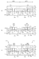
本発明の第1の実施形態に係る半導体装置及びその製造方法について図面を参照しながら説明する。
本発明の第2の実施形態に係る半導体装置及びその製造方法について図面を参照しながら説明する。なお、第2の実施形態に係る半導体装置及びその製造方法について、前述の第1の実施形態に係る半導体装置及びその製造方法と相違する点を中心に説明し、共通する点については適宜省略して説明する。
以下に、本発明の第2の実施形態の変形例に係る半導体装置及びその製造方法について図面を参照しながら説明する。なお、第2の実施形態の変形例に係る半導体装置及びその製造方法について、前述の第2の実施形態に係る半導体装置及びその製造方法と相違する点を中心に説明し、共通する点については適宜省略して説明する。
10a 第1の活性領域
10b 第2の活性領域
11 素子分離領域
12a p型ウェル領域
12b n型ウェル領域
13 ゲート絶縁膜形成膜
13a 第1のゲート絶縁膜
13b 第2のゲート絶縁膜
14,14a,14b 第1の金属膜
15 シリコン膜
15a 第1のシリコン膜
15b 第2のシリコン膜
16 保護膜
16a 第1の保護膜
16b 第2の保護膜
17a 第1のオフセットスペーサ
17b 第2のオフセットスペーサ
18a 浅いn型ソースドレイン領域
18b 浅いp型ソースドレイン領域
19a 第1の内側サイドウォール
19b 第2の内側サイドウォール
20a 第1の外側サイドウォール
20b 第2の外側サイドウォール
20A 第1のサイドウォール
20B 第2のサイドウォール
21,21a 表面保護膜
22 レジストマスク
23 トレンチ
24 シリコン混晶層
25a 深いn型ソースドレイン領域
25b 深いp型ソースドレイン領域
26a 第1の金属シリサイド膜
26b 第2の金属シリサイド膜
27 絶縁膜
28 第1の層間絶縁膜
29 レジストマスク
30,30a,30b 第2の金属膜
30A 第1のゲート電極
30B 第2のゲート電極
31 第2の層間絶縁膜
32a 第1のコンタクトホール
32b 第2のコンタクトホール
33a 第1のコンタクトプラグ
33b 第2のコンタクトプラグ
34 金属シリサイド膜
35 ゲート絶縁膜形成膜
35a 第3のゲート絶縁膜
Wnp 素子分離領域のゲート幅方向の幅
Claims (12)
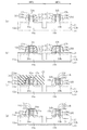
- 第1導電型の第1のMISトランジスタと第2導電型の第2のMISトランジスタとを備えた半導体装置において、
前記第1のMISトランジスタは、
半導体基板における第1の活性領域上に形成された第1のゲート絶縁膜と、
前記第1のゲート絶縁膜上に形成された第2の金属膜からなる第1のゲート電極と、
前記第1のゲート電極の側面上から前記第1の活性領域における前記第1のゲート電極の側方に位置する領域の上面上に跨って形成された絶縁膜とを備え、
前記第2のMISトランジスタは、
前記半導体基板における第2の活性領域上に形成された第2のゲート絶縁膜と、
前記第2のゲート絶縁膜上に形成され第1の金属膜と前記第1の金属膜上に形成された導電膜とからなる第2のゲート電極と、
前記第2のゲート電極の側面上から前記第2の活性領域における前記第2のゲート電極の側方に位置する領域の上面上に跨って形成された前記絶縁膜と、
前記第2の活性領域における前記第2のゲート電極の外側方下に形成された第2導電型のソースドレイン領域とを備え、
前記ソースドレイン領域は、前記第2の活性領域に設けられたトレンチ内に形成され、前記第2の活性領域におけるチャネル領域のゲート長方向に第1の応力を生じさせるシリコン混晶層を含み、
前記第1の金属膜と前記第2の金属膜とは、互いに異なる金属材料からなり、
前記絶縁膜は、前記第1の活性領域におけるチャネル領域のゲート長方向に第2の応力を生じさせる応力絶縁膜であり、
前記第1のゲート電極及び前記第2のゲート電極の各上面上には、前記絶縁膜が形成されていないことを特徴とする半導体装置。 - 請求項1に記載の半導体装置において、
前記第2のMISトランジスタは、p型MISトランジスタであり、
前記シリコン混晶層は、SiGe層からなり、
前記第1の応力は、圧縮応力であることを特徴とする半導体装置。 - 請求項1又は2に記載の半導体装置において、
前記第1の金属膜は、前記第2の金属膜に比べて膜厚が薄いことを特徴とする半導体装置。 - 請求項1〜3のうちいずれか1項に記載の半導体装置において、
前記第1の金属膜と前記第2の金属膜とは、互いに仕事関数が異なっていることを特徴とする半導体装置。 - 請求項1〜4のうちいずれか1項に記載の半導体装置において、
前記絶縁膜の膜厚は、前記第1のゲート電極の膜厚に比べて薄いことを特徴とする半導体装置。 - 請求項1〜5のうちいずれか1項に記載の半導体装置において、
前記導電膜は、前記第2の金属膜からなることを特徴とする半導体装置。 - 請求項1〜5のうちいずれか1項に記載の半導体装置において、
前記導電膜は、シリコン膜からなり、
前記シリコン膜上に形成された金属シリサイド膜をさらに備えていることを特徴とする半導体装置。 - 請求項1〜7のうちいずれか1項に記載の半導体装置において、
前記第1のゲート絶縁膜は、前記第2のゲート絶縁膜と同じ絶縁材料からなることを特徴とする半導体装置。 - 請求項1〜5、7のうちいずれか1項に記載の半導体装置において、
前記第1のゲート絶縁膜は、前記第2のゲート絶縁膜と異なる絶縁材料からなることを特徴とする半導体装置。 - 請求項1〜9のうちいずれか1項に記載の半導体装置において、
前記第1のゲート電極の側面上に形成された断面形状がL字状の第1の内側サイドウォールと、
前記第2のゲート電極の側面上に形成された断面形状がL字状の第2の内側サイドウォールとをさらに備え、
前記絶縁膜は、前記第1の内側サイドウォール及び前記第2の内側サイドウォールの上に接して形成されていることを特徴とする半導体装置。 - 請求項1に記載の半導体装置において、
前記第1のMISトランジスタは、n型MISトランジスタであり、
前記絶縁膜は、シリコン窒化膜からなり、
前記第2の応力は、引っ張り応力であることを特徴とする半導体装置。 - 請求項1〜11のうちいずれか1項に記載の半導体装置において、
前記第1のゲート絶縁膜及び前記第2のゲート絶縁膜は、比誘電率が10以上の金属酸化物からなる高誘電率膜を含むことを特徴とする半導体装置。
Priority Applications (3)
| Application Number | Priority Date | Filing Date | Title |
|---|---|---|---|
| JP2008064435A JP5147471B2 (ja) | 2008-03-13 | 2008-03-13 | 半導体装置 |
| PCT/JP2009/000574 WO2009113241A1 (ja) | 2008-03-13 | 2009-02-13 | 半導体装置及びその製造方法 |
| US12/629,508 US8198686B2 (en) | 2008-03-13 | 2009-12-02 | Semiconductor device |
Applications Claiming Priority (1)
| Application Number | Priority Date | Filing Date | Title |
|---|---|---|---|
| JP2008064435A JP5147471B2 (ja) | 2008-03-13 | 2008-03-13 | 半導体装置 |
Publications (3)
| Publication Number | Publication Date |
|---|---|
| JP2009224386A JP2009224386A (ja) | 2009-10-01 |
| JP2009224386A5 JP2009224386A5 (ja) | 2010-04-08 |
| JP5147471B2 true JP5147471B2 (ja) | 2013-02-20 |
Family
ID=41064914
Family Applications (1)
| Application Number | Title | Priority Date | Filing Date |
|---|---|---|---|
| JP2008064435A Active JP5147471B2 (ja) | 2008-03-13 | 2008-03-13 | 半導体装置 |
Country Status (3)
| Country | Link |
|---|---|
| US (1) | US8198686B2 (ja) |
| JP (1) | JP5147471B2 (ja) |
| WO (1) | WO2009113241A1 (ja) |
Families Citing this family (15)
| Publication number | Priority date | Publication date | Assignee | Title |
|---|---|---|---|---|
| JP5349903B2 (ja) * | 2008-02-28 | 2013-11-20 | ルネサスエレクトロニクス株式会社 | 半導体装置の製造方法および半導体装置 |
| JP5287539B2 (ja) * | 2009-06-23 | 2013-09-11 | 富士通セミコンダクター株式会社 | 半導体装置の製造方法 |
| DE102009055435B4 (de) | 2009-12-31 | 2017-11-09 | Globalfoundries Dresden Module One Limited Liability Company & Co. Kg | Verstärkter Einschluss von Metallgateelektrodenstrukturen mit großem ε durch Verringern der Materialerosion einer dielektrischen Deckschicht beim Erzeugen einer verformungsinduzierenden Halbleiterlegierung |
| DE102010001406B4 (de) * | 2010-01-29 | 2014-12-11 | GLOBALFOUNDRIES Dresden Module One Ltd. Liability Company & Co. KG | Austausch-Gate-Verfahren auf der Grundlage eines früh aufgebrachten Austrittsarbeitsmetalls |
| JP5503735B2 (ja) * | 2010-03-30 | 2014-05-28 | ルネサスエレクトロニクス株式会社 | 半導体装置およびその製造方法 |
| KR101815527B1 (ko) * | 2010-10-07 | 2018-01-05 | 삼성전자주식회사 | 반도체 소자 및 그 제조 방법 |
| JP2012099517A (ja) | 2010-10-29 | 2012-05-24 | Sony Corp | 半導体装置及び半導体装置の製造方法 |
| DE102011003385B4 (de) | 2011-01-31 | 2015-12-03 | Globalfoundries Dresden Module One Limited Liability Company & Co. Kg | Verfahren zur Herstellung einer Halbleiterstruktur mit verformungsinduzierendem Halbleitermaterial |
| US8421132B2 (en) * | 2011-05-09 | 2013-04-16 | International Business Machines Corporation | Post-planarization UV curing of stress inducing layers in replacement gate transistor fabrication |
| US9018090B2 (en) * | 2011-10-10 | 2015-04-28 | International Business Machines Corporation | Borderless self-aligned metal contact patterning using printable dielectric materials |
| US9196708B2 (en) | 2013-12-30 | 2015-11-24 | Taiwan Semiconductor Manufacturing Co., Ltd | Method for forming a semiconductor device structure |
| US9620384B2 (en) * | 2014-07-03 | 2017-04-11 | Globalfoundries Inc. | Control of O-ingress into gate stack dielectric layer using oxygen permeable layer |
| US9589806B1 (en) * | 2015-10-19 | 2017-03-07 | Globalfoundries Inc. | Integrated circuit with replacement gate stacks and method of forming same |
| FR3050315B1 (fr) * | 2016-04-19 | 2019-06-21 | Commissariat A L'energie Atomique Et Aux Energies Alternatives | Transistor a overlap des regions d'acces maitrise |
| FR3069370B1 (fr) * | 2017-07-21 | 2021-10-22 | St Microelectronics Rousset | Circuit integre contenant une structure de leurre |
Family Cites Families (16)
| Publication number | Priority date | Publication date | Assignee | Title |
|---|---|---|---|---|
| US6184083B1 (en) | 1997-06-30 | 2001-02-06 | Kabushiki Kaisha Toshiba | Semiconductor device and method of manufacturing the same |
| JPH1174368A (ja) * | 1997-06-30 | 1999-03-16 | Toshiba Corp | 半導体装置および半導体装置の製造方法 |
| US6261887B1 (en) * | 1997-08-28 | 2001-07-17 | Texas Instruments Incorporated | Transistors with independently formed gate structures and method |
| JP2002118175A (ja) * | 2000-10-05 | 2002-04-19 | Toshiba Corp | 半導体装置及びその製造方法 |
| US6420279B1 (en) * | 2001-06-28 | 2002-07-16 | Sharp Laboratories Of America, Inc. | Methods of using atomic layer deposition to deposit a high dielectric constant material on a substrate |
| JP4011024B2 (ja) | 2004-01-30 | 2007-11-21 | 株式会社ルネサステクノロジ | 半導体装置およびその製造方法 |
| JP4375619B2 (ja) * | 2004-05-26 | 2009-12-02 | 富士通マイクロエレクトロニクス株式会社 | 半導体装置の製造方法 |
| WO2006049834A1 (en) * | 2004-10-29 | 2006-05-11 | Advanced Micro Devices, Inc. | A semiconductor device including semiconductor regions having differently strained channel regions and a method of manufacturing the same |
| DE102004052617B4 (de) | 2004-10-29 | 2010-08-05 | Advanced Micro Devices, Inc., Sunnyvale | Verfahren zur Herstellung eines Halbleiterbauelements und Halbleiterbauelement mit Halbleitergebieten, die unterschiedlich verformte Kanalgebiete aufweisen |
| JP4369379B2 (ja) * | 2005-02-18 | 2009-11-18 | 富士通マイクロエレクトロニクス株式会社 | 半導体装置 |
| JP4723975B2 (ja) | 2005-10-25 | 2011-07-13 | 株式会社東芝 | 半導体装置およびその製造方法 |
| JP2007201063A (ja) | 2006-01-25 | 2007-08-09 | Matsushita Electric Ind Co Ltd | 半導体装置及びその製造方法 |
| JP5055779B2 (ja) * | 2006-02-09 | 2012-10-24 | ソニー株式会社 | 半導体装置の製造方法 |
| JP2007258267A (ja) * | 2006-03-20 | 2007-10-04 | Toshiba Corp | 半導体装置及びその製造方法 |
| JP2007288096A (ja) * | 2006-04-20 | 2007-11-01 | Matsushita Electric Ind Co Ltd | 半導体装置及びその製造方法 |
| US7812414B2 (en) * | 2007-01-23 | 2010-10-12 | Taiwan Semiconductor Manufacturing Company, Ltd. | Hybrid process for forming metal gates |
-
2008
- 2008-03-13 JP JP2008064435A patent/JP5147471B2/ja active Active
-
2009
- 2009-02-13 WO PCT/JP2009/000574 patent/WO2009113241A1/ja active Application Filing
- 2009-12-02 US US12/629,508 patent/US8198686B2/en active Active
Also Published As
| Publication number | Publication date |
|---|---|
| US8198686B2 (en) | 2012-06-12 |
| US20100072523A1 (en) | 2010-03-25 |
| WO2009113241A1 (ja) | 2009-09-17 |
| JP2009224386A (ja) | 2009-10-01 |
Similar Documents
| Publication | Publication Date | Title |
|---|---|---|
| JP5147471B2 (ja) | 半導体装置 | |
| US11018241B2 (en) | Polysilicon design for replacement gate technology | |
| US11121133B2 (en) | Semiconductor device with fin transistors and manufacturing method of such semiconductor device | |
| US20130260549A1 (en) | Replacement gate with reduced gate leakage current | |
| US8871585B2 (en) | Manufacturing method of semiconductor device and semiconductor device | |
| KR20100003241A (ko) | 반도체 장치 및 반도체 장치의 제조 방법 | |
| US8237205B2 (en) | Semiconductor device and method for fabricating the same | |
| JP2007251030A (ja) | 半導体装置の製造方法および半導体装置 | |
| JP2008288465A (ja) | 半導体装置及びその製造方法 | |
| JP2008140853A (ja) | 半導体装置及びその製造方法 | |
| WO2011021316A1 (ja) | 半導体装置及びその製造方法 | |
| TWI690984B (zh) | 半導體元件及其製作方法 | |
| JP3998665B2 (ja) | 半導体装置およびその製造方法 | |
| US7755145B2 (en) | Semiconductor device and manufacturing method thereof | |
| US8471341B2 (en) | Semiconductor device and method for fabricating the same | |
| JP2009117621A (ja) | 半導体装置及びその製造方法 | |
| JP2006013270A (ja) | 半導体装置およびその製造方法 | |
| JP2007287793A (ja) | 半導体装置の製造方法 | |
| JP2008187150A (ja) | 半導体装置及びその製造方法 | |
| WO2012077256A1 (ja) | 半導体装置及びその製造方法 | |
| TW202105618A (zh) | 半導體裝置及其製造方法 | |
| WO2010116587A1 (ja) | 半導体装置及びその製造方法 |
Legal Events
| Date | Code | Title | Description |
|---|---|---|---|
| A521 | Request for written amendment filed |
Free format text: JAPANESE INTERMEDIATE CODE: A523 Effective date: 20100223 |
|
| A621 | Written request for application examination |
Free format text: JAPANESE INTERMEDIATE CODE: A621 Effective date: 20100223 |
|
| RD02 | Notification of acceptance of power of attorney |
Free format text: JAPANESE INTERMEDIATE CODE: A7422 Effective date: 20120130 |
|
| A131 | Notification of reasons for refusal |
Free format text: JAPANESE INTERMEDIATE CODE: A131 Effective date: 20120807 |
|
| A521 | Request for written amendment filed |
Free format text: JAPANESE INTERMEDIATE CODE: A523 Effective date: 20120911 |
|
| TRDD | Decision of grant or rejection written | ||
| A01 | Written decision to grant a patent or to grant a registration (utility model) |
Free format text: JAPANESE INTERMEDIATE CODE: A01 Effective date: 20121113 |
|
| A61 | First payment of annual fees (during grant procedure) |
Free format text: JAPANESE INTERMEDIATE CODE: A61 Effective date: 20121127 |
|
| R150 | Certificate of patent or registration of utility model |
Ref document number: 5147471 Country of ref document: JP Free format text: JAPANESE INTERMEDIATE CODE: R150 Free format text: JAPANESE INTERMEDIATE CODE: R150 |
|
| FPAY | Renewal fee payment (event date is renewal date of database) |
Free format text: PAYMENT UNTIL: 20151207 Year of fee payment: 3 |
|
| S111 | Request for change of ownership or part of ownership |
Free format text: JAPANESE INTERMEDIATE CODE: R313113 |
|
| R350 | Written notification of registration of transfer |
Free format text: JAPANESE INTERMEDIATE CODE: R350 |
|
| R250 | Receipt of annual fees |
Free format text: JAPANESE INTERMEDIATE CODE: R250 |
|
| R250 | Receipt of annual fees |
Free format text: JAPANESE INTERMEDIATE CODE: R250 |
|
| R250 | Receipt of annual fees |
Free format text: JAPANESE INTERMEDIATE CODE: R250 |
|
| R250 | Receipt of annual fees |
Free format text: JAPANESE INTERMEDIATE CODE: R250 |