WO2009084244A1 - 露光装置、移動体駆動システム、パターン形成装置、及び露光方法、並びにデバイス製造方法 - Google Patents
露光装置、移動体駆動システム、パターン形成装置、及び露光方法、並びにデバイス製造方法 Download PDFInfo
- Publication number
- WO2009084244A1 WO2009084244A1 PCT/JP2008/004044 JP2008004044W WO2009084244A1 WO 2009084244 A1 WO2009084244 A1 WO 2009084244A1 JP 2008004044 W JP2008004044 W JP 2008004044W WO 2009084244 A1 WO2009084244 A1 WO 2009084244A1
- Authority
- WO
- WIPO (PCT)
- Prior art keywords
- exposure
- moving body
- measurement
- axis
- wafer
- Prior art date
Links
Images


Classifications
-
- G—PHYSICS
- G03—PHOTOGRAPHY; CINEMATOGRAPHY; ANALOGOUS TECHNIQUES USING WAVES OTHER THAN OPTICAL WAVES; ELECTROGRAPHY; HOLOGRAPHY
- G03F—PHOTOMECHANICAL PRODUCTION OF TEXTURED OR PATTERNED SURFACES, e.g. FOR PRINTING, FOR PROCESSING OF SEMICONDUCTOR DEVICES; MATERIALS THEREFOR; ORIGINALS THEREFOR; APPARATUS SPECIALLY ADAPTED THEREFOR
- G03F7/00—Photomechanical, e.g. photolithographic, production of textured or patterned surfaces, e.g. printing surfaces; Materials therefor, e.g. comprising photoresists; Apparatus specially adapted therefor
- G03F7/70—Microphotolithographic exposure; Apparatus therefor
- G03F7/70216—Mask projection systems
- G03F7/70341—Details of immersion lithography aspects, e.g. exposure media or control of immersion liquid supply
-
- G—PHYSICS
- G03—PHOTOGRAPHY; CINEMATOGRAPHY; ANALOGOUS TECHNIQUES USING WAVES OTHER THAN OPTICAL WAVES; ELECTROGRAPHY; HOLOGRAPHY
- G03F—PHOTOMECHANICAL PRODUCTION OF TEXTURED OR PATTERNED SURFACES, e.g. FOR PRINTING, FOR PROCESSING OF SEMICONDUCTOR DEVICES; MATERIALS THEREFOR; ORIGINALS THEREFOR; APPARATUS SPECIALLY ADAPTED THEREFOR
- G03F7/00—Photomechanical, e.g. photolithographic, production of textured or patterned surfaces, e.g. printing surfaces; Materials therefor, e.g. comprising photoresists; Apparatus specially adapted therefor
- G03F7/70—Microphotolithographic exposure; Apparatus therefor
- G03F7/70425—Imaging strategies, e.g. for increasing throughput or resolution, printing product fields larger than the image field or compensating lithography- or non-lithography errors, e.g. proximity correction, mix-and-match, stitching or double patterning
-
- G—PHYSICS
- G03—PHOTOGRAPHY; CINEMATOGRAPHY; ANALOGOUS TECHNIQUES USING WAVES OTHER THAN OPTICAL WAVES; ELECTROGRAPHY; HOLOGRAPHY
- G03F—PHOTOMECHANICAL PRODUCTION OF TEXTURED OR PATTERNED SURFACES, e.g. FOR PRINTING, FOR PROCESSING OF SEMICONDUCTOR DEVICES; MATERIALS THEREFOR; ORIGINALS THEREFOR; APPARATUS SPECIALLY ADAPTED THEREFOR
- G03F7/00—Photomechanical, e.g. photolithographic, production of textured or patterned surfaces, e.g. printing surfaces; Materials therefor, e.g. comprising photoresists; Apparatus specially adapted therefor
- G03F7/70—Microphotolithographic exposure; Apparatus therefor
- G03F7/70483—Information management; Active and passive control; Testing; Wafer monitoring, e.g. pattern monitoring
- G03F7/7055—Exposure light control in all parts of the microlithographic apparatus, e.g. pulse length control or light interruption
-
- G—PHYSICS
- G03—PHOTOGRAPHY; CINEMATOGRAPHY; ANALOGOUS TECHNIQUES USING WAVES OTHER THAN OPTICAL WAVES; ELECTROGRAPHY; HOLOGRAPHY
- G03F—PHOTOMECHANICAL PRODUCTION OF TEXTURED OR PATTERNED SURFACES, e.g. FOR PRINTING, FOR PROCESSING OF SEMICONDUCTOR DEVICES; MATERIALS THEREFOR; ORIGINALS THEREFOR; APPARATUS SPECIALLY ADAPTED THEREFOR
- G03F7/00—Photomechanical, e.g. photolithographic, production of textured or patterned surfaces, e.g. printing surfaces; Materials therefor, e.g. comprising photoresists; Apparatus specially adapted therefor
- G03F7/70—Microphotolithographic exposure; Apparatus therefor
- G03F7/70691—Handling of masks or workpieces
- G03F7/70775—Position control, e.g. interferometers or encoders for determining the stage position
-
- G—PHYSICS
- G03—PHOTOGRAPHY; CINEMATOGRAPHY; ANALOGOUS TECHNIQUES USING WAVES OTHER THAN OPTICAL WAVES; ELECTROGRAPHY; HOLOGRAPHY
- G03F—PHOTOMECHANICAL PRODUCTION OF TEXTURED OR PATTERNED SURFACES, e.g. FOR PRINTING, FOR PROCESSING OF SEMICONDUCTOR DEVICES; MATERIALS THEREFOR; ORIGINALS THEREFOR; APPARATUS SPECIALLY ADAPTED THEREFOR
- G03F7/00—Photomechanical, e.g. photolithographic, production of textured or patterned surfaces, e.g. printing surfaces; Materials therefor, e.g. comprising photoresists; Apparatus specially adapted therefor
- G03F7/70—Microphotolithographic exposure; Apparatus therefor
- G03F7/708—Construction of apparatus, e.g. environment aspects, hygiene aspects or materials
- G03F7/70908—Hygiene, e.g. preventing apparatus pollution, mitigating effect of pollution or removing pollutants from apparatus
-
- G—PHYSICS
- G03—PHOTOGRAPHY; CINEMATOGRAPHY; ANALOGOUS TECHNIQUES USING WAVES OTHER THAN OPTICAL WAVES; ELECTROGRAPHY; HOLOGRAPHY
- G03F—PHOTOMECHANICAL PRODUCTION OF TEXTURED OR PATTERNED SURFACES, e.g. FOR PRINTING, FOR PROCESSING OF SEMICONDUCTOR DEVICES; MATERIALS THEREFOR; ORIGINALS THEREFOR; APPARATUS SPECIALLY ADAPTED THEREFOR
- G03F7/00—Photomechanical, e.g. photolithographic, production of textured or patterned surfaces, e.g. printing surfaces; Materials therefor, e.g. comprising photoresists; Apparatus specially adapted therefor
- G03F7/70—Microphotolithographic exposure; Apparatus therefor
- G03F7/708—Construction of apparatus, e.g. environment aspects, hygiene aspects or materials
- G03F7/70975—Assembly, maintenance, transport or storage of apparatus
-
- G—PHYSICS
- G03—PHOTOGRAPHY; CINEMATOGRAPHY; ANALOGOUS TECHNIQUES USING WAVES OTHER THAN OPTICAL WAVES; ELECTROGRAPHY; HOLOGRAPHY
- G03F—PHOTOMECHANICAL PRODUCTION OF TEXTURED OR PATTERNED SURFACES, e.g. FOR PRINTING, FOR PROCESSING OF SEMICONDUCTOR DEVICES; MATERIALS THEREFOR; ORIGINALS THEREFOR; APPARATUS SPECIALLY ADAPTED THEREFOR
- G03F9/00—Registration or positioning of originals, masks, frames, photographic sheets or textured or patterned surfaces, e.g. automatically
- G03F9/70—Registration or positioning of originals, masks, frames, photographic sheets or textured or patterned surfaces, e.g. automatically for microlithography
- G03F9/7073—Alignment marks and their environment
-
- G—PHYSICS
- G03—PHOTOGRAPHY; CINEMATOGRAPHY; ANALOGOUS TECHNIQUES USING WAVES OTHER THAN OPTICAL WAVES; ELECTROGRAPHY; HOLOGRAPHY
- G03F—PHOTOMECHANICAL PRODUCTION OF TEXTURED OR PATTERNED SURFACES, e.g. FOR PRINTING, FOR PROCESSING OF SEMICONDUCTOR DEVICES; MATERIALS THEREFOR; ORIGINALS THEREFOR; APPARATUS SPECIALLY ADAPTED THEREFOR
- G03F9/00—Registration or positioning of originals, masks, frames, photographic sheets or textured or patterned surfaces, e.g. automatically
- G03F9/70—Registration or positioning of originals, masks, frames, photographic sheets or textured or patterned surfaces, e.g. automatically for microlithography
- G03F9/7088—Alignment mark detection, e.g. TTR, TTL, off-axis detection, array detector, video detection
-
- G—PHYSICS
- G03—PHOTOGRAPHY; CINEMATOGRAPHY; ANALOGOUS TECHNIQUES USING WAVES OTHER THAN OPTICAL WAVES; ELECTROGRAPHY; HOLOGRAPHY
- G03F—PHOTOMECHANICAL PRODUCTION OF TEXTURED OR PATTERNED SURFACES, e.g. FOR PRINTING, FOR PROCESSING OF SEMICONDUCTOR DEVICES; MATERIALS THEREFOR; ORIGINALS THEREFOR; APPARATUS SPECIALLY ADAPTED THEREFOR
- G03F9/00—Registration or positioning of originals, masks, frames, photographic sheets or textured or patterned surfaces, e.g. automatically
- G03F9/70—Registration or positioning of originals, masks, frames, photographic sheets or textured or patterned surfaces, e.g. automatically for microlithography
- G03F9/7096—Arrangement, mounting, housing, environment, cleaning or maintenance of apparatus
-
- Y—GENERAL TAGGING OF NEW TECHNOLOGICAL DEVELOPMENTS; GENERAL TAGGING OF CROSS-SECTIONAL TECHNOLOGIES SPANNING OVER SEVERAL SECTIONS OF THE IPC; TECHNICAL SUBJECTS COVERED BY FORMER USPC CROSS-REFERENCE ART COLLECTIONS [XRACs] AND DIGESTS
- Y10—TECHNICAL SUBJECTS COVERED BY FORMER USPC
- Y10T—TECHNICAL SUBJECTS COVERED BY FORMER US CLASSIFICATION
- Y10T29/00—Metal working
- Y10T29/49—Method of mechanical manufacture
- Y10T29/49002—Electrical device making
Definitions
- the present invention relates to an exposure apparatus, a moving body drive system, a pattern forming apparatus, an exposure method, and a device manufacturing method, and more particularly, used in a lithography process when manufacturing an electronic device such as a semiconductor element or a liquid crystal display element.
- steppers step-and-repeat type projection exposure apparatuses
- steppers step-and-scan type Projection exposure apparatuses
- scanning steppers also called scanners
- peripheral exposure is performed in which a portion that cannot be used as a device is exposed in a shot region (hereinafter referred to as “peripheral shot”) that partially protrudes from the effective exposure region in the peripheral portion of the wafer.
- peripheral shot a shot region that partially protrudes from the effective exposure region in the peripheral portion of the wafer.
- the throughput is reduced by the time required for the peripheral exposure.
- a twin wafer stage type exposure that employs a technique in which a plurality of, for example, two wafer stages for holding wafers are provided and different operations are processed in parallel on the two wafer stages.
- Various devices have been proposed.
- an exposure apparatus of a twin wafer stage type employing an immersion exposure method has been proposed (see, for example, Patent Document 2).
- the device rule (practical minimum line width) is gradually miniaturized, and accordingly, the exposure apparatus is required to have a higher precision overlay performance. For this reason, the number of sample shots of enhanced global alignment (EGA), which is the mainstream of wafer alignment, is expected to increase further, and even with a twin wafer stage type exposure apparatus, there is a concern about a decrease in throughput.
- EGA enhanced global alignment
- the position of a stage holding a wafer is generally measured using a laser interferometer.
- the required performance has become severe due to the miniaturization of patterns due to the high integration of semiconductor elements, and now the air fluctuations caused by the temperature change and / or temperature gradient of the laser interferometer beam path. Short-term fluctuations in measured values due to inequality are no longer negligible.
- an exposure apparatus that exposes an object with an exposure beam, and moves along a predetermined plane including a first axis and a second axis that are orthogonal to each other while holding the object.
- a measurement system that is arranged in a direction parallel to the first axis from an exposure position where the exposure is performed, and performs predetermined measurement on the object; and from the measurement system in a direction parallel to the first axis
- a first exposure apparatus comprising: a peripheral exposure system that is disposed separately and exposes at least a part of a shot area around the object.
- the peripheral exposure system at least a part of the shot area around the object is exposed by the peripheral exposure system while the moving body that holds the object moves along the direction parallel to the first axis in the predetermined plane. Accordingly, the movement of the object (moving body) from the measurement system toward the exposure position or the movement of the object (moving body) in the opposite direction (for example, movement of the moving body from the exposure position to the object replacement position) is performed in parallel.
- the peripheral exposure can be performed, and unlike the case where the peripheral exposure is performed independently, the throughput is hardly lowered.
- an exposure apparatus for exposing an object with an exposure beam, wherein the object is held in the predetermined plane including a first axis and a second axis that are orthogonal to each other.
- a peripheral exposure system that exposes at least a part of a peripheral region different from the region to be displayed, and in parallel with the movement of the movable body from one of the exposure position and the replacement position to the other, It is a 2nd exposure apparatus with which at least one part of exposure operation is performed.
- the present invention is an exposure apparatus that exposes an object with an energy beam to form a pattern on the object, and includes a first axis and a second axis that hold the object and are orthogonal to each other.
- a first moving body that moves in a predetermined plane; a second moving body that holds an object and moves independently of the first moving body in the plane; and a position in a direction parallel to the second axis
- a mark detection system having a plurality of different detection areas and detecting a mark on the object placed on each of the first and second moving bodies; and held by one of the first and second moving bodies In parallel with the exposure of the object, the other one of the first and second moving bodies is moved in a direction parallel to the first axis, and the object held by the other moving body is different.
- a plurality of marks are detected by the mark detection system and the position information is obtained.
- a third exposure apparatus provided with; controller and for measuring.
- the other of the first and second moving bodies is parallel to the first axis. While moving in the direction, a plurality of different marks on the object held by the other moving body are detected by the mark detection system, and the position information is measured. Accordingly, in parallel with the exposure of the object held on one moving body, the other moving body is positioned in the vicinity of a plurality of detection areas of the mark detection system (for example, replacement of the object held on the moving body).
- the present invention is an exposure apparatus that exposes an object with an energy beam to form a pattern on the object, and includes a first axis and a second axis that hold the object and are orthogonal to each other.
- a first moving body that moves in a predetermined plane; a second moving body that holds an object and moves independently of the first moving body in the plane; and the first and second moving bodies are A planar motor that drives in a plane; and controls the planar motor, and when the exposure of the object held by the first movable body is completed, the first movable body is exposed at the exposure position where the exposure is performed.
- a control device that moves the object on the second moving body to a second exchange position where the object is exchanged along a second feedback path located on the other side in a direction parallel to the second axis. It is an exposure apparatus.
- first exchange position and the second exchange position may be the same or different.
- the control device controls the planar motor that drives the first and second moving bodies in the plane, and the first time when the exposure of the object held by the first moving body is completed.
- the moving body is moved to the first exchange position where the object on the first moving body is exchanged along the first feedback path located on one side of the exposure position in the direction parallel to the second axis, and the second movement
- the second moving body moves along the second feedback path in which the second moving body is located on the other side in the direction parallel to the second axis of the exposure position. It moves to the 2nd exchange position where exchange is performed.
- the cable for wiring and piping is attached to the first moving body from one side in the direction parallel to the second axis, and the second moving body is attached from the other side in the direction parallel to the second axis.
- the cables can be prevented from being twisted and the length thereof can be shortened as much as possible.
- the present invention is an exposure apparatus that exposes an object with an energy beam to form a pattern on the object, and includes a first axis and a second axis that hold the object and are orthogonal to each other.
- a first moving body that moves in a predetermined plane; a second moving body that holds an object and moves independently of the first moving body in the plane; and the first and second moving bodies are moved to the plane.
- a liquid immersion device that forms a liquid immersion region by supplying a liquid between the optical member and one of the first and second moving bodies. And after the exposure of the object held by the one moving body is completed, the first moving body and the second moving body are transferred to pass the immersion area from the one moving body to the other moving body.
- the moving body is switched to a separated state in which the moving body is separated, and the one moving body separated from the other moving body is moved to a return path located on one side of the exposure position with respect to a direction parallel to the second axis.
- a control device that controls the planar motor so as to move the object on the first and second moving bodies to an exchange position where the object is exchanged.
- the proximity state in which the first moving body and the second moving body are brought closer to each other below a predetermined distance, the first moving body and the second moving body are brought into contact with each other in the direction parallel to the first axis, that is, the first moving body and the second moving body are separated.
- the term “proximity state” is used as a concept including the state where the separation distance is zero, that is, the contact state even when there is an explicit state of contact, and even when there is no explicit state.
- the liquid immersion area is passed from one moving body to the other moving body, so that both moving bodies are parallel to the first axis.
- Switching between a proximity state in which the direction is close to a predetermined distance or less and a separation state in which both moving bodies are separated is performed, and one moving body that is separated from the other moving body is switched in a direction parallel to the second axis.
- the planar motor is controlled to move to an exchange position where the objects on the first and second moving bodies are exchanged along a return path located on one side of the exposure position.
- one moving body is moved to the replacement position along a feedback path located on one side of the exposure position with respect to the direction parallel to the second axis, and the other moving body is exposed to the position parallel to the second axis.
- the moving range in the direction parallel to the second axis of both moving bodies can be set narrower.
- the present invention is a moving body drive system for driving a moving body substantially along a predetermined plane, and first and second directions orthogonal to each other in a plane parallel to the predetermined plane. Irradiating detection light to a scale having a two-dimensional grating having a periodic direction as a periodic direction, and receiving a light from the scale, and including the first and second directions based on a measurement value of the head
- An encoder system for measuring positional information of the moving body in at least two directions of freedom within a predetermined plane; and a driving device for driving the moving body along the predetermined plane based on the measurement information of the encoder system;
- a movable body drive system is provided.
- the predetermined plane including the first and second directions based on the measurement value of the head, having a head that irradiates the scale having the two-dimensional grating with the detection light and receives the reflected light from the scale.
- the driving apparatus drives the moving body along a predetermined plane. Therefore, the degree of freedom in the arrangement of the heads is greatly improved and the layout is facilitated as compared with the case where an encoder system including a plurality of one-dimensional heads that respectively measure the position information of the moving body in the first and second directions is used. For example, by using only one scale, it is possible to measure the position of the moving body in the direction of two degrees of freedom in a plane parallel to the predetermined plane.
- the present invention provides a moving body on which an object is placed and which can move substantially along a moving surface while holding the object; and a patterning device that generates a pattern on the object; And a moving body driving system of the present invention for driving the moving body to form a pattern on the object.
- an exposure apparatus for forming a pattern on an object by irradiation with an energy beam, the patterning apparatus for irradiating the object with the energy beam; and the moving body drive system of the present invention; And a sixth exposure apparatus that drives the movable body on which the object is placed by the movable body drive system for relative movement between the energy beam and the object.
- the moving body on which the object is placed is driven with high accuracy by the moving body drive system of the present invention for the relative movement between the energy beam irradiated to the object from the patterning device and the object. Accordingly, it is possible to form a pattern on the object with high accuracy by scanning exposure.
- an exposure apparatus for exposing an object with an energy beam, a movable body capable of holding the object and substantially movable along a predetermined plane;
- a measuring device for measuring the position information of the object, the measuring position being irradiated with the measuring beam apart from the exposure position irradiated with the energy beam with respect to one direction; and orthogonal to the first direction within the predetermined plane;
- Scales having the first direction as a longitudinal direction and having a two-dimensional lattice are disposed on both sides of the moving body with respect to the second direction, and at least one head can face each of the two scales.
- a pair of head units having a plurality of heads with different positions with respect to the direction are arranged so as to be able to face the moving body, and face simultaneously with the pair of scales
- An encoder system that measures position information of the moving body in the direction of three degrees of freedom within the predetermined plane based on outputs of two heads; position information of the object measured by the measuring device; and measurement by the encoder system
- a driving device that drives the moving body based on the positional information of the moving body that has been made.
- the position information of the object on the moving body is measured by the measurement device at the measurement position irradiated with the measurement beam, which is arranged away from the exposure position in the first direction within the predetermined plane, and the encoder system
- the position information of the moving body in the direction of three degrees of freedom within the predetermined plane is measured, and measured by the driving device with the measuring device
- the moving body is driven with high accuracy based on the position information of the object and the position information of the moving body measured by the encoder system. Therefore, it becomes possible to expose the object held by the moving body with high accuracy.
- the layout of the heads and the like is facilitated as compared with the case of using an encoder system including a plurality of one-dimensional heads that respectively measure the position information of the moving body in the first and second directions.
- an exposure apparatus that exposes an object with an energy beam, a movable body capable of holding the object and substantially movable along a predetermined plane;
- a measuring device for measuring the position information of the object, the measuring position being irradiated with the measuring beam apart from the exposure position irradiated with the energy beam with respect to one direction; and orthogonal to the first direction within the predetermined plane;
- a pair of scales having a second direction as a longitudinal direction and having a two-dimensional lattice are disposed so as to be able to face the moving body, and at least one head can be opposed to the pair of scales and be positioned with respect to the first direction.
- a plurality of heads having different heads are arranged on both sides of the moving body, and the predetermined heads are based on outputs of two heads facing each other simultaneously with the pair of scales.
- the position information of the object on the moving body is measured by the measurement device at the measurement position irradiated with the measurement beam, which is arranged away from the exposure position in the first direction within the predetermined plane, and the encoder system Based on the outputs of the two heads facing each other simultaneously with the pair of scales, the position information of the moving body in the three-degree-of-freedom direction in the predetermined plane is measured, and the driving device measures the object measured by the measuring device.
- the moving body is driven with high accuracy based on the position information and the position information of the moving body measured by the encoder system. Therefore, it becomes possible to expose the object held by the moving body with high accuracy.
- the arrangement of the head on the moving body is facilitated as compared to the case of using an encoder system including a plurality of one-dimensional heads that respectively measure the position information of the moving body in the first and second directions.
- a first device including exposing an object using any of the first to eighth exposure apparatuses of the present invention and developing the exposed object. It is a manufacturing method.
- an exposure method for exposing an object with an exposure beam wherein the object is placed on a moving body that moves along a predetermined plane including a first axis and a second axis orthogonal to each other.
- a first axis of a measurement system that is disposed away from an exposure position where the exposure is performed in a direction parallel to the first axis in the predetermined plane and performs predetermined measurement on the object.
- the peripheral exposure system at least a part of the shot area around the object is exposed by the peripheral exposure system while the moving body on which the object is placed moves along the direction parallel to the first axis in the predetermined plane. Is done. Accordingly, the movement of the object (moving body) from the measurement system toward the exposure position or the movement of the object (moving body) in the opposite direction (for example, movement of the moving body from the exposure position to the object replacement position) is performed in parallel.
- the peripheral exposure can be performed, and unlike the case where the peripheral exposure is performed independently, the throughput is hardly lowered.
- an exposure method for exposing an object with an exposure beam wherein the object is held by a movable body movable within a predetermined plane including a first axis and a second axis orthogonal to each other. And an exposure position at which the exposure is performed and an exchange position of the object arranged away from the exposure position in a direction parallel to the first axis, and the exposure is performed on the object.
- the peripheral exposure system that exposes at least a part of the peripheral region different from the region to be exposed, exposing the peripheral region in parallel with the movement of the moving body from one of the exposure position and the replacement position to the other. And a step of performing at least a part of the operation.
- an exposure method for exposing an object with an energy beam to form a pattern on the object wherein the first axis and the second axis orthogonal to each other are respectively held by holding the object.
- a mark detection system having a plurality of detection regions having different positions with respect to a direction parallel to the second axis while moving a plurality of different marks on the object held by the other moving body while moving in a direction parallel to the axis
- It is the 3rd exposure method including the process of detecting and measuring the position information.
- the other of the first and second moving bodies is moved in a direction parallel to the first axis.
- a plurality of different marks on the object held by the other moving body are detected by a mark detection system having a plurality of detection regions having different positions with respect to the direction parallel to the second axis, and the position information is measured.
- the other moving body is positioned in the vicinity of a plurality of detection areas of the mark detection system (for example, the object held by the moving body).
- the position information of a plurality of marks for example, all marks on the object held by the other moving body is detected. It becomes possible to do. As a result, it is possible to improve throughput and improve overlay accuracy.
- an exposure method in which an object is exposed with an energy beam to form a pattern on the object, and the first axis and the second axis orthogonal to each other are respectively held by holding the object.
- the first movement when the exposure of the object held by the first moving body is completed by controlling the plane motors that drive the first and second moving bodies that move independently within a predetermined plane including the first moving body.
- the body is moved to a first exchange position where an object on the first moving body is exchanged along a first feedback path located on one side in a direction parallel to the second axis of the exposure position where the exposure is performed.
- the second moving body When the exposure of the object held by the second moving body is completed, the second moving body is placed on a second feedback path located on the other side of the exposure position in a direction parallel to the second axis.
- a second exchange position where an object on the second moving body is exchanged along
- a fourth exposure method comprising the step of moving to.
- the first moving body is exposed when the exposure of the object held by the first moving body is completed by controlling the planar motor that drives the first and second moving bodies in the plane.
- the position of the object on the first moving body is moved along the first return path located on one side in the direction parallel to the second axis of the position to the first exchanging position where the object is exchanged, and is held by the second moving body.
- the object on the second moving body is exchanged along the second feedback path that is located on the other side of the second moving body in the direction parallel to the second axis of the exposure position. Move to the second exchange position.
- the cable for wiring and piping is attached to the first moving body from one side in the direction parallel to the second axis, and the second moving body is attached from the other side in the direction parallel to the second axis.
- the cables can be prevented from being twisted and the length thereof can be shortened as much as possible.
- an exposure method for exposing an object with an energy beam wherein the object is held by a moving body; and the moving body is driven by the moving body driving system of the present invention. And exposing the object with the energy beam.
- the moving body holding the object is accurately driven by the moving body drive system of the present invention and the object is exposed with the energy beam, the object can be exposed with high accuracy.
- an exposure method for exposing an object with an energy beam wherein the object is held by a movable body substantially movable along a predetermined plane; Measuring positional information of an object on the moving body at a measurement position irradiated with a measurement beam, which is arranged apart from an exposure position irradiated with the energy beam with respect to one direction;
- a pair of scales having the first direction as a longitudinal direction and having a two-dimensional lattice are disposed on the movable body apart from each other in a second direction orthogonal to the first direction, and at least one of each of the pair of scales
- An encoder system in which a pair of head units having a plurality of heads that can be opposed to each other and have different positions with respect to the second direction is arranged to be able to face the moving body, Measuring position information of the moving body in a direction of three degrees of freedom within a predetermined plane; driving the moving body based on the measured position information
- the position information of the object on the moving body is measured at the measurement position irradiated with the measurement beam, which is arranged away from the exposure position in the first direction in the predetermined plane, and the predetermined plane is obtained by the encoder system.
- the position information of the moving body in the three degrees of freedom direction is measured.
- the moving body is driven based on the measured position information and the measurement information of the encoder system, and the object is exposed with the energy beam. Therefore, the object can be exposed with high accuracy.
- an exposure method for exposing an object with an energy beam wherein the object is held by a movable body substantially movable along a predetermined plane; Measuring positional information of an object on the moving body at a measurement position irradiated with a measurement beam, which is arranged apart from an exposure position irradiated with the energy beam with respect to one direction; A pair of scales having a second direction orthogonal to the first direction as a longitudinal direction and having a two-dimensional lattice are disposed so as to be able to face the moving body, and at least one head can face each of the pair of scales, and A plurality of heads having different positions with respect to the first direction are related to a direction of three degrees of freedom within the predetermined plane by an encoder system arranged on each side of the movable body. Measuring position information of the moving body; driving the moving body based on the measured position information and measurement information of the encoder system, and exposing the object with
- the position information of the object on the moving body is measured at the measurement position irradiated with the measurement beam, which is arranged away from the exposure position in the first direction in the predetermined plane, and the predetermined plane is obtained by the encoder system.
- the position information of the moving body in the three degrees of freedom direction is measured.
- the moving body is driven based on the measured position information and the measurement information of the encoder system, and the object is exposed with the energy beam. Therefore, the object can be exposed with high accuracy.
- an object is exposed to form a pattern by any one of the first to seventh exposure methods of the present invention; and the object on which the pattern is formed is developed. And a second device manufacturing method.
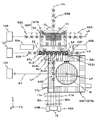
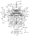
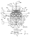
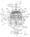
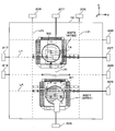
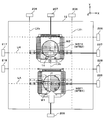
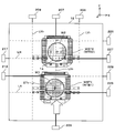
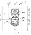
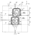
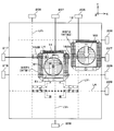
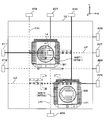
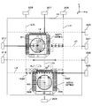
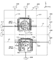
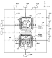
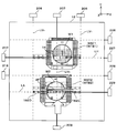
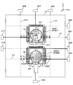
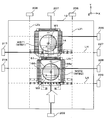
- FIG. 9A and FIG. 9A show schematically the structure of the exposure apparatus which concerns on 1st Embodiment. It is a top view which shows a wafer stage. It is a top view which shows a measurement stage. It is a figure for demonstrating an interferometer system. It is a top view which shows a stage apparatus and various measuring devices. It is a figure for demonstrating arrangement
- FIG. 9B are diagrams for explaining an on state and an off state of the micromirror, respectively.
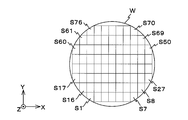
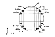
- FIG. 2 is a block diagram showing a main configuration of a control system in the exposure apparatus of FIG. 1. It is a figure for demonstrating the shot map of a wafer. It is a figure for demonstrating the alignment shot area
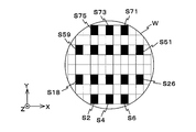
- FIG. 6 is a diagram showing a state of a wafer stage and a measurement stage when alignment marks attached to five second alignment shot areas are simultaneously detected using alignment systems AL1, AL2 1 to AL2 4 . It is a figure which shows the state of a wafer stage and the measurement stage when at least one of the process of Pri-BCHK latter half and the process of focus calibration latter half is performed.
- FIG. 6 is a diagram showing the state of a wafer stage and a measurement stage when alignment marks attached to five third alignment shot areas are simultaneously detected using alignment systems AL1, AL2 1 to AL2 4 .
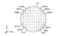
- FIG. 25A to FIG. 25F are diagrams for explaining the process of peripheral exposure. It is a figure which shows all the areas
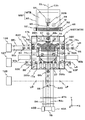
- FIG. 43A is a side view showing wafer stage WST1 in FIG. 42
- FIG. 43B is a plan view showing wafer stage WST1.
- 44A is a side view showing wafer stage WST2 in FIG. 42
- FIG. 44B is a plan view showing wafer stage WST2.
- FIG. 43 is a diagram for explaining an arrangement of heads and the like of an encoder system and a surface position measurement system that constitute a measurement system included in the wafer stage apparatus of FIG. 42.
- FIG. 5 is a diagram (No. 1) for describing a parallel processing operation using wafer stages WST1 and WST2.
- FIG. 10 is a diagram (No. 2) for explaining the parallel processing operation using wafer stage WST1 and WST2.
- FIG. 11 is a diagram (No. 3) for explaining the parallel processing operation using wafer stage WST1 and WST2.
- FIG. 11 is a diagram (No. 4) for explaining the parallel processing operation using wafer stage WST1 and WST2.
- FIG. 11 is a diagram (No.
- FIG. 10 is a view (No. 6) used to explain a parallel processing operation using wafer stage WST1 and WST2;
- FIG. 10 is a view (No. 7) used to explain a parallel processing operation using wafer stage WST1 and WST2;
- FIG. 10 is a view (No. 8) used to explain a parallel processing operation using wafer stage WST1 and WST2;
- FIG. 10 is a view (No. 9) used to explain a parallel processing operation using wafer stage WST1 and WST2;
- FIG. 10 is a view (No. 10) used to explain a parallel processing operation using wafer stage WST1 and WST2;
- FIG. 11 is a view (No.
- FIG. 11 used to explain a parallel processing operation using wafer stage WST1 and WST2
- FIG. 12 is a view (No. 12) used to explain a parallel processing operation using wafer stage WST1 and WST2
- FIG. 19 is a view (No. 13) used to explain a parallel processing operation using wafer stage WST1 and WST2
- FIG. 14 is a view (No. 14) used to explain a parallel processing operation using wafer stage WST1 and WST2
- FIG. 22 is a view (No. 15) used to explain a parallel processing operation using wafer stage WST1 and WST2
- FIG. 16 is a view (No. 16) used to explain a parallel processing operation using wafer stage WST1 and WST2
- FIG. 17 is a view (No.
- FIG. 17 used to explain a parallel processing operation using wafer stage WST1 and WST2;
- FIG. 18 is a view (No. 18) used to explain a parallel processing operation using wafer stage WST1 and WST2;
- FIG. 20 is a view (No. 19) used to explain a parallel processing operation using wafer stage WST1 and WST2;
- FIG. 20 is a view (No. 20) used to explain a parallel processing operation using wafer stage WST1 and WST2;
- FIG. 22 is a view (No. 21) used to explain a parallel processing operation using wafer stage WST1 and WST2;
- FIG. 22 is a view (No. 22) used to explain a parallel processing operation using wafer stage WST1 and WST2;
- FIG. 22 is a view (No. 22) used to explain a parallel processing operation using wafer stage WST1 and WST2;
- FIG. 22 is a view (No.
- FIG. 23 used to explain a parallel processing operation using wafer stage WST1 and WST2;
- FIG. 24 is a view (No. 24) used to explain a parallel processing operation using wafer stage WST1 and WST2;
- FIG. 25 is a view (No. 25) used to explain a parallel processing operation using wafer stage WST1 and WST2;
- FIG. 26 is a view (No. 26) used to explain a parallel processing operation using wafer stage WST1 and WST2;
- FIG. 27 is a view (No. 27) used to explain a parallel processing operation using wafer stage WST1 and WST2;
- FIG. 28 is a view (No. 28) used to explain a parallel processing operation using wafer stage WST1 and WST2;
- FIG. 29 is a view (No. 29) used to explain a parallel processing operation using wafer stage WST1 and WST2;
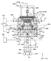
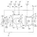
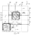
- FIG. 1 schematically shows a configuration of an exposure apparatus 100 according to the first embodiment.
- the exposure apparatus 100 is a step-and-scan projection exposure apparatus, a so-called scanner.
- a projection optical system PL is provided.
- a direction parallel to the optical axis AX of the projection optical system PL is a Z-axis direction, and a reticle in a plane perpendicular to the Z-axis direction.
- the direction in which the wafer is relatively scanned is the Y-axis direction
- the direction orthogonal to the Z-axis and the Y-axis is the X-axis direction
- the rotation (tilt) directions around the X-axis, Y-axis, and Z-axis are ⁇ x, ⁇ y, And the ⁇ z direction will be described.
- the exposure apparatus 100 includes an illumination system 10, a reticle stage RST, a projection unit PU, a stage apparatus 50 having a wafer stage WST and a measurement stage MST, a control system for these, and the like.
- wafer W is placed on wafer stage WST.
- the illumination system 10 includes, for example, a light source, an illumination uniformizing optical system having an optical integrator, and a reticle blind (both not shown) as disclosed in, for example, US Patent Application Publication No. 2003/0025890. And an optical system.
- the illumination system 10 illuminates the slit-shaped illumination area IAR on the reticle R defined by the reticle blind (masking system) with illumination light (exposure light) IL with a substantially uniform illuminance.
- ArF excimer laser light (wavelength 193 nm) is used as the illumination light IL.
- reticle stage RST On reticle stage RST, reticle R on which a circuit pattern or the like is formed on its pattern surface (lower surface in FIG. 1) is fixed, for example, by vacuum suction.
- the reticle stage RST can be slightly driven in the XY plane by a reticle stage drive system 11 (not shown in FIG. 1, refer to FIG. 10) including a linear motor, for example, and also in the scanning direction (left and right direction in FIG. 1). In the Y-axis direction) at a predetermined scanning speed.
- Position information in the XY plane of reticle stage RST (including information on the position in the ⁇ z direction (hereinafter also referred to as ⁇ z rotation (or ⁇ z rotation amount) or yawing (or yawing amount) as appropriate)) is reticle laser interference.
- a meter hereinafter referred to as “reticle interferometer” 116
- a movable mirror 15 (actually, a Y movable mirror (or retroreflector) having a reflective surface orthogonal to the Y-axis direction and a reflective surface orthogonal to the X-axis direction) For example, with a resolution of about 0.25 nm.
- the measurement value of reticle interferometer 116 is sent to main controller 20 (not shown in FIG. 1, refer to FIG. 10).
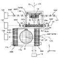
- the projection unit PU is arranged below reticle stage RST in FIG.
- the projection unit PU includes a lens barrel 40 and a projection optical system PL stored in the lens barrel 40.
- the projection optical system PL for example, a refractive optical system including a plurality of optical elements (lens elements) arranged along an optical axis AX parallel to the Z-axis direction is used.
- the projection optical system PL is, for example, double-sided telecentric and has a predetermined projection magnification (for example, 1/4, 1/5, or 1/8).
- the illumination area IAR on the reticle R is illuminated by the illumination system 10
- a reduced image of the circuit pattern of the reticle R in the illumination area IAR passes through the projection optical system PL (projection unit PU), and the second surface of the projection optical system PL ( It is formed in an area (hereinafter also referred to as an exposure area) IA that is conjugated to the illumination area IAR on the wafer W, which is disposed on the image plane side and has a resist (sensitive agent) coated on the surface thereof.
- reticle R is moved relative to illumination area IAR (illumination light IL) in the scanning direction (Y-axis direction) and exposure area IA (illumination light IL).
- illumination area IAR illumination light IL
- exposure area IA illumination light IL
- scanning exposure of one shot area (partition area) on the wafer W is performed, and the pattern of the reticle R is transferred to the shot area.
- a pattern is generated on the wafer W by the illumination system 10, the reticle R, and the projection optical system PL, and the pattern is formed on the wafer W by exposure of the sensitive layer (resist layer) on the wafer W by the illumination light IL. Is formed.
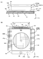
- the exposure apparatus 100 is provided with a local liquid immersion apparatus 8 for performing immersion type exposure.
- the local liquid immersion device 8 includes, for example, a liquid supply device 5, a liquid recovery device 6 (both not shown in FIG. 1, refer to FIG. 10), a liquid supply tube 31A, a liquid recovery tube 31B, a nozzle unit 32, and the like.
- the nozzle unit 32 holds an optical element on the most image plane side (wafer W side) constituting the projection optical system PL, here a lens (hereinafter also referred to as “tip lens”) 191. It is suspended and supported by a main frame (not shown) that holds the projection unit PU so as to surround the lower end portion of the lens barrel 40.
- a main frame not shown
- the lower end surface of the nozzle unit 32 is set substantially flush with the lower end surface of the front lens 191. Further, the nozzle unit 32 is connected to the supply port and the recovery port of the liquid Lq, the lower surface on which the wafer W is disposed and provided with the recovery port, and the supply connected to the liquid supply tube 31A and the liquid recovery tube 31B, respectively. A flow path and a recovery flow path are provided. As shown in FIG.
- the liquid supply pipe 31A and the liquid recovery pipe 31B are inclined by approximately 45 ° with respect to the X-axis direction and the Y-axis direction in plan view (viewed from above), and the center of the projection unit PU has a through (to the exposure with matching the center of the area IA is the optical axis AX, the embodiment of the projection optical system PL) and parallel to the Y axis linear (reference axis) symmetrically arranged with respect to LV 0.
- the liquid supply pipe 31A is connected to the liquid supply apparatus 5 (not shown in FIG. 1, see FIG. 10), and the liquid recovery pipe 31B is connected to the liquid recovery apparatus 6 (not shown in FIG. 1, see FIG. 10).
- the liquid supply device 5 includes a tank for storing the liquid, a pressurizing pump, a temperature control device, a valve for controlling the flow rate of the liquid, and the like.
- the liquid recovery device 6 includes a tank for storing the recovered liquid, a suction pump, a valve for controlling the flow rate of the liquid, and the like.
- the main control device 20 controls the liquid supply device 5 to supply the liquid Lq between the tip lens 191 and the wafer W via the liquid supply pipe 31A and to control the liquid recovery device 6. Then, the liquid Lq is recovered from between the front lens 191 and the wafer W via the liquid recovery tube 31B. At this time, main controller 20 controls liquid supply device 5 and liquid recovery device 6 so that the amount of supplied liquid Lq and the amount of recovered liquid Lq are always equal. Accordingly, a certain amount of liquid Lq (see FIG. 1) is always exchanged and held between the front lens 191 and the wafer W, thereby forming the liquid immersion region 14 (see FIG. 14 and the like). In addition, even when a measurement stage MST described later is positioned below the projection unit PU, the liquid immersion region 14 can be similarly formed between the tip lens 191 and the measurement table.
- pure water that transmits ArF excimer laser light (light having a wavelength of 193 nm) (hereinafter, simply described as “water” unless otherwise required) is used as the liquid.
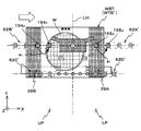
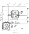
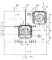
- the stage apparatus 50 includes a wafer stage WST and a measurement stage MST disposed above the base board 12, and a measurement system 200 that measures positional information of these stages WST and MST (see FIG. 10). And a stage drive system 124 (see FIG. 10) for driving the stages WST and MST.
- the measurement system 200 includes an interferometer system 118, an encoder system 150, a surface position measurement system 180, and the like.
- the wafer stage WST and the measurement stage MST are supported on the base board 12 by a non-contact bearing (not shown) fixed to each bottom surface, for example, an air bearing with a clearance of about several ⁇ m.
- the stages WST and MST can be independently driven in the XY plane by a stage driving system 124 (see FIG. 10) including a linear motor, for example.
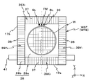
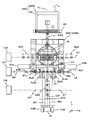
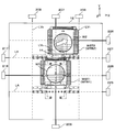
- Wafer stage WST includes a stage main body 91 and a wafer table WTB mounted on stage main body 91.
- Wafer table WTB and stage main body 91 are moved in a direction of six degrees of freedom (X, X) with respect to base board 12 by a drive system including a linear motor and a Z-leveling mechanism (including a voice coil motor) (both not shown).
- Y, Z, ⁇ x, ⁇ y, ⁇ z can be driven.
- a wafer holder (not shown) for holding the wafer W by vacuum suction or the like is provided at the center of the upper surface of the wafer table WTB.
- a circular opening that is slightly larger than the wafer holder is formed in the center outside the wafer holder (wafer mounting area), and has a rectangular outer shape (contour) (liquid repellent).
- Plate) 28 is provided. The surface of the plate 28 is subjected to a liquid repellency treatment with respect to the liquid Lq. The plate 28 is installed so that the entire surface (or part) of the plate 28 is flush with the surface of the wafer W.
- the plate 28 includes a first liquid repellent area 28a having a rectangular outer shape (outline) with the opening formed in the center, and a rectangular frame-shaped second liquid repellent area provided around the first liquid repellent area 28a. 28b.
- first and second liquid repellent regions 28a and 28b are also referred to as first and second water repellent plates 28a and 28b, respectively.
- a measuring plate 30 is provided at the end of the first water repellent plate 28a on the + Y side.
- the measurement plate 30 is provided with a reference mark FM at the center, and a pair of aerial image measurement slit patterns (slit-like measurement patterns) SL so as to sandwich the reference mark FM. Then, corresponding to each aerial image measurement slit pattern SL, a light transmission system (not shown) for guiding the illumination light IL transmitted therethrough to the outside of the wafer stage WST (light receiving system provided in the measurement stage MST described later). ) Is provided.
- Y scales 39Y 1 and 39Y 2 are respectively formed on one side and the other side of the upper surface in the X-axis direction (left and right direction in FIG. 2).
- Each of the Y scales 39Y 1 and 39Y 2 has a grid line 38 having a longitudinal direction in the X axis direction, for example, arranged along a direction (Y axis direction) parallel to the Y axis at a predetermined pitch.
- a reflection type grating for example, a diffraction grating).
- X scales 39X 1 and 39X 2 are respectively formed in regions on one side and the other side of the upper surface of the second water repellent plate 28b in the Y-axis direction (the vertical direction in FIG. 2).
- Each of the X scales 39X 1 and 39X 2 has, for example, lattice lines 37 having a longitudinal direction in the Y-axis direction arranged along a direction (X-axis direction) parallel to the X-axis at a predetermined pitch.
- a reflection type grating for example, a diffraction grating).
- Each scale is produced by, for example, ticking the diffraction grating on a thin glass plate at a pitch between 138 nm and 4 ⁇ m, for example, 1 ⁇ m pitch.
- These scales are covered with the liquid repellent film (water repellent film) described above.
- the pitch of the lattice is shown much wider than the actual pitch.
- the diffraction grating may be covered with a glass plate having a low thermal expansion coefficient having water repellency so that the surface thereof is the same height (surface position) as the surface of the wafer.
- the glass plate a glass plate having the same thickness as the wafer, for example, 1 mm thick can be used.
- a positioning pattern (not shown) for determining the relative position between the encoder head and the scale, which will be described later, is provided near the end of each scale.
- This positioning pattern is composed of, for example, grid lines having different reflectivities.
- reflecting surface 17a and reflecting surface 17b used in an interferometer system to be described later are formed.
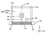
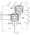
- the measurement stage MST includes a stage main body 92 that is driven in an XY plane by a linear motor (not shown) and the like, and a measurement table MTB mounted on the stage main body 92.
- the measurement stage MST is configured to be driven in at least three degrees of freedom (X, Y, ⁇ z) with respect to the base board 12 by a drive system (not shown).
- a stage drive system 124 including a drive system for wafer stage WST and a drive system for measurement stage MST.
- the measurement table MTB (and the stage main body 92) is provided with various measurement members.
- this measuring member for example, as shown in FIG. 3, an illuminance unevenness sensor 94, an aerial image measuring device 96, a wavefront aberration measuring device 98, an illuminance monitor (not shown), and the like are provided.
- the stage main body 92 is provided with a pair of light receiving systems (not shown) in an arrangement facing the above pair of light sending systems (not shown).
- each aerial image measurement slit pattern SL of measurement plate 30 on wafer stage WST is measured in a state where wafer stage WST and measurement stage MST are close to each other within a predetermined distance in the Y-axis direction (including a contact state).
- An aerial image measuring device 45 (see FIG. 10) is configured in which the transmitted illumination light IL is guided by each light transmission system (not shown) and received by a light receiving element of each light receiving system (not shown) in the measurement stage MST.
- a fiducial bar (hereinafter abbreviated as “FD bar”) 46 extends in the X-axis direction on the ⁇ Y side end face of the measurement table MTB.
- the FD bar 46 is kinematically supported on the measurement stage MST by a full kinematic mount structure. Since the FD bar 46 is a prototype (measurement standard), an optical glass ceramic having a low thermal expansion coefficient, for example, Zerodure (trade name) manufactured by Schott is used as the material.
- Reference gratings (for example, diffraction gratings) 52 having a periodic direction in the Y-axis direction are formed in the vicinity of one end and the other end in the longitudinal direction of the FD bar 46 in a symmetrical arrangement with respect to the center line CL. .
- a plurality of reference marks M are formed on the upper surface of the FD bar 46. As each reference mark M, a two-dimensional mark having a size detectable by a primary alignment system and a secondary alignment system described later is used.
- the surface of the FD bar 46 and the surface of the measurement table MTB are also covered with a liquid repellent film (water repellent film).
- the reflection surface 19a and the reflection surface 19b similar to the wafer table WTB are formed on the + Y side end surface and the ⁇ X side end surface of the measurement table MTB (see FIG. 3).
- a predetermined distance from the center of the projection unit PU (the optical axis AX of the projection optical system PL) is on the ⁇ Y side on the reference axis LV 0 described above.
- a primary alignment system AL1 having a detection center at a position is provided.
- Primary alignment system AL1 is fixed to the lower surface of the main frame (not shown).
- Secondary alignment systems AL2 1 , AL2 2 , AL2 3 , AL2 4 having detection centers arranged almost symmetrically with respect to the reference axis LV 0 on one side and the other side in the X axis direction across the primary alignment system AL1 are provided.
- the secondary alignment systems AL2 1 to AL2 4 are fixed to the lower surface of the main frame (not shown) via a movable support member (not shown), and using drive mechanisms 60 1 to 60 4 (see FIG. 10).
- the relative positions of these detection areas can be adjusted with respect to the X-axis direction.
- a straight line (reference axis) LA parallel to the X axis passing through the detection center of the primary alignment system AL1 shown in FIG. 6 and the like coincides with the optical axis of the measurement beam B6 from the interferometer 127 described later.
- each alignment system (AL1, AL2 1 to AL2 4 ), for example, an image processing type FIA (Field Image Alignment) system is used. Imaging signals from the alignment systems AL1, AL2 1 to AL2 4 are supplied to the main controller 20 through a signal processing system (not shown).
- FIA Field Image Alignment
- interferometer system 118 that measures position information of wafer stage WST and measurement stage MST will be described.
- interferometer system 118 includes Y interferometer 16, X interferometers 126, 127, and 128, and Z interferometers 43A and 43B for measuring the position of wafer stage WST, and the positions of measurement stage MST.
- a Y interferometer 18 for measurement and an X interferometer 130 are included.
- the Y interferometer 16 and the three X interferometers 126, 127, and 128 have interferometer beams (length measuring beams) B4 (B4 1 , B4 2 ) and B5 (B5 1 ) on the reflecting surfaces 17a and 17b of the wafer table WTB, respectively. , B5 2 ), B6 and B7.
- the Y interferometer 16 and the three X interferometers 126, 127, and 128 receive the reflected light, measure the position information of the wafer stage WST in the XY plane, and use the measured position information as the main information. This is supplied to the control device 20.
- the X interferometer 126 passes through the optical axis AX of the projection optical system PL (in this embodiment, also coincides with the center of the exposure area IA described above) and is a straight line (reference axis LH (FIG. 5) parallel to the X axis.
- the reflection surface 17b is irradiated with at least three length measuring beams parallel to the X axis including a pair of length measuring beams B5 1 and B5 2 symmetrical with respect to the above)).
- the Y interferometer 16 reflects at least three measurement beams parallel to the Y axis, including a pair of measurement beams B4 1 , B4 2 , and B3 (see FIG.
- main controller 20 determines the position in the ⁇ x direction (hereinafter referred to as “X” and “Y”) of wafer table WTB (wafer stage WST) based on the measurement results of Y interferometer 16 and X interferometer 126 or 127.
- ⁇ x rotation (or ⁇ x rotation amount), or pitching (or pitching amount) as appropriate, position in the ⁇ y direction (hereinafter, as appropriate, ⁇ y rotation (or ⁇ y rotation amount), or rolling (or rolling amount). ) And ⁇ z rotation (ie yaw amount) can also be calculated.
- a movable mirror 41 having a concave reflecting surface is attached to the side surface of the stage body 91 on the ⁇ Y side.
- the movable mirror 41 is set to have a length in the X-axis direction that is longer than the reflection surface 17a of the wafer table WTB.
- a pair of Z interferometers 43A and 43B are provided to face the movable mirror 41 (see FIGS. 1 and 4).
- the Z interferometers 43A and 43B irradiate two length measuring beams B1 and B2 to the fixed mirrors 47A and 47B fixed to, for example, a main frame (not shown) that supports the projection unit PU via the movable mirror 41, respectively.
- each reflected light is received and the optical path length of length measuring beam B1, B2 is measured.
- main controller 20 calculates the position of wafer stage WST in the four degrees of freedom (Y, Z, ⁇ y, ⁇ z) direction.
- the position in the XY plane (including rotation information in the ⁇ z direction) of wafer stage WST is mainly measured using an encoder system described later.
- Interferometer system 118 is used when wafer stage WST is located outside the measurement area of the encoder system (for example, in the vicinity of unloading position UP and loading position LP shown in FIG. 5 and the like). Further, it is used as an auxiliary when correcting (calibrating) long-term fluctuations in the measurement results of the encoder system (for example, due to deformation of the scale over time) or for backup when the output of the encoder system is abnormal.
- interferometer system 118 and an encoder system may be used together to control the position of wafer stage WST (wafer table WTB).
- the Y interferometer 18 and the X interferometer 130 of the interferometer system 118 irradiate the reflection surfaces 19a and 19b of the measurement table MTB with interferometer beams (measurement beams), respectively.
- position information of the measurement stage MST for example, including at least the position in the X-axis and Y-axis directions and the rotation information in the ⁇ z direction
- the measurement result is sent to the main controller 20. Supply.
- the main configuration of the encoder system 150 is disclosed in, for example, US Patent Application Publication No. 2008/0088843.
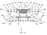
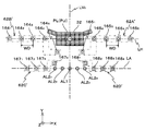
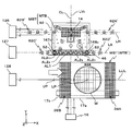
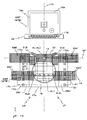
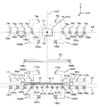
- head units 62A, 62B, 62C, and 62D are provided on the + X side, + Y side, -X side of the nozzle unit 32, and -Y side of the primary alignment system AL1.
- head units 62E and 62F are provided on the ⁇ Y side of the head units 62C and 62A, respectively, and at substantially the same Y position as the primary alignment system AL1.
- the head units 62A to 62F are fixed in a suspended state to a main frame (not shown) that holds the projection unit PU via support members.
- the head unit 62A is arranged on the + X side of the nozzle unit 32, and a plurality of (here, four) head units 62A are arranged on the aforementioned reference axis LH along the X axis direction at intervals WD.
- Y heads 65 2 to 65 5 and a Y head 65 1 disposed at a position on the ⁇ Y side of the nozzle unit 32 that is a predetermined distance away from the reference axis LH in the ⁇ Y direction.
- the distance between the Y heads 65 1 and 65 2 in the X-axis direction is also set substantially equal to WD.
- the head unit 62 ⁇ / b> C is configured symmetrically with the head unit 62 ⁇ / b> A and is disposed symmetrically with respect to the reference axis LV 0 described above.
- the head unit 62C includes Y heads 65 5 to 65 1 and five Y heads 64 1 to 64 5 arranged symmetrically with respect to the reference axis LV 0 .
- Y heads 65 1 to 65 5 and 64 1 to 64 5 are also referred to as Y heads 65 and 64, respectively.
- the head unit 62A uses the Y scale 39Y 1 described above to measure a Y-axis position (Y position) of the wafer stage WST (wafer table WTB) in a multi-lens (here 5 eyes) Y linear encoder ( Hereinafter, 70A (refer to FIG. 10) is configured as appropriate.
- the head unit 62C uses the above-described Y scale 39Y 2 to measure the Y position of the wafer stage WST (wafer table WTB), which is a multi-lens (here, 5 eyes) Y encoder 70C (see FIG. 10). Configure.
- the adjacent Y heads (more precisely, the measurement beam emitted by each Y head).
- the distance WD in the X-axis direction between the irradiation points on the scale) is set to be slightly narrower than the width in the X-axis direction (more precisely, the length of the grid line 38) of the Y scales 39Y 2 and 39Y 1 . Accordingly, at the time of exposure, at least one of the five Y heads 65 j and 64 i always faces the corresponding Y scale 39Y 1 and 39Y 2 .
- the head unit 62B is arranged on the + Y side of the nozzle unit 32 (projection unit PU), and a plurality of head units 62B arranged on the reference axis LV 0 at intervals WD along the Y-axis direction.
- four X heads 66 5 to 66 8 are provided.
- the head unit 62D includes a plurality of (here, four) X heads 66 1 to 66 4 disposed on the ⁇ Y side of the primary alignment system AL1 and disposed on the reference axis LV 0 at an interval WD.
- X heads 66 1 to 66 8 will also be referred to as X head 66 as appropriate.
- the head unit 62B uses the above-described X scale 39X 1 to measure the position (X position) of the wafer stage WST (wafer table WTB) in the X axis direction (multiple eyes (here, four eyes) X linear encoder). (Hereinafter abbreviated as “X encoder” or “encoder” as appropriate) 70B (see FIG. 10). Further, the head unit 62D uses the above-described X scale 39X 2 to measure the X position of the wafer stage WST (wafer table WTB), and a multi-lens (here, four eyes) X linear encoder 70D (see FIG. 10). Configure.
- the head unit 62B, 62D are of the four X heads 66 1-66 4 66 5-66 8 provided respectively, the X heads 66 adjacent (more precisely, the irradiation on the scale of the X head emits the measurement beam
- the interval WD in the Y-axis direction of the dots is set to be narrower than the width of the X scales 39X 1 and 39X 2 in the Y-axis direction (more precisely, the length of the lattice line 37). Therefore, at the time of exposure or wafer alignment, at least one of the four X heads 66 included in the head units 62B and 62D, that is, the eight X heads 66, always corresponds to the corresponding X scale 39X 1 or opposed to the 39X 2.
- the distance between the most + Y side X heads 66 4 of the most -Y side of the X heads 66 5 and the head unit 62D of the head unit 62B is the movement of the Y-axis direction of wafer stage WST, between the two X heads
- the width of the wafer table WTB is set to be narrower than the width in the Y-axis direction so that it can be switched (connected).
- the head unit 62E is arranged on the ⁇ X side of the secondary alignment system AL2 1 , and has three Y heads 67 1 to 67 1 arranged on the above-described reference axis LA at almost the same interval as the interval WD. 67 3, a reference axis Y heads 67 4 arranged in the secondary alignment systems AL2 1 on the + Y side a predetermined distance away in the + Y direction from the LA, and a.
- the distance in the X-axis direction between the Y heads 67 3 and 67 4 is also set to WD.
- Y heads 67 1 to 67 4 are also referred to as Y head 67 as appropriate.
- the head unit 62F is symmetrical with the head unit 62E with respect to the reference axis LV 0 described above, and the four Y heads 68 1 to 68 1 are arranged symmetrically with respect to the four Y heads 67 4 to 67 1 and the reference axis LV 0. Has four .
- the Y heads 68 1-68 4 as appropriate, also described as Y heads 68.
- At the time of an alignment operation described later, at least one of the Y heads 67 p and 68 q (p, q 1 to 4) faces the Y scales 39Y 2 and 39Y 1 .
- the Y position (and ⁇ z rotation) of wafer stage WST is measured by Y heads 67 p and 68 q (that is, Y encoders 70E and 70F constituted by Y heads 67 p and 68 q ).
- the Y positions of the FD bar 46 are measured at the positions of the respective reference gratings 52 by the Y heads 67 3 and 68 2 that are opposed to the reference gratings 52 and opposed to the pair of reference gratings 52, respectively.
- the encoder constituted by the Y heads 67 3 and 68 2 respectively facing the pair of reference grids 52 will be referred to as Y encoders 70E 2 and 70F 2
- the above-described Y scales 39Y 2 and 39Y are used for identification.
- the Y encoders 70E and 70F configured by the Y heads 67 and 68 facing 1 are referred to as Y encoders 70E 1 and 70F 1 .
- the measurement values of the encoders 70A to 70F described above are supplied to the main control device 20, and the main control device 20 has three of the encoders 70A to 70D or three of the 70B, 70D, 70E 1 and 70F 1 . Based on the measurement value, the position of wafer stage WST in the XY plane is controlled, and based on the measurement value of encoders 70E 2 and 70F 2 , rotation (yawing) of FD bar 46 (measurement stage MST) in the ⁇ z direction is performed. Control.
- the measurement stage MST is not shown, and a liquid immersion area formed by the water Lq held between the measurement stage MST and the tip lens 191 is indicated by reference numeral 14.
- symbols UP and LP are set symmetrically with respect to the reference axis LV 0 , an unloading position at which the wafer is unloaded on the wafer table WTB, and the wafer is loaded onto the wafer table WTB. Each loading position is shown. Note that the unloading position UP and the loading position LP may be the same position.
- an irradiation system 90a and a light receiving system 90b having the same configuration as that disclosed in US Pat. No. 5,448,332, for example.
- An oblique incidence type multi-point focal position detection system (hereinafter abbreviated as “multi-point AF system”) 90 is provided.
- the irradiation system 90a is disposed on the + Y side of the ⁇ X end of the head unit 62E described above, and light is received on the + Y side of the + X end of the head unit 62F while facing this.
- a system 90b is arranged.
- the multipoint AF system 90 is fixed to the lower surface of the main frame that holds the projection unit PU described above.
- a plurality of detection points of the multi-point AF system 90 (90a, 90b) are arranged at predetermined intervals along the X-axis direction on the surface to be detected.
- N M / 2 2).
- a plurality of detection points irradiated with the detection beam are not individually illustrated, and are long and narrow detection areas (beam areas) AF extending in the X-axis direction between the irradiation system 90a and the light receiving system 90b. It is shown.
- this detection area AF has a length in the X-axis direction that is set to be approximately the same as the diameter of the wafer W, the wafer W is scanned almost once in the Y-axis direction, so that the entire surface of the wafer W is almost completely Z-axis direction.
- Position information (surface position information) can be measured.
- the multipoint AF system 90 (90a, 90b) in the vicinity of both end portions of detection area AF of the reference axis LV 0 with respect to symmetrical arrangement, the surface position sensors for measuring the pair of Z position Heads (hereinafter abbreviated as “Z head”) 72a, 72b, and 72c, 72d are provided.
- the Z heads 72a to 72d are fixed to the lower surface of the main frame (not shown).
- Z heads 72a to 72d for example, an optical displacement sensor head similar to an optical pickup used in a CD drive device or the like is used.
- Z heads 72a to 72d irradiate wafer table WTB with a measurement beam from above, receive the reflected light, and measure the surface position of wafer table WTB at the irradiation point.
- a configuration is adopted in which the measurement beam of the Z head is reflected by the reflection type diffraction grating constituting the Y scales 39Y 1 and 39Y 2 described above.
- the three outer Z heads 76 3 to 76 5 and 74 1 to 74 3 belonging to the head units 62A and 62C are arranged in parallel to the reference axis LH at a predetermined distance in the + Y direction from the reference axis LH. Has been.
- head units 62A on the + Y side of the innermost Z heads 76 1, 74 5 projection unit PU belonging to each of 62C, 2 remaining Z heads 76, 74 4 each Y heads 65 2, 64 4 - Arranged on the Y side.
- the five Z heads 76 j and 74 i belonging to the head units 62A and 62C are arranged symmetrically with respect to the reference axis LV 0 .
- a head of an optical displacement sensor similar to the Z heads 72a to 72d described above is employed as each of the Z heads 76 j and 74 i .
- the adjacent Z head (more precisely, the irradiation point on the scale of the measurement beam emitted by each Z head) in the X-axis direction is The distance WD in the X-axis direction between the Y heads 65 and 64 is set equal. Accordingly, at the time of exposure, at least one of each of the five Z heads 76 j and 74 i is always set to the corresponding Y scale 39Y 1 and 39Y 2 , similarly to the Y heads 65 j and 64 i. opposite.
- the Z heads 72a to 72d, 74 1 to 74 5 , and 76 1 to 76 5 described above are connected to the main controller 20 via the signal processing / selecting device 160 as shown in FIG.
- the main controller 20 selects an arbitrary Z head from among the Z heads 72a to 72d, 74 1 to 74 5 , and 76 1 to 76 5 via the signal processing / selecting device 160, and sets the operating state.
- the surface position information detected by the Z head is received via the signal processing / selection device 160.
- Z heads 72a ⁇ 72d, 74 1 ⁇ 74 5, 76 and 1-76. 5 the position information of the tilt direction and a signal processing and selection device 160 with respect to the Z-axis direction and the XY plane of wafer stage WST
- a surface position measurement system 180 that measures the above is configured.
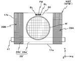
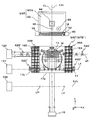
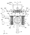
- a peripheral exposure unit extending in the X-axis direction between the detection area (beam area) AF of the multipoint AF system and the head units 62C and 62A. 51 is arranged.
- the peripheral exposure unit 51 is supported in a suspended state on a lower surface of a main frame (not shown) via a support member (not shown).
- the peripheral exposure unit 51 includes a light source (not shown) that emits light having substantially the same wavelength as the illumination light IL, and a peripheral exposure active mask (hereinafter, abbreviated as an active mask as appropriate) 51a on which light from the light source enters. (See FIG. 8).
- the illumination light IL may be guided to the active mask 51a using, for example, an optical fiber.
- the length of the peripheral exposure unit 51 (active mask 51a) is set to be somewhat longer than the diameter of the wafer W, as shown in FIG. As shown in FIG. 8 as an example, the active mask 51a has a pair of variable shaping masks VM1 and VM2 at both ends in the X-axis direction.
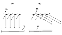
- a micromirror array including a plurality of micromirrors M ij (see FIGS. 9A and 9B) arranged in a matrix in the XY plane.
- a movable micromirror is formed by MEMS technology on an integrated circuit made by a CMOS process.
- Each micromirror M ij tilts a mirror surface (reflection surface) around a predetermined axis (for example, an axis coinciding with the diagonal of the micromirror) within a predetermined angular range, ⁇ ⁇ ( ⁇ is, for example, 3 degrees (or 12 degrees)).
- each variable shaping mask includes a base substrate, a movable microphone mirror M ij formed on the substrate, and an electrode for turning each micro mirror on and off.
- Each micromirror M ij reflects, as an example, a state (or posture) of reflecting light from the light source toward the wafer W as shown in FIG. B) is set to one of the states (or postures) in which light from the light source is reflected in a predetermined direction that does not enter the wafer W.
- the former is referred to as an on state (or an on posture) of the micromirror M ij
- the latter is referred to as an off state (or an off posture) of the micromirror M i, j .
- the main controller 20 individually controls each micromirror M ij to either the on state (or on posture) or the off state (or off posture). Therefore, according to the peripheral exposure unit 51 of the present embodiment, the wafer stage WST is moved in the Y-axis direction while the center of the wafer W in the X-axis direction and the center of the peripheral exposure unit 51 in the longitudinal direction substantially coincide with each other. Thus, an arbitrary pattern can be formed by exposing an arbitrary position in the vicinity of both ends of the wafer W in the X-axis direction. That is, the peripheral exposure unit 51 can form two irradiation regions for peripheral exposure that are separated in the X-axis direction, and the position thereof is variable at least in the X-axis direction.
- FIG. 10 shows the main configuration of the control system of the exposure apparatus 100.
- This control system is mainly configured of a main control device 20 composed of a microcomputer (or a workstation) for overall control of the entire apparatus.
- various sensors provided on the measurement stage MST such as the illuminance unevenness sensor 94, the aerial image measuring device 96, and the wavefront aberration measuring device 98 described above, are collectively shown as a sensor group 99.
- the main controller 20 controls the opening and closing of the valves of the liquid supply device 5 and the liquid recovery device 6 of the local liquid immersion device 8 as described above, and the leading end lens of the projection optical system PL. 191 is always filled with water.
- the control of the liquid supply device 5 and the liquid recovery device 6 is omitted.
- the following description of the operation will be made with reference to a number of drawings, and the same members may or may not be labeled with the same members for each drawing. In other words, although the reference numerals described in the drawings are different, the drawings have the same configuration regardless of the presence or absence of the reference numerals. The same applies to each drawing used in the description so far.
- FIG. 11 a plan view of the wafer W is shown.
- the shot area Sj is a two-shot area where two identical devices (chips) are formed.
- 16 shot areas (S2, S4, S6, S18, S20, S22, S24, S26, S51, S53, S55, S57, S59, S71, S73, and S75 that are blackened in FIG. 12 are used.
- three shot areas are first alignment shot areas, and five shot areas (S51, S53, S55, S57, S59) are second alignment shot areas, Five shot regions (S18, S20, S22, S24, S26) are third alignment shot regions, and three shot regions (S2, S4, S6) are force alignment shot regions.
- peripheral shots S1, S7, S8, S16, S17, S27, S50, S60, S61, S69, S70, S76
- the half area on the edge side of the wafer W (S1a, S7a, S8a, S16a, S17a, S27a, S50a, S60a, S61a, S69a, S70a, S76a) is a peripheral exposure target area (hereinafter referred to as a peripheral exposure area). It has become.
- FIG. 14 shows a state in which step-and-scan exposure is performed on wafer W placed on wafer stage WST.
- wafer stage WST is moved to the scanning start position (acceleration start position) for exposure of each shot area on wafer W based on the result of wafer alignment (EGA: Enhanced Global Alignment) performed before the start. It is performed by repeating the movement between the moving shots and the scanning exposure in which the pattern formed on the reticle R is transferred to each shot area by the scanning exposure method. Further, the exposure is performed in the order from the shot area located on the ⁇ Y side on the wafer W to the shot area located on the + Y side. Note that the liquid immersion region 14 is formed between the projection unit PU and the wafer W.
- main controller 20 causes wafer stage WST to have a position in the XY plane (including the position in the ⁇ z direction ( ⁇ z rotation)) of two Y encoders 70A and 70C and two X encoders 70B and 70D. Control is performed based on the measurement results of a total of three encoders.
- the two X encoders 70B and 70D are constituted by two X heads 66 facing the X scales 39X 1 and 39X 2 respectively, and the two Y encoders 70A and 70C are the Y scales 39Y 1 and 39Y 2 .
- the Y heads 65 and 64 are opposed to each other.
- the Z position and ⁇ y rotation (rolling) of wafer stage WST are respectively controlled by Z heads 74 i , belonging to head units 62C and 62A, which face the X-axis direction one side and the other side of the wafer table WTB surface, respectively. It is controlled based on the measured value of 76 j .
- the ⁇ x rotation (pitching) of wafer stage WST is controlled based on the measurement value of Y interferometer 16.
- Z heads 74 i, 76 j In the case where three or more Z heads including Z head 74 i, 76 j on the surface of second water repellent plate 28b of wafer table WTB is opposed, Z heads 74 i, 76 j, and the other one Z Based on the measurement value of the head, it is also possible to control the position of wafer stage WST in the Z-axis direction, ⁇ y rotation (rolling), and ⁇ x rotation (pitching). In any case, control of the position of the wafer stage WST in the Z-axis direction, ⁇ y rotation, and ⁇ x rotation (that is, focus / leveling control of the wafer W) is performed based on the result of focus mapping performed in advance. .
- main controller 20 executes position (Z, ⁇ y) control of wafer stage WST using Z heads 74 3 and 76 3 .
- Z heads 74 3 and 76 3 deviate from the corresponding Y scale, and instead, Z heads 74 4 and 76 4 (Shown in a circle) are opposed to the Y scales 39Y 2 and 39Y 1 , respectively. Therefore, main controller 20 switches to stage control using Z heads 74 4 and 76 4 .
- main controller 20 performs stage control by constantly switching the encoder and Z head to be used according to the position coordinates of wafer stage WST.
- the X position and ⁇ z rotation amount (yawing amount) of wafer stage WST are converted to Y position and ⁇ x rotation using Y interferometer 16 using X interferometers 126, 127, or 128 constituting interferometer system 118.
- the Z position, the Z position, the ⁇ y rotation amount, and the ⁇ z rotation amount are measured using the Z interferometers 43A and 43B.
- any one of X interferometers 126, 127, and 128 is used according to the Y position of wafer stage WST.
- an X interferometer 126 is used as shown in FIG.
- the measurement result of the interferometer system 118 excludes the pitching amount ( ⁇ x rotation amount), either supplementarily, at the time of backup described later, or when measurement by the encoder system 150 and / or the surface position measurement system 180 cannot be performed. It is used for position control of wafer stage WST.
- main controller 20 drives wafer stage WST toward unload position UP.
- the wafer stage WST and the measurement stage MST which are separated from each other during the exposure, come into contact with each other with a separation distance of about 300 ⁇ m therebetween, and shift to the scram state.
- the ⁇ Y side surface of FD bar 46 on measurement table MTB and the + Y side surface of wafer table WTB come into contact with or approach each other.
- both stages WST and MST move in the ⁇ Y direction, so that the liquid immersion region 14 formed under the projection unit PU moves onto the measurement stage MST.
- FIGS. 15 and 16 show the state after the movement.
- wafer stage WST releases the scrum state with measurement stage MST and moves to unloading position UP.
- main controller 20 unloads wafer W on wafer table WTB.
- main controller 20 drives wafer stage WST in the + X direction to move it to loading position LP, and loads the next wafer W onto wafer table WTB.
- main controller 20 adjusts the position of FD bar 46 supported by measurement stage MST in the XY plane, baseline measurement of four secondary alignment systems AL2 1 to AL2 4 , Execute Sec-BCHK (secondary baseline check). Sec-BCHK is performed at intervals for each wafer exchange.
- the Y encoders 70E 2 and 70F 2 described above are used.
- main controller 20 drives wafer stage WST to position reference mark FM on measurement plate 30 within the detection field of primary alignment system AL1, as shown in FIG. 17, and alignment systems AL1, AL2
- Pri-BCHK Primary Baseline Check
- two Y heads 68 2 and 67 3 and one X head 66 1 are respectively connected to Y scales 39Y 1 and 39Y 2. and come to face the X scale 39X 2. Therefore, main controller 20 switches from interferometer system 118 to stage control using encoder system 150 (encoders 70E 1 , 70F 1 , 70D). Interferometer system 118 is used again as an auxiliary, except for measuring the amount of ⁇ x rotation of wafer stage WST. Of the three X interferometers 126, 127, and 128, the X interferometer 127 is used.
- main controller 20 manages the position of wafer stage WST based on the measurement values of the three encoders described above, and moves toward the position where alignment marks attached to the three first alignment shot areas are detected. Starts moving the wafer stage WST in the + Y direction.
- main controller 20 stops wafer stage WST.
- the main controller 20 operates (turns on) the Z heads 72a to 72d when all or a part of the Z heads 72a to 72d face the wafer table WTB or at a point before that. Measurement of the Z position and tilt amount ( ⁇ y rotation amount) of wafer stage WST is started.
- main controller 20 uses primary alignment system AL1, secondary alignment systems AL2 2 and AL2 3 to detect the alignment marks attached to the three first alignment shot areas almost simultaneously and individually. (See the star mark in FIG. 18), the detection results of the three alignment systems AL1, AL2 2 and AL2 3 and the measurement values of the three encoders at the time of detection are associated with each other and stored in a memory (not shown).
- the transition to the contact state (or proximity state) between the measurement stage MST and the wafer stage WST is completed at the position where the alignment mark in the first alignment shot region is detected.
- Main controller 20 moves both stages WST and MST in the + Y direction in the contact state (or proximity state) (step movement toward the position where alignment marks attached to the five second alignment shot areas are detected) ) Is started.
- main controller 20 irradiates wafer table WTB with the detection beam of multipoint AF system (90a, 90b) as shown in FIG. To start. As a result, a multi-point AF detection area is formed on wafer table WTB.
- main controller 20 sets center of wafer table WTB on reference axis LV 0.
- the measured values of the Z heads 72a, 72b, 72c, 72d (the surface position information at one end and the other end of the wafer table WTB) in the state where the lines match, and the multipoint AF system (90a, 90b) )
- the detection result surface position information
- the liquid immersion region 14 is formed on the upper surface of the FD bar 46.
- main controller 20 determines in the XY plane of wafer stage WST based on the measured values of X head 66 2 (X linear encoder 70D) and Y linear encoders 70E 1 and 70F 1 facing X scale 39X 2 . The position is controlled.
- main controller 20 again moves both stages WST and MST in the + Y direction in the contact state (or in the proximity state) after the detection of the alignment marks attached to the five second alignment shot areas is completed. Simultaneously with the start, as shown in FIG. 20, position information (surface position information) on the surface of the wafer W in the Z-axis direction is detected using the Z heads 72a to 72d and the multipoint AF system (90a, 90b). Start focus mapping.
- main controller 20 measures by Y linear encoders 70E 1 and 70F 1 .
- Y linear encoders 70E 1 and 70F 1 By controlling on / off of each micromirror M ij constituting the two variable forming masks VM1, VM2 of the peripheral exposure unit 51 according to the Y position of the wafer stage WST, FIG. As shown in FIG. 25B and FIG. 25C, the peripheral exposure regions S70a and S76a, S61a and S69a, S50a and S60a are sequentially exposed.
- main controller 20 may expose each peripheral exposure region entirely using peripheral exposure unit 51 or may form a predetermined pattern.
- main controller 20 provides an optical axis for projection optical system PL of wafer stage WST. Wafer stage with reference to surface position information measured by Z heads 72a, 72b, 72c, 72d without switching the Z head used for controlling the position (Z position) with respect to the direction to Z heads 74 i , 76 j In the state where the Z position control of WST (measurement plate 30) is continued, the following second half of the focus calibration is performed.
- main controller 20 controls the position (Z position) in the optical axis direction of projection optical system PL of measurement plate 30 (wafer stage WST) on the basis of the surface position information measured by Z heads 72a to 72d.
- the aerial image of the measurement mark formed on the mark plate (not shown) on the reticle R or the reticle stage RST using the aerial image measuring device 45 is converted into, for example, the pamphlet of International Publication No. 2005/1224834 (and corresponding to this).
- the best focus position of the projection optical system PL is measured based on the measurement result disclosed in US Patent Application Publication No. 2008/030715).
- Main controller 20 synchronizes with the capture of the output signal from aerial image measurement device 45 during the above Z-direction scan measurement, and surface position information at one end and the other end of wafer table WTB in the X-axis direction.
- the measurement values of the pair of Z heads 74 3 and 76 3 are measured.
- the values of the Z heads 74 3 and 76 3 corresponding to the best focus position of the projection optical system PL are stored in a memory (not shown).
- the position (Z position) of the measurement plate 30 (wafer stage WST) in the optical axis direction of the projection optical system PL on the basis of the surface position information measured by the Z heads 72a to 72d in the latter half of the focus calibration process. This is because the latter half of the focus calibration is performed during the focus mapping described above.
- the main controller 20 performs the following processing of the latter half of the Pri-BCHK before and after the processing of the latter half of the focus calibration. That is, main controller 20 uses, for example, the aerial image measuring device 45, a projected image (aerial image) of a pair of measurement marks on reticle R projected by projection optical system PL.
- main controller 20 uses, for example, the aerial image measuring device 45, a projected image (aerial image) of a pair of measurement marks on reticle R projected by projection optical system PL.
- measurement is performed in a slit-scan aerial image measurement operation using a pair of aerial image measurement slit patterns SL, and the measurement results (XY of wafer table WTB)
- the aerial image intensity corresponding to the position is stored in the memory.
- the position of the XY plane of wafer table WTB is the X head 66 4 facing X scale 39X 2 (encoders 70D), opposite to the Y scales 39Y 1, 39Y 2 2 Control is performed based on the two Y heads 67 3 and 68 2 (encoders 70E 1 and 70F 1 ) (or Y heads 65 j and 64 i (encoders 70A and 70C)).
- main controller 20 calculates the baseline of primary alignment system AL1 based on the result of the first half of Pri-BCHK and the result of the second half of Pri-BCHK. At the same time, the main controller 20 obtains an offset at a representative detection point of the multipoint AF system (90a, 90b) based on the results of the first and second half processes of the focus calibration described above, and stores it in the internal memory. Store. The main controller 20 adds an offset to the mapping information when reading the mapping information obtained as a result of the focus mapping during exposure.
- main controller 20 moves wafer stage WST to its position. While stopping at the position, the measurement stage MST continues to move in the + Y direction as it is. Then, main controller 20 uses five alignment systems AL1, AL2 1 to AL2 4 to detect the alignment marks attached to the five third alignment shot regions almost simultaneously and individually (the star mark in FIG. 22). (See), the detection results of the five alignment systems AL1, AL2 1 to AL2 4 and the measurement values of the three encoders at the time of detection are associated with each other and stored in the internal memory. Also at this point, focus mapping continues.
- measurement stage MST and wafer stage WST shift from contact (or proximity state) to separation state. After shifting to this separated state, main controller 20 stops at that position when measurement stage MST reaches an exposure start standby position where it waits until exposure starts.
- main controller 20 starts moving wafer stage WST in the + Y direction toward a position for detecting alignment marks attached to the three force alignment shots. At this time, the focus mapping is continued. On the other hand, measurement stage MST stands by at the exposure start stand-by position.
- main controller 20 starts Y linear encoder 70E 1 until both stages WST and MST start moving in the + Y direction and reach the position shown in FIG. , 70F 1 , according to the Y position of the wafer stage WST, the micromirrors M ij constituting the two variable forming masks VM1, VM2 of the peripheral exposure unit 51 are individually controlled on and off. As shown in FIGS. 25D and 25E, the peripheral exposure regions S17a and S27a, S8a and S16a are sequentially exposed. Also in this case, main controller 20 may expose each peripheral exposure region entirely using peripheral exposure unit 51 or may form a predetermined pattern.
- main controller 20 immediately stops wafer stage WST, and uses wafers on wafer W using primary alignment system AL1, secondary alignment systems AL2 2 and AL2 3. Alignment marks attached to the three force alignment shot areas are detected almost simultaneously and individually (see the star mark in FIG. 23), and the detection results of the above three alignment systems AL1, AL2 2 and AL2 3 and their detection time Of the four encoders (for example, 70E 1 , 70E 2 , 70B, 70D) are associated with the measured values of the three encoders and stored in a memory (not shown). Even at this time, the focus mapping is continued, and the measurement stage MST remains on standby at the exposure start standby position.
- primary alignment system AL1, secondary alignment systems AL2 2 and AL2 3. Alignment marks attached to the three force alignment shot areas are detected almost simultaneously and individually (see the star mark in FIG. 23), and the detection results of the above three alignment systems AL1, AL2 2 and AL2 3 and their detection time Of the four encoders (for example, 70E 1 , 70E 2 , 70B
- main controller 20 uses the detection results of the total 16 alignment marks thus obtained and the corresponding encoder measurement values, for example, the statistics disclosed in Japanese Patent Application Laid-Open No. 61-044429. Calculation is performed to calculate array information (coordinate values) of all shot areas on the wafer W on the coordinate system defined by the measurement axes of the four encoders 70E 1 , 70E 2 , 70B, and 70D of the encoder system. .
- main controller 20 continues the focus mapping while moving wafer stage WST in the + Y direction again.
- main controller 20 performs two variable moldings of peripheral exposure unit 51 according to the Y position of wafer stage WST, which is measured by Y linear encoders 70E 1 and 70F 1 .
- mask VM1, VM2 by individually controlling the on and off of the micromirrors M ij constituting a, as shown in FIG. 25 (F), successively exposing a peripheral exposure regions S1a and S7a.
- main controller 20 may expose each peripheral exposure region entirely using peripheral exposure unit 51 or may form a predetermined pattern.
- peripheral exposure of the wafer W is completed, and the peripheral exposure regions S1a, S7a, S8a, S16a, S17a, S27a, S50a, S60a, S61a, S69a, S70a, and S76a are exposed as shown in FIG. This is a completed area.
- main controller 20 moves wafer stage WST to a scan start position (exposure start position) for first shot exposure on wafer W.
- main controller 20 moves Z position of wafer stage WST, While maintaining the ⁇ y rotation and the ⁇ x rotation, the Z head used for controlling the Z position and ⁇ y rotation of wafer stage WST is switched from Z heads 72a to 72d to Z heads 74 i and 74 j .
- the main controller 20 performs the step-and-scan method based on the results of the wafer alignment (EGA) described above and the baselines of the five latest alignment systems AL1, AL2 1 to AL2 4 . Exposure is performed by immersion exposure, and a reticle pattern is sequentially transferred to a plurality of shot areas on the wafer W. Thereafter, the same operation is repeated.
- a plurality of detection points are set at predetermined intervals in the X-axis direction while the wafer stage WST moves linearly in the Y-axis direction.
- Surface position information on the surface of the wafer W is detected by the point AF system (90a, 90b), and a plurality of alignment systems AL1, AL2 1 to AL2 4 in which detection areas are arranged in a line along the X-axis direction on the wafer W. Alignment marks whose positions are different from each other are detected, and the peripheral exposure unit 51 performs peripheral exposure of the wafer W.
- wafer stage WST (wafer W) includes a plurality of detection points (detection areas AF) of multipoint AF system (90a, 90b), detection areas of a plurality of alignment systems AL1, AL2 1 to AL2 4 , and peripheral exposure.
- detection points AF detection areas of multipoint AF system
- AL1, AL2 1 to AL2 4 detection areas of a plurality of alignment systems AL1, AL2 1 to AL2 4 , and peripheral exposure.
- the alignment mark detection operation it is possible to significantly improve the throughput as compared with the case where the alignment mark detection operation, the surface position information (focus information) detection operation, and the peripheral exposure operation are performed independently (separately). That is, since the time required for the peripheral exposure operation can be substantially overlapped with the wafer alignment operation time, the peripheral exposure operation hardly reduces the throughput.
- the position information in the XY plane of the wafer table WTB is not affected by air fluctuations or the like by the encoder system 150 including the encoders 70A to 70F and the like that have good short-term measurement stability.
- the surface position measurement system 180 including the Z heads 72a to 72d, 74 1 to 74 5 , 76 1 to 76 5, and the like is capable of accurately measuring the position information in the Z-axis direction orthogonal to the XY plane of the wafer table WTB. It is measured with high accuracy without being affected by air fluctuation.
- both the encoder system 150 and the surface position measurement system 180 directly measure the upper surface of the wafer table WTB, it is possible to control the position of the wafer table WTB, and hence the wafer W, simply and directly. Become.
- the surface position measurement system 180 and the multipoint AF system (90a, 90b) are simultaneously operated by the main controller 20 during the focus mapping described above, and the multipoint AF system (90a, 90b, The detection result of 90b) is converted into data based on the measurement result of the surface position measurement system 180. Therefore, by obtaining this conversion data in advance, the surface position measurement system 180 can only measure the position information in the Z-axis direction of the wafer table WTB and the position information in the tilt direction with respect to the XY plane. The surface position of the wafer W can be controlled without acquiring the surface position information of W. Therefore, in the present embodiment, the focus / leveling control of the wafer W at the time of exposure is performed with high accuracy without any particular problem, although the working distance between the front lens 191 and the surface of the wafer W is narrow. be able to.
- the surface position of the wafer table WTB and hence the wafer W can be controlled with high accuracy, so that high-accuracy exposure with almost no exposure failure due to surface position control errors becomes possible.
- a pattern image can be formed on the wafer W without image blur due to defocusing.
- the arrangement interval in the X-axis direction of the plurality of Y heads 64 and 65 whose measurement direction is the Y-axis direction is narrower than the width of the Y scales 39Y 1 and 39Y 2 in the X-axis direction.
- the arrangement interval in the Y axis direction of the plurality of X heads 66 whose direction is the measurement direction is narrower than the width of the X scales 39X 1 and 39X 2 in the Y axis direction.
- the Y linear encoder 70A that irradiates the Y scale 39Y 1 or 39Y 2 with detection light (beam) while sequentially switching the plurality of Y heads 64 and 65 or Based on the measurement value of 70C, the Y position of wafer table WTB (wafer stage WST) can be measured.
- a plurality of X heads 66 are sequentially switched and detected on X scale 39X 1 or 39X 2 .
- the X position of wafer table WTB (wafer stage WST) can be measured based on the measurement value of X linear encoder 70B or 70D that emits light (beam).
- the alignment system (AL1, AL2 1 to AL 4 ) is separated from the exposure position where the wafer W is exposed (position where the liquid immersion area 14 below the projection unit PU is formed) in the Y-axis direction. ), And the multi-point AF system 90 and the peripheral exposure unit 51 are exemplified, but the present invention is not limited to this.
- one of the alignment system (AL1, AL2 1 to AL2 4 ) and the multipoint AF system 90 may not be arranged at the above position. Even in such a case, the wafer peripheral exposure can be performed in parallel with the wafer stage WST being moved in the Y-axis direction toward the exposure position for the measurement of the wafer by the other measuring apparatus. . Accordingly, the time required for the peripheral exposure can be overlapped with another processing time, so that the throughput can be improved.
- both the alignment system (AL1, AL2 1 to AL2 4 ) and the multipoint AF system (90a, 90b) may not be arranged at the above positions.
- a measuring apparatus that performs some measurement on the wafer is disposed at the same position as the alignment system (AL1, AL2 1 to AL 4 ) and the multipoint AF system (90a, 90b).
- the present invention is not limited to this, and at least one of the Y scales 39Y 1 and 39Y 2 for measuring the position in the Y-axis direction and the X scales 39X 1 and 39X 2 for measuring the position in the X-axis direction is not a pair but only one. Alternatively, it may be provided on wafer table WTB, or at least one of the pair of head units 62A and 62C and the two head units 62B and 62D may be provided. Further, the extending direction of the scale and the extending direction of the head unit are not limited to orthogonal directions such as the X-axis direction and the Y-axis direction in the above-described embodiment, and may be any direction that intersects each other.
- the head units 62A to 62D have a plurality of heads arranged at a predetermined interval.
- the present invention is not limited to this, and the light beam is applied to a region extending in the pitch direction of the Y scale or X scale.
- a single head provided may be employed.
- AL1, AL2 1 to AL2 4 alignment system
- multipoint AF system 90a, 90b
- Z sensor interferometer system 118
- encoder system 70A
- the present invention is not limited to this.
- the present invention can be applied to an exposure apparatus that is not provided with a measurement stage MST or the like.
- the present invention is applicable as long as it includes a wafer stage (moving body) and some other constituent parts among the above constituent parts.
- the peripheral exposure unit 51 is arranged on the projection unit PU side of the alignment system (AL1, AL2 1 to AL 4 ) (and the multipoint AF system (90a, 90b)) is illustrated.
- the peripheral exposure unit may be arranged on the unloading position UP and loading position LP side of the alignment system (AL1, AL2 1 to AL 4 ) (and the multipoint AF system (90a, 90b)). good.
- the wafer stage WST is subjected to the peripheral exposure of the wafer W in the forward path from the loading position LP toward the exposure position (projection unit PU) is exemplified.
- the peripheral exposure may be performed on the return path from the position (projection unit PU) to the unloading position UP, or the peripheral exposure of one wafer may be performed on both the outward path and the return path.
- the peripheral exposure unit 51 capable of irradiating two irradiation areas for peripheral exposure separated in the X-axis direction
- the configuration of the peripheral exposure unit is not limited to this.
- wafer stage WST detects a plurality of detection points (detection areas AF) of multipoint AF system (90a, 90b) and a plurality of alignment systems AL1, AL2 1 to AL2 4 .
- the surface position information of almost the entire surface of the wafer W, the detection of all the alignment marks to be detected on the wafer W, and the wafer W can be obtained simply by linearly passing through the area and below the peripheral exposure unit 51.
- the case where the three operations with the peripheral exposure are completed has been described.
- the present invention is not limited thereto, and at least a part of the peripheral exposure operation may be performed in parallel with the movement of the wafer stage WST (wafer W) from the loading position to the exposure position.
- the throughput can be further improved. That is, it is sufficient that at least a part of the peripheral exposure operation is performed during the movement of the wafer stage WST (wafer W) from the loading position to the exposure position, and the others are not essential.
- the measurement system 200 includes both the interferometer system 118 and the encoder system 150.
- the measurement system is not limited thereto, and the measurement system is one of the interferometer system 118 and the encoder system 150. May contain only.
- FIG. 27 schematically shows a configuration of an exposure apparatus 500 according to the second embodiment.
- the exposure apparatus 500 is a step-and-scan projection exposure apparatus, a so-called scanner.
- the exposure apparatus 500 includes an illumination system 10, a reticle stage RST, a projection unit PU, a stage apparatus 50 having a wafer stage WST and a measurement stage MST, a control system for these, and the like.
- wafer W is placed on wafer stage WST.
- the exposure apparatus 500 is different from the exposure apparatus 100 of the first embodiment except that a wafer table WTB ′ is used instead of the wafer table WTB described above, and the configuration of the encoder system 150 is different.
- the exposure apparatus 100 is configured similarly to the exposure apparatus 100 of the first embodiment. In the following, the description will be focused on the differences, and the same reference numerals are used for the same or equivalent components as those in the first embodiment described above, and the description will be simplified or omitted. Further, for simplification of description, the description of the configuration related to the peripheral exposure and focus / leveling control of the wafer W is omitted.
- the stage apparatus 50 includes a wafer stage WST and a measurement stage MST arranged on the base board 12, as in the first embodiment.
- the stage apparatus 50 further includes a measurement system 200 that measures positional information of both stages WST and MST, a stage drive system 124 that drives both stages WST and MST, and the like (both not shown in FIG. 27, see FIG. 32). It has.
- the measurement system 200 includes an interferometer system 118 and an encoder system 150 as shown in FIG.
- Wafer stage WST includes stage main body 91 and wafer table WTB 'mounted on stage main body 91.
- Wafer table WTB ′ and stage main body 91 are driven in a direction of six degrees of freedom (X, Y, Z, ⁇ x) with respect to base board 12 by a drive system including, for example, a linear motor and a Z / leveling mechanism (including a voice coil motor). , ⁇ y, ⁇ z).
- a wafer holder (not shown) that holds the wafer W by vacuum suction or the like is provided at the center of the upper surface of the wafer table WTB '.
- a plate liquid repellent
- the surface of the plate 28 ' is subjected to a liquid repellency treatment with respect to the liquid Lq.
- the plate 28 ′ is installed so that all or part of the surface thereof is flush with the surface of the wafer W.
- the plate 28 ′ is positioned at the center in the X-axis direction of the wafer table WTB, and the first liquid repellent region 28 a ′ having a rectangular outer shape (contour) in which the above-described circular opening is formed at the center, and the first The wafer table WTB has a pair of rectangular second liquid repellent regions 28b ′ positioned at the + X side end portion and the ⁇ X side end portion of the wafer table WTB with the liquid repellent region 28a ′ interposed therebetween in the X axis direction.
- the first and second liquid repellent regions 28a ′ and 28b ′ are hereinafter referred to as the first and second water repellent plates 28a ′ and 28a, respectively. Also referred to as 28b '.
- a reference mark FM and a pair of aerial image measurement slit patterns (slit-like measurement patterns) SL sandwiching the reference mark FM are formed in the vicinity of the + Y side end of the first water repellent plate 28a ′.
- a plate 30 is provided.
- the illumination light IL passing therethrough is transmitted to the outside of wafer stage WST, specifically, the above-described light receiving system (not shown) provided on measurement table MTB (and stage body 92). ) Is provided.
- the aerial image measuring device 45 (FIG. 5) guides the illumination light IL transmitted through the image measurement slit pattern SL by each light transmission system (not shown) and receives the light by the light receiving element of each light reception system (not shown) in the measurement stage MST. 32) is configured.
- moving scales 39A and 39B are formed on the pair of second water repellent plates 28b ', respectively.
- Each of the moving scales 39A and 39B is configured by a reflective two-dimensional diffraction grating in which, for example, a diffraction grating having a periodic direction in the Y-axis direction and a diffraction grating having a periodic direction in the X-axis direction are combined.
- the pitch of the lattice lines of the two-dimensional diffraction grating is set to 1 ⁇ m, for example, in both the Y-axis direction and the X-axis direction. In FIG. 28, the pitch of the lattice is shown larger than the actual pitch for convenience of illustration. The same applies to the other drawings.
- each second water repellent plate 28b ' there is a positioning pattern (not shown) configured in the same manner as described above for determining the relative position between the encoder head and the moving scale, which will be described later. Is provided.
- a reflecting surface 17a and a reflecting surface 17b are formed on the ⁇ Y end surface and the ⁇ X end surface of wafer table WTB ′.
- the Y interferometer 16 of the interferometer system 118 (see FIG. 32) and the three X interferometers 126 to 128 each have interferometer beams (measurement beams) on their reflecting surfaces 17a and 17b. ) irradiating B4 1, B4 2, B5 1 , B5 2, B6, B7 and the like.
- the Y interferometer 16 and the three X interferometers 126 to 128 receive the reflected light, measure the position information of the wafer stage WST in the XY plane, and use the measured position information as the main control device. 20 is supplied. Also in the second embodiment, main controller 20 adds to the X and Y positions of wafer table WTB ′ (wafer stage WST) based on the measurement results of Y interferometer 16 and X interferometer 126 or 127.
- the rotation information in the ⁇ x direction that is, pitching
- the rotation information in the ⁇ y direction that is, rolling
- the rotation information in the ⁇ z direction that is, yawing
- a movable mirror 41 having a concave reflecting surface is attached to the side surface on the ⁇ Y side of the stage main body 91.
- the pair of Z interferometers 43A and 43B that constitute a part of the interferometer system 118 irradiates the fixed mirrors 47A and 47B with the two length measuring beams B1 and B2 via the movable mirror 41, respectively, and reflects the respective reflected lights. , And the optical path lengths of the measuring beams B1 and B2 are measured. Based on the result, main controller 20 calculates the position of wafer stage WST in the four degrees of freedom (Y, Z, ⁇ y, ⁇ z) direction.
- position information (including rotation information in the ⁇ z direction) of wafer stage WST (wafer table WTB ′) in the XY plane is mainly used by using encoder system 150 (see FIG. 32) described later. It is measured.
- Interferometer system 118 is used when wafer stage WST is located outside the measurement area of the encoder system (for example, near unloading position UP or loading position LP shown in FIG. 30). Further, it is used as an auxiliary when correcting (calibrating) long-term fluctuations in the measurement results of the encoder system (for example, due to deformation of the scale over time) or for backup when the output of the encoder system is abnormal.
- the position of wafer stage WST (wafer table WTB ') may be controlled by using interferometer system 118 and the encoder system together.
- FIG. 32 also shows a stage drive system 124 including a drive system for wafer stage WST and a drive system for measurement stage MST.
- a primary alignment having a detection center at a position on the reference axis LV 0 at a predetermined distance from the optical axis AX to the ⁇ Y side.
- System AL1 is arranged.
- Secondary alignment systems AL2 1 , AL2 2 , AL2 3 , AL2 4 having detection centers arranged almost symmetrically with respect to the reference axis LV 0 on one side and the other side in the X-axis direction across the primary alignment system AL1 Are provided.
- a pair of head units 62A 'and 62B' are arranged on the + X side and the -X side of the nozzle unit 32, respectively. These head units 62A 'and 62B' are fixed in a suspended state to a main frame (not shown) that holds the projection unit PU via a support member.
- each of the head units 62A ′ and 62B ′ includes a plurality of (here, four) two-dimensional heads (hereinafter referred to as “head” or “2D” arranged on the reference axis LH at intervals WD. 165 2 to 165 5 and 164 1 to 164 4, and heads 165 1 and 164 disposed at the ⁇ Y side position of the nozzle unit 32 that is a predetermined distance away from the reference axis LH in the ⁇ Y direction. 5 and. Note that the distance in the X-axis direction between the heads 165 1 and 165 2 and between the heads 164 4 and 164 5 is also set to WD.
- the heads 165 1 to 165 5 and the heads 164 1 to 164 5 are also referred to as a head 165 and a head 164, respectively, as necessary.
- the head unit 62A ′ uses the above-described moving scale 39A to measure the position of the wafer stage WST (wafer table WTB ′) in the X-axis direction (X position) and the multi-view (Y position) in the Y-axis direction (Y position).
- a five-lens XY linear encoder hereinafter abbreviated as “XY encoder” or “encoder” as appropriate
- XY encoder or “encoder” as appropriate
- the head unit 62B ′ uses the above-described moving scale 39B to measure the X position and the Y position of the wafer stage WST (wafer table WTB ′), a multi-lens (here, 5 eyes) XY encoder 170B (5 eyes). (See FIG. 32).
- the X-axis direction of five heads 165 and 164 (more precisely, irradiation points on the moving scale of measurement beams (encoder beams) emitted by the heads 165 and 164) provided in the head units 62A ′ and 62B ′, respectively.
- the width of the moving scale refers to the width of the diffraction grating (or its formation region), more precisely, the range in which the position can be measured by the head.
- head units 62C ′ and 62D ′ are provided at a predetermined distance on the ⁇ Y side of the head units 62B ′ and 62A ′.
- the head units 62C 'and 62D' are fixed in a suspended state to a main frame (not shown) that holds the projection unit PU via a support member.
- Head unit 62C ' as shown in FIG. 31, secondary alignment systems AL2 1 three heads 167 1-167 3 located at substantially the same distance as distance WD on reference axis LA to the -X side, the reference And a head 167 4 disposed on the + Y side of the secondary alignment system AL2 1 that is a predetermined distance away from the axis LA in the + Y direction.
- the distance between the heads 167 3 and 167 4 in the X-axis direction is set slightly narrower than WD.
- the head unit 62D ′ is symmetrical with the head unit 62C ′ with respect to the reference axis LV 0 described above, and the four heads 168 1 to 168 arranged symmetrically with respect to the four heads 167 4 to 167 1 and the reference axis LV 0. Has four .
- the heads 167 1 to 167 4 and the heads 168 1 to 168 4 are also referred to as a head 167 and a head 168, respectively, as necessary.
- At the time of alignment operation at least one head 167 and 168 respectively faces the moving scales 39B and 39A. That is, at least one of the measurement beams (encoder beams) emitted from the heads 167 and 168 is always applied to the moving scales 39B and 39A.
- the X position, the Y position, and the ⁇ z rotation of wafer stage WST are measured by heads 167 and 168 (that is, XY encoders 170C and 170D configured by these heads 167 and 168).
- the Y position of the FD bar 46 is measured at the position of each reference grating 52 by the heads 167 3 and 168 2 facing the reference grating 52 and facing the pair of reference gratings 52.
- encoders composed of the heads 167 3 and 168 2 facing the pair of reference gratings 52 are Y linear encoders (also abbreviated as “Y encoder” or “encoder” as appropriate) 170G and 170H (see FIG. 32). ).
- the Y encoders 170G and 170H function as Y heads instead of 2D heads by having some of the heads 167 3 and 168 2 constituting the encoders 170C and 170D face the pair of reference gratings 52. Pay attention and call it this way. In the following, for the sake of convenience, description will be made assuming that Y encoders 170G and 170H exist in addition to XY encoders 170C and 170D.
- Main controller 20 controls the position (including rotation (yawing) in the ⁇ z direction) of wafer table WTB in the XY plane based on the measurement values of XY encoders 170A, 170B, or 170C, 170D, and the Y encoder Based on the measured values of 170G and 170H, the rotation of the FD bar 46 (measurement stage MST) in the ⁇ z direction is controlled.
- FIG. 32 shows the main configuration of the control system of the exposure apparatus 500.
- This control system is mainly configured of a main control device 20 composed of a microcomputer (or a workstation) for overall control of the entire apparatus.
- the arrangement of the moving scale on the wafer table WTB ′ as described above and the arrangement of the head as described above are employed.
- movement scales 39A and 39B and heads 165 and 164 head units 62A ′ and 62B ′) or heads 168 and 167 are always used.
- Head units 62D ′ and 62C ′ are opposed to each other.
- FIG. 33 a head that is opposed to the corresponding moving scale and is used for position measurement is shown surrounded by a solid circle.
- the main controller 20 transfers the pattern of the reticle R onto the wafer W.
- each of the five head units 62A ′ and 62B ′ are controlled using the measurement values of each of heads 165 and 164 that face moving scales 39A and 39B from heads 165 and 164, respectively. .
- main controller 20 uses the measurement values of heads 168 and 167 (encoders 170D and 170C) of head units 62D ′ and 62C ′ facing the moving scales 39A and 39B, respectively, during wafer alignment to perform wafer alignment.
- the position and rotation (rotation in the ⁇ z direction) of the stage WST in the XY plane are controlled.
- main controller 20 moves heads 165 and 164 for measuring the X position and Y position of wafer stage WST when driving wafer stage WST in the X-axis direction as indicated by the white arrow in FIG. 33, the heads are sequentially switched to the adjacent heads 165 and 164 as indicated by an arrow e 1 in FIG.
- the head 164 2 surrounded by the solid circle is switched to the head 164 3 surrounded by the dotted circle (and the head 165 2 surrounded by the solid circle is switched to the head 165 3 surrounded by the dotted circle).
- the interval WD between the adjacent heads 165 and 164 included in the head units 62A ′ and 62C ′ is set.
- the moving scales 39A and 39B are set to be narrower than the width in the X-axis direction.
- FIG. 34 shows one 2D head 164 of the head unit 62B ′ that irradiates the moving scale 39B with detection light (measurement beam).
- the head 164 includes a light source 164a for irradiating a laser beam to a moving scale (moving grating) 39B provided at the end on the ⁇ X side of the upper surface of the wafer table WTB ′,
- the fixed scale 164b 1 , 164b 2 and 164b 3 , 164b 4, and the fixed scales 164b 1 , 164b 2, and the fixed scale 164b 3, which collect the diffracted light generated by the moving scale 39B, are fixed.
- 164b 4 includes an index scale 164c that interferes with the diffracted light collected by the index scale 164c, and a detector 164d that detects light interfered with the index scale 164c.
- the posture of the light source 164a is set by design so that the optical axis of the laser light emitted from the light source 164a is perpendicular to the XY plane.
- the fixed scales 164b 1 and 164b 2 are transmission type phase gratings composed of a plate on which a diffraction grating having a periodic direction in the Y-axis direction is formed.
- the fixed scales 164b 3 and 164b 4 are transmission type phase gratings composed of a plate on which a diffraction grating whose periodic direction is the X-axis direction is formed.
- the index scale 164c is a transmissive two-dimensional grating in which a diffraction grating having a periodic direction in the Y-axis direction and a diffraction grating having a periodic direction in the X-axis direction are formed.
- the detector 164d includes, for example, a quadrant detector or a CCD.
- Fixed scale 164b 1 diffracts the -1st-order diffracted light generated in the Y-axis direction of the movement scale 39B in the diffraction grating whose periodic direction +1 generates order diffracted light, the + 1st-order diffracted light toward the index scale 164c.
- the fixed scale 164b 2 diffracts the + 1st order diffracted light generated by the diffraction grating whose periodic direction is the Y-axis direction of the moving scale 39B to generate a ⁇ 1st order diffracted light. Head.
- the + 1st order diffracted light and the ⁇ 1st order diffracted light generated by the fixed scales 164b 1 and 164b 2 overlap each other at the same position on the index scale 164c. That is, the + 1st order diffracted light and the ⁇ 1st order diffracted light interfere on the index scale 164c.
- the fixed scale 164b 3 generates + 1st order diffracted light by diffracting the ⁇ 1st order diffracted light generated by the diffraction grating whose periodic direction is the X-axis direction of the moving scale 39B, and this + 1st order diffracted light is directed to the index scale 164c.
- the fixed scale 164b 4 diffracts the + 1st order diffracted light generated by the diffraction grating whose periodic direction is the X-axis direction of the moving scale 39B to generate a ⁇ 1st order diffracted light, and this ⁇ 1st order diffracted light is transmitted to the index scale 164c. Head.
- the + 1st order diffracted light and the ⁇ 1st order diffracted light generated by the fixed scales 164b 3 and 164b 4 overlap each other at the same position on the index scale 164c. That is, the + 1st order diffracted light and the ⁇ 1st order diffracted light interfere on the index scale 164c.
- the diffraction angle of the diffracted light generated in each grating of the moving scale is determined based on the wavelength of the laser light emitted from the light source 164a and the pitch of the moving scale (moving grating) 39B.
- the apparent bending angle of the ⁇ first-order diffracted light generated by the moving scale (moving grating) 39B is determined.
- a two-dimensional pattern (checkered pattern) appears on the detector 164d. Since this two-dimensional pattern changes according to the Y-axis direction position and the X-axis direction position of wafer stage WST, this change is measured by a quadrant or CCD that forms at least a part of detector 164d. By doing so, the position of wafer stage WST in the Y-axis direction and the X-axis direction can be measured.
- the index scale 164c may be rotated by a minute amount around the Z axis to generate moire fringes, and the moire fringes may be used for measurement of the wafer stage WST.
- the encoder 170B unlike the interferometers of the interferometer system 118, the optical path lengths of the two beams to be interfered are extremely short and almost equal, so the influence of air fluctuation can be almost ignored.
- the other encoders 170A, 170C, and 170D are configured in the same manner as the encoder 170B.
- Each encoder has a resolution of, for example, about 0.1 nm.
- the position of the wafer stage WST (wafer table WTB ′) in the XY plane (including rotation in the ⁇ z direction) is performed by the main controller 20 during an exposure operation described later.
- Stage position-derived error correction information of each encoder according to the position information (including tilt information) of wafer stage WST regarding the non-measurement direction of the encoder, characteristic information of the moving scale (for example, flatness of the lattice plane, and / or Including grid formation error), and Abbe removal amount of moving scale (Abbe error correction information)) It is controlled on the basis of.
- the stage position-induced error correction information is the non-measurement direction with respect to the encoder head (in the second embodiment, directions other than the X-axis direction and the Y-axis direction, for example, the ⁇ x direction, the ⁇ y direction, the ⁇ z direction, This is information indicating the degree to which the position (pitching amount, rolling amount, yawing amount, Z position, etc.) of wafer stage WST with respect to the Z-axis direction or the like affects the measurement value of the encoder.
- the stage position-induced error correction information is acquired in advance as follows.
- main controller 20 changes wafer stage WST to a plurality of different postures, and maintains the posture of wafer stage WST based on the measurement result of interferometer system 118 for each posture from heads 165 and 164.
- Wafer stage WST is moved in the Z-axis direction within a predetermined stroke range while irradiating detection light to specific areas of movement scales 39A and 39B, and the measurement result of the encoder is sampled during the movement. Thereby, change information (error characteristic curve) of the measurement value of the encoder corresponding to the position in the direction (Z-axis direction) orthogonal to the moving surface of wafer stage WST for each posture is obtained.
- main controller 20 performs a predetermined calculation on the basis of the sampling result, that is, the change information of the measured value of the encoder corresponding to the position of wafer stage WST in the Z-axis direction for each posture, thereby performing wafer calculation. Correction information of the measurement value of the encoder corresponding to the position information of the stage WST in the non-measurement direction is obtained. Therefore, it is possible to determine stage position-induced error correction information for correcting the measurement error of the encoder due to the relative change between the head and the moving scale in the non-measurement direction by a simple method.
- the corresponding scale 39B is the same.
- the detection light from each head 164 is irradiated to a specific area of the above, and the measurement result of the encoder described above is sampled. Based on the sampling result, correction information of each head 164 (each encoder) facing the moving scale 39B is obtained. As a result, by using this correction information, a geometric error caused by the tilting of the head is also corrected.
- main controller 20 targets a plurality of encoders corresponding to the same movement scale, and when obtaining the correction information, the head of the encoder targeted when moving wafer stage WST in the Z-axis direction.
- the correction information of the target encoder is obtained in consideration of a geometric error caused by the tilting of the encoder. Therefore, in the second embodiment, there is no cosine error caused by different tilt angles of the plurality of heads. Even if the head 164 is not tilted, if a measurement error occurs in the encoder due to, for example, the optical characteristics (telecentricity, etc.) of the head, the correction information is obtained in the same manner to obtain the measurement error.
- wafer stage WST is driven so as to compensate for an encoder system measurement error (hereinafter also referred to as a head-induced error) caused by the head unit.
- a head-induced error an encoder system measurement error
- correction information of measurement values of the encoder system may be calculated based on the characteristic information of the head unit (for example, including head tilt and / or optical characteristics).
- the characteristic information of the moving scale includes irregularities (including inclination) on the scale surface (more precisely, the surface of the diffraction grating and, if the diffraction grating is covered with the cover glass, the surface of the cover glass). ) And / or lattice formation error (grid pitch and / or bend of lattice line) and the like, which are measured in advance.
- the Abbe removal amount is the height (Z position) of the surface (diffraction grating surface) of each moving scale on the wafer table WTB ′ and the exposure center (center of the above-described exposure area IA). In the form, it indicates the difference from the height of the reference plane including the optical axis AX of the projection optical system PL). If there is an error (or gap) between the height of the reference plane of wafer stage WST and the height of each moving scale surface (diffraction grating surface), the axis is parallel to the XY plane (X axis or Y axis) of wafer stage WST. During rotation (pitching or rolling), a so-called Abbe error occurs in the measured value of the encoder.
- the reference plane is a plane that serves as a reference for displacement in the Z-axis direction of wafer stage WST measured by interferometer system 118, and the alignment (position) of each shot area on wafer W in the Z-axis direction.
- the Abbe removal amount is acquired in advance as follows.
- main controller 20 determines, for each moving scale of the encoder system, the periodic direction of the diffraction grating based on the measurement value of interferometer system 118 that measures the tilt angle of wafer stage WST relative to the XY plane with respect to the periodic direction of the diffraction grating.
- the wafer stage WST is tilted at an angle ⁇ , and the Abbe removal amount of the diffraction grating surface is determined based on the measured values of the encoder system before and after the tilt and the information on the angle ⁇ measured by the interferometer system 118. Is calculated. Then, main controller 20 stores the calculated information in the memory.
- the main controller 20 controls the opening and closing of the valves of the liquid supply device 5 and the liquid recovery device 6 of the local liquid immersion device 8 as described above, and the leading end lens of the projection optical system PL. Directly below 191 is always filled with water. However, in the following, in order to make the explanation easy to understand, explanation regarding the control of the liquid supply device 5 and the liquid recovery device 6 is omitted. Further, the following description of the operation will be made with reference to a number of drawings, and the same members may or may not be labeled with the same members for each drawing. In other words, although the reference numerals described in the drawings are different, the drawings have the same configuration regardless of the presence or absence of the reference numerals. The same applies to each drawing used in the description so far.
- FIG. 35 shows a state in which step-and-scan exposure is performed on wafer W placed on wafer stage WST.
- This exposure is a shot that moves wafer stage WST to a scan start position (acceleration start position) for exposure of each shot area on wafer W based on the result of wafer alignment (for example, EGA) performed before the start. It is carried out by repeating the inter-movement and the scanning exposure for transferring the pattern formed on the reticle R to each shot area by the scanning exposure method. Further, the exposure is performed in the order from the shot area located on the ⁇ Y side on the wafer W to the shot area located on the + Y side.
- main controller 20 causes wafer head WST (wafer table WTB ′) to be positioned in the XY plane (including rotation in the ⁇ z direction) by two heads facing movement scales 39A and 39B, respectively.
- the main controller 20 causes the ⁇ y rotation (rolling) and ⁇ x rotation (pitching) of the wafer stage WST to cause the above-described X interferometer 126 (or Z interferometers 43A and 43B) and Y interferometer. Management is based on 16 measurement values. Note that at least one of the position in the Z-axis direction (Z position), ⁇ y rotation (rolling), and ⁇ x rotation (pitching) of wafer stage WST, such as the Z position and ⁇ y rotation, is used as an upper surface of another sensor, such as wafer table WTB ′.
- the main controller 20 controls the position of the wafer stage WST (wafer table WTB ′) during exposure in the Z-axis direction, ⁇ y rotation and ⁇ x rotation control (focus / leveling control of the wafer W) in advance.
- the measurement is performed based on the measurement result of the wafer surface position information measured in step (b) and the measurement result of the encoder system 150 and / or the interferometer system 118.
- main controller 20 performs stage control by appropriately switching the encoder to be used according to the position coordinates of wafer stage WST.
- the position (X, Y, Z, ⁇ x, ⁇ y, ⁇ z) measurement of wafer stage WST using interferometer system 118 is always performed independently of the position measurement of wafer stage WST using the encoder system described above. It has been broken.
- one of X interferometers 126, 127, and 128 is used according to the Y position of wafer stage WST.
- an X interferometer 126 is used as an auxiliary, as shown in FIG.
- main controller 20 drives wafer stage WST toward unload position UP.
- wafer stage WST and measurement stage MST which are separated from each other during exposure, are brought into contact with each other with a separation distance of about 300 ⁇ m, for example, and shift to a scram state.
- the ⁇ Y side end surface of the FD bar 46 on the measurement table MTB and the + Y side end surface of the wafer table WTB are in contact with or close to each other.
- both stages WST and MST move in the ⁇ Y direction, so that the liquid immersion region 14 formed under the projection unit PU moves onto the measurement stage MST.
- wafer stage WST releases the scrum state with measurement stage MST and moves to unload position UP.
- main controller 20 unloads wafer W on wafer table WTB '.
- wafer stage WST is driven in the + X direction to move to loading position LP, and the next wafer W is loaded onto wafer table WTB '.
- main controller 20 adjusts the position of FD bar 46 supported by measurement stage MST in the XY plane, baseline measurement of four secondary alignment systems AL2 1 to AL2 4 , Execute Sec-BCHK (secondary baseline check).
- the Y encoders 170G and 170H described above are used.
- main controller 20 drives wafer stage WST to position reference mark FM on measurement plate 30 within the detection field of primary alignment system AL1, as shown in FIG. 38, and to align alignment systems AL1, AL2. performs processing of the first half of Pri-BCHK determining a reference position of the baseline measurement of 1 ⁇ AL2 4.
- main controller 20 switches from interferometer system 118 to stage control using encoder system 150 (encoders 170D and 170C).
- the interferometer system 118 is again used auxiliary.
- the X interferometer 127 is used.
- main controller 20 performs wafer alignment (EGA) using primary alignment system AL1 and secondary alignment systems AL2 1 to AL2 4 (see the star mark in FIG. 39).
- EAA wafer alignment
- the wafer stage WST and the measurement stage MST are in the scrum state before the wafer alignment shown in FIG. 39 is started.
- Main controller 20 drives both stages WST and MST in the + Y direction while maintaining the scrum state. Thereafter, the water in the immersion area 14 moves from the measurement table MTB to the wafer table WTB ′.
- main controller 20 measures the latter half of the Pri-BCHK that measures the intensity distribution of the projected image of the mark on the reticle relative to the XY position of wafer table WTB ′ using aerial image measurement device 45. Execute.
- main controller 20 releases the scrum state of both stages WST and MST. Then, as shown in FIG. 35, step-and-scan exposure is performed to transfer a reticle pattern onto a new wafer W. Thereafter, the same operation is repeatedly executed.
- a pair of moving scales 39A and 39B having two-dimensional lattices are provided at both ends in the X-axis direction on the upper surface of wafer stage WST, and the wafer
- the pair of head units 62A ′ and 62B ′ such that at least one head 165 and 164 can always face the movement scales 39A and 39B is provided in the projection unit PU. It is arrange
- main controller 20 uses position information (including rotation information in the ⁇ z direction) of wafer stage WST in the XY plane during the exposure operation of the step-and-scan method, and heads 165, 164, that is, encoders. It becomes possible to measure with high accuracy using 170A and 170B. Therefore, according to the second embodiment, the layout of the encoder head is easier compared to the exposure apparatus disclosed as an embodiment in the pamphlet of International Publication No. 2007/097379.
- the positions of the wafer stage WST in the X-axis direction, the Y-axis direction, and the ⁇ z direction facing the moving scales 39A and 39B respectively.
- the head 165 1 located closer to the center, 164 5 of the Y position of the other are arranged at different (the remaining four) heads. Accordingly, the five heads 165 and 164 of the head units 62A ′ and 62B ′ can be arranged in accordance with the empty space, and the entire apparatus can be downsized by improving the space efficiency.
- the connection switching of the used head
- the five heads 165 and 164 of the head units 62A ′ and 62B ′ without any trouble. Accordingly, the position of the wafer stage WST in the XY plane is measured with high accuracy without being affected by air fluctuations by the encoder system 150 including the XY encoders 170A and 170B having the head units 62A ′ and 62B ′, respectively. It becomes possible to do.
- the measurement value of the encoder system 150 encoders 170A and 170B
- correction information for correcting the measurement value of each encoder at least one of stage position error correction information (including head error correction information), moving scale characteristic information, Abbe error correction information, etc.
- stage position error correction information including head error correction information
- moving scale characteristic information including moving scale characteristic information
- Abbe error correction information etc.
- a movement operation between shots in which the wafer stage WST is moved to a scanning start position (acceleration start position) for exposure of each shot area on the wafer W, and a pattern formed on the reticle R is a scanning exposure method.
- the scanning exposure operation for transferring to each shot area the pattern of the reticle R can be transferred to a plurality of shot areas on the wafer W with high accuracy (overlapping accuracy).
- high-resolution exposure can be realized by liquid immersion exposure, so that a fine pattern can be accurately transferred onto the wafer W in this respect.
- the peripheral exposure unit 51, the multipoint AF system (90a, 90b), and the like are actually provided at the same positions as in the first embodiment described above. ing. Therefore, according to the exposure apparatus 500, as in the exposure apparatus 100 of the first embodiment, the wafer stage WST (wafer W) has a plurality of detection points (detection areas AF) of the multipoint AF system (90a, 90b). The surface position information of almost the entire surface of the wafer W can be detected and passed over the detection area of the plurality of alignment systems AL1, AL2 1 to AL2 4 and below the peripheral exposure unit 51 in a straight line.
- the three operations of detection of all the alignment marks to be detected (for example, alignment marks in the alignment shot area in EGA) and the peripheral exposure of the wafer W are completed. Accordingly, the throughput can be improved significantly compared to the case where the alignment mark detection operation, the surface position information (focus information) detection operation, and the peripheral exposure operation are performed independently (separately).
- a surface position measurement system similar to that in the first embodiment described above can be provided. Accordingly, the same focus mapping as in the first embodiment described above and the surface position control of the wafer W using the result of the focus mapping can be performed. Therefore, in the present embodiment, the focus / leveling control of the wafer W at the time of exposure is performed with high accuracy without any particular problem, although the working distance between the front lens 191 and the surface of the wafer W is narrow. be able to.
- the moving scales 39A and 39B are arranged on the wafer stage WST, and the main frame (not shown) holding the projection unit PU outside the wafer stage WST, that is, the projection scale PU is opposed thereto.
- the exposure apparatus 500 includes the encoder system having the configuration in which the head units 62A ′ to 62D ′ are arranged below (shown).
- the present invention is not limited to this, and an encoder head may be provided on wafer stage WST and a scale member may be provided outside wafer stage WST as in the following third embodiment.
- FIG. 40 is a plan view showing the arrangement of the stage device and sensor unit provided in the exposure apparatus of the third embodiment.
- the exposure apparatus of the third embodiment is different from the exposure apparatus of the second embodiment described above only in the configuration of the encoder system, and the other configurations are the same. Therefore, hereinafter, the description will focus on the encoder system which is the difference.
- the same reference numerals are used for the same or equivalent components as those in the second embodiment described above, and descriptions thereof are omitted.
- the 2D heads 172 1 to 172 are placed on the pair of second water repellent plates 28b ′ on the upper surface of the wafer table WTB ′ instead of the moving scales 39A and 39B.
- 6 and 174 1 to 174 6 are provided at regular intervals WD in the direction parallel to the reflecting surface 17b.
- the 2D heads 172 1 to 172 6 and 174 1 to 174 6 those having the same configuration as the 2D heads 164, 165, 167, and 168 described above are used.
- 2D heads 172 1 to 172 6 and 2D heads 174 1 to 174 6 are arranged symmetrically with respect to the center line of wafer table WTB ′.
- the 2D heads 172 1 to 172 6 and the 2D heads 174 1 to 174 6 are also described as heads 172 and 174, respectively, as appropriate.
- each of the fixed scales 39A ′ and 39B ′ has a rectangular notch formed on one side of one end in the longitudinal direction of the rectangle, and has the same shape as the notch.
- the extending portion has a shape provided on the other side of the one end portion.
- the fixed scale 39A ′ is arranged in a state of being substantially in contact with the surface on the + X side of the nozzle unit 32 with the X-axis direction as the longitudinal direction, and a rectangular cutout at a part on the + Y side of the ⁇ X end. And an extended portion having the same shape as the cut-out portion is provided on the ⁇ Y side of the ⁇ X end portion. The extended portion protrudes somewhat toward the ⁇ Y side from the nozzle unit 32.
- the fixed scale 39B ′ has a symmetrical shape with respect to the fixed scale 39A ′, and is arranged symmetrically with respect to the reference line LV 0 .
- the fixed scales 39A ′ and 39B ′ are fixed in parallel to the XY plane on the back surface of a main frame (not shown) that holds the projection unit PU.
- the fixed scales 39A ′ and 39B ′ are somewhat shorter in length than the moving scales 39A and 39B described above, and the reflection type two-dimensional diffraction grating is provided on the lower surface (the surface on the ⁇ Z side). Is formed.
- a rectangular shape is separated by a predetermined distance (for example, approximately the same dimension as the width of the fixed scale 39A ′) on the ⁇ Y side of the fixed scales 39A ′ and 39B ′.
- Fixed scales 39D ′ and 39C ′ are arranged with the X-axis direction as the longitudinal direction.
- the fixed scales 39D ′ and 39C ′ are arranged symmetrically with respect to the reference line LV 0 described above.
- the fixed scales 39D ′ and 39C ′ are arranged close to the secondary alignment systems AL2 4 and AL2 1 , respectively.
- the fixed scales 39D ′ and 39C ′ are fixed in parallel to the XY plane on the back surface of a main frame (not shown) that holds the projection unit PU.
- the fixed scales 39D 'and 39C' are somewhat shorter in length than the above-described fixed scales 39A 'and 39B', and the lower surface (the surface on the -Z side) has the above-described reflective two-dimensional diffraction. A lattice is formed.
- a pair of 2D heads 176 is provided on the upper surface of the FD bar 46 instead of the pair of reference grids 52 described above.
- the 2D heads 172 1 to 172 6 are multi-eye (here, 6 eyes) that measure the X position and the Y position of the wafer stage WST (wafer table WTB ′) using the fixed scale 39A ′ or 39D ′.
- the XY encoder 170A ′ (see FIG. 41) is configured.
- the 2D heads 174 1 to 174 6 use the fixed scale 39B ′ or 39C ′ described above to measure the X position and the Y position of the wafer stage WST (wafer table WTB ′) (multiple eyes (here, 5). Eye) XY encoder 170B ′ (see FIG. 41).
- the heads 172 and 174 respectively faces the fixed scales 39A 'and 39B'. That is, at least one measurement beam among the measurement beams (encoder beams) emitted from the heads 172 and 174 is always applied to the fixed scales 39A ′ and 39B ′.
- the heads 172 and 174 (that is, encoders 170A ′ and 170B ′ configured by these heads 172 and 174) measure the X position, the Y position, and the ⁇ z rotation of the wafer stage WST.
- At the time of alignment operation at least one of the heads 174 and 172 respectively faces the fixed scales 39C 'and 39D'. That is, at least one measurement beam among the measurement beams (encoder beams) emitted from the heads 174 and 172 is always applied to the fixed scales 39C 'and 39D'.
- the X position, Y position, and ⁇ z rotation of wafer stage WST are measured by heads 174 and 172 (that is, encoders 170B ′ and 170A ′ configured by heads 174 and 172).
- the pair of 2D heads 176 on the FD bar 46 are opposed to the fixed scales 39C ′ and 39D ′ when measuring the baseline of the secondary alignment system, and the pair of 2D heads 176.
- the X and Y positions of the FD bar 46 and the ⁇ z rotation are measured.
- an encoder constituted by a pair of 2D heads 176 facing the fixed scales 39C 'and 39D' will be referred to as encoders 170C 'and 170D' (see FIG. 41).
- the four encoders 170A 'to 170D' described above supply the measured values to the main controller 20.
- Main controller 20 controls the position (including rotation (yawing) in the ⁇ z direction) of wafer table WTB ′ in the XY plane based on the measurement values of encoders 170A ′ and 170B ′, and encoders 170C ′ and 170D. Based on the measured value of ', the position of the FD bar 46 in the X, Y, and ⁇ z directions is controlled.
- the control operation of each part is performed by the main controller 20 as in the exposure apparatus 500 of the second embodiment described above.
- the main controller 20 as in the exposure apparatus 500 of the second embodiment described above.
- the encoder head is exemplified as a 2D head configured as shown in FIG. 34 as an example.
- the present invention is not limited to this, and two one-dimensional heads are combined.
- a two-dimensional head may be configured. That is, the two-dimensional head referred to in this specification includes a combination of two one-dimensional heads.
- the present invention is not limited to this, and the exposure includes only a single wafer stage.
- a plurality of devices such as disclosed in US Pat. No. 6,590,634, US Pat. No. 5,969,441, US Pat. No. 6,208,407, etc.
- the present invention can also be applied to a multi-stage type exposure apparatus including a wafer stage, for example, a twin-stage type exposure apparatus.
- the exposure apparatus controller measures the alignment of the wafer while moving the other wafer stage at least in the Y-axis direction in parallel with the exposure of the wafer held on one of the two wafer stages.
- Peripheral exposure of at least a part of the shot area in the peripheral part of the wafer held by the other wafer stage passing under the peripheral exposure unit can be performed.
- the peripheral exposure operation may be started during the measurement operation at the measurement station. In this case, the peripheral exposure operation ends after the measurement operation ends and before the exposure starts.
- the peripheral exposure unit may be arranged during the measurement operation by arranging the peripheral exposure unit in the measurement station together with the alignment system (AL1, AL2 1 to AL2 5 ).
- the position control of the wafer stage between the measurement station and the exposure station may be performed using any measurement apparatus.
- the peripheral exposure operation may be performed on the forward path (that is, the movement path of the wafer stage from the measurement station to the exposure station) or on the return path (that is, from the exposure station to the measurement station (unloading).
- the wafer stage movement path to the loading position may be performed, or the peripheral exposure operation of one wafer may be performed separately for the forward path and the backward path.
- an encoder system having the above-described 2D head (2D encoder) is provided at least on one wafer without providing a peripheral exposure unit. It may be employed only as a stage position measuring device. That is, in the second and third embodiments, it is sufficient if there is an encoder system having the above-described 2D head, and the configuration and sequence other than the encoder system (such as performing stage movement and measurement operation in parallel) are arbitrary. May be used in combination, but is not essential.
- the measurement system 200 includes both the interferometer system 118 and the encoder system 150.
- the measurement system is not limited thereto, and the measurement system includes the interferometer system 118 and the interferometer system 118. Only one of the encoder system 150 may be included.
- FIG. 42 schematically shows a configuration of an exposure apparatus 1000 according to the fourth embodiment.
- the exposure apparatus 1000 is a step-and-scan projection exposure apparatus, a so-called scanner.
- the projection optical system PL is provided, in the following, the direction parallel to the optical axis AX of the projection optical system PL is the Z-axis direction, and is orthogonal thereto.
- the direction in which the reticle and wafer are relatively scanned within the surface to be scanned is the Y-axis direction
- the direction orthogonal to the Z-axis and the Y-axis is the X-axis direction
- the rotation (tilt) direction around the X-axis, Y-axis, and Z-axis are described as ⁇ x, ⁇ y, and ⁇ z directions, respectively.
- the exposure apparatus 1000 includes an illumination system 10, a reticle stage RST that holds the reticle R illuminated by the illumination light IL from the illumination system 10, and a projection optical system PL that irradiates the wafer with the illumination light IL emitted from the reticle R. It includes a projection unit PU including two stages, a stage apparatus 1050 including two wafer stages WST1 and WST2, a local liquid immersion apparatus 8, and a control system thereof. Wafers W1, W2 are held on wafer stages WST1, WST2, respectively.
- stage apparatus 1050 includes two wafer stages WST1, WST2 arranged on base board 12, and measurement system 200 (see FIG. 47) that measures positional information of both wafer stages WST1, WST2. And a stage drive system 124 (see FIG. 47) for driving wafer stages WST1 and WST2.
- the measurement system 200 includes an interferometer system 118, an encoder system 150, a surface position measurement system 180, and the like.
- Wafer stages WST1 and WST2 are levitated and supported on base board 12 with a clearance of about several ⁇ m, for example, by an air slider (described later) provided therein. Wafer stages WST1 and WST2 can be independently driven in the XY plane along the upper surface (moving guide surface) of base board 12 by a planar motor, which will be described later, constituting stage drive system 124.
- wafer stage WST1 includes a stage main body 91A and a wafer table WTB1 mounted on stage main body 91A.
- the stage main body 91 ⁇ / b> A includes a mover 56 that forms a planar motor 151 together with a stator 152 embedded in the base board 12, and the lower half of the mover 56.
- an air slider 54 having a plurality of air bearings.
- the mover 56 is constituted by, for example, a magnet unit including a flat plate-like magnet generator composed of a plurality of flat plate magnets arranged in a matrix so that the polarities of adjacent magnetic pole faces are different from each other.
- the mover 56 has a thin rectangular parallelepiped shape.
- the stator 152 is constituted by an armature unit having a plurality of armature coils (drive coils) 57 arranged in a matrix in the base board 12.
- armature coil 57 in the fourth embodiment, an X drive coil and a Y drive coil are provided.
- a moving magnet type of electromagnetic force driving method (Lorentz force driving method) is constituted by a stator 152 made of an armature unit including a plurality of X driving coils and Y driving coils and a mover 56 made of the aforementioned magnet unit.
- a planar motor 151 is configured.
- the plurality of armature coils 57 are covered by a flat plate member 58 made of a non-magnetic material that constitutes the upper surface of the base board 12.
- the upper surface of the flat plate member 58 constitutes a pressure receiving surface for the pressurized air from the air bearings provided in the air slider 54 and the moving guide surfaces of the wafer stages WST1 and WST2.
- Wafer table WTB1 is attached to a table main body 34 made of a thin, rectangular parallelepiped (thick plate-shaped) member and a side surface on the + Y side of the table main body 34 (precisely, a full kinematic mount structure makes the table main body FD bar 46 (kinematically supported by 34) and measuring portion 138 fixed to the side surface on the -Y side of table body 34.
- the table main body 34, the FD bar 46, and the measurement unit 138 are collectively referred to as a wafer table WTB1 unless otherwise required.
- the table body 34 has the same shape and size as the mover 56 as viewed from above.
- Wafer table WTB1 is mounted on stage main body 91A via a Z / leveling mechanism (not shown) that forms part of stage drive system 124 (for example, including a voice coil motor). Wafer table WTB1 is finely driven in the Z-axis direction, ⁇ x direction, and ⁇ y direction with respect to stage main body 91A by the Z / leveling mechanism. Therefore, wafer table WTB1 is moved in a direction of six degrees of freedom (X, Y, Z, ⁇ x, ⁇ y, can be driven to ⁇ z).
- a wafer holder (not shown) for holding the wafer by vacuum suction or the like is provided at the center of the upper surface of wafer table WTB1.
- a plate having a circular opening that is slightly larger than the wafer holder in the center and having a rectangular outer shape (contour) is formed outside the wafer holder (wafer mounting region). 28 is provided.
- the surface of the plate 28 is subjected to a liquid repellency treatment with respect to the liquid Lq.
- the plate 28 is set so that almost all of its surface is substantially flush with the surface of the wafer W1.
- the FD bar 46 and the measuring unit 138 are attached to the table main body 34 so that the surfaces thereof are substantially flush with the surface of the plate 28.
- a rectangular opening is formed in the approximate center in the X-axis direction near the + Y side end of the plate 28, and the measurement plate 30 is embedded in the opening.
- An aerial image including an optical system including an objective lens and a light receiving element (for example, a photomultiplier tube) inside the wafer table WTB1 below each of the pair of aerial image measurement slit patterns SL on the measurement plate 30.
- a pair of measuring devices 45A (see FIG. 47) is provided corresponding to the pair of aerial image measurement slit patterns SL.
- the aerial image measurement device 45A for example, a device having the same configuration as that disclosed in US Patent Application Publication No. 2002/0041377 is used.
- the surface of the measurement plate 30 is substantially flush with the plate 28.
- moving scales 39A and 39B are formed in regions on one side and the other side (left and right sides in FIG. 43B) of the upper surface of the plate 28, respectively.
- Each of the moving scales 39A and 39B is configured by a reflective two-dimensional grating (for example, a diffraction grating) in which a grating having a periodic direction in the Y-axis direction and a grating having a periodic direction in the X-axis direction are combined.
- the pitch of the lattice lines of the two-dimensional lattice is, for example, 1 ⁇ m in both the Y-axis direction and the X-axis direction. In FIG. 43B, the pitch of the lattice is shown larger than the actual pitch for convenience of illustration. The same applies to the other drawings.
- the moving scales 39A and 39B are covered with a liquid repellent film (water repellent film).
- the glass plate In order to protect the diffraction grating, it is also effective to cover it with a glass plate having a low thermal expansion coefficient with water repellency.
- a glass plate having the same thickness as that of the wafer for example, a thickness of 1 mm can be used, and the table body so that the surface of the glass plate has the same height (surface position) as the wafer surface 34 (wafer table WTB1) is installed on the upper surface.
- a positioning pattern (not shown) for determining a relative position between an encoder head and a scale, which will be described later, is provided near the end of each moving scale of the plate 28.
- This positioning pattern is composed of, for example, grid lines having different reflectivities.
- a glass plate having a low coefficient of thermal expansion is used as the plate 28.
- a scale member made of, for example, a glass plate having a low thermal expansion coefficient with a lattice formed thereon is, for example, a leaf spring (or vacuum suction) or the like of the wafer table WTB1 so that local expansion and contraction does not occur. It may be fixed to the upper surface.
- wafer table WTB1 can be formed of a material having a low thermal expansion coefficient. In such a case, the moving scale may be directly formed on the upper surface of wafer table WTB1.
- the FD bar 46 is configured in the same manner as in the first embodiment, as shown in FIG.
- the distance between the pair of reference gratings 52 formed on the FD bar 46 is a distance L.
- the measuring unit 138 has a rectangular parallelepiped shape whose longitudinal direction is the X-axis direction.
- the measurement unit 138 is provided with various measurement members described later.
- Wafer stage WST2 includes stage main body 91B and wafer table WTB2, as shown in FIGS. 42, 44 (A) and 44 (B), and is configured in the same manner as wafer stage WST1 described above. Yes. Wafer stage WST2 is driven by planar motor 151 including mover 56 and stator 152.
- wafer table WTB2 is similar to wafer table WTB1 described above, and includes table body 34, the side surface on the + Y side of table body 34, and the side on ⁇ Y side. It has three parts, an FD bar 46 attached to each side surface and a measuring unit 138.
- various measurement members included in measurement unit 138 of wafer stage WST2 are different from various measurement members included in measurement unit 138 of wafer stage WST1. That is, in the fourth embodiment, a plurality of types of measurement members are distributed and arranged in measurement units 138 provided in wafer stages WST1 and WST2, respectively.
- a pair of aerial image measurement devices configured to include measurement plate 30 of wafer table WTB2 will be described as aerial image measurement device 45B below.
- an illuminance unevenness sensor 94 similar to that described above, as shown in FIG. 43B, and a light receiving portion having a predetermined area for receiving the illumination light IL on the image plane of the projection optical system PL are included.
- An illuminance monitor 97, a wavefront aberration measuring instrument 98, an aerial image measuring instrument, and the like shown in FIG. 44B can be used.
- a measurement member for example, a transmittance measuring instrument that measures the transmittance of the projection optical system PL, and / or the above-described local liquid immersion device 8, such as the nozzle unit 32 (or the tip lens). 191) may be used. Further, a member different from the measurement member, for example, a cleaning member for cleaning the nozzle unit 32, the tip lens 191 and the like may be mounted on any of the wafer stages.
- the illumination light IL is received through the projection optical system PL and water.
- each sensor may be mounted on the wafer table, for example, only part of the optical system, or the entire sensor may be arranged on the wafer table. The same applies to the aerial image measuring devices 45A and 45B.
- the first cable shuttle (not shown) that is movable in the Y-axis direction installed on the ⁇ X side of the base board 12 from the ⁇ X side end of the wafer stage WST1 is not recommended.
- the illustrated wiring and piping cables are connected.
- a cable for wiring / piping (not shown) is connected to a second cable shuttle (not shown) that is movable in the Y-axis direction installed on the + X side of the base board 12 from the + X side end of the wafer stage WST2. It is connected.
- power is supplied to the Z / leveling mechanism provided on both wafer stages WST1 and WST2 and the measurement member, and the pressurized air is supplied to the air slider.
- illustration is omitted in FIG. 42 from the viewpoint of avoiding complication of the drawing, but actually, as shown in FIG. 45, the center of the projection unit PU (projection optics).
- the optical axis AX of the system PL (which coincides with the center of the exposure area IA in the fourth embodiment) and parallel to the Y axis, that is, on the reference axis LV 0 , from the optical axis AX to the ⁇ Y side.
- a primary alignment system AL1 having a detection center is disposed at a position separated by a predetermined distance.
- secondary alignment systems AL2 1 , AL2 2 , AL2 3 , AL2 in which detection centers are arranged almost symmetrically with respect to the reference axis LV 0 on one side and the other side in the X-axis direction across the primary alignment system AL1. And 4 are provided. That is, the five alignment systems AL1, AL2 1 to AL2 4 have their detection centers arranged at different positions in the X-axis direction, that is, along the X-axis direction.
- an image processing type FIA Field Image Alignment
- Imaging signals from each of the primary alignment system AL1 and the four secondary alignment systems AL2 1 to AL2 4 are supplied to the main controller 20 of FIG. 47 via an alignment signal processing system (not shown).
- interferometer system 118 that measures position information of wafer stages WST1 and WST2 will be described.
- the + X side surface (+ X end surface) and the ⁇ X side surface ( ⁇ X end surface) of wafer table WTB1 are respectively mirror-finished to form reflecting surfaces 27a and 27c shown in FIG. ing. Further, the + Y side surface (+ Y end surface) of wafer table WTB1, that is, the + Y end surface of FD bar 46, and the ⁇ Y side surface ( ⁇ Y end surface) of wafer table WTB1, that is, the ⁇ Y end surface of measurement unit 138, Reflective surfaces 27b and 27d are formed, respectively.
- the interferometer system 118 includes four Y interferometers 206, 207, 208, and 209 and six X interferometers 217, 218, 226, 227, 228, and 229.
- Y interferometers 206, 207, and 208 are arranged on the + Y side of base board 12 at different positions in the X-axis direction.
- the Y interferometer 209 is disposed on the ⁇ Y side of the base board 12 so as to face the Y interferometer 207.
- X interferometers 217 and 218 are arranged on the ⁇ X side of base board 12 at a predetermined interval in the Y-axis direction.
- the X interferometers 226, 227, 228, and 229 are arranged on the + X side of the base board 12 at different positions with respect to the Y-axis direction. Among these, the X interferometers 227 and 228 are arranged to face the X interferometers 217 and 218, respectively.
- the Y interferometer 207 is a multi-axis interferometer that uses the aforementioned reference axis LV 0 as a substantial measurement axis in the Y-axis direction.
- the Y interferometer 207 irradiates at least three length measuring beams parallel to the Y axis on the reflecting surface 27b of the wafer table WTB1 (or the reflecting surface 27f of the wafer table WTB2), receives the reflected light, and Position information in the Y-axis direction of the reflecting surface 27b (or 27f) at the measurement beam irradiation point is measured. These pieces of position information are sent to the main controller 20 (see FIG. 47).
- main controller 20 determines the position (Y position), ⁇ z rotation amount (yaw amount), and ⁇ x rotation amount of wafer table WTB1 (or WTB2) in the Y-axis direction. (Pitching amount) is calculated.
- Y interferometers 206, 208, and 209 are used to measure the Y position, pitching amount, and yawing amount of wafer table WTB1 (or WTB2).
- the Y interferometers 206 and 208 have substantial length measurement axes LV 1 and LV 2 in the Y axis direction parallel to the reference axis LV 0 , respectively.
- Y interferometer 209 has a substantial measurement axis as reference axis LV 0 and irradiates at least three measurement beams onto reflection surface 27d of wafer table WTB1 or reflection surface 27h of wafer table WTB2. .
- the X interferometers 217 and 227 are multi-axis interferometers that use the reference axis LH described above as a substantial measurement axis in the X-axis direction.
- X interferometer 217 irradiates a plurality of length measuring beams parallel to the X axis onto reflecting surface 27c of wafer table WTB1, receives each reflected light, and reflects the reflecting surface at the irradiation point of each length measuring beam. The position information in the X-axis direction of 27c is measured.
- the X interferometer 227 irradiates the reflection surface 27e of the wafer table WTB2 with a plurality of length measurement beams parallel to the X axis, receives each reflected light, and reflects the reflection surface at the irradiation point of the length measurement beam.
- the position information in the X-axis direction of 27e is measured.
- Main controller 20 calculates the X position and ⁇ y rotation amount (rolling amount) of wafer tables WTB1 and WTB2 based on the position information measured by X interferometers 217 and 227, respectively.
- the X interferometers 218 and 228 are multi-axis interferometers similar to the X interferometers 217 and 227, and are used to measure the X positions of the wafer tables WTB1 and WTB2 and the ⁇ y rotation amount (rolling amount), respectively. .
- the remaining X interferometers 226 and 229 are multi-axis interferometers similar to the X interferometers 217 and 227, and both measure the X position of the wafer tables WTB1 and WTB2 and the ⁇ y rotation amount (rolling amount). Used.
- the X interferometer 229 uses the aforementioned reference axis LA as the length measurement axis.
- interferometer system 118 including the Y interferometers 206, 207, 208, and 209 and the X interferometers 217, 218, 226, 227, 228, and 229, five degrees of freedom of the wafer tables WTB1 and WTB2 ( Position information in the X, Y, ⁇ x, ⁇ y, ⁇ z) directions can be measured.
- a multi-axis interferometer for example, each X interferometer, is installed at a part of the main frame that holds the projection unit PU via a reflective surface that is inclined by 45 ° and is installed on the wafer stages WST1 and WST2. It is also possible to irradiate a laser beam on the reflective surface and detect the Z position of wafer stages WST1 and WST2.
- the encoder system is set such that the X axis direction is the longitudinal direction on the + X side and the ⁇ X side of the liquid immersion region 14 (nozzle unit 32) described above.
- 150 two head units 162A and 162B are arranged. These head units 162A and 162B are not shown in FIG. 45 and the like from the viewpoint of avoiding complication of the drawings, but actually, the head units 162A and 162B are suspended from the main frame holding the projection unit PU described above via a support member. Fixed in the lowered state.
- 2D heads two-dimensional encoder heads
- the 2D head is an encoder head that has sensitivity in two biaxial directions orthogonal to each other, in this case, the X axis direction and the Y axis direction, that is, the orthogonal biaxial direction (X axis direction and Y axis direction) is the measurement direction. It is.
- a 2D head for example, the one shown in FIG. 34 having the same configuration as the 2D head employed in the second and third embodiments described above can be used.
- the head unit 162A uses the above-described moving scale 39A to measure the positions of the wafer stages WST1, WST2 in the X-axis direction (X position) and the Y-axis direction (Y position) (multi-lens in this case). ) 170A (refer to FIG. 47) (hereinafter abbreviated as “encoder” where appropriate).
- head unit 162B uses multi-lens (here, 5 eyes) two-dimensional encoder 170B (refer to FIG. 47) that measures the X and Y positions of wafer stages WST1 and WST2 using moving scale 39B described above. Configure.
- the interval WD in the X-axis direction of the 5 2D heads (164 i or 165 j ) (that is, measurement beams) provided in the head units 162A and 162B is the moving scales 39A and 39B (more precisely, two-dimensional Is set slightly narrower than the width in the X-axis direction.
- 2D heads 166 1 and 166 2 are arranged at positions away from the 2D heads 164 3 and 165 3 by a predetermined distance in the ⁇ Y direction.
- the 2D heads 166 1 and 166 2 are provided symmetrically with respect to the reference axis LV 0 .
- the 2D heads 166 1 and 166 2 are actually fixed in a suspended state to the main frame that holds the projection unit PU described above via a support member.
- the 2D heads 166 2 and 166 1 constitute two-dimensional encoders 170E and 170F (see FIG. 47) that measure the X position and the Y position of the wafer stages WST1 and WST2 using the above-described moving scales 39A and 39B, respectively.
- movement scale 39B, 2D heads 166 1, 166 2 are opposed respectively to 39A, wafer stage WST1 by the 2D heads 166 1, 166 2 (i.e., 2-dimensional encoder 170E, 170F) , Or the X and Y positions of WST2 and the ⁇ z rotation amount are measured.
- head units 162C and 162D are provided at a predetermined distance further to the ⁇ Y side from the 2D heads 166 2 and 166 1 , respectively.
- the head units 162C and 162D are not shown in FIG. 45 and the like from the viewpoint of avoiding complication of the drawings, but are actually fixed to the main frame in a suspended state via support members.
- the head unit 162D includes five 2D heads 167 1 to 167 5 respectively disposed at the same X position as the five 2D heads 64 1 to 64 5 belonging to the head unit 162B. More specifically, the head unit 162D is disposed on the ⁇ X side of the secondary alignment system AL2 1 , and includes the four 2D heads 167 1 to 167 4 disposed on the reference axis LA with the interval WD, and the innermost ( + X side) distance WD away from the 2D heads 167 4 + X side, and the reference axis LA secondary alignment system AL2 1 of one 2D heads 167 disposed at the position of the -Y side 5 a predetermined distance away on the -Y side from And.
- the head unit 162C is symmetrical with the head unit 162D with respect to the reference axis LV 0 , and includes the two 2D heads 167 5 to 167 1 and the five 2D heads 168 1 to 168 5 arranged symmetrically with respect to the reference axis LV 0. I have.
- the 2D heads 167 and 168 measure the X and Y positions and the ⁇ z rotation amount of the wafer stage WST1 or WST2.
- the interval in the X-axis direction of the 2D heads 167 4 , 168 2 adjacent to the secondary alignment systems AL2 1 , AL2 4 in the X-axis direction is set substantially equal to the above-mentioned distance L.
- the secondary alignment systems AL2 1 to AL2 4 are periodically updated in the same procedure as Sec-BCHK (interval) disclosed in, for example, pamphlet of International Publication No. 2007/097379. Baseline measurement is performed.
- the two 2D heads 167 4 and 168 2 face the pair of reference gratings 52 of the FD bar 46 and face the pair of reference gratings 52, respectively.
- the 2D heads 167 4 and 168 2 measure the Y position of the FD bar 46 at the position of each reference grating 52.
- encoders composed of 2D heads 167 4 and 168 2 facing the pair of reference grids 52 are respectively Y linear encoders (also abbreviated as “Y encoder” or “encoder” where appropriate) 170G and 170H (FIG. 47). See).
- the encoders 170A to 170H described above measure the position coordinates of the wafer stage WST1 (or WST2) with a resolution of about 0.1 nm, for example, and supply the measured values to the main controller 20.
- Main controller 20 controls the position (including ⁇ z rotation) of wafer stage WST1 (or WST2) in the XY plane based on the measurement values of encoders 170A and 170B, 170C and 170D, or 170E and 170F.
- the ⁇ z rotation of the FD bar 46 (wafer stage) is controlled based on the measurement values of the Y encoders 170G and 170H.
- the 2D heads 164 i , 165 j , 166 1 , 166 2 , 167 p , 168 q described above for example, two pairs of fixed scales arranged in the X-axis direction and the Y-axis direction are used.
- a three-grating diffraction interference type encoder that collects the same order diffracted light in the orthogonal biaxial direction generated from a two-dimensional grating (moving scales 39A and 39B) on each pair of fixed scales on a common index kale. Is used.
- the present invention is not limited to this, and a 2D head having any configuration may be used as long as the position of the wafer table in the XY two-dimensional direction can be measured with a single head.
- a multipoint AF system including an irradiation system 90a and a light receiving system 90b is provided.
- the irradiation system 90a is disposed on the + Y side of the head unit 162D described above, and the light receiving system 90b is disposed on the + Y side of the head unit 162C in a state opposite thereto.
- An irradiation system 90a and photodetection system 90b is, and are arranged in symmetry with respect to reference axis LV 0.
- a plurality of detection points irradiated with the detection beams are not shown individually, but are shown as elongated detection areas (beam areas) AF extending in the X-axis direction between the irradiation system 90a and the light receiving system 90b.
- the detection area AF is set to have a length in the X-axis direction that is somewhat longer than the diameter of the wafer (W1, W2). Axial position information (surface position information) can be measured.
- the detection area AF is arranged between the liquid immersion area 14 (exposure area IA) and the detection area of the alignment system (AL1, AL2 1 , AL2 2 , AL2 3 , AL2 4 ) in the Y-axis direction. Therefore, the detection operation can be performed in parallel in the multipoint AF system and the alignment system.
- the multipoint AF system is provided on a main frame or the like that holds the projection unit PU.
- the pair of head units 162E are arranged almost symmetrically with the pair of head units 162C and 162D described above.
- 162F are arranged.
- the head units 162E and 162F are fixed to the lower surface of the main frame (not shown).
- Head unit 162E, 162F has a symmetrical arrangement with respect to reference axis LV 0.
- the head unit 162F includes 2D heads 167 1 to 167 5 belonging to the head unit 162D described above, and five Z heads 171 1 to 171 5 arranged symmetrically with respect to the straight line LF.
- the head unit 162E has 2D heads 168 1 to 168 5 belonging to the head unit 162C described above, and five Z heads 173 1 to 173 5 arranged symmetrically with respect to the straight line LF.
- the Z heads 171 1 to 171 5 and the Z heads 173 5 to 173 1 are symmetric with respect to the reference line LV 0 .
- the Z heads 171 1 to 171 5 and the Z heads 173 1 to 173 5 irradiate the wafer table WTB1 or WTB2, specifically, the moving scales 39A and 39B with light from above, receive the reflected light, and
- a sensor head that measures positional information in the Z-axis direction on the surface of wafer table WTB1 or WTB2 at the light irradiation point for example, an optical displacement sensor head configured as an optical pickup used in a CD drive device or the like is used. ing.
- the four outer Z heads 76 2 to 76 5 and 74 1 to 74 4 belonging to the head units 162A and 162B are arranged in parallel to the reference axis LH at a predetermined distance in the + Y direction from the reference axis LH. Has been.
- the head unit 162A, the innermost Z heads 76 1, 74 5 belonging to each 162B, the + Y side of projection unit PU, it is disposed. Then, the head unit 162B, 5 one Z heads 74 i belonging to each 162A, 76 j (i, j 1 ⁇ 5) are arranged symmetrically with respect to reference axis LV 0 together.
- the Z heads 171 1 to 171 5 , the Z heads 173 1 to 173 5 , the Z heads 74 1 to 74 5 , and the Z heads 76 1 to 76 5 are the signal processing / selecting device 160 as shown in FIG. It is connected to the main controller 20 via The main control unit 20, from the Z heads 171 1 ⁇ 171 5, Z heads 173 1 ⁇ 173 5, Z heads 74 1 to 74 5, and Z heads 76 1-76 5 through a signal processing and selection device 160 An arbitrary Z head is selected to be activated, and surface position information detected by the activated Z head is received via the signal processing / selecting device 160.
- a surface position measurement system 180 is configured to measure position information of the wafer table WTB1 (or WTB2) in the Z-axis direction and the tilt direction with respect to the XY plane.
- peripheral exposure having a peripheral exposure active mask 51a extending in the X-axis direction between the 2D heads 166 1 and 166 2 described above.
- a unit 51 (see FIG. 8) is arranged.
- the peripheral exposure unit 51 is supported in a suspended state on a lower surface of a main frame (not shown) via a support member (not shown).
- the wafer W1 positioned below the peripheral exposure unit 51 is switched by switching the micromirrors constituting the pair of variable shaping masks VM1, VM2 of the peripheral exposure active mask between the ON state and the OFF state. Any area of the peripheral shot on (or W2) can be exposed.
- peripheral exposure active mask 51a of the peripheral exposure unit 51 may be constituted by a single variable shaping mask extending in the X direction. Further, instead of the light from the light source, the illumination light IL may be guided to the active mask for peripheral exposure using, for example, an optical fiber.
- peripheral exposure unit 51 by moving the wafer stage WST1 or WST2 in the Y-axis direction in a state where the center in the X-axis direction of the wafer W1 or W2 and the center in the longitudinal direction of the peripheral exposure unit 51 substantially coincide with each other, Arbitrary peripheral exposure regions of the wafer W1 or W2 (for example, refer to the regions S1a, S7a, S8a, S16a, S17a, S27a, S50a, S60a, S61a, S69a, S70a, and S76a in FIG. 13) to expose arbitrary patterns. Can be formed.
- FIG. 47 shows the main configuration of the control system of the exposure apparatus 1000.
- This control system is mainly configured of a main control device 20 composed of a microcomputer (or a workstation) for overall control of the entire apparatus.
- various sensors such as the illuminance unevenness sensor 94, the illuminance monitor 97, and the wavefront aberration measuring instrument 98 described above are collectively shown as a sensor group 99.
- the main controller 20 controls the liquid supply device 5 and the liquid recovery device 6 so that the liquid Lq is supplied directly below the front lens 191 of the projection optical system PL and the front lens 191
- the liquid immersion region 14 is always formed by collecting a certain amount of the liquid Lq from directly below and holding it between the front lens 191 and the wafer table WTB1 and / or WTB2.
- explanation regarding the control of the liquid supply device 5 and the liquid recovery device 6 is omitted.
- step-and-scan exposure is performed on the wafer W2 held on the wafer stage WST2 below the liquid immersion area 14 (projection unit PU).
- the position of wafer table WTB1 is managed by main controller 20 based on the measurement values of Y interferometer 208 and X interferometer 229.
- the position of the wafer table WTB2 in the XY plane (including the rotation amount in the ⁇ z direction) is the 2D head 165 j belonging to the head units 162A and 162B facing the moving scales 39A and 39B of the wafer table WTB2, respectively. It is controlled by main controller 20 based on the measurement value of 164 i (that is, two-dimensional encoder 170A, 170B).
- the position in the Z-axis direction of wafer table WTB2 being exposed and the rotation (rolling) in the ⁇ y direction are respectively applied to one end and the other end (moving scales 39B and 39A) of the surface of wafer table WTB2 in the X-axis direction. It is controlled by main controller 20 based on the measured values of a pair of opposing Z heads 74 i and 76 j . Further, rotation (pitching) of wafer table WTB2 during exposure in the ⁇ x direction is controlled by main controller 20 based on the measurement value of Y interferometer 207.
- Control of the position in the Z-axis direction, ⁇ y rotation, and ⁇ x rotation (focus / leveling control of the wafer W) of the wafer table WTB2 during exposure is performed based on the result of focus mapping performed in advance. Further, the positions in the direction of five degrees of freedom excluding the Z-axis direction of wafer table WTB2 are also measured by interferometers 207 and 227.
- the above exposure operation is performed by the main controller 20 based on the results of wafer alignment (for example, EGA) performed in advance and the latest baselines of the alignment systems AL1, AL2 1 to AL2 4 and the like.
- Inter-shot movement operation in which wafer stage WST2 is moved to a scanning start position (acceleration start position) for exposure of a shot area
- scanning exposure operation in which a pattern formed on reticle R is transferred to each shot area by a scanning exposure method It is performed by repeating.
- the number of shot areas to be exposed on the wafer W2 is an even number, and the above exposure is performed in the order of the shot area located at the upper left in FIG. Done in
- main controller 20 causes wafer stage WST1 to move in the + X direction as shown in FIG. Driving is started.
- Wafer stage WST1 is moved to a position shown in FIG. 50 where reference mark FM on measurement plate 30 is positioned within the field of view (detection region) of primary alignment system AL1.
- the main controller 20 controls the position of the wafer table WTB1 in the XY plane from the control based on the measurement values of the interferometers 208 and 229 to the movement scales 39B and 39A of the wafer table WTB1.
- main controller 20 starts Y interferometer 209 and X interferometer prior to the start of wafer alignment (and other preprocessing measurements) for new wafer W1.
- 229 and the two-dimensional encoders 170D and 170C are reset (reset of the origin).
- main controller 20 detects reference mark FM on measurement plate 30 of wafer stage WST1 using primary alignment system AL1. Then, main controller 20 detects the position of reference mark FM with reference to the index center of primary alignment system AL1, and associates the detection result with the measured values of encoders 170C and 170D at the time of detection in the memory.
- main controller 20 starts scanning (scanning) of wafer stage WST1 in the + Y direction, and moves it to the alignment region as shown in FIG. Then, main controller 20 starts enhanced global alignment (EGA) while measuring the position coordinates of wafer stage WST2 using encoders 170C and 170D (and interferometers 209 and 229). More specifically, main controller 20 moves wafer stage WST1 in the X-axis direction and moves it stepwise in the Y-axis direction, and uses at least one alignment system including primary alignment system AL1 for each step position.
- ESA enhanced global alignment
- a part of a plurality of alignment marks attached to a plurality of specific shot areas (sample shot areas) on the wafer W1 is detected, and the detection result is correlated with the measurement values of the encoders 170C and 170D at the time of detection.
- Store in the illustrated memory Store in the illustrated memory.
- FIG. 51 shows that the alignment marks attached to the four sample shot areas are detected almost simultaneously and individually using the primary alignment system AL1, the secondary alignment systems AL2 2 , AL2 3 , and AL2 4. (See the star mark in FIG. 51). At this time, the step-and-scan exposure for wafer W2 held on wafer stage WST2 is continued.
- Main controller 20 starts scanning wafer stage WST1 in the + Y direction, and then moves wafer stage WST1 in the + Y direction so that the detection beam of the multipoint AF system (90a, 90b) is on wafer W1. 2, the two Z heads 171 p and 173 q (for example, 171 3 and 173 3 ) facing the moving scales 39B and 39A and the multipoint AF system (90a and 90b) are operated together ( ON) and focus mapping is started.
- focus mapping in the fourth embodiment means that the Z stage 171 p and 173 q and the multipoint AF system (90a, 90b) are operating simultaneously, and the wafer stage WST1 (or WST2) is in the state.
- the surface of the wafer table WTB1 (or WTB2) measured by the Z heads 171 p and 173 q at a predetermined sampling interval the surface of the plate 28, specifically, Specifically, the position information (surface position information) in the Z-axis direction of the movement scales 39B and 39A) and the wafer W1 (or W2) surface at a plurality of detection points detected by the multipoint AF system (90a, 90b).
- Position information (surface position information) in the Z-axis direction, and the acquired surface position information and the encoders 170C and 170D at the time of sampling. It refers to a process of sequentially storing the three measured values in association with each other in a memory (not shown).
- main controller 20 moves wafer stage WST1 by a predetermined distance in the + Y direction and a predetermined distance in the -X direction based on the measurement values of encoders 170C and 170D, as shown in FIG.
- the five alignment systems AL1, AL2 1 to AL2 4 position the alignment marks attached to the five sample shot areas on the wafer W at positions where they can be detected almost simultaneously and individually.
- main controller 20 uses five alignment systems AL1, AL2 1 to AL2 4 to detect the five alignment marks almost simultaneously and individually (see the star mark in FIG. 52).
- the detection results of AL1, AL2 1 to AL2 4 and the measured values of the encoders 170C and 170D at the time of detection are associated with each other and stored in a memory (not shown). At this time, the focus mapping on the wafer stage WST1 side and the step-and-scan exposure on the wafer W2 on the wafer stage WST2 are continued.
- main controller 20 moves wafer stage WST1 by a predetermined distance in the + Y direction and a predetermined distance in the + X direction based on the measurement values of encoders 170C and 170D, and moves the five stages shown in FIG.
- the alignment systems AL1, AL2 1 to AL2 4 position the alignment marks attached to the five sample shot areas on the wafer W at positions where they can be detected almost simultaneously and individually.
- the main controller 20 detects the five alignment marks almost simultaneously and individually using the five alignment systems AL1, AL2 1 to AL2 4 (see the star mark in FIG. 53), and the five alignment systems described above.
- the detection results of AL1, AL2 1 to AL2 4 and the measured values of encoders 170C and 170D at the time of detection are associated with each other and stored in a memory (not shown). At this time, the focus mapping on the wafer stage WST1 side and the step-and-scan exposure on the wafer W2 of the wafer stage WST2 are continued.
- main controller 20 moves wafer stage WST1 by a predetermined distance in the + Y direction and by a predetermined distance in the -X direction based on the measurement values of encoders 170C and 170D, and 5 shown in FIG.
- the two alignment systems AL1, AL2 1 to AL2 4 position the alignment marks attached to the five sample shot areas on the wafer W at positions where they can be detected almost simultaneously and individually.
- main controller 20 uses five alignment systems AL1, AL2 1 to AL2 4 to detect five alignment marks almost simultaneously and individually (see the star mark in FIG. 54), and the five alignment systems described above.
- the detection results of AL1, AL2 1 to AL2 4 and the measured values of encoders 170C and 170D at the time of detection are associated with each other and stored in a memory (not shown).
- main controller 20 measures the measured value of X interferometer 229 (or the measured values of encoders 170C and 170D) at this time.
- X interferometer 218 is preset based on Thereby, thereafter, the X position of wafer table WTB1 and the rotation amount (rolling amount) in the ⁇ y direction can be measured also by X interferometer 218.
- the focus mapping on the wafer stage WST1 side and the step-and-scan exposure on the wafer W2 on the wafer stage WST2 are continued.
- main controller 20 moves wafer stage WST by a predetermined distance in the + Y direction and a predetermined distance in the + X direction on the basis of the measurement values of encoders 170C and 170D, thereby causing alignment system AL1 shown in FIG. , AL2 3 position the alignment marks provided in the last two sample shot areas on the wafer W at positions where they can be detected almost simultaneously and individually.
- main controller 20 uses two alignment systems AL1, AL2 3 to detect two alignment marks almost simultaneously and individually (see the star mark in FIG. 55), and the two alignment systems AL1, AL2
- the detection result of 3 and the measurement values of the encoders 170C and 170D at the time of detection are associated with each other and stored in a memory (not shown).
- the step-and-scan exposure for wafer W2 on wafer stage WST2 is completed.
- the above-described focus mapping on the wafer stage WST1 side is continued.
- the main controller 20 measures the measurement value of the X interferometer 227 ( Alternatively, the X interferometer 226 is preset based on the measured values of the encoders 170A and 170B.
- main controller 20 uses peripheral exposure unit 51 to start peripheral exposure (peripheral scan exposure) of the scanning exposure method for wafer W1 (see FIG. 55). Since the 2D heads 166 2 and 166 1 are opposed to the moving scales 39A and 39B at the time when the peripheral exposure is started, as shown in FIG. 2 , 166 1 , that is, measurement of position information in the XY plane of wafer stage WST1 based on measurement values of encoders 170E and 170F is also started.
- main controller 20 moves wafer stage WST2 and wafer stage WST1 to the first scrum start position shown in FIG. 56 while continuing the peripheral scan exposure.
- the encoders used for measuring the positional information of wafer stage WST1 in the XY plane are switched from encoders 170C and 170D to encoders 170E and 170F.
- main controller 20 stops the operation of multipoint AF system (90a, 90b) (and Z heads 171 p , 173 q ). Te (in the OFF), and ends the focus mapping, multipoint AF system (90a, 90b) the surface position information about the respective detection points of the reference surface position information by Z head 171 p, 173 q taken simultaneously Convert to the data to be used. Conversion in this case is performed by a method similar to the method disclosed in, for example, International Publication No. 2007/097379 pamphlet.
- the surface of wafer table WTB1 (scales 39B and 39A are formed by the Z heads 74 i and 76 j described above, respectively.
- the tilt amount (mainly ⁇ y rotation amount) with respect to the Z position of the wafer table WTB1 and the XY plane is calculated.
- the main controller 20 determines the measurement values of the two encoders 170C and 170D corresponding to the detection results of the plurality of alignment marks obtained so far.
- the baseline of the secondary alignment system AL2 n measured in advance for example, statistical calculation is performed by the EGA method disclosed in US Pat. No.
- main controller 20 moves wafer stage WST1 back and forth in a zigzag manner in the X-axis direction while moving wafer stage WST1 in the + Y direction.
- WST1 is positioned, and each time positioning is performed, an alignment mark is detected using at least two of the five alignment systems AL1, AL2 1 to AL2 4 simultaneously. Therefore, according to the fourth embodiment, the position information of the alignment marks in the plurality of sample shot regions on the wafer W1 is much shorter than when the alignment marks are sequentially detected by a single alignment system. Can be obtained at Therefore, even when all shot areas on the wafer W1 are sample shot areas, measurement can be performed in a short time.
- the centerline of wafer table WTB1 substantially coincides with the reference axis LV 0 is, and the center line of wafer table WTB2 is, the reference axis LV 0
- the wafer table WTB2 has a ⁇ Y end surface ( ⁇ Y end surface of the measurement unit 138) and a + Y end surface of the wafer table WTB1 (the + Y end surface of the FD bar 46) in a state of being deviated from the predetermined distance (first offset amount) + X side. Is in a scram state in which they come into contact (or come close to each other through a clearance of about 300 ⁇ m, for example).
- the ⁇ Y side end of measuring unit 138 that forms part of wafer table WTB2 and the + Y side end of FD bar 46 that forms part of wafer table WTB1 are in contact (or close proximity).
- wafer stage WST1 and wafer stage WST2 are connected via FD bar 46 and measurement unit 138.
- Contact (or proximity) can be made in the Y-axis direction.
- the sum of the length in the Y-axis direction of measurement unit 138 of wafer table WTB2 and the length in the Y-axis direction of FD bar 46 of wafer table WTB1 is in the state in which measurement unit 138 and FD bar 46 are in contact with wafer stage WST1.
- wafer stage WST2 (more precisely, the + Y side end of air slider 54 of wafer stage WST1 and the -Y side end of air slider 54 of wafer stage WST2 are prevented from contacting). It is set to length.
- Main controller 20 drives wafer stage WST1 in the + Y direction based on the measurement values of encoders 170E and 170F while maintaining the above-mentioned scram state, and at the same time, wafer stage WST2 based on the measurement values of interferometers 207 and 226. Then, as shown by the white thick arrow in FIG. 57, the driving is performed in the + Y direction and the + X direction. Even during the movement of both wafer stages WST1 and WST2, the peripheral scan exposure is continued.
- liquid immersion region 14 formed between tip lens 191 and wafer table WTB2 is placed on wafer table WTB2.
- the liquid immersion area 14 moves from the wafer table WTB2 to the table main body 34 of the wafer table WTB1 via the measuring unit 138 of the wafer table WTB2 and the FD bar 46 of the wafer table WTB1.
- the state of both wafer stages WST1, WST2 immediately before being transferred to is shown.
- main controller 20 projects the projected image (aerial image) of the pair of measurement marks on reticle R projected by projection optical system PL into the above-described aerial image measurement device 45A including measurement plate 30 of wafer stage WST1.
- a pair of measurements is performed in the aerial image measurement operation of the slit scan method using the pair of aerial image measurement slit patterns SL.
- Each aerial image of the mark is measured, and the measurement result (aerial image intensity corresponding to the XY position of wafer table WTB1) is stored in the memory.
- the position of the wafer table WTB1 in the XY plane is set to two 2D heads 164 i , 165 j (encoders 170B, 170A).
- main controller 20 presets Y interferometer 206 based on the measurement value of Y interferometer 207 immediately after the measurement beam from Y interferometer 206 starts to hit reflection surface 27f. After this preset is performed, the position of wafer table WTB2 is controlled by main controller 20 based on the measurement values of interferometers 206 and 226, as shown in FIG.
- main controller 20 presets X interferometer 217 based on the measured value of X interferometer 218 and presets Y interferometer 207 based on the measured value of Y interferometer 209.
- main controller 20 presets interferometers 207 and 217 based on the measurement values of encoders 170B and 170A.
- main controller 20 measures the position information of wafer table WTB1 using interferometers 207 and 217.
- the position of wafer table WTB1 in the XY plane is controlled based on the measurement values of encoders 170B and 170A.
- main controller 20 moves wafer stage WST2 to the position shown in FIG. 59 in parallel with performing the above-described aerial image measurement operation.
- main controller 20 uses the above-described primary alignment system AL1 to detect the reference mark FM on measurement plate 30 of wafer stage WST1 and the above-described aerial image. Based on the measurement result, the baseline of the primary alignment system AL1 is calculated. At this time, the peripheral exposure of the wafer W1 described above is continued.
- main controller 20 moves wafer stage WST1 to the exposure start position for wafer W1 while continuing the peripheral exposure of wafer W1, and also loads the right side loading shown in FIG. Wafer stage WST2 starts to move in the ⁇ Y direction toward the position. At the time when exposure of the wafer W1 is started, the peripheral exposure is completed.
- the exposure operation of the wafer W1 is performed based on the result of the wafer alignment (the aforementioned EGA) performed in advance by the main controller 20 and the latest baselines of the alignment systems AL1, AL2 1 to AL2 4.
- Wafer stage WST1 is moved to a scanning start position (acceleration start position) for exposure of each shot area on W1, and a pattern formed on reticle R is transferred to each shot area by a scanning exposure method. This is performed by repeating the scanning exposure operation.
- the number of shot areas to be exposed on the wafer W1 is an even number of lines, and the above-described exposure is performed in a shot area located on the lower right side from the shot area located on the upper right side in FIG. Done in order.
- the position of the wafer table WTB1 in the XY plane is the 2D heads 165 j and 164 belonging to the head units 162A and 162B facing the moving scales 39A and 39B, respectively. It is controlled by main controller 20 based on the measurement value of i (that is, two-dimensional encoder 170A, 170B). Further, the position in the Z-axis direction of wafer table WTB1 and the ⁇ y rotation (rolling) of wafer table WTB1 during exposure oppose the X-axis direction one side and the other end (movement scales 39B and 39A) on the surface of wafer table WTB1, respectively.
- main controller 20 It is controlled by main controller 20 based on the measured values of the pair of Z heads 74 i and 76 j . Further, the rotation (pitching) of wafer table WTB1 during exposure in the ⁇ x direction is controlled by main controller 20 based on the measurement value of Y interferometer 207. The position, ⁇ y rotation, and ⁇ x rotation control (focus / leveling control of the wafer W) of the wafer table WTB1 during the exposure are performed based on the result of the focus mapping described above. Further, the position of wafer table WTB1 in the direction of five degrees of freedom excluding the Z-axis direction is also measured by interferometers 207 and 217.
- the length measurement beam from the X interferometer 226 does not hit the reflecting surface 27e of the wafer table WTB2 during the movement of the wafer stage WST2 toward the right loading position.
- the measurement beam from the X interferometer 226 hits the reflection surface 27e
- the measurement beam from the X interferometer 227 starts to hit the reflection surface 27e. Therefore, main controller 20 presets the measurement value of X interferometer 227 based on the measurement value of X interferometer 226.
- main controller 20 presets the measurement value of X interferometer 228 based on the measurement value of X interferometer 227 while the measurement beam from X interferometer 227 strikes reflecting surface 27e.
- main controller 20 presets the measurement value of X interferometer 229 based on the measurement value of X interferometer 228 while the measurement beam from X interferometer 228 strikes reflecting surface 27e.
- main controller 20 switches the X interferometer used for position control and drives wafer stage WST2 toward the right loading position in parallel with the step-and-scan method for wafer W1. Continues the exposure operation.
- main controller 20 starts the Pit operation at the right loading position.
- main controller 20 completes the Pit operation on the wafer stage. Driving of WST2 in the -X direction is started. Then, wafer stage WST2 is moved to a position shown in FIG. 64 where reference mark FM on measurement plate 30 is positioned in the field of view (detection region) of primary alignment system AL1. During this movement, the main controller 20 controls the position of the wafer table WTB2 in the XY plane from the control based on the measurement values of the interferometers 206 and 229 to the movement scales 39B and 39A of the wafer table WTB2. The control is switched to the control based on the measurement values of the 2D heads 167 p and 168 q belonging to the facing head units 162D and 162C, that is, the two-dimensional encoders 170D and 170C.
- main controller 20 starts Y interferometer 209 and X interferometer prior to the start of wafer alignment (and other preprocessing measurements) for new wafer W2. 229 and the two-dimensional encoders 170D and 170C are reset (reset of the origin).
- main controller 20 detects reference mark FM on measurement plate 30 of wafer stage WST2 using primary alignment system AL1. Then, main controller 20 detects the position of reference mark FM with reference to the index center of primary alignment system AL1, and associates the detection result with the measured values of encoders 170C and 170D at the time of detection in the memory.
- main controller 20 starts scanning (scanning) of wafer stage WST2 in the + Y direction, and moves it to the alignment region as shown in FIG. Then, main controller 20 uses encoders 170C and 170D (and interferometers 209 and 229) to measure the position coordinates of wafer stage WST2, and starts EGA similar to that described above.
- the main controller 20 uses the primary alignment system AL1, the secondary alignment systems AL2 2 and AL2 3 to detect the alignment marks attached to the three sample shot areas almost simultaneously and individually. Is shown (see the star mark in FIG. 65). At this time, the step-and-scan exposure for wafer W1 held on wafer stage WST1 is continued.
- Main controller 20 starts scanning of wafer stage WST2 in the + Y direction, and then moves wafer stage WST2 in the + Y direction so that the detection beam of the multipoint AF system (90a, 90b) is on wafer W1.
- both the Z heads 171 p and 173 q and the multipoint AF system (90a, 90b) are operated (turned ON), and the same focus mapping as described above is started.
- main controller 20 moves wafer stage WST2 by a predetermined distance in the + Y direction and a predetermined distance in the + X direction based on the measurement values of encoders 170C and 170D, as shown in FIG. Position to position. Then, main controller 20 uses five alignment systems AL1, AL2 1 to AL2 4 to detect the five alignment marks almost simultaneously and individually (see the star mark in FIG. 66). The detection results of AL1, AL2 1 to AL2 4 and the measured values of encoders 170C and 170D at the time of detection are associated with each other and stored in a memory (not shown). At this time, the focus mapping on the wafer stage WST2 side and the step-and-scan exposure on the wafer W1 on the wafer stage WST1 are continued.
- main controller 20 moves wafer stage WST by a predetermined distance in the + Y direction and a predetermined distance in the -X direction based on the measurement values of encoders 170C and 170D, and reaches the position shown in FIG. Position. Then, main controller 20 uses five alignment systems AL1, AL2 1 to AL2 4 to detect five alignment marks almost simultaneously and individually (see the star mark in FIG. 67), and the five alignment systems described above. The detection results of AL1, AL2 1 to AL2 4 and the measured values of encoders 170C and 170D at the time of detection are associated with each other and stored in a memory (not shown). At this time, the focus mapping on the wafer stage WST2 side and the step-and-scan exposure on the wafer W1 on the wafer stage WST1 are continued.
- main controller 20 moves wafer stage WST2 by a predetermined distance in the + Y direction and a predetermined distance in the + X direction based on the measurement values of encoders 170C and 170D, and is positioned at the position shown in FIG. To do. Then, main controller 20 uses five alignment systems AL1, AL2 1 to AL2 4 to detect five alignment marks almost simultaneously and individually (see the star mark in FIG. 68), and the five alignment systems described above. The detection results of AL1, AL2 1 to AL2 4 and the measured values of encoders 170C and 170D at the time of detection are associated with each other and stored in a memory (not shown).
- the main controller 20 presets the X interferometer 228 based on the measurement value of the X interferometer 229 at this time. To do. Thereby, thereafter, the X position of wafer table WTB2 and the rotation amount (rolling amount) in the ⁇ y direction can be measured also by X interferometer 228. At this time, the focus mapping on the wafer stage WST2 side and the step-and-scan exposure on the wafer W1 on the wafer stage WST1 are continued.
- main controller 20 moves wafer stage WST2 by a predetermined distance in the + Y direction and a predetermined distance in the -X direction based on the measurement values of encoders 170C and 170D, and reaches the position shown in FIG. Position. Then, main controller 20 detects two alignment marks almost simultaneously and individually using two alignment systems AL1 and AL2 2 (see the star mark in FIG. 69), and the two alignment systems AL1 and AL2 are detected. The two detection results and the measurement values of the encoders 170C and 170D at the time of detection are associated with each other and stored in a memory (not shown). At this time, step-and-scan exposure for wafer W1 on wafer stage WST1 is completed.
- the above-described focus mapping on the wafer stage WST2 side is continued.
- the measurement beam from the X interferometer 226 starts to hit the reflecting surface 27a of the wafer table WTB1, so the main controller 20 measures the measurement value of the X interferometer 217.
- the X interferometer 226 is preset based on (or the measured values of the encoders 170A and 170B).
- main controller 20 uses peripheral exposure unit 51 to start peripheral scan exposure on wafer W2 (see FIG. 69).
- the main controller 20 thereafter performs the 2D head 166. 2 , 166 1 , that is, measurement of position information of wafer stage WST2 in the XY plane based on the measurement values of encoders 170E and 170F is also started.
- main controller 20 moves wafer stage WST1 and wafer stage WST2 to the second scrum start position shown in FIG. 70 while continuing the peripheral scan exposure.
- encoders used for measuring positional information of wafer stage WST2 in the XY plane are switched from encoders 170C and 170D to encoders 170E and 170F.
- main controller 20 ends the focus mapping and obtains surface position information for each detection point of the multipoint AF system (90a, 90b).
- the data is converted into data based on the surface position information obtained by the Z heads 171 p and 173 q at the same time as described above.
- the main controller 20 determines the measurement values of the two encoders 170C and 170D corresponding to the detection results of the plurality of alignment marks obtained so far.
- the coordinate system defined by the measurement axes of the two encoders (two head units) is subjected to statistical calculation using the EGA method using the pre-measured baseline of the secondary alignment system AL2 n (for example, primary The arrangement (positional coordinates) of all shot regions on the wafer W1 on the XY coordinate system (alignment coordinate system) having the detection center of the alignment system AL1 as the origin is calculated.
- the centerline of wafer table WTB2 substantially coincides with the reference axis LV 0 is, and the center line of wafer table WTB1 is, the reference axis LV
- the wafer table WTB1 has a ⁇ Y end surface ( ⁇ Y end surface of the measurement unit 138) and a + Y end surface of the wafer table WTB2 (the + Y end surface of the FD bar 46) while being shifted from 0 to a predetermined distance (second offset amount) ⁇ X side. ) In contact with (or, for example, close proximity through a clearance of about 300 ⁇ m).
- the ⁇ Y side end of measuring unit 138 that forms part of wafer table WTB1 and the + Y side end of FD bar 46 that forms part of wafer table WTB2 come into contact (or close proximity). Then, with the + Y side surface of wafer stage WST2 and the ⁇ Y side surface of wafer stage WST1 partially facing each other, wafer stage WST2 and wafer stage WST1 are connected via FD bar 46 and measurement unit 138. A contact (or proximity) can be made in the Y-axis direction.
- the second offset amount is set to the same distance as the first offset amount described above.
- the total length of measurement unit 138 of wafer table WTB1 in the Y-axis direction and the length of wafer table WTB2 in the Y-axis direction of FD bar 46 are in a state in which measurement unit 138 and FD bar 46 are in contact with wafer stage WST2. Can be prevented from contacting the wafer stage WST1 (more precisely, the + Y side end of the air slider 54 of the wafer stage WST2 and the ⁇ Y side end of the air slider 54 of the wafer stage WST1). It is set to length.
- Main controller 20 drives wafer stage WST2 in the + Y direction based on the measurement values of encoders 170E and 170F while maintaining the above-mentioned scrum state, and at the same time, wafer stage WST1 is based on the measurement values of interferometers 207 and 226. Then, as shown by the white thick arrow in FIG. 71, the driving is performed in the + Y direction and the ⁇ X direction. Even during the movement of both wafer stages WST1 and WST2, the peripheral scan exposure is continued.
- liquid immersion region 14 formed between tip lens 191 and wafer table WTB1 is placed on wafer table WTB1.
- the immersion area 14 is moved from the wafer table WTB1 to the table main body 34 of the wafer table WTB2 via the measuring unit 138 of the wafer table WTB1 and the FD bar 46 of the wafer table WTB2.
- the state of both wafer stages WST1, WST2 immediately before being transferred to is shown.
- main controller 20 projects the projection image (aerial image) of the pair of measurement marks on reticle R projected by projection optical system PL into the aforementioned aerial image measurement device 45B including measurement plate 30 of wafer stage WST2. Measured in the same manner as described above.
- the position of wafer table WTB2 in the XY plane is controlled based on two 2D heads 165 j and 164 i (encoders 170B and 170A) facing X scales 39A and 39B. .
- main controller 20 presets Y interferometer 208 based on the measurement value of Y interferometer 207 immediately after the measurement beam from Y interferometer 208 starts to hit reflection surface 27b. After the preset is performed, the position of wafer table WTB1 is controlled by main controller 20 based on the measurement values of interferometers 208 and 226, as shown in FIG.
- main controller 20 presets X interferometer 227 based on the measured value of X interferometer 228 and presets Y interferometer 207 based on the measured value of Y interferometer 209.
- main controller 20 presets interferometers 207 and 227 based on the measurement values of encoders 170B and 170A.
- main controller 20 measures the position information of wafer table WTB1 using interferometers 207 and 227.
- the position of wafer table WTB2 in the XY plane is controlled based on the measurement values of encoders 170B and 170A.
- main controller 20 moves wafer stage WST1 to the position shown in FIG. 73 in parallel with the above-described aerial image measurement operation.
- main controller 20 uses the above-described primary alignment system AL1 to detect the reference mark FM on measurement plate 30 of wafer stage WST2 and the measurement of the aerial image described above. Based on the result, the baseline of the primary alignment system AL1 is calculated. At this time, the peripheral exposure of the wafer W2 described above is continued.
- main controller 20 moves wafer stage WST2 to the exposure start position for wafer W2 while continuing the peripheral exposure of wafer W2, as shown in FIG. 73, and left-side loading shown in FIG. Wafer stage WST1 starts to move in the ⁇ Y direction toward the position.
- main controller 20 starts exposure of wafer W2 in the same manner as described above. At the time when the exposure of the wafer W2 is started, the peripheral exposure is completed.
- the measurement beam from the X interferometer 226 does not hit the reflecting surface 27a of the wafer table WTB1 during the movement of the wafer stage WST1 toward the left loading position.
- the measurement beam from the X interferometer 226 hits the reflection surface 27a, the measurement beam from the X interferometer 217 starts to hit the reflection surface 27c. Therefore, the measurement value of the X interferometer 217 is preset based on the measurement value of the X interferometer 226.
- main controller 20 presets the measurement value of X interferometer 218 based on the measurement value of X interferometer 217 while the measurement beam from X interferometer 217 strikes reflecting surface 27c.
- main controller 20 presets the measurement value of X interferometer 229 based on the measurement value of X interferometer 218 while the measurement beam from X interferometer 218 strikes reflecting surface 27c.
- main controller 20 switches the X interferometer used for position control and drives wafer stage WST1 toward the left loading position in parallel with the step-and-scan method for wafer W2. Continues the exposure operation.
- main controller 20 starts the Pit operation at the left loading position.
- FIG. 76 at the left loading position, as part of the Pit operation, the wafer is exchanged between the wafer transfer mechanism (not shown) and the wafer stage WST1, and in parallel with this, below the projection unit PU, A state in which the exposure of the step-and-scan method is performed on the wafer W2 held on the wafer stage WST2 is shown.
- the main controller 20 repeatedly executes the parallel operation using the wafer stages WST1 and WST2 described above.
- the main controller 20 exposes the wafer (W1 or W2) held on one of the wafer stages WST1 and WST2.
- the other of wafer stages WST1 and WST2 is moved in the Y-axis direction and also in the X-axis direction, and a plurality of different alignment marks on the wafer held on the other wafer stage are aligned with alignment system AL1.
- AL2 1 to AL2 4 are sequentially positioned in the detection area (a plurality of detection areas), and the position information of the alignment marks positioned in the detection areas of the alignment systems AL1, AL2 1 to AL2 4 is sequentially detected.
- the other wafer stage is positioned near the detection area of alignment systems AL1, AL2 1 to AL2 4 (for example, held on the wafer stage).
- the wafer held by the other wafer stage while moving in the Y-axis direction from the vicinity of the position where the wafer is exchanged to the exposure position (immediately below the projection unit PU, exposure area IA). It becomes possible to detect position information of a plurality of alignment marks, for example, all alignment marks. As a result, it is possible to improve throughput and improve overlay accuracy.
- the peripheral exposure unit 51 is controlled by the main controller 20, and the shot area of the peripheral portion of the wafer held on the other wafer stage passing under the peripheral exposure unit 51 while moving toward the exposure position. At least a part of the beam is irradiated with an energy beam having substantially the same wavelength as the illumination light IL. Therefore, it is possible to improve the yield without reducing the throughput.
- the wafer stage is performed in parallel with the exposure of the wafer (W1 or W2) held on one of the wafer stages WST1 and WST2 by the main controller 20.
- a Pit operation that is, a wafer exchange between a wafer transfer mechanism (not shown) and the other wafer stage, a cooling operation of the wafer holder, and other preparation operations for exposure are performed. Therefore, operations such as cooling the wafer holder can be performed without reducing the throughput.
- the main controller 20 controls the planar motor 151 that drives the wafer stages WST1 and WST2 in the XY plane, and the exposure of the wafer W1 held on the wafer stage WST1 is performed.
- wafer stage WST1 moves to the left loading position where wafer W1 on wafer stage WST1 is exchanged along a first feedback path located on one side ( ⁇ X side) in the X-axis direction of the exposure position.
- wafer stage WST2 is along a second feedback path in which wafer stage WST2 is located on the other side (+ X side) in the X-axis direction of the exposure position.
- the wafer W2 is moved to the right loading position where the upper wafer W2 is exchanged. Accordingly, wiring and piping cables are attached to wafer stage WST1 from one side in the X-axis direction and wafer stage WST2 from the other side in the X-axis direction, thereby preventing the cables from twisting. Can be shortened as much as possible.
- the main controller 20 brings the measuring unit 138 of the wafer stage WST1 and the FD bar 46 of the wafer stage WST2 close to or in contact with each other. While maintaining the scram state, wafer stage WST2 is driven in the + Y direction, and at the same time, wafer stage WST1 is driven in the + Y direction and the -X direction, and liquid immersion area 14 is transferred from wafer stage WST1 onto wafer stage WST2. Immediately after passing immersion area 14, main controller 20 sets the driving force in the + Y direction of both wafer stages WST1 and WST2 to zero at the position where measurement plate 30 of wafer stage WST2 is located directly under projection optical system PL.
- wafer stage WST2 is stopped, and wafer stage WST1 starts to move in the ⁇ X direction, as indicated by the thick white arrow in FIG. 72, and left-side loading along the first feedback path described above.
- main controller 20 maintains a scrum state in which measurement unit 138 of wafer stage WST2 and FD bar 46 of wafer stage WST1 are brought close to or in contact with each other, as described above.
- Wafer stage WST1 is driven in the + Y direction and simultaneously wafer stage WST2 is driven in the + Y direction and the + X direction, and liquid immersion area 14 is transferred from wafer stage WST2 to wafer stage WST1.
- main controller 20 sets the driving force in the + Y direction of both wafer stages WST1, WST2 to zero at the position where measurement plate 30 of wafer stage WST1 is located directly under projection optical system PL. To do.
- wafer stage WST1 is stopped, and wafer stage WST2 starts to move in the + X direction, as indicated by the white thick arrow in FIG. 58, and the right loading position along the second feedback path described above. Move towards.
- the movement along the second feedback path of the wafer stage WST2 to efficiently start at the first scrum start position the centerline of wafer table WTB1 substantially coincides with the reference axis LV 0 is, and wafer table WTB2 centerline of a predetermined distance from the reference axis LV 0 (first offset amount) + X side in the state where offset to, so that the scrum state of both wafer stages WST1, WST2 is started.
- the exposure path returns to the corresponding loading position of the one wafer stage.
- X at the start of scrum of wafer stages WS1 and WST2 so that the movement along the axis can be most efficiently started, that is, the movement path of one of the wafer stages is the shortest and the required time is the shortest.
- An axial offset amount is defined.
- the wafer stage WS1, WS1 and the wafer stage WS1 can be most efficiently started so that the movement of the wafer stage holding the exposed wafer along the return path toward the corresponding loading position can be started.
- the offset amount in the X-axis direction at the start of the scram of WST2 is determined, the exposure of the next exposure target wafer can be most efficiently performed instead of or in addition to this. As described above, the offset amount in the X-axis direction at the start of scram of wafer stages WS1 and WST2 may be determined.
- the scrum of both wafer stages that enables the most efficient start of exposure of the wafer that is the next exposure target can be called the most efficient scrum.
- the wafer stage WST1 and WST2 since the immersion region 14 is transferred between the two wafer stages WST1 and WST2, the wafer stage WST1 and WST2 employs a Y-direction scrum that is in contact with or close to the Y-axis direction.
- the present invention is not limited to this, and in order to transfer the immersion region 14 between both wafer stages WST1 and WST2, both wafer stages WST1 and WST2 employ an X-direction scrum that is in contact with or close to the X-axis direction. Also good.
- both wafer stages WST1, WST2 may be offset with respect to the Y-axis direction at the start of the scrum.
- a part of the mechanism portion projects outward from the other portions from the side surface in the Y-axis direction of wafer stages WST1 and WST2. In some cases, it can be considered. In such a case, the length of the protrusions is not in contact with a part of the other wafer stage, the dimension of the measurement unit and the FD bar in the Y-axis direction, and / or the offset amount during scrum, etc. It is desirable to set
- the case where the wafer stage WST1 and WST2 are provided with a fixed measuring unit and a protruding part with respect to the table main body 34 such as an FD bar is not limited thereto.
- the protrusion may be movable.
- the projecting portion may be in a substantially horizontal state only during the scrum of both wafer stages WST1 and WST2, and may be folded when not in scrambling, that is, when not in use.
- the measurement unit and the FD bar also serve as the protrusions.
- the present invention is not limited to this, and dedicated fixed protrusions may be provided on the wafer stages WST1 and WST2.
- the immersion region 14 is passed from one wafer stage to the other wafer stage, so that both wafer stages WST1 and WST2 are close to each other within a predetermined distance in the Y-axis direction.
- wafer stage WST1 is along the first feedback path located on the ⁇ X side of the exposure position.
- the wafer W1 on the wafer stage WST1 is moved to the first exchange position where the wafer W1 is exchanged, and the wafer W2 on the wafer stage WST2 is exchanged along the second feedback path where the wafer stage WST2 is located on the + X side of the exposure position.
- the case of moving to the second exchange position to be performed has been described. That is, the case where the first exchange position and the second exchange position are separate has been described.
- the present invention is not limited to this, and the first exchange position and the second exchange position may be the same.
- the main controller 20 passes the immersion area 14 from one wafer stage to the other wafer stage after the exposure of the wafer held on one wafer stage at the exposure position is completed.
- the WST1 and WST2 are switched between a close state (scrum state) in which the WST1 and WST2 are close to a predetermined distance or less and a separated state (scrum release state) in which the wafer stages WST1 and WST2 are separated from each other.
- a close state in which the WST1 and WST2 are close to a predetermined distance or less
- a separated state in which the wafer stages WST1 and WST2 are separated from each other.
- One wafer stage separated from the wafer plane is moved to a replacement position where the wafers on both wafer stages WST1 and WST2 are replaced along a return path located on one side of the exposure position in the X-axis direction. It is good also as employ
- one wafer stage is moved to the exchange position along a feedback path located on one side of the exposure position with respect to the X-axis direction, and the other wafer stage is located on the other side of the exposure position with respect to the X-axis direction.
- the movement range in the X-axis direction of both wafer stages can be set narrower.
- the wafer stages WST1 and WST2 are independently driven along the XY plane by a plane motor on the premise of the movement path of the wafer stages WST1 and WST2.
- a plane motor on the premise of the movement path of the wafer stages WST1 and WST2.
- the peripheral exposure unit 51 is not necessarily provided. Even in such a case, the various effects described above can be obtained.
- the main controller 20 exposes the wafer stages WST1 and WST2 in parallel with the exposure of the wafer (W1 or W2) held on one of the wafer stages WST1 and WST2. While the other is moved in the Y-axis direction, a plurality of different alignment marks on the wafer held on the other wafer stage are detected by the alignment systems AL1, AL2 1 to AL2 4 and their positional information is only measured. good. That is, the movement path from the exposure position to the wafer exchange position may be the same in wafer stages WST1 and WST2.
- the other of the wafer stages WST1 and WST2 is not moved in the X-axis direction, but is moved in the Y-axis direction, and a plurality of different alignment marks on the wafer held on the other wafer stage are detected. It should be done. Further, it is not necessary to perform peripheral exposure while the other wafer stage is moved in the Y-axis direction. Further, it is not necessary to drive wafer stages WST1, WST2 with a planar motor.
- the main controller 20 controls the planar motor 151 that drives the wafer stages WST1, WST2 in the XY plane, and the exposure of the wafer W1 held on the wafer stage WST1 is performed.
- wafer stage WST1 moves to the left loading position where wafer W1 on wafer stage WST1 is exchanged along a first feedback path located on one side ( ⁇ X side) in the X-axis direction of the exposure position.
- wafer stage WST2 is along a second feedback path in which wafer stage WST2 is located on the other side (+ X side) in the X-axis direction of the exposure position.
- the planar motor may be a moving coil type.
- the measurement system 200 includes both the interferometer system 118 and the encoder system 150.
- the measurement system is not limited to this, and the measurement system includes the interferometer system 118 and the encoder system 150. And only one of them may be included. In particular, when only an encoder system is included, the encoder system may not be a two-dimensional encoder including a 2D head.
- the peripheral exposure unit 51 is configured by using a micromirror array.
- the present invention is not limited to this, and an arbitrary position (region) on the wafer is used.
- the configuration of the peripheral exposure unit is not particularly limited as long as exposure can be performed freely with light having substantially the same wavelength as the illumination light IL.
- the peripheral exposure unit can be configured using a spatial light modulator other than the micromirror array.
- the peripheral exposure unit can be configured using the reticle and the projection optical system PL.
- the same pattern as that transferred to the shot area in the normal exposure may be transferred, or a different pattern may be transferred. In this case, it is preferable that the transfer pattern density, for example, is the same or not extremely different.
- the line width may be coarse.
- each measuring device such as the encoder head, Z head, and interferometer described in the first to fourth embodiments is merely an example, and the present invention is of course not limited thereto.
- the number of heads each provided in the head unit is not limited to the number described above, and if there are heads on both outer sides of a plurality of mark detection systems (in the above embodiments, alignment systems AL1, AL2 1 to AL2 4 ), respectively. It does n’t matter how many. In short, when detecting a specific alignment mark on the wafer W by each of the plurality of mark detection systems, it is only necessary that at least one head can face the pair of scales.
- the Y position of the two innermost heads among the plurality of heads on both outer sides of the plurality of mark detection systems is different from the other heads.
- the Y position of any head may be different.
- the Y position of an arbitrary head may be different from the Y position of another head according to the empty space.
- all the heads may be arranged at the same Y position.
- the number of mark detection systems is not limited to five, and there are two or more mark detection systems having different detection area positions in the second direction (the X-axis direction in each of the above embodiments). However, the number is not particularly limited.
- the position information in the ⁇ x direction of the wafer table may be measured by the Z head.
- An encoder system may be used in which an encoder head is provided and a scale on which a one-dimensional or two-dimensional grating (for example, a diffraction grating) is formed is disposed above the wafer table.
- the Z head may also be disposed on the wafer table, and the surface of the scale may also be used as a reflection surface to which the measurement beam from the Z head is irradiated.
- a head having the functions of an encoder head and a Z head, in which the Z-axis direction is the measurement direction may be used.
- the Z head is not necessary.
- the lower surface of the nozzle unit 32 and the lower end surface of the tip optical element of the projection optical system PL are substantially the same surface. You may arrange
- the tip optical element in addition to the optical path on the image plane side of the tip optical element, the tip optical element The optical path on the object plane side may be filled with liquid. Further, a thin film having a lyophilic property and / or a dissolution preventing function may be formed on a part (or at least a contact surface with a liquid) or the entire surface of the tip optical element. Quartz has a high affinity with a liquid and does not require a dissolution preventing film, but fluorite preferably forms at least a dissolution preventing film.
- pure water water
- the present invention is not limited to this.
- a safe liquid that is chemically stable and has a high transmittance of the illumination light IL such as a fluorine-based inert liquid
- a fluorine-based inert liquid for example, Fluorinert (trade name of 3M, USA) can be used.
- This fluorine-based inert liquid is also excellent in terms of cooling effect.
- a liquid having a refractive index higher than that of pure water (with a refractive index of about 1.44), for example, 1.5 or more may be used as the liquid.
- the liquid examples include predetermined liquids having C—H bonds or O—H bonds, such as isopropanol having a refractive index of about 1.50 and glycerol (glycerin) having a refractive index of about 1.61, hexane, heptane, decane, and the like. Or a predetermined liquid (organic solvent) or decalin (Decalin: Decahydronaphthalene) having a refractive index of about 1.60. Alternatively, any two or more of these liquids may be mixed, or at least one of these liquids may be added (mixed) to pure water.
- predetermined liquids having C—H bonds or O—H bonds such as isopropanol having a refractive index of about 1.50 and glycerol (glycerin) having a refractive index of about 1.61, hexane, heptane, decane, and the like.
- the liquid may be a liquid obtained by adding (mixing) a base or an acid such as H + , Cs + , K + , Cl ⁇ , SO 4 2 ⁇ , PO 4 2 ⁇ to pure water. Further, pure water may be added (mixed) with fine particles such as Al oxide.
- These liquids can transmit ArF excimer laser light.
- the light absorption coefficient is small, the temperature dependency is small, and the projection optical system (tip optical member) and / or the photosensitive material (or protective film (topcoat film) coated on the wafer surface is used. ) Or an antireflection film) is preferable.
- fomblin oil may be selected.
- the liquid a liquid having a higher refractive index with respect to the illumination light IL than that of pure water, for example, a liquid having a refractive index of about 1.6 to 1.8 may be used. It is also possible to use a supercritical fluid as the liquid.
- the leading optical element of the projection optical system PL is made of, for example, quartz (silica) or a fluoride compound such as calcium fluoride (fluorite), barium fluoride, strontium fluoride, lithium fluoride, and sodium fluoride.
- a single crystal material may be used, or a material having a higher refractive index than quartz or fluorite (for example, 1.6 or more) may be used.
- Examples of the material having a refractive index of 1.6 or more include sapphire, germanium dioxide and the like disclosed in International Publication No. 2005/059617, or potassium chloride disclosed in International Publication No. 2005/059618. (Refractive index is about 1.75) or the like can be used.
- the recovered liquid may be reused.
- a filter that removes impurities from the recovered liquid may be provided in the liquid recovery device, the recovery pipe, or the like. desirable.
- the exposure apparatus is an immersion type exposure apparatus.
- the present invention is not limited to this, and is a dry type that exposes the wafer W without using liquid (water). It can also be employed in an exposure apparatus.
- the present invention is applied to a scanning exposure apparatus such as a step-and-scan method.
- the present invention is not limited to this, and the present invention is applied to a stationary exposure apparatus such as a stepper. You may do it.
- the present invention can also be applied to a step-and-stitch projection exposure apparatus, a proximity exposure apparatus, or a mirror projection aligner that synthesizes a shot area and a shot area.
- the projection optical system in the exposure apparatus of each of the above embodiments may be not only a reduction system but also an equal magnification and an enlargement system
- the projection optical system PL is not only a refraction system but also a reflection system or a catadioptric system.
- the projected image may be either an inverted image or an erect image.
- the exposure area IA irradiated with the illumination light IL through the projection optical system PL is an on-axis area including the optical axis AX within the field of the projection optical system PL.
- International Publication No. 2004/107011 pamphlet for example, International Publication No. 2004/107011 pamphlet.
- An optical system having a plurality of reflecting surfaces and forming an intermediate image at least once (a reflecting system or a reflex system) is provided in a part thereof, and has a single optical axis. Similar to the so-called inline catadioptric system, the exposure region may be an off-axis region that does not include the optical axis AX.
- the illumination area and the exposure area described above are rectangular in shape, but the shape is not limited to this, and may be, for example, an arc, a trapezoid, or a parallelogram.
- the light source of the exposure apparatus of the above embodiment is not limited to the ArF excimer laser, KrF excimer laser (output wavelength 248 nm), F 2 laser (output wavelength 157 nm), Ar 2 laser (output wavelength 126 nm), Kr 2 laser It is also possible to use a pulsed laser light source such as (output wavelength 146 nm) or an ultrahigh pressure mercury lamp that emits bright lines such as g-line (wavelength 436 nm) and i-line (wavelength 365 nm). A harmonic generator of a YAG laser or the like can also be used. In addition, as disclosed in, for example, International Publication No. 1999/46835 (corresponding to US Pat. No.
- an infrared region oscillated from a DFB semiconductor laser or fiber laser as vacuum ultraviolet light Alternatively, a single wavelength laser beam in the visible range may be amplified by, for example, a fiber amplifier doped with erbium (or both erbium and ytterbium), and harmonics converted into ultraviolet light using a nonlinear optical crystal may be used. .
- the illumination light IL of the exposure apparatus is not limited to light having a wavelength of 100 nm or more, and light having a wavelength of less than 100 nm may be used.
- the present invention can be suitably applied to an EUV exposure apparatus using an all-reflection reduction optical system designed under an exposure wavelength range of 5 to 15 nm, for example, 13.5 nm, and a reflective mask.
- the present invention can be applied to an exposure apparatus using a charged particle beam such as an electron beam or an ion beam.
- a light transmissive mask in which a predetermined light shielding pattern (or phase pattern / dimming pattern) is formed on a light transmissive substrate is used.
- a predetermined light shielding pattern or phase pattern / dimming pattern
- an electronic mask variable molding mask
- an active mask or an image generator may be used.
- a DMD Digital Micro-mirror Device
- a spatial light modulator spatial light modulator
- an exposure apparatus (lithography system) that forms line and space patterns on a wafer by forming interference fringes on the wafer.
- the present invention can be applied.
- two reticle patterns are synthesized on a wafer via a projection optical system.
- the present invention can also be applied to an exposure apparatus that performs double exposure of one shot area on a wafer almost simultaneously by multiple scan exposures.
- the apparatus for forming a pattern on an object is not limited to the exposure apparatus (lithography system) described above, and the present invention can be applied to an apparatus for forming a pattern on an object by, for example, an ink jet method.
- the object (object to be exposed to which the energy beam is irradiated) in which the pattern is to be formed in each of the above embodiments is not limited to the wafer, but may be other glass plate, ceramic substrate, film member, mask blank, or the like. It can be an object.
- the use of the exposure apparatus is not limited to the exposure apparatus for semiconductor manufacturing.
- an exposure apparatus for liquid crystal that transfers a liquid crystal display element pattern onto a square glass plate, an organic EL, a thin film magnetic head, an image sensor ( CCDs, etc.), micromachines, DNA chips and the like can also be widely applied to exposure apparatuses.
- CCDs, etc. image sensor
- micromachines DNA chips and the like
- the present invention can also be applied to an exposure apparatus that transfers a circuit pattern.
- An electronic device such as a semiconductor element includes a step of designing a function and performance of the device, a step of manufacturing a reticle based on the design step, a step of manufacturing a wafer from a silicon material, and the exposure apparatus (pattern forming apparatus) of each of the above embodiments. ),
- a lithography step for transferring the reticle pattern to the wafer, a development step for developing the exposed wafer, an etching step for removing the exposed member other than the portion where the resist remains by etching, and etching is unnecessary. It is manufactured through a resist removal step for removing the resist, a device assembly step (including a dicing process, a bonding process, and a packaging process), an inspection step, and the like.
- the exposure method described above is executed using the exposure apparatus of each of the above embodiments, and a device pattern is formed on the wafer. Therefore, a highly integrated device can be manufactured with high productivity. .
- the moving body drive system of the present invention is suitable for driving a moving body along a predetermined plane.
- the pattern forming apparatus of the present invention is suitable for forming a pattern on an object such as a wafer.
- the exposure apparatus, exposure method, and device manufacturing method of the present invention are suitable for manufacturing electronic devices such as semiconductor elements and liquid crystal display elements.
Priority Applications (5)
| Application Number | Priority Date | Filing Date | Title |
|---|---|---|---|
| CN2008800195892A CN101681809B (zh) | 2007-12-28 | 2008-12-29 | 曝光装置、曝光方法以及器件制造方法 |
| KR1020137022078A KR101497862B1 (ko) | 2007-12-28 | 2008-12-29 | 노광 장치, 이동체 구동 시스템, 패턴 형성 장치 및 노광 방법, 그리고 디바이스 제조 방법 |
| JP2009547917A JP5088588B2 (ja) | 2007-12-28 | 2008-12-29 | 露光装置及び露光方法、並びにデバイス製造方法 |
| KR1020137022077A KR101525342B1 (ko) | 2007-12-28 | 2008-12-29 | 노광 장치, 이동체 구동 시스템, 패턴 형성 장치 및 노광 방법, 그리고 디바이스 제조 방법 |
| HK10104653.8A HK1137093A1 (en) | 2007-12-28 | 2010-05-13 | Exposure apparatus, exposure method and device manufacturing method |
Applications Claiming Priority (8)
| Application Number | Priority Date | Filing Date | Title |
|---|---|---|---|
| JP2007340641 | 2007-12-28 | ||
| JP2007-340641 | 2007-12-28 | ||
| JP2007-340460 | 2007-12-28 | ||
| JP2007340460 | 2007-12-28 | ||
| JP2008110766 | 2008-04-21 | ||
| JP2008-110766 | 2008-04-21 | ||
| JP2008-303735 | 2008-11-28 | ||
| JP2008303735 | 2008-11-28 |
Publications (1)
| Publication Number | Publication Date |
|---|---|
| WO2009084244A1 true WO2009084244A1 (ja) | 2009-07-09 |
Family
ID=40823980
Family Applications (1)
| Application Number | Title | Priority Date | Filing Date |
|---|---|---|---|
| PCT/JP2008/004044 WO2009084244A1 (ja) | 2007-12-28 | 2008-12-29 | 露光装置、移動体駆動システム、パターン形成装置、及び露光方法、並びにデバイス製造方法 |
Country Status (7)
| Country | Link |
|---|---|
| US (5) | US9229333B2 (xx) |
| JP (12) | JP5088588B2 (xx) |
| KR (3) | KR101497862B1 (xx) |
| CN (4) | CN102566320B (xx) |
| HK (4) | HK1137093A1 (xx) |
| TW (7) | TWI643035B (xx) |
| WO (1) | WO2009084244A1 (xx) |
Cited By (6)
| Publication number | Priority date | Publication date | Assignee | Title |
|---|---|---|---|---|
| JP2011049557A (ja) * | 2009-08-25 | 2011-03-10 | Nikon Corp | 露光装置及び露光方法、並びにデバイス製造方法 |
| JP2011049558A (ja) * | 2009-08-25 | 2011-03-10 | Nikon Corp | 露光方法及び露光装置、並びにデバイス製造方法 |
| CN104134603A (zh) * | 2013-04-30 | 2014-11-05 | 佳能株式会社 | 描绘装置和物品的制造方法 |
| JP2015532726A (ja) * | 2012-08-23 | 2015-11-12 | エーエスエムエル ネザーランズ ビー.ブイ. | リソグラフィ装置、デバイス製造方法及び変位測定システム |
| TWI724496B (zh) * | 2018-08-23 | 2021-04-11 | 荷蘭商Asml荷蘭公司 | 用於校正物件裝載程序的置物台設備及方法 |
| TWI820571B (zh) * | 2021-06-17 | 2023-11-01 | 日商鎧俠股份有限公司 | 計測裝置及計測程式 |
Families Citing this family (36)
| Publication number | Priority date | Publication date | Assignee | Title |
|---|---|---|---|---|
| TWI572995B (zh) | 2006-08-31 | 2017-03-01 | 尼康股份有限公司 | Exposure method and exposure apparatus, and component manufacturing method |
| TWI653511B (zh) | 2006-08-31 | 2019-03-11 | 日商尼康股份有限公司 | Exposure apparatus, exposure method, and component manufacturing method |
| CN103645608B (zh) | 2006-08-31 | 2016-04-20 | 株式会社尼康 | 曝光装置及方法、组件制造方法以及决定方法 |
| KR101660668B1 (ko) | 2006-09-01 | 2016-09-27 | 가부시키가이샤 니콘 | 이동체 구동 방법 및 이동체 구동 시스템, 패턴 형성 방법 및 장치, 노광 방법 및 장치, 그리고 디바이스 제조 방법 |
| TWI652720B (zh) | 2006-09-01 | 2019-03-01 | 日商尼康股份有限公司 | Exposure method and device and component manufacturing method |
| CN102566320B (zh) | 2007-12-28 | 2015-01-28 | 株式会社尼康 | 曝光装置、曝光方法以及器件制造方法 |
| JP2011168028A (ja) * | 2010-02-22 | 2011-09-01 | Ricoh Co Ltd | 画像形成装置 |
| CN102608861A (zh) * | 2011-01-19 | 2012-07-25 | 上海华虹Nec电子有限公司 | 一种改善硅片周边光刻胶形貌的方法 |
| CN102540896B (zh) * | 2012-02-29 | 2013-07-17 | 清华大学 | 化学机械抛光传输机器人的非线性模糊结合递归控制系统 |
| CN102591205B (zh) * | 2012-02-29 | 2013-07-31 | 清华大学 | 化学机械抛光传输机器人的递归优化控制系统 |
| US9958424B2 (en) * | 2012-10-01 | 2018-05-01 | Taiwan Semiconductor Manufacturing Company, Ltd. | Method of identifying airborne molecular contamination source |
| EP2905804B1 (en) | 2012-10-02 | 2019-05-01 | Nikon Corporation | Mobile body device, exposure device, and device manufacturing method |
| US9772564B2 (en) * | 2012-11-12 | 2017-09-26 | Nikon Corporation | Exposure apparatus and exposure method, and device manufacturing method |
| KR102080875B1 (ko) * | 2013-01-23 | 2020-04-16 | 삼성디스플레이 주식회사 | 스테이지 이송 장치 및 이를 이용한 스테이지 위치 측정 방법 |
| CN104111596A (zh) * | 2013-04-16 | 2014-10-22 | 上海微电子装备有限公司 | 用于光刻设备的全局调平的装置和方法 |
| JP6193611B2 (ja) | 2013-04-30 | 2017-09-06 | キヤノン株式会社 | 描画装置、及び物品の製造方法 |
| KR20230130161A (ko) | 2015-02-23 | 2023-09-11 | 가부시키가이샤 니콘 | 계측 장치, 리소그래피 시스템 및 노광 장치, 그리고 관리 방법, 중첩 계측 방법 및 디바이스 제조 방법 |
| EP3742109A1 (en) | 2015-02-23 | 2020-11-25 | Nikon Corporation | Measurement device, lithography system and exposure apparatus, and device manufacturing method |
| JP6719729B2 (ja) | 2015-02-23 | 2020-07-08 | 株式会社ニコン | 基板処理システム及び基板処理方法、並びにデバイス製造方法 |
| CN105045042B (zh) * | 2015-04-23 | 2017-06-16 | 清华大学 | 一种硅片台曝光区域六自由度位移测量方法 |
| KR20180059810A (ko) * | 2015-09-30 | 2018-06-05 | 가부시키가이샤 니콘 | 노광 장치 및 노광 방법, 그리고 플랫 패널 디스플레이 제조 방법 |
| WO2017057587A1 (ja) * | 2015-09-30 | 2017-04-06 | 株式会社ニコン | 露光装置、フラットパネルディスプレイの製造方法、及びデバイス製造方法 |
| CN205427436U (zh) * | 2016-03-23 | 2016-08-03 | 北京京东方光电科技有限公司 | 显示器件的对位检测设备及曝光工艺系统 |
| WO2018007118A1 (en) * | 2016-07-07 | 2018-01-11 | Asml Netherlands B.V. | An inspection substrate and an inspection method |
| TWI604290B (zh) * | 2016-10-31 | 2017-11-01 | 智泰科技股份有限公司 | 具有空間位置誤差補償的數值控制工具機 |
| JP6909021B2 (ja) * | 2017-03-07 | 2021-07-28 | キヤノン株式会社 | リソグラフィ装置及び物品の製造方法 |
| JP6945316B2 (ja) * | 2017-03-24 | 2021-10-06 | キヤノン株式会社 | 検出装置、パターン形成装置、取得方法、検出方法、および物品製造方法 |
| CN106950801A (zh) * | 2017-04-16 | 2017-07-14 | 合肥芯碁微电子装备有限公司 | 一种无掩膜激光直写光刻设备的快速边缘曝光方法 |
| US10522557B2 (en) | 2017-10-30 | 2019-12-31 | Taiwan Semiconductor Manufacturing Co., Ltd. | Surface topography by forming spacer-like components |
| CN109957504B (zh) * | 2017-12-14 | 2022-08-02 | 长春长光华大智造测序设备有限公司 | 便于初始对准的高通量基因测序仪硅片及初始对准方法 |
| KR20190092906A (ko) | 2018-01-31 | 2019-08-08 | 김믿음 | 칼날 배수구망 |
| US10591815B2 (en) * | 2018-06-28 | 2020-03-17 | Applied Materials, Inc. | Shifting of patterns to reduce line waviness |
| JP7278138B2 (ja) * | 2019-04-18 | 2023-05-19 | キヤノン株式会社 | 基板処理装置、物品製造方法、基板処理方法、基板処理システム、管理装置、およびプログラム |
| US11764111B2 (en) * | 2019-10-24 | 2023-09-19 | Texas Instruments Incorporated | Reducing cross-wafer variability for minimum width resistors |
| CN113506746B (zh) * | 2021-06-28 | 2024-03-19 | 华虹半导体(无锡)有限公司 | 解决超级结工艺打标区域高台阶差的方法 |
| WO2024003608A1 (en) * | 2022-06-26 | 2024-01-04 | Nova Ltd | Moving apparatus along multiple axes |
Citations (9)
| Publication number | Priority date | Publication date | Assignee | Title |
|---|---|---|---|---|
| JPH0545886A (ja) * | 1991-08-12 | 1993-02-26 | Nikon Corp | 角形基板の露光装置 |
| JPH07270122A (ja) * | 1994-03-30 | 1995-10-20 | Canon Inc | 変位検出装置、該変位検出装置を備えた露光装置およびデバイスの製造方法 |
| JPH09275073A (ja) * | 1996-02-05 | 1997-10-21 | Ushio Inc | ウエハ周辺露光方法および装置 |
| JPH10163097A (ja) * | 1996-11-28 | 1998-06-19 | Nikon Corp | 投影露光装置及び投影露光方法 |
| JP2006278820A (ja) * | 2005-03-30 | 2006-10-12 | Nikon Corp | 露光方法及び装置 |
| JP2006332656A (ja) * | 2005-05-24 | 2006-12-07 | Asml Netherlands Bv | 2ステージ・リソグラフィ装置及びデバイス製造方法 |
| WO2007055237A1 (ja) * | 2005-11-09 | 2007-05-18 | Nikon Corporation | 露光装置及び露光方法、並びにデバイス製造方法 |
| JP2007129194A (ja) * | 2005-09-13 | 2007-05-24 | Asml Netherlands Bv | リソグラフィ装置およびデバイス製造方法 |
| WO2007097379A1 (ja) * | 2006-02-21 | 2007-08-30 | Nikon Corporation | パターン形成装置、マーク検出装置、露光装置、パターン形成方法、露光方法及びデバイス製造方法 |
Family Cites Families (66)
| Publication number | Priority date | Publication date | Assignee | Title |
|---|---|---|---|---|
| JPS6144429A (ja) | 1984-08-09 | 1986-03-04 | Nippon Kogaku Kk <Nikon> | 位置合わせ方法、及び位置合せ装置 |
| US4780617A (en) * | 1984-08-09 | 1988-10-25 | Nippon Kogaku K.K. | Method for successive alignment of chip patterns on a substrate |
| KR100300618B1 (ko) * | 1992-12-25 | 2001-11-22 | 오노 시게오 | 노광방법,노광장치,및그장치를사용하는디바이스제조방법 |
| JPH07335529A (ja) * | 1994-06-09 | 1995-12-22 | Nikon Corp | 投影露光装置 |
| US5715064A (en) * | 1994-06-17 | 1998-02-03 | International Business Machines Corporation | Step and repeat apparatus having enhanced accuracy and increased throughput |
| US5677758A (en) * | 1995-02-09 | 1997-10-14 | Mrs Technology, Inc. | Lithography System using dual substrate stages |
| CN1144263C (zh) * | 1996-11-28 | 2004-03-31 | 株式会社尼康 | 曝光装置以及曝光方法 |
| DE69735016T2 (de) * | 1996-12-24 | 2006-08-17 | Asml Netherlands B.V. | Lithographisches Gerät mit zwei Objekthaltern |
| JP3626504B2 (ja) * | 1997-03-10 | 2005-03-09 | アーエスエム リソグラフィ ベスローテン フェンノートシャップ | 2個の物品ホルダを有する位置決め装置 |
| US6208407B1 (en) * | 1997-12-22 | 2001-03-27 | Asm Lithography B.V. | Method and apparatus for repetitively projecting a mask pattern on a substrate, using a time-saving height measurement |
| KR100841147B1 (ko) * | 1998-03-11 | 2008-06-24 | 가부시키가이샤 니콘 | 레이저 장치, 자외광 조사 장치 및 방법, 물체의 패턴 검출장치 및 방법 |
| JP2000068192A (ja) | 1998-08-18 | 2000-03-03 | Nikon Corp | 露光装置、露光方法及び位置検出方法 |
| WO2001035168A1 (en) | 1999-11-10 | 2001-05-17 | Massachusetts Institute Of Technology | Interference lithography utilizing phase-locked scanning beams |
| TWI223734B (en) | 1999-12-21 | 2004-11-11 | Asml Netherlands Bv | Crash prevention in positioning apparatus for use in lithographic projection apparatus |
| TW546699B (en) * | 2000-02-25 | 2003-08-11 | Nikon Corp | Exposure apparatus and exposure method capable of controlling illumination distribution |
| US20020041377A1 (en) * | 2000-04-25 | 2002-04-11 | Nikon Corporation | Aerial image measurement method and unit, optical properties measurement method and unit, adjustment method of projection optical system, exposure method and apparatus, making method of exposure apparatus, and device manufacturing method |
| US7561270B2 (en) * | 2000-08-24 | 2009-07-14 | Asml Netherlands B.V. | Lithographic apparatus, device manufacturing method and device manufactured thereby |
| KR20030028826A (ko) * | 2000-08-29 | 2003-04-10 | 가부시키가이샤 니콘 | 노광방법 및 장치 |
| WO2002069049A2 (en) | 2001-02-27 | 2002-09-06 | Asml Us, Inc. | Simultaneous imaging of two reticles |
| JP2002280283A (ja) | 2001-03-16 | 2002-09-27 | Canon Inc | 基板処理装置 |
| TW529172B (en) * | 2001-07-24 | 2003-04-21 | Asml Netherlands Bv | Imaging apparatus |
| JP2003037153A (ja) * | 2001-07-25 | 2003-02-07 | Nikon Corp | 保持装置、ステージ装置、および露光装置ならびに半導体デバイス |
| AU2003252349A1 (en) * | 2002-07-31 | 2004-02-16 | Nikon Corporation | Position measuring method, position control method, exposure method and exposure apparatus, and device manufacturing method |
| EP1532489A2 (en) | 2002-08-23 | 2005-05-25 | Nikon Corporation | Projection optical system and method for photolithography and exposure apparatus and method using same |
| EP1420298B1 (en) | 2002-11-12 | 2013-02-20 | ASML Netherlands B.V. | Lithographic apparatus |
| TWI232357B (en) * | 2002-11-12 | 2005-05-11 | Asml Netherlands Bv | Lithographic apparatus and device manufacturing method |
| AU2003302831A1 (en) | 2002-12-10 | 2004-06-30 | Nikon Corporation | Exposure method, exposure apparatus and method for manufacturing device |
| WO2004055803A1 (en) | 2002-12-13 | 2004-07-01 | Koninklijke Philips Electronics N.V. | Liquid removal in a method and device for irradiating spots on a layer |
| CN100385535C (zh) | 2002-12-19 | 2008-04-30 | 皇家飞利浦电子股份有限公司 | 照射光敏层上斑点的方法和装置 |
| KR101643112B1 (ko) * | 2003-02-26 | 2016-07-26 | 가부시키가이샤 니콘 | 노광 장치, 노광 방법 및 디바이스 제조 방법 |
| EP2722703A3 (en) | 2003-05-06 | 2014-07-23 | Nikon Corporation | Projection optical system, and exposure apparatus and exposure method |
| TWI433212B (zh) * | 2003-06-19 | 2014-04-01 | 尼康股份有限公司 | An exposure apparatus, an exposure method, and an element manufacturing method |
| JP4492239B2 (ja) * | 2003-07-28 | 2010-06-30 | 株式会社ニコン | 露光装置及びデバイス製造方法、並びに露光装置の制御方法 |
| WO2005029559A1 (ja) | 2003-09-19 | 2005-03-31 | Nikon Corporation | 露光装置及びデバイス製造方法 |
| JP5106858B2 (ja) | 2003-12-15 | 2012-12-26 | カール・ツァイス・エスエムティー・ゲーエムベーハー | 高開口数と平面状端面とを有する投影対物レンズ |
| JP5102492B2 (ja) | 2003-12-19 | 2012-12-19 | カール・ツァイス・エスエムティー・ゲーエムベーハー | 結晶素子を有するマイクロリソグラフィー投影用対物レンズ |
| US7589822B2 (en) * | 2004-02-02 | 2009-09-15 | Nikon Corporation | Stage drive method and stage unit, exposure apparatus, and device manufacturing method |
| US7102729B2 (en) * | 2004-02-03 | 2006-09-05 | Asml Netherlands B.V. | Lithographic apparatus, measurement system, and device manufacturing method |
| JP2005317916A (ja) * | 2004-03-30 | 2005-11-10 | Canon Inc | 露光装置及びデバイス製造方法 |
| WO2005124834A1 (ja) | 2004-06-22 | 2005-12-29 | Nikon Corporation | ベストフォーカス検出方法及び露光方法、並びに露光装置 |
| KR100550352B1 (ko) * | 2004-07-02 | 2006-02-08 | 삼성전자주식회사 | 반도체 기판의 노광방법 및 이를 이용하는 노광 장치 |
| JP4747545B2 (ja) * | 2004-09-30 | 2011-08-17 | 株式会社ニコン | ステージ装置及び露光装置並びにデバイス製造方法 |
| TWI649790B (zh) * | 2004-11-18 | 2019-02-01 | 日商尼康股份有限公司 | 位置測量方法、位置控制方法、測量方法、裝載方法、曝光方法及曝光裝置、及元件製造方法 |
| KR100585170B1 (ko) * | 2004-12-27 | 2006-06-02 | 삼성전자주식회사 | 트윈 기판 스테이지를 구비한 스캐너 장치, 이를 포함하는반도체 사진 설비 및 상기 설비를 이용한 반도체 소자의제조방법 |
| US20060139595A1 (en) * | 2004-12-27 | 2006-06-29 | Asml Netherlands B.V. | Lithographic apparatus and method for determining Z position errors/variations and substrate table flatness |
| JP4677267B2 (ja) * | 2005-04-04 | 2011-04-27 | キヤノン株式会社 | 平面ステージ装置及び露光装置 |
| US7161659B2 (en) * | 2005-04-08 | 2007-01-09 | Asml Netherlands B.V. | Dual stage lithographic apparatus and device manufacturing method |
| JP5239337B2 (ja) | 2005-04-28 | 2013-07-17 | 株式会社ニコン | 露光方法及び露光装置、並びにデバイス製造方法 |
| TWI457977B (zh) * | 2005-12-28 | 2014-10-21 | 尼康股份有限公司 | A pattern forming method and a pattern forming apparatus, and an element manufacturing method |
| EP3171220A1 (en) * | 2006-01-19 | 2017-05-24 | Nikon Corporation | Exposure apparatus, exposure method, and device manufacturing method |
| US8027021B2 (en) * | 2006-02-21 | 2011-09-27 | Nikon Corporation | Measuring apparatus and method, processing apparatus and method, pattern forming apparatus and method, exposure apparatus and method, and device manufacturing method |
| WO2007097380A1 (ja) * | 2006-02-21 | 2007-08-30 | Nikon Corporation | パターン形成装置及びパターン形成方法、移動体駆動システム及び移動体駆動方法、露光装置及び露光方法、並びにデバイス製造方法 |
| US7310132B2 (en) * | 2006-03-17 | 2007-12-18 | Asml Netherlands B.V. | Lithographic apparatus and device manufacturing method |
| TWI454859B (zh) * | 2006-03-30 | 2014-10-01 | 尼康股份有限公司 | 移動體裝置、曝光裝置與曝光方法以及元件製造方法 |
| CN100504614C (zh) * | 2006-04-14 | 2009-06-24 | 上海微电子装备有限公司 | 步进扫描光刻机双台交换定位系统 |
| US7483120B2 (en) * | 2006-05-09 | 2009-01-27 | Asml Netherlands B.V. | Displacement measurement system, lithographic apparatus, displacement measurement method and device manufacturing method |
| TWI425318B (zh) * | 2006-06-09 | 2014-02-01 | 尼康股份有限公司 | 移動體裝置、曝光裝置和曝光方法以及元件製造方法 |
| TWI653511B (zh) * | 2006-08-31 | 2019-03-11 | 日商尼康股份有限公司 | Exposure apparatus, exposure method, and component manufacturing method |
| CN103645608B (zh) * | 2006-08-31 | 2016-04-20 | 株式会社尼康 | 曝光装置及方法、组件制造方法以及决定方法 |
| TWI572995B (zh) * | 2006-08-31 | 2017-03-01 | 尼康股份有限公司 | Exposure method and exposure apparatus, and component manufacturing method |
| KR101660668B1 (ko) * | 2006-09-01 | 2016-09-27 | 가부시키가이샤 니콘 | 이동체 구동 방법 및 이동체 구동 시스템, 패턴 형성 방법 및 장치, 노광 방법 및 장치, 그리고 디바이스 제조 방법 |
| TWI652720B (zh) * | 2006-09-01 | 2019-03-01 | 日商尼康股份有限公司 | Exposure method and device and component manufacturing method |
| CN100468212C (zh) * | 2006-09-22 | 2009-03-11 | 上海微电子装备有限公司 | 双台定位交换系统 |
| JP2007274881A (ja) * | 2006-12-01 | 2007-10-18 | Nikon Corp | 移動体装置、微動体及び露光装置 |
| US7903866B2 (en) * | 2007-03-29 | 2011-03-08 | Asml Netherlands B.V. | Measurement system, lithographic apparatus and method for measuring a position dependent signal of a movable object |
| CN102566320B (zh) | 2007-12-28 | 2015-01-28 | 株式会社尼康 | 曝光装置、曝光方法以及器件制造方法 |
-
2008
- 2008-12-29 CN CN201210037442.4A patent/CN102566320B/zh not_active Expired - Fee Related
- 2008-12-29 TW TW106130071A patent/TWI643035B/zh not_active IP Right Cessation
- 2008-12-29 KR KR1020137022078A patent/KR101497862B1/ko active IP Right Grant
- 2008-12-29 WO PCT/JP2008/004044 patent/WO2009084244A1/ja active Application Filing
- 2008-12-29 TW TW107136030A patent/TW201907243A/zh unknown
- 2008-12-29 TW TW105117943A patent/TWI602033B/zh not_active IP Right Cessation
- 2008-12-29 US US12/344,659 patent/US9229333B2/en not_active Expired - Fee Related
- 2008-12-29 TW TW103124240A patent/TW201443578A/zh not_active IP Right Cessation
- 2008-12-29 CN CN201410382226.2A patent/CN104133347B/zh not_active Expired - Fee Related
- 2008-12-29 TW TW103124241A patent/TWI547769B/zh not_active IP Right Cessation
- 2008-12-29 TW TW106130073A patent/TWI640840B/zh not_active IP Right Cessation
- 2008-12-29 TW TW097151188A patent/TWI454851B/zh not_active IP Right Cessation
- 2008-12-29 CN CN201210035719.XA patent/CN102540767B/zh not_active Expired - Fee Related
- 2008-12-29 KR KR1020137022077A patent/KR101525342B1/ko active IP Right Grant
- 2008-12-29 KR KR1020097027565A patent/KR101477833B1/ko active IP Right Grant
- 2008-12-29 JP JP2009547917A patent/JP5088588B2/ja not_active Expired - Fee Related
- 2008-12-29 CN CN2008800195892A patent/CN101681809B/zh not_active Expired - Fee Related
-
2010
- 2010-05-13 HK HK10104653.8A patent/HK1137093A1/xx not_active IP Right Cessation
-
2012
- 2012-07-11 JP JP2012155723A patent/JP5376267B2/ja not_active Expired - Fee Related
- 2012-07-11 JP JP2012155724A patent/JP5376268B2/ja not_active Expired - Fee Related
- 2012-07-11 JP JP2012155722A patent/JP5376266B2/ja not_active Expired - Fee Related
- 2012-10-19 HK HK12110452.6A patent/HK1169716A1/xx not_active IP Right Cessation
- 2012-10-19 HK HK12110446.5A patent/HK1169861A1/xx not_active IP Right Cessation
-
2013
- 2013-08-05 JP JP2013162155A patent/JP5679130B2/ja not_active Expired - Fee Related
-
2014
- 2014-07-28 JP JP2014152812A patent/JP5854340B2/ja not_active Expired - Fee Related
- 2014-08-22 US US14/466,408 patent/US9690205B2/en not_active Expired - Fee Related
- 2014-12-09 HK HK14112391.4A patent/HK1199108A1/zh not_active IP Right Cessation
-
2015
- 2015-11-27 JP JP2015232248A patent/JP6071118B2/ja not_active Expired - Fee Related
- 2015-11-27 JP JP2015232249A patent/JP6071086B2/ja not_active Expired - Fee Related
-
2016
- 2016-12-21 JP JP2016247394A patent/JP6332840B2/ja not_active Expired - Fee Related
-
2017
- 2017-05-19 US US15/599,785 patent/US10274831B2/en not_active Expired - Fee Related
- 2017-07-25 JP JP2017143354A patent/JP6422002B2/ja not_active Expired - Fee Related
- 2017-07-25 JP JP2017143355A patent/JP6429047B2/ja not_active Expired - Fee Related
- 2017-09-14 US US15/704,412 patent/US10310384B2/en not_active Expired - Fee Related
- 2017-09-14 US US15/704,341 patent/US20180004097A1/en not_active Abandoned
-
2018
- 2018-10-16 JP JP2018194758A patent/JP2019012292A/ja active Pending
Patent Citations (9)
| Publication number | Priority date | Publication date | Assignee | Title |
|---|---|---|---|---|
| JPH0545886A (ja) * | 1991-08-12 | 1993-02-26 | Nikon Corp | 角形基板の露光装置 |
| JPH07270122A (ja) * | 1994-03-30 | 1995-10-20 | Canon Inc | 変位検出装置、該変位検出装置を備えた露光装置およびデバイスの製造方法 |
| JPH09275073A (ja) * | 1996-02-05 | 1997-10-21 | Ushio Inc | ウエハ周辺露光方法および装置 |
| JPH10163097A (ja) * | 1996-11-28 | 1998-06-19 | Nikon Corp | 投影露光装置及び投影露光方法 |
| JP2006278820A (ja) * | 2005-03-30 | 2006-10-12 | Nikon Corp | 露光方法及び装置 |
| JP2006332656A (ja) * | 2005-05-24 | 2006-12-07 | Asml Netherlands Bv | 2ステージ・リソグラフィ装置及びデバイス製造方法 |
| JP2007129194A (ja) * | 2005-09-13 | 2007-05-24 | Asml Netherlands Bv | リソグラフィ装置およびデバイス製造方法 |
| WO2007055237A1 (ja) * | 2005-11-09 | 2007-05-18 | Nikon Corporation | 露光装置及び露光方法、並びにデバイス製造方法 |
| WO2007097379A1 (ja) * | 2006-02-21 | 2007-08-30 | Nikon Corporation | パターン形成装置、マーク検出装置、露光装置、パターン形成方法、露光方法及びデバイス製造方法 |
Cited By (11)
| Publication number | Priority date | Publication date | Assignee | Title |
|---|---|---|---|---|
| JP2011049557A (ja) * | 2009-08-25 | 2011-03-10 | Nikon Corp | 露光装置及び露光方法、並びにデバイス製造方法 |
| JP2011049558A (ja) * | 2009-08-25 | 2011-03-10 | Nikon Corp | 露光方法及び露光装置、並びにデバイス製造方法 |
| CN104238283A (zh) * | 2009-08-25 | 2014-12-24 | 株式会社尼康 | 曝光装置、曝光方法、以及组件制造方法 |
| CN104698772A (zh) * | 2009-08-25 | 2015-06-10 | 株式会社尼康 | 曝光装置、曝光方法、以及组件制造方法 |
| JP2017045063A (ja) * | 2009-08-25 | 2017-03-02 | 株式会社ニコン | 露光装置及び露光方法、並びにデバイス製造方法 |
| CN104238283B (zh) * | 2009-08-25 | 2017-04-12 | 株式会社尼康 | 曝光装置、曝光方法、以及组件制造方法 |
| JP2015532726A (ja) * | 2012-08-23 | 2015-11-12 | エーエスエムエル ネザーランズ ビー.ブイ. | リソグラフィ装置、デバイス製造方法及び変位測定システム |
| US9575416B2 (en) | 2012-08-23 | 2017-02-21 | Asml Netherlands B.V. | Lithographic apparatus, device manufacturing method and displacement measurement system |
| CN104134603A (zh) * | 2013-04-30 | 2014-11-05 | 佳能株式会社 | 描绘装置和物品的制造方法 |
| TWI724496B (zh) * | 2018-08-23 | 2021-04-11 | 荷蘭商Asml荷蘭公司 | 用於校正物件裝載程序的置物台設備及方法 |
| TWI820571B (zh) * | 2021-06-17 | 2023-11-01 | 日商鎧俠股份有限公司 | 計測裝置及計測程式 |
Also Published As
Similar Documents
| Publication | Publication Date | Title |
|---|---|---|
| JP6422002B2 (ja) | 露光装置及び露光方法、並びにデバイス製造方法 | |
| JP6331235B2 (ja) | 露光装置及び露光方法、並びにデバイス製造方法 | |
| JP6218125B2 (ja) | 露光装置及び露光方法、並びにデバイス製造方法 | |
| JPWO2007097379A1 (ja) | パターン形成装置、マーク検出装置、露光装置、パターン形成方法、露光方法及びデバイス製造方法 |
Legal Events
| Date | Code | Title | Description |
|---|---|---|---|
| WWE | Wipo information: entry into national phase |
Ref document number: 200880019589.2 Country of ref document: CN |
|
| 121 | Ep: the epo has been informed by wipo that ep was designated in this application |
Ref document number: 08866670 Country of ref document: EP Kind code of ref document: A1 |
|
| ENP | Entry into the national phase |
Ref document number: 20097027565 Country of ref document: KR Kind code of ref document: A |
|
| ENP | Entry into the national phase |
Ref document number: 2009547917 Country of ref document: JP Kind code of ref document: A |
|
| NENP | Non-entry into the national phase |
Ref country code: DE |
|
| 122 | Ep: pct application non-entry in european phase |
Ref document number: 08866670 Country of ref document: EP Kind code of ref document: A1 |