WO2009081775A1 - 薄膜トランジスタの製造方法及び薄膜トランジスタ - Google Patents
薄膜トランジスタの製造方法及び薄膜トランジスタ Download PDFInfo
- Publication number
- WO2009081775A1 WO2009081775A1 PCT/JP2008/072685 JP2008072685W WO2009081775A1 WO 2009081775 A1 WO2009081775 A1 WO 2009081775A1 JP 2008072685 W JP2008072685 W JP 2008072685W WO 2009081775 A1 WO2009081775 A1 WO 2009081775A1
- Authority
- WO
- WIPO (PCT)
- Prior art keywords
- film
- amorphous silicon
- laser
- thin
- film transistor
- Prior art date
Links
- 239000010409 thin film Substances 0.000 title claims abstract description 34
- 238000004519 manufacturing process Methods 0.000 title claims abstract description 21
- 239000010408 film Substances 0.000 claims abstract description 190
- 229910021417 amorphous silicon Inorganic materials 0.000 claims abstract description 75
- 230000001678 irradiating effect Effects 0.000 claims abstract description 9
- 239000007787 solid Substances 0.000 claims description 28
- UFHFLCQGNIYNRP-UHFFFAOYSA-N Hydrogen Chemical compound [H][H] UFHFLCQGNIYNRP-UHFFFAOYSA-N 0.000 claims description 9
- 239000001257 hydrogen Substances 0.000 claims description 9
- 229910052739 hydrogen Inorganic materials 0.000 claims description 9
- 229910052581 Si3N4 Inorganic materials 0.000 claims description 7
- VYPSYNLAJGMNEJ-UHFFFAOYSA-N Silicium dioxide Chemical compound O=[Si]=O VYPSYNLAJGMNEJ-UHFFFAOYSA-N 0.000 claims description 7
- HQVNEWCFYHHQES-UHFFFAOYSA-N silicon nitride Chemical compound N12[Si]34N5[Si]62N3[Si]51N64 HQVNEWCFYHHQES-UHFFFAOYSA-N 0.000 claims description 7
- 229910052814 silicon oxide Inorganic materials 0.000 claims description 7
- 239000012298 atmosphere Substances 0.000 claims description 6
- 239000000758 substrate Substances 0.000 abstract description 16
- 230000010355 oscillation Effects 0.000 abstract description 4
- 238000007796 conventional method Methods 0.000 abstract description 3
- 238000012423 maintenance Methods 0.000 abstract description 3
- 239000010410 layer Substances 0.000 description 34
- 238000000034 method Methods 0.000 description 10
- 239000007789 gas Substances 0.000 description 8
- 238000002474 experimental method Methods 0.000 description 6
- 238000010438 heat treatment Methods 0.000 description 6
- 238000005224 laser annealing Methods 0.000 description 6
- 238000000137 annealing Methods 0.000 description 4
- 229910021420 polycrystalline silicon Inorganic materials 0.000 description 4
- 229920005591 polysilicon Polymers 0.000 description 4
- 229910052782 aluminium Inorganic materials 0.000 description 3
- XAGFODPZIPBFFR-UHFFFAOYSA-N aluminium Chemical compound [Al] XAGFODPZIPBFFR-UHFFFAOYSA-N 0.000 description 3
- 238000006356 dehydrogenation reaction Methods 0.000 description 3
- 238000010586 diagram Methods 0.000 description 3
- 230000000694 effects Effects 0.000 description 3
- 229910052751 metal Inorganic materials 0.000 description 3
- 239000002184 metal Substances 0.000 description 3
- BLRPTPMANUNPDV-UHFFFAOYSA-N Silane Chemical compound [SiH4] BLRPTPMANUNPDV-UHFFFAOYSA-N 0.000 description 2
- 230000008859 change Effects 0.000 description 2
- 239000013078 crystal Substances 0.000 description 2
- 230000007423 decrease Effects 0.000 description 2
- 238000000151 deposition Methods 0.000 description 2
- 230000008021 deposition Effects 0.000 description 2
- 239000004973 liquid crystal related substance Substances 0.000 description 2
- 239000011159 matrix material Substances 0.000 description 2
- 239000012299 nitrogen atmosphere Substances 0.000 description 2
- 230000003287 optical effect Effects 0.000 description 2
- 238000000059 patterning Methods 0.000 description 2
- 238000005268 plasma chemical vapour deposition Methods 0.000 description 2
- 230000008569 process Effects 0.000 description 2
- 239000004065 semiconductor Substances 0.000 description 2
- 229910000077 silane Inorganic materials 0.000 description 2
- VYZAMTAEIAYCRO-UHFFFAOYSA-N Chromium Chemical compound [Cr] VYZAMTAEIAYCRO-UHFFFAOYSA-N 0.000 description 1
- ZOKXTWBITQBERF-UHFFFAOYSA-N Molybdenum Chemical compound [Mo] ZOKXTWBITQBERF-UHFFFAOYSA-N 0.000 description 1
- 229910004205 SiNX Inorganic materials 0.000 description 1
- 229910004298 SiO 2 Inorganic materials 0.000 description 1
- XUIMIQQOPSSXEZ-UHFFFAOYSA-N Silicon Chemical compound [Si] XUIMIQQOPSSXEZ-UHFFFAOYSA-N 0.000 description 1
- 230000008901 benefit Effects 0.000 description 1
- 230000015572 biosynthetic process Effects 0.000 description 1
- 239000000969 carrier Substances 0.000 description 1
- 238000005229 chemical vapour deposition Methods 0.000 description 1
- 229910052804 chromium Inorganic materials 0.000 description 1
- 239000011651 chromium Substances 0.000 description 1
- 230000006866 deterioration Effects 0.000 description 1
- 238000001312 dry etching Methods 0.000 description 1
- 239000011521 glass Substances 0.000 description 1
- 229910052736 halogen Inorganic materials 0.000 description 1
- 150000002367 halogens Chemical class 0.000 description 1
- 230000006872 improvement Effects 0.000 description 1
- 230000008018 melting Effects 0.000 description 1
- 238000002844 melting Methods 0.000 description 1
- 238000012986 modification Methods 0.000 description 1
- 230000004048 modification Effects 0.000 description 1
- 229910052750 molybdenum Inorganic materials 0.000 description 1
- 239000011733 molybdenum Substances 0.000 description 1
- 238000000206 photolithography Methods 0.000 description 1
- 238000012545 processing Methods 0.000 description 1
- 239000012495 reaction gas Substances 0.000 description 1
- 229910052710 silicon Inorganic materials 0.000 description 1
- 239000010703 silicon Substances 0.000 description 1
- 239000002356 single layer Substances 0.000 description 1
- 238000004544 sputter deposition Methods 0.000 description 1
- 238000001039 wet etching Methods 0.000 description 1
Images

Classifications
-
- H—ELECTRICITY
- H01—ELECTRIC ELEMENTS
- H01L—SEMICONDUCTOR DEVICES NOT COVERED BY CLASS H10
- H01L21/00—Processes or apparatus adapted for the manufacture or treatment of semiconductor or solid state devices or of parts thereof
- H01L21/02—Manufacture or treatment of semiconductor devices or of parts thereof
- H01L21/02104—Forming layers
- H01L21/02365—Forming inorganic semiconducting materials on a substrate
- H01L21/02518—Deposited layers
- H01L21/02521—Materials
- H01L21/02524—Group 14 semiconducting materials
- H01L21/02532—Silicon, silicon germanium, germanium
-
- H—ELECTRICITY
- H01—ELECTRIC ELEMENTS
- H01L—SEMICONDUCTOR DEVICES NOT COVERED BY CLASS H10
- H01L21/00—Processes or apparatus adapted for the manufacture or treatment of semiconductor or solid state devices or of parts thereof
- H01L21/02—Manufacture or treatment of semiconductor devices or of parts thereof
- H01L21/02104—Forming layers
- H01L21/02365—Forming inorganic semiconducting materials on a substrate
- H01L21/02367—Substrates
- H01L21/0237—Materials
- H01L21/02422—Non-crystalline insulating materials, e.g. glass, polymers
-
- H—ELECTRICITY
- H01—ELECTRIC ELEMENTS
- H01L—SEMICONDUCTOR DEVICES NOT COVERED BY CLASS H10
- H01L21/00—Processes or apparatus adapted for the manufacture or treatment of semiconductor or solid state devices or of parts thereof
- H01L21/02—Manufacture or treatment of semiconductor devices or of parts thereof
- H01L21/02104—Forming layers
- H01L21/02365—Forming inorganic semiconducting materials on a substrate
- H01L21/02656—Special treatments
- H01L21/02664—Aftertreatments
- H01L21/02667—Crystallisation or recrystallisation of non-monocrystalline semiconductor materials, e.g. regrowth
- H01L21/02675—Crystallisation or recrystallisation of non-monocrystalline semiconductor materials, e.g. regrowth using laser beams
-
- H—ELECTRICITY
- H01—ELECTRIC ELEMENTS
- H01L—SEMICONDUCTOR DEVICES NOT COVERED BY CLASS H10
- H01L27/00—Devices consisting of a plurality of semiconductor or other solid-state components formed in or on a common substrate
- H01L27/02—Devices consisting of a plurality of semiconductor or other solid-state components formed in or on a common substrate including semiconductor components specially adapted for rectifying, oscillating, amplifying or switching and having at least one potential-jump barrier or surface barrier; including integrated passive circuit elements with at least one potential-jump barrier or surface barrier
- H01L27/12—Devices consisting of a plurality of semiconductor or other solid-state components formed in or on a common substrate including semiconductor components specially adapted for rectifying, oscillating, amplifying or switching and having at least one potential-jump barrier or surface barrier; including integrated passive circuit elements with at least one potential-jump barrier or surface barrier the substrate being other than a semiconductor body, e.g. an insulating body
- H01L27/1214—Devices consisting of a plurality of semiconductor or other solid-state components formed in or on a common substrate including semiconductor components specially adapted for rectifying, oscillating, amplifying or switching and having at least one potential-jump barrier or surface barrier; including integrated passive circuit elements with at least one potential-jump barrier or surface barrier the substrate being other than a semiconductor body, e.g. an insulating body comprising a plurality of TFTs formed on a non-semiconducting substrate, e.g. driving circuits for AMLCDs
-
- H—ELECTRICITY
- H01—ELECTRIC ELEMENTS
- H01L—SEMICONDUCTOR DEVICES NOT COVERED BY CLASS H10
- H01L29/00—Semiconductor devices adapted for rectifying, amplifying, oscillating or switching, or capacitors or resistors with at least one potential-jump barrier or surface barrier, e.g. PN junction depletion layer or carrier concentration layer; Details of semiconductor bodies or of electrodes thereof ; Multistep manufacturing processes therefor
- H01L29/02—Semiconductor bodies ; Multistep manufacturing processes therefor
- H01L29/04—Semiconductor bodies ; Multistep manufacturing processes therefor characterised by their crystalline structure, e.g. polycrystalline, cubic or particular orientation of crystalline planes
-
- H—ELECTRICITY
- H01—ELECTRIC ELEMENTS
- H01L—SEMICONDUCTOR DEVICES NOT COVERED BY CLASS H10
- H01L29/00—Semiconductor devices adapted for rectifying, amplifying, oscillating or switching, or capacitors or resistors with at least one potential-jump barrier or surface barrier, e.g. PN junction depletion layer or carrier concentration layer; Details of semiconductor bodies or of electrodes thereof ; Multistep manufacturing processes therefor
- H01L29/66—Types of semiconductor device ; Multistep manufacturing processes therefor
- H01L29/66007—Multistep manufacturing processes
- H01L29/66075—Multistep manufacturing processes of devices having semiconductor bodies comprising group 14 or group 13/15 materials
- H01L29/66227—Multistep manufacturing processes of devices having semiconductor bodies comprising group 14 or group 13/15 materials the devices being controllable only by the electric current supplied or the electric potential applied, to an electrode which does not carry the current to be rectified, amplified or switched, e.g. three-terminal devices
- H01L29/66409—Unipolar field-effect transistors
- H01L29/66477—Unipolar field-effect transistors with an insulated gate, i.e. MISFET
- H01L29/66742—Thin film unipolar transistors
- H01L29/6675—Amorphous silicon or polysilicon transistors
- H01L29/66765—Lateral single gate single channel transistors with inverted structure, i.e. the channel layer is formed after the gate
-
- H—ELECTRICITY
- H01—ELECTRIC ELEMENTS
- H01L—SEMICONDUCTOR DEVICES NOT COVERED BY CLASS H10
- H01L29/00—Semiconductor devices adapted for rectifying, amplifying, oscillating or switching, or capacitors or resistors with at least one potential-jump barrier or surface barrier, e.g. PN junction depletion layer or carrier concentration layer; Details of semiconductor bodies or of electrodes thereof ; Multistep manufacturing processes therefor
- H01L29/66—Types of semiconductor device ; Multistep manufacturing processes therefor
- H01L29/68—Types of semiconductor device ; Multistep manufacturing processes therefor controllable by only the electric current supplied, or only the electric potential applied, to an electrode which does not carry the current to be rectified, amplified or switched
- H01L29/76—Unipolar devices, e.g. field effect transistors
- H01L29/772—Field effect transistors
- H01L29/78—Field effect transistors with field effect produced by an insulated gate
- H01L29/786—Thin film transistors, i.e. transistors with a channel being at least partly a thin film
- H01L29/78696—Thin film transistors, i.e. transistors with a channel being at least partly a thin film characterised by the structure of the channel, e.g. multichannel, transverse or longitudinal shape, length or width, doping structure, or the overlap or alignment between the channel and the gate, the source or the drain, or the contacting structure of the channel
-
- H—ELECTRICITY
- H01—ELECTRIC ELEMENTS
- H01L—SEMICONDUCTOR DEVICES NOT COVERED BY CLASS H10
- H01L27/00—Devices consisting of a plurality of semiconductor or other solid-state components formed in or on a common substrate
- H01L27/02—Devices consisting of a plurality of semiconductor or other solid-state components formed in or on a common substrate including semiconductor components specially adapted for rectifying, oscillating, amplifying or switching and having at least one potential-jump barrier or surface barrier; including integrated passive circuit elements with at least one potential-jump barrier or surface barrier
- H01L27/12—Devices consisting of a plurality of semiconductor or other solid-state components formed in or on a common substrate including semiconductor components specially adapted for rectifying, oscillating, amplifying or switching and having at least one potential-jump barrier or surface barrier; including integrated passive circuit elements with at least one potential-jump barrier or surface barrier the substrate being other than a semiconductor body, e.g. an insulating body
- H01L27/1214—Devices consisting of a plurality of semiconductor or other solid-state components formed in or on a common substrate including semiconductor components specially adapted for rectifying, oscillating, amplifying or switching and having at least one potential-jump barrier or surface barrier; including integrated passive circuit elements with at least one potential-jump barrier or surface barrier the substrate being other than a semiconductor body, e.g. an insulating body comprising a plurality of TFTs formed on a non-semiconducting substrate, e.g. driving circuits for AMLCDs
- H01L27/1259—Multistep manufacturing methods
- H01L27/127—Multistep manufacturing methods with a particular formation, treatment or patterning of the active layer specially adapted to the circuit arrangement
- H01L27/1274—Multistep manufacturing methods with a particular formation, treatment or patterning of the active layer specially adapted to the circuit arrangement using crystallisation of amorphous semiconductor or recrystallisation of crystalline semiconductor
- H01L27/1285—Multistep manufacturing methods with a particular formation, treatment or patterning of the active layer specially adapted to the circuit arrangement using crystallisation of amorphous semiconductor or recrystallisation of crystalline semiconductor using control of the annealing or irradiation parameters, e.g. using different scanning direction or intensity for different transistors
Definitions
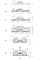
- the solid green laser may be a continuous laser or a pulsed laser.
- the source electrode film and the drain electrode film function as a laser mask. Therefore, only the channel portion of the amorphous silicon film can be selectively annealed by spot irradiation or scanning irradiation of a solid green laser.
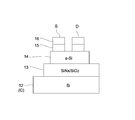
- a gate electrode film 2 is formed on the surface of a substrate 1.
- the gate insulating film 3 is formed of a silicon nitride film (SiNx), a silicon oxide film (SiO 2 ), or the like, and is formed by, for example, a CVD method.
- the thickness of the gate insulating film 3 is, for example, 200 nm to 500 nm.
- an ohmic contact layer 5 and an electrode layer 6 are sequentially laminated on the amorphous silicon film 4.
- a region of the amorphous silicon film 14 (channel portion) located between the source electrode film S and the drain electrode film D is irradiated with a solid green laser, and then a heat treatment (annealing) in a hydrogen atmosphere is performed. 30 minutes at a temperature. It has been confirmed that the heat treatment (annealing) in the hydrogen atmosphere shows a higher mobility improvement effect as the treatment is performed at a higher temperature.
- a preferable heat treatment temperature is 400 ° C. or higher.
- scanning annealing of a solid green laser has been described as an example for laser annealing to the amorphous silicon film 4 (channel portion 41).
- the same effects as described above can also be obtained by spot irradiation.
Abstract
Description
前記絶縁膜は、前記ゲート電極膜上に形成される。前記アモルファスシリコン膜は、前記絶縁膜上に形成される。前記オーミックコンタクト層は、前記アモルファスシリコン膜上に形成され、ソースとドレインに分離される。前記ソース電極膜及び前記ドレイン電極膜は、前記オーミックコンタクト層上に形成される。前記チャネル部は、微結晶構造を有し、前記ソース電極膜及び前記ドレイン電極膜の間に位置する前記アモルファスシリコン膜に固体グリーンレーザを照射して形成される。
前記絶縁膜は、前記ゲート電極膜上に形成される。前記アモルファスシリコン膜は、前記絶縁膜上に形成される。前記オーミックコンタクト層は、前記アモルファスシリコン膜上に形成され、ソースとドレインに分離される。前記ソース電極膜及び前記ドレイン電極膜は、前記オーミックコンタクト層上に形成される。前記チャネル部は、微結晶構造を有し、前記ソース電極膜及び前記ドレイン電極膜の間に位置する前記アモルファスシリコン膜に固体グリーンレーザを照射して形成される。
2、12…ゲート電極膜
3、13…ゲート絶縁膜
4、14…アモルファスシリコン膜
5、15…オーミックコンタクト層
6、16…電極層
71…ソース電極膜
72…ドレイン電極膜
GL…固体グリーンレーザ
Claims (6)
- ゲート電極膜上に絶縁膜を形成し、
前記絶縁膜上にアモルファスシリコン膜を形成し、
前記アモルファスシリコン膜上にソース側とドレイン側に分離されたオーミックコンタクト層と前記オーミックコンタクト層上にソース電極膜及びドレイン電極膜とを形成し、
前記ソース電極膜及び前記ドレイン電極膜をマスクとして前記アモルファスシリコン膜に固体グリーンレーザを照射する
薄膜トランジスタの製造方法。 - 請求項1に記載の薄膜トランジスタの製造方法であって、
前記絶縁膜を形成するステップは、
前記絶縁膜として窒化シリコン膜を形成し、
前記固体グリーンレーザを照射するステップは、
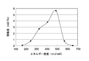
エネルギー密度が100mJ/cm2から700mJ/cm2の前記固体グリーンレーザを照射する
薄膜トランジスタの製造方法。 - 請求項1に記載の薄膜トランジスタの製造方法であって、
前記絶縁膜を形成するステップは、
前記絶縁膜として酸化シリコン膜を形成し、
前記固体グリーンレーザを照射するステップは、
エネルギー密度が100mJ/cm2から700mJ/cm2の前記固体グリーンレーザを照射する
薄膜トランジスタの製造方法。 - 請求項1に記載の薄膜トランジスタの製造方法であって、さらに、
前記絶縁膜上に前記アモルファスシリコン膜を形成した後、前記アモルファスシリコン膜へ前記固体グリーンレーザを照射する前に、前記アモルファスシリコン膜を熱処理する
薄膜トランジスタの製造方法。 - 請求項1に記載の薄膜トランジスタの製造方法であって、さらに、
前記アモルファスシリコン膜へ前記固体グリーンレーザを照射した後、前記アモルファスシリコン膜を水素雰囲気下で熱処理する
薄膜トランジスタの製造方法。 - ゲート電極膜と、
前記ゲート電極膜上に形成された絶縁膜と、
前記絶縁膜上に形成されたアモルファスシリコン膜と、
前記アモルファスシリコン膜上に形成され、ソースとドレインに分離されたオーミックコンタクト層と、
前記オーミックコンタクト層上に形成されたソース電極膜及びドレイン電極膜と、
前記ソース電極膜及び前記ドレイン電極膜の間に位置する前記アモルファスシリコン膜に固体グリーンレーザを照射して形成された微結晶構造のチャネル部と
を具備する薄膜トランジスタ。
Priority Applications (5)
| Application Number | Priority Date | Filing Date | Title |
|---|---|---|---|
| CN2008801227994A CN101939829B (zh) | 2007-12-25 | 2008-12-12 | 薄膜晶体管制造方法以及薄膜晶体管 |
| KR1020107014518A KR101133827B1 (ko) | 2007-12-25 | 2008-12-12 | 박막 트랜지스터의 제조 방법 및 박막 트랜지스터 |
| DE112008003488T DE112008003488B4 (de) | 2007-12-25 | 2008-12-12 | Verfahren zum Herstellen eines Dünnschichttransistors und Dünnschichttransistor |
| JP2009547039A JP4856252B2 (ja) | 2007-12-25 | 2008-12-12 | 薄膜トランジスタの製造方法 |
| US12/808,397 US8673705B2 (en) | 2007-12-25 | 2008-12-12 | Method of producing thin film transistor and thin film transistor |
Applications Claiming Priority (2)
| Application Number | Priority Date | Filing Date | Title |
|---|---|---|---|
| JP2007332774 | 2007-12-25 | ||
| JP2007-332774 | 2007-12-25 |
Publications (1)
| Publication Number | Publication Date |
|---|---|
| WO2009081775A1 true WO2009081775A1 (ja) | 2009-07-02 |
Family
ID=40801081
Family Applications (1)
| Application Number | Title | Priority Date | Filing Date |
|---|---|---|---|
| PCT/JP2008/072685 WO2009081775A1 (ja) | 2007-12-25 | 2008-12-12 | 薄膜トランジスタの製造方法及び薄膜トランジスタ |
Country Status (7)
| Country | Link |
|---|---|
| US (1) | US8673705B2 (ja) |
| JP (1) | JP4856252B2 (ja) |
| KR (1) | KR101133827B1 (ja) |
| CN (1) | CN101939829B (ja) |
| DE (1) | DE112008003488B4 (ja) |
| TW (1) | TW200939357A (ja) |
| WO (1) | WO2009081775A1 (ja) |
Cited By (1)
| Publication number | Priority date | Publication date | Assignee | Title |
|---|---|---|---|---|
| US10818492B2 (en) | 2016-03-16 | 2020-10-27 | V Technology Co., Ltd. | Method for manufacturing thin film transistor and mask for use in the manufacturing method |
Families Citing this family (5)
| Publication number | Priority date | Publication date | Assignee | Title |
|---|---|---|---|---|
| CN103493186A (zh) * | 2011-11-29 | 2014-01-01 | 松下电器产业株式会社 | 薄膜晶体管阵列的制造方法、薄膜晶体管阵列及显示装置 |
| CN109417099A (zh) * | 2016-04-25 | 2019-03-01 | 堺显示器制品株式会社 | 薄膜晶体管、显示装置和薄膜晶体管制造方法 |
| CN108735819B (zh) * | 2017-04-13 | 2020-07-14 | 京东方科技集团股份有限公司 | 低温多晶硅薄膜晶体管及其制造方法、显示基板 |
| KR102622712B1 (ko) * | 2017-10-13 | 2024-01-08 | 더 트러스티이스 오브 콜롬비아 유니버시티 인 더 시티 오브 뉴욕 | 스팟 빔 및 라인 빔 결정화를 위한 시스템들 및 방법들 |
| CN113611752B (zh) * | 2021-07-19 | 2024-01-16 | Tcl华星光电技术有限公司 | 低温多晶硅tft的制作方法及低温多晶硅tft |
Citations (6)
| Publication number | Priority date | Publication date | Assignee | Title |
|---|---|---|---|---|
| JPS60245124A (ja) * | 1984-05-18 | 1985-12-04 | Sony Corp | 半導体装置の製法 |
| JPH0362971A (ja) * | 1989-07-31 | 1991-03-19 | Sanyo Electric Co Ltd | 薄膜トランジスタ |
| JPH04186735A (ja) * | 1990-11-20 | 1992-07-03 | Matsushita Electric Ind Co Ltd | 半導体装置の製造方法 |
| JP2002094078A (ja) * | 2000-06-28 | 2002-03-29 | Semiconductor Energy Lab Co Ltd | 半導体装置 |
| JP2007035964A (ja) * | 2005-07-27 | 2007-02-08 | Sony Corp | 薄膜トランジスタとその製造方法、及び表示装置 |
| JP2007220918A (ja) * | 2006-02-16 | 2007-08-30 | Ulvac Japan Ltd | レーザアニール方法、薄膜半導体装置及びその製造方法、並びに表示装置及びその製造方法 |
Family Cites Families (8)
| Publication number | Priority date | Publication date | Assignee | Title |
|---|---|---|---|---|
| US4459739A (en) * | 1981-05-26 | 1984-07-17 | Northern Telecom Limited | Thin film transistors |
| JP3255942B2 (ja) * | 1991-06-19 | 2002-02-12 | 株式会社半導体エネルギー研究所 | 逆スタガ薄膜トランジスタの作製方法 |
| JPH1056180A (ja) * | 1995-09-29 | 1998-02-24 | Canon Inc | 半導体装置及びその製造方法 |
| TW504846B (en) | 2000-06-28 | 2002-10-01 | Semiconductor Energy Lab | Semiconductor device and manufacturing method thereof |
| JP4030758B2 (ja) * | 2001-12-28 | 2008-01-09 | 株式会社半導体エネルギー研究所 | 半導体装置の作製方法 |
| CN101217150B (zh) * | 2002-03-05 | 2011-04-06 | 株式会社半导体能源研究所 | 半导体元件和使用半导体元件的半导体装置 |
| CN100367479C (zh) * | 2005-02-06 | 2008-02-06 | 友达光电股份有限公司 | 一种薄膜晶体管的制造方法 |
| KR100785020B1 (ko) * | 2006-06-09 | 2007-12-12 | 삼성전자주식회사 | 하부 게이트 박막 트랜지스터 및 그 제조방법 |
-
2008
- 2008-12-12 DE DE112008003488T patent/DE112008003488B4/de active Active
- 2008-12-12 KR KR1020107014518A patent/KR101133827B1/ko active IP Right Grant
- 2008-12-12 US US12/808,397 patent/US8673705B2/en active Active
- 2008-12-12 CN CN2008801227994A patent/CN101939829B/zh active Active
- 2008-12-12 JP JP2009547039A patent/JP4856252B2/ja not_active Expired - Fee Related
- 2008-12-12 WO PCT/JP2008/072685 patent/WO2009081775A1/ja active Application Filing
- 2008-12-23 TW TW097150186A patent/TW200939357A/zh unknown
Patent Citations (6)
| Publication number | Priority date | Publication date | Assignee | Title |
|---|---|---|---|---|
| JPS60245124A (ja) * | 1984-05-18 | 1985-12-04 | Sony Corp | 半導体装置の製法 |
| JPH0362971A (ja) * | 1989-07-31 | 1991-03-19 | Sanyo Electric Co Ltd | 薄膜トランジスタ |
| JPH04186735A (ja) * | 1990-11-20 | 1992-07-03 | Matsushita Electric Ind Co Ltd | 半導体装置の製造方法 |
| JP2002094078A (ja) * | 2000-06-28 | 2002-03-29 | Semiconductor Energy Lab Co Ltd | 半導体装置 |
| JP2007035964A (ja) * | 2005-07-27 | 2007-02-08 | Sony Corp | 薄膜トランジスタとその製造方法、及び表示装置 |
| JP2007220918A (ja) * | 2006-02-16 | 2007-08-30 | Ulvac Japan Ltd | レーザアニール方法、薄膜半導体装置及びその製造方法、並びに表示装置及びその製造方法 |
Cited By (1)
| Publication number | Priority date | Publication date | Assignee | Title |
|---|---|---|---|---|
| US10818492B2 (en) | 2016-03-16 | 2020-10-27 | V Technology Co., Ltd. | Method for manufacturing thin film transistor and mask for use in the manufacturing method |
Also Published As
| Publication number | Publication date |
|---|---|
| CN101939829A (zh) | 2011-01-05 |
| KR20100089895A (ko) | 2010-08-12 |
| JP4856252B2 (ja) | 2012-01-18 |
| US8673705B2 (en) | 2014-03-18 |
| KR101133827B1 (ko) | 2012-04-06 |
| US20100301339A1 (en) | 2010-12-02 |
| TW200939357A (en) | 2009-09-16 |
| DE112008003488B4 (de) | 2012-01-19 |
| CN101939829B (zh) | 2013-03-27 |
| DE112008003488T5 (de) | 2010-10-21 |
| JPWO2009081775A1 (ja) | 2011-05-06 |
Similar Documents
| Publication | Publication Date | Title |
|---|---|---|
| US7323368B2 (en) | Method for manufacturing semiconductor device and heat treatment method | |
| JP3586558B2 (ja) | 薄膜の改質方法及びその実施に使用する装置 | |
| JP4856252B2 (ja) | 薄膜トランジスタの製造方法 | |
| KR101015844B1 (ko) | 박막트랜지스터, 그의 제조방법 및 그를 구비하는유기전계발광표시장치의 제조방법 | |
| JP2007035812A (ja) | 多結晶シリコン膜の製造方法および薄膜トランジスタ | |
| JP2007220918A (ja) | レーザアニール方法、薄膜半導体装置及びその製造方法、並びに表示装置及びその製造方法 | |
| KR20010109211A (ko) | 반도체 장치의 제조 방법 | |
| JPH0794756A (ja) | 半導体装置の作製方法 | |
| JPH06124890A (ja) | 薄膜状半導体装置の作製方法。 | |
| JPH0917729A (ja) | 半導体装置の製造方法 | |
| JP2009147256A (ja) | ディスプレーデバイス用半導体装置の製造方法 | |
| JP2004039660A (ja) | 多結晶半導体膜の製造方法、薄膜トランジスタの製造方法、表示装置、およびパルスレーザアニール装置 | |
| JP3844537B2 (ja) | 多結晶半導体膜の製造方法 | |
| JP4239744B2 (ja) | 薄膜トランジスタの製造方法 | |
| JP2001057432A (ja) | 薄膜素子の転写方法 | |
| JP3925085B2 (ja) | 半導体装置の製造方法、光変調素子の製造方法、および表示装置の製造方法 | |
| JP2000068518A (ja) | 薄膜トランジスタの製造方法 | |
| JP3462157B2 (ja) | 半導体装置の作製方法 | |
| JPH06124889A (ja) | 薄膜状半導体装置の作製方法 | |
| JP2002280304A (ja) | 半導体装置の製造方法 | |
| JPH09237767A (ja) | 半導体装置の製造方法 | |
| WO2010024278A1 (ja) | 薄膜トランジスタの製造方法及び薄膜トランジスタ | |
| JP3393857B2 (ja) | 半導体装置の作製方法 | |
| JP3393863B2 (ja) | 半導体装置の作成方法 | |
| JP3684909B2 (ja) | 薄膜トランジスタ作成方法 |
Legal Events
| Date | Code | Title | Description |
|---|---|---|---|
| WWE | Wipo information: entry into national phase |
Ref document number: 200880122799.4 Country of ref document: CN |
|
| 121 | Ep: the epo has been informed by wipo that ep was designated in this application |
Ref document number: 08864176 Country of ref document: EP Kind code of ref document: A1 |
|
| ENP | Entry into the national phase |
Ref document number: 2009547039 Country of ref document: JP Kind code of ref document: A |
|
| WWE | Wipo information: entry into national phase |
Ref document number: 1120080034885 Country of ref document: DE |
|
| ENP | Entry into the national phase |
Ref document number: 20107014518 Country of ref document: KR Kind code of ref document: A |
|
| WWE | Wipo information: entry into national phase |
Ref document number: 12808397 Country of ref document: US |
|
| RET | De translation (de og part 6b) |
Ref document number: 112008003488 Country of ref document: DE Date of ref document: 20101021 Kind code of ref document: P |
|
| REG | Reference to national code |
Ref country code: DE Ref legal event code: 8607 |
|
| REG | Reference to national code |
Ref country code: DE Ref legal event code: 8607 |
|
| 122 | Ep: pct application non-entry in european phase |
Ref document number: 08864176 Country of ref document: EP Kind code of ref document: A1 |