US9490393B2 - Semiconductor light emitting device with light extraction surface - Google Patents
Semiconductor light emitting device with light extraction surface Download PDFInfo
- Publication number
- US9490393B2 US9490393B2 US12/561,640 US56164009A US9490393B2 US 9490393 B2 US9490393 B2 US 9490393B2 US 56164009 A US56164009 A US 56164009A US 9490393 B2 US9490393 B2 US 9490393B2
- Authority
- US
- United States
- Prior art keywords
- concave
- light emitting
- semiconductor
- emitting device
- slope
- Prior art date
- Legal status (The legal status is an assumption and is not a legal conclusion. Google has not performed a legal analysis and makes no representation as to the accuracy of the status listed.)
- Active, expires
Links
- 239000004065 semiconductor Substances 0.000 title claims abstract description 229
- 238000000605 extraction Methods 0.000 title claims abstract description 79
- 238000002161 passivation Methods 0.000 claims description 24
- 239000011810 insulating material Substances 0.000 claims 1
- 239000000758 substrate Substances 0.000 description 56
- JMASRVWKEDWRBT-UHFFFAOYSA-N Gallium nitride Chemical compound [Ga]#N JMASRVWKEDWRBT-UHFFFAOYSA-N 0.000 description 28
- 238000001465 metallisation Methods 0.000 description 26
- 229910002601 GaN Inorganic materials 0.000 description 24
- 238000009826 distribution Methods 0.000 description 17
- 238000000034 method Methods 0.000 description 17
- 229910052751 metal Inorganic materials 0.000 description 15
- 239000002184 metal Substances 0.000 description 15
- 230000008569 process Effects 0.000 description 13
- VYPSYNLAJGMNEJ-UHFFFAOYSA-N Silicium dioxide Chemical compound O=[Si]=O VYPSYNLAJGMNEJ-UHFFFAOYSA-N 0.000 description 12
- 238000009792 diffusion process Methods 0.000 description 11
- 239000000463 material Substances 0.000 description 9
- 229910052737 gold Inorganic materials 0.000 description 8
- 229910052594 sapphire Inorganic materials 0.000 description 8
- 239000010980 sapphire Substances 0.000 description 8
- 238000004519 manufacturing process Methods 0.000 description 7
- 229910008479 TiSi2 Inorganic materials 0.000 description 6
- DFJQEGUNXWZVAH-UHFFFAOYSA-N bis($l^{2}-silanylidene)titanium Chemical compound [Si]=[Ti]=[Si] DFJQEGUNXWZVAH-UHFFFAOYSA-N 0.000 description 6
- 229910052681 coesite Inorganic materials 0.000 description 6
- 229910052906 cristobalite Inorganic materials 0.000 description 6
- 239000000377 silicon dioxide Substances 0.000 description 6
- 229910052682 stishovite Inorganic materials 0.000 description 6
- 230000003746 surface roughness Effects 0.000 description 6
- WGTYBPLFGIVFAS-UHFFFAOYSA-M tetramethylammonium hydroxide Chemical compound [OH-].C[N+](C)(C)C WGTYBPLFGIVFAS-UHFFFAOYSA-M 0.000 description 6
- 229910052905 tridymite Inorganic materials 0.000 description 6
- 230000000052 comparative effect Effects 0.000 description 5
- 150000001875 compounds Chemical class 0.000 description 5
- 238000005530 etching Methods 0.000 description 5
- 230000008901 benefit Effects 0.000 description 4
- 230000015572 biosynthetic process Effects 0.000 description 4
- 229910052759 nickel Inorganic materials 0.000 description 4
- 230000001902 propagating effect Effects 0.000 description 4
- 238000004544 sputter deposition Methods 0.000 description 4
- 229910052719 titanium Inorganic materials 0.000 description 4
- 229910002704 AlGaN Inorganic materials 0.000 description 3
- 239000012535 impurity Substances 0.000 description 3
- 238000005259 measurement Methods 0.000 description 3
- 150000002739 metals Chemical class 0.000 description 3
- 150000004767 nitrides Chemical class 0.000 description 3
- 230000003287 optical effect Effects 0.000 description 3
- 229910052760 oxygen Inorganic materials 0.000 description 3
- 229910052763 palladium Inorganic materials 0.000 description 3
- 229910052697 platinum Inorganic materials 0.000 description 3
- 229910052710 silicon Inorganic materials 0.000 description 3
- 229910052721 tungsten Inorganic materials 0.000 description 3
- 229910001218 Gallium arsenide Inorganic materials 0.000 description 2
- XUIMIQQOPSSXEZ-UHFFFAOYSA-N Silicon Chemical compound [Si] XUIMIQQOPSSXEZ-UHFFFAOYSA-N 0.000 description 2
- MCMNRKCIXSYSNV-UHFFFAOYSA-N Zirconium dioxide Chemical compound O=[Zr]=O MCMNRKCIXSYSNV-UHFFFAOYSA-N 0.000 description 2
- QVGXLLKOCUKJST-UHFFFAOYSA-N atomic oxygen Chemical compound [O] QVGXLLKOCUKJST-UHFFFAOYSA-N 0.000 description 2
- 230000004888 barrier function Effects 0.000 description 2
- YCIMNLLNPGFGHC-UHFFFAOYSA-N catechol Chemical compound OC1=CC=CC=C1O YCIMNLLNPGFGHC-UHFFFAOYSA-N 0.000 description 2
- 238000005229 chemical vapour deposition Methods 0.000 description 2
- 229910052804 chromium Inorganic materials 0.000 description 2
- 238000005253 cladding Methods 0.000 description 2
- 238000001312 dry etching Methods 0.000 description 2
- 230000000694 effects Effects 0.000 description 2
- 238000010894 electron beam technology Methods 0.000 description 2
- 238000005516 engineering process Methods 0.000 description 2
- 238000010438 heat treatment Methods 0.000 description 2
- 239000012212 insulator Substances 0.000 description 2
- 229910052750 molybdenum Inorganic materials 0.000 description 2
- 239000001301 oxygen Substances 0.000 description 2
- 238000000059 patterning Methods 0.000 description 2
- 238000000206 photolithography Methods 0.000 description 2
- 229920002120 photoresistant polymer Polymers 0.000 description 2
- 238000005268 plasma chemical vapour deposition Methods 0.000 description 2
- 238000001020 plasma etching Methods 0.000 description 2
- 230000009467 reduction Effects 0.000 description 2
- 229910052703 rhodium Inorganic materials 0.000 description 2
- 238000005070 sampling Methods 0.000 description 2
- 239000010703 silicon Substances 0.000 description 2
- 229910052709 silver Inorganic materials 0.000 description 2
- 229910052596 spinel Inorganic materials 0.000 description 2
- 239000000126 substance Substances 0.000 description 2
- XOLBLPGZBRYERU-UHFFFAOYSA-N tin dioxide Chemical compound O=[Sn]=O XOLBLPGZBRYERU-UHFFFAOYSA-N 0.000 description 2
- 229910052720 vanadium Inorganic materials 0.000 description 2
- 238000012935 Averaging Methods 0.000 description 1
- PIICEJLVQHRZGT-UHFFFAOYSA-N Ethylenediamine Chemical compound NCCN PIICEJLVQHRZGT-UHFFFAOYSA-N 0.000 description 1
- 229910005540 GaP Inorganic materials 0.000 description 1
- 229910026161 MgAl2O4 Inorganic materials 0.000 description 1
- 239000012670 alkaline solution Substances 0.000 description 1
- 239000000956 alloy Substances 0.000 description 1
- 229910045601 alloy Inorganic materials 0.000 description 1
- 229910052782 aluminium Inorganic materials 0.000 description 1
- PNEYBMLMFCGWSK-UHFFFAOYSA-N aluminium oxide Inorganic materials [O-2].[O-2].[O-2].[Al+3].[Al+3] PNEYBMLMFCGWSK-UHFFFAOYSA-N 0.000 description 1
- 238000004458 analytical method Methods 0.000 description 1
- 239000012298 atmosphere Substances 0.000 description 1
- 239000000470 constituent Substances 0.000 description 1
- 150000004696 coordination complex Chemical class 0.000 description 1
- 229910052802 copper Inorganic materials 0.000 description 1
- 229910052593 corundum Inorganic materials 0.000 description 1
- 230000000593 degrading effect Effects 0.000 description 1
- 239000007772 electrode material Substances 0.000 description 1
- 239000006023 eutectic alloy Substances 0.000 description 1
- 230000008020 evaporation Effects 0.000 description 1
- 238000001704 evaporation Methods 0.000 description 1
- 229910052732 germanium Inorganic materials 0.000 description 1
- 238000000227 grinding Methods 0.000 description 1
- 229910052735 hafnium Inorganic materials 0.000 description 1
- 230000006872 improvement Effects 0.000 description 1
- 229910052741 iridium Inorganic materials 0.000 description 1
- 229910052742 iron Inorganic materials 0.000 description 1
- 239000007788 liquid Substances 0.000 description 1
- 238000001755 magnetron sputter deposition Methods 0.000 description 1
- 229910052748 manganese Inorganic materials 0.000 description 1
- 239000000203 mixture Substances 0.000 description 1
- 238000012986 modification Methods 0.000 description 1
- 230000004048 modification Effects 0.000 description 1
- 229910003465 moissanite Inorganic materials 0.000 description 1
- 229910052758 niobium Inorganic materials 0.000 description 1
- 239000012299 nitrogen atmosphere Substances 0.000 description 1
- 229910052762 osmium Inorganic materials 0.000 description 1
- 238000005498 polishing Methods 0.000 description 1
- 238000002203 pretreatment Methods 0.000 description 1
- 230000002035 prolonged effect Effects 0.000 description 1
- 229910052707 ruthenium Inorganic materials 0.000 description 1
- 239000000523 sample Substances 0.000 description 1
- SBIBMFFZSBJNJF-UHFFFAOYSA-N selenium;zinc Chemical compound [Se]=[Zn] SBIBMFFZSBJNJF-UHFFFAOYSA-N 0.000 description 1
- 229910010271 silicon carbide Inorganic materials 0.000 description 1
- 238000009751 slip forming Methods 0.000 description 1
- 239000007787 solid Substances 0.000 description 1
- 239000000243 solution Substances 0.000 description 1
- 239000011029 spinel Substances 0.000 description 1
- 229910052715 tantalum Inorganic materials 0.000 description 1
- 230000008685 targeting Effects 0.000 description 1
- 239000012780 transparent material Substances 0.000 description 1
- 238000001039 wet etching Methods 0.000 description 1
- 229910001845 yogo sapphire Inorganic materials 0.000 description 1
- 229910052727 yttrium Inorganic materials 0.000 description 1
- 229910052725 zinc Inorganic materials 0.000 description 1
- 229910052726 zirconium Inorganic materials 0.000 description 1
Images


Classifications
-
- H—ELECTRICITY
- H01—ELECTRIC ELEMENTS
- H01L—SEMICONDUCTOR DEVICES NOT COVERED BY CLASS H10
- H01L33/00—Semiconductor devices with at least one potential-jump barrier or surface barrier specially adapted for light emission; Processes or apparatus specially adapted for the manufacture or treatment thereof or of parts thereof; Details thereof
- H01L33/02—Semiconductor devices with at least one potential-jump barrier or surface barrier specially adapted for light emission; Processes or apparatus specially adapted for the manufacture or treatment thereof or of parts thereof; Details thereof characterised by the semiconductor bodies
- H01L33/20—Semiconductor devices with at least one potential-jump barrier or surface barrier specially adapted for light emission; Processes or apparatus specially adapted for the manufacture or treatment thereof or of parts thereof; Details thereof characterised by the semiconductor bodies with a particular shape, e.g. curved or truncated substrate
- H01L33/22—Roughened surfaces, e.g. at the interface between epitaxial layers
-
- H—ELECTRICITY
- H01—ELECTRIC ELEMENTS
- H01L—SEMICONDUCTOR DEVICES NOT COVERED BY CLASS H10
- H01L33/00—Semiconductor devices with at least one potential-jump barrier or surface barrier specially adapted for light emission; Processes or apparatus specially adapted for the manufacture or treatment thereof or of parts thereof; Details thereof
- H01L33/005—Processes
- H01L33/0062—Processes for devices with an active region comprising only III-V compounds
- H01L33/0066—Processes for devices with an active region comprising only III-V compounds with a substrate not being a III-V compound
- H01L33/007—Processes for devices with an active region comprising only III-V compounds with a substrate not being a III-V compound comprising nitride compounds
-
- H—ELECTRICITY
- H01—ELECTRIC ELEMENTS
- H01L—SEMICONDUCTOR DEVICES NOT COVERED BY CLASS H10
- H01L33/00—Semiconductor devices with at least one potential-jump barrier or surface barrier specially adapted for light emission; Processes or apparatus specially adapted for the manufacture or treatment thereof or of parts thereof; Details thereof
- H01L33/02—Semiconductor devices with at least one potential-jump barrier or surface barrier specially adapted for light emission; Processes or apparatus specially adapted for the manufacture or treatment thereof or of parts thereof; Details thereof characterised by the semiconductor bodies
- H01L33/04—Semiconductor devices with at least one potential-jump barrier or surface barrier specially adapted for light emission; Processes or apparatus specially adapted for the manufacture or treatment thereof or of parts thereof; Details thereof characterised by the semiconductor bodies with a quantum effect structure or superlattice, e.g. tunnel junction
- H01L33/06—Semiconductor devices with at least one potential-jump barrier or surface barrier specially adapted for light emission; Processes or apparatus specially adapted for the manufacture or treatment thereof or of parts thereof; Details thereof characterised by the semiconductor bodies with a quantum effect structure or superlattice, e.g. tunnel junction within the light emitting region, e.g. quantum confinement structure or tunnel barrier
-
- H—ELECTRICITY
- H01—ELECTRIC ELEMENTS
- H01L—SEMICONDUCTOR DEVICES NOT COVERED BY CLASS H10
- H01L33/00—Semiconductor devices with at least one potential-jump barrier or surface barrier specially adapted for light emission; Processes or apparatus specially adapted for the manufacture or treatment thereof or of parts thereof; Details thereof
- H01L33/02—Semiconductor devices with at least one potential-jump barrier or surface barrier specially adapted for light emission; Processes or apparatus specially adapted for the manufacture or treatment thereof or of parts thereof; Details thereof characterised by the semiconductor bodies
- H01L33/14—Semiconductor devices with at least one potential-jump barrier or surface barrier specially adapted for light emission; Processes or apparatus specially adapted for the manufacture or treatment thereof or of parts thereof; Details thereof characterised by the semiconductor bodies with a carrier transport control structure, e.g. highly-doped semiconductor layer or current-blocking structure
- H01L33/145—Semiconductor devices with at least one potential-jump barrier or surface barrier specially adapted for light emission; Processes or apparatus specially adapted for the manufacture or treatment thereof or of parts thereof; Details thereof characterised by the semiconductor bodies with a carrier transport control structure, e.g. highly-doped semiconductor layer or current-blocking structure with a current-blocking structure
-
- H—ELECTRICITY
- H01—ELECTRIC ELEMENTS
- H01L—SEMICONDUCTOR DEVICES NOT COVERED BY CLASS H10
- H01L33/00—Semiconductor devices with at least one potential-jump barrier or surface barrier specially adapted for light emission; Processes or apparatus specially adapted for the manufacture or treatment thereof or of parts thereof; Details thereof
- H01L33/02—Semiconductor devices with at least one potential-jump barrier or surface barrier specially adapted for light emission; Processes or apparatus specially adapted for the manufacture or treatment thereof or of parts thereof; Details thereof characterised by the semiconductor bodies
- H01L33/20—Semiconductor devices with at least one potential-jump barrier or surface barrier specially adapted for light emission; Processes or apparatus specially adapted for the manufacture or treatment thereof or of parts thereof; Details thereof characterised by the semiconductor bodies with a particular shape, e.g. curved or truncated substrate
-
- H—ELECTRICITY
- H01—ELECTRIC ELEMENTS
- H01L—SEMICONDUCTOR DEVICES NOT COVERED BY CLASS H10
- H01L33/00—Semiconductor devices with at least one potential-jump barrier or surface barrier specially adapted for light emission; Processes or apparatus specially adapted for the manufacture or treatment thereof or of parts thereof; Details thereof
- H01L33/02—Semiconductor devices with at least one potential-jump barrier or surface barrier specially adapted for light emission; Processes or apparatus specially adapted for the manufacture or treatment thereof or of parts thereof; Details thereof characterised by the semiconductor bodies
- H01L33/26—Materials of the light emitting region
- H01L33/30—Materials of the light emitting region containing only elements of group III and group V of the periodic system
- H01L33/32—Materials of the light emitting region containing only elements of group III and group V of the periodic system containing nitrogen
-
- H—ELECTRICITY
- H01—ELECTRIC ELEMENTS
- H01L—SEMICONDUCTOR DEVICES NOT COVERED BY CLASS H10
- H01L33/00—Semiconductor devices with at least one potential-jump barrier or surface barrier specially adapted for light emission; Processes or apparatus specially adapted for the manufacture or treatment thereof or of parts thereof; Details thereof
- H01L33/36—Semiconductor devices with at least one potential-jump barrier or surface barrier specially adapted for light emission; Processes or apparatus specially adapted for the manufacture or treatment thereof or of parts thereof; Details thereof characterised by the electrodes
- H01L33/38—Semiconductor devices with at least one potential-jump barrier or surface barrier specially adapted for light emission; Processes or apparatus specially adapted for the manufacture or treatment thereof or of parts thereof; Details thereof characterised by the electrodes with a particular shape
-
- H—ELECTRICITY
- H01—ELECTRIC ELEMENTS
- H01L—SEMICONDUCTOR DEVICES NOT COVERED BY CLASS H10
- H01L33/00—Semiconductor devices with at least one potential-jump barrier or surface barrier specially adapted for light emission; Processes or apparatus specially adapted for the manufacture or treatment thereof or of parts thereof; Details thereof
- H01L33/44—Semiconductor devices with at least one potential-jump barrier or surface barrier specially adapted for light emission; Processes or apparatus specially adapted for the manufacture or treatment thereof or of parts thereof; Details thereof characterised by the coatings, e.g. passivation layer or anti-reflective coating
-
- H—ELECTRICITY
- H01—ELECTRIC ELEMENTS
- H01L—SEMICONDUCTOR DEVICES NOT COVERED BY CLASS H10
- H01L2933/00—Details relating to devices covered by the group H01L33/00 but not provided for in its subgroups
- H01L2933/0083—Periodic patterns for optical field-shaping in or on the semiconductor body or semiconductor body package, e.g. photonic bandgap structures
-
- H01L33/0079—
-
- H—ELECTRICITY
- H01—ELECTRIC ELEMENTS
- H01L—SEMICONDUCTOR DEVICES NOT COVERED BY CLASS H10
- H01L33/00—Semiconductor devices with at least one potential-jump barrier or surface barrier specially adapted for light emission; Processes or apparatus specially adapted for the manufacture or treatment thereof or of parts thereof; Details thereof
- H01L33/005—Processes
- H01L33/0093—Wafer bonding; Removal of the growth substrate
-
- H—ELECTRICITY
- H01—ELECTRIC ELEMENTS
- H01L—SEMICONDUCTOR DEVICES NOT COVERED BY CLASS H10
- H01L33/00—Semiconductor devices with at least one potential-jump barrier or surface barrier specially adapted for light emission; Processes or apparatus specially adapted for the manufacture or treatment thereof or of parts thereof; Details thereof
- H01L33/02—Semiconductor devices with at least one potential-jump barrier or surface barrier specially adapted for light emission; Processes or apparatus specially adapted for the manufacture or treatment thereof or of parts thereof; Details thereof characterised by the semiconductor bodies
- H01L33/20—Semiconductor devices with at least one potential-jump barrier or surface barrier specially adapted for light emission; Processes or apparatus specially adapted for the manufacture or treatment thereof or of parts thereof; Details thereof characterised by the semiconductor bodies with a particular shape, e.g. curved or truncated substrate
- H01L33/24—Semiconductor devices with at least one potential-jump barrier or surface barrier specially adapted for light emission; Processes or apparatus specially adapted for the manufacture or treatment thereof or of parts thereof; Details thereof characterised by the semiconductor bodies with a particular shape, e.g. curved or truncated substrate of the light emitting region, e.g. non-planar junction
-
- H—ELECTRICITY
- H01—ELECTRIC ELEMENTS
- H01L—SEMICONDUCTOR DEVICES NOT COVERED BY CLASS H10
- H01L33/00—Semiconductor devices with at least one potential-jump barrier or surface barrier specially adapted for light emission; Processes or apparatus specially adapted for the manufacture or treatment thereof or of parts thereof; Details thereof
- H01L33/48—Semiconductor devices with at least one potential-jump barrier or surface barrier specially adapted for light emission; Processes or apparatus specially adapted for the manufacture or treatment thereof or of parts thereof; Details thereof characterised by the semiconductor body packages
- H01L33/58—Optical field-shaping elements
Definitions
- the present invention relates to a semiconductor light emitting device, and more particularly relates to a semiconductor light emitting device which is provided with concaves/convexes on a surface for a light extraction (hereinafter, referred to as light extraction surface) for increasing light extraction efficiency.
- a compound semiconductor for example, a gallium nitride (GaN) has been used as a common material for a semiconductor light emitting device such as an LED.
- GaN gallium nitride
- a plurality of concaves/convexes may be formed on a semiconductor layer surface (see paragraph [0050] and FIG. 1 in JP 2000-196152, and paragraphs [0054], [0088], FIG. 1 and FIG. 20 in JP 2007-88277) or a substrate (see paragraph [0042] and FIG. 2 in JP 2003-69075, paragraph [0045] and FIG. 3(b) in JP 2007-67209, and paragraphs [0054], [0088], FIG. 1 and FIG. 20 in JP 2007-88277) for increasing light extraction efficiency of a semiconductor layer which is stacked including a GaN-based light emitting layer in most cases.
- a substrate is composed of a GaN-based compound semiconductor.
- a pit hole, concave
- a plurality of planes appear in a step-like pattern and a slope is formed between the planes.
- a undoped GaN substrate which has a dislocation density not more than 10 6 /cm 2 is used.
- macro concaves/convexes step: 3 ⁇ m are formed by grinding using a grinder on a surface opposite to a surface on which a device made of, for example, GaN-based semiconductor layer is formed, and the ground surface is further chemically treated (dry etching) to form circular cones in high density as micro concaves/convexes (step: not more than 1 ⁇ m).
- the final purpose is to realize a high light emitting efficiency, while targeting a reduction of a driving voltage of the light emitting device as a firsthand purpose by disposing the micro convexes in high density.
- the light emitting device is provided with the macro convexes in a pre-treatment for disposing the micro convexes in high density finally.
- the light emitting device disclosed in JP 2007-88277 is a face-down type device (flip chip).
- Two types of convexes are formed using a pattern either on a surface opposite to a surface on which a GaN-based semiconductor layer is formed on a sapphire substrate or on a surface of n-type semiconductor layer after removal of the sapphire substrate subsequent to a formation of each electrode.
- One is a first convex (1 ⁇ m) which is formed in a long-period and relatively high.
- the other is a second convex (0.3 ⁇ m) which is formed in a short-period and relatively low.
- an interval between convexes is set such that, for example, the long-period is not less than 2.3 ⁇ m and the short-period is not less than 0.46 ⁇ m, based on the experimental data to increase the light extraction efficiency.
- the structure is a concave
- an opening area (surface side portion) of the concave is fixed and the concave has a taper shape in a depth direction from the opening, and if a surface (side surface) of the concave in the depth direction is steeply inclined, a deeper concave may be formed.
- the electrode When the electrode is further stacked as described above, it is necessary to form a depth of the concave relatively shallow by making an inclination of the side surface of the concave gentle. It may be possible to form an opening portion of the concave larger in accordance with a shortened depth of the concave by making the inclination of the side surface of the concave gentle. In this case, however, the concaves/convexes become relatively small, and as a result, the light distribution becomes poor due to approaching to a flat surface.
- the pit as a concave of the light emitting device disclosed in JP 2003-69075, on which an electrode is stacked, is disposed for suppressing an interference to be generated by multiple reflection of light inside the semiconductor device.
- JP 2003-69075 there is no description on what structure of the pit improves the light extraction efficiency.
- a convex is formed on a backside of an undoped GaN substrate for achieving a reduction of a driving voltage, which is a firsthand purpose.
- the convex is not disposed on a light extraction surface of a GaN-based semiconductor layer surface. Therefore, there is no direct relation between a convex structure and light extraction efficiency of a surface on the light extraction side of a semiconductor layer including a light emitting layer.
- the present invention has been developed considering the foregoing problems, and it is an object of the present invention to provide a semiconductor light emitting device which has high light extraction efficiency of a surface on a light extraction side of a semiconductor layer including a light emitting layer and a good light distribution.
- a semiconductor light emitting device which has at least one concave on a light extraction surface opposite to a surface on which a semiconductor stack including a light emitting layer between a n-type semiconductor layer and a p-type semiconductor layer is mounted.
- the concave has not less than two slopes each having a different slope angle in a direction that a diameter of the concave becomes narrower toward a bottom of the concave from an opening of the concave.
- a slope having a gentle slope angle is provided with irregularities and a slope having a steep slope angle is a flat surface.
- the semiconductor light emitting device since the semiconductor light emitting device has a concave on the light extraction surface that is a surface of a semiconductor layer including the light emitting layer, if an electrode (n-electrode or p-electrode) is stacked on the semiconductor layer where the concave is disposed, a current diffusion from the electrode is good (improved) in comparison with a case where a convex is disposed.
- the reason is as follows. When a plurality of convexes are disposed, two adjacent convexes are connected by only a portion of the semiconductor layer below the bottom of the convexes.
- the semiconductor light emitting device since the semiconductor light emitting device has at least two slopes each having a different slope angle in the direction where a diameter of the concave becomes narrower toward the bottom, if a light emitted from the light emitting layer enters a steep slope, the light is output in the upper direction of the concave by refraction, or the light is output in the upper direction of the concave by reflection at another steep slope facing the steep slope after the refraction.
- the semiconductor light emitting device since the semiconductor light emitting device has at least two slopes, a number of reflection can be reduced in comparison with a conventional structure where a number of slope is one and multiple reflection is caused, and as a result, the light is efficiently output in the upper direction.
- the slope having a gentle slope angle is provided with the irregularities and the slope having a steep slope angle is a flat surface in the concave of the semiconductor light emitting device, if a light emitted from the light emitting layer enters and transmits the slope having a gentle slope angle, the transmitted light is scattered. Therefore, even if a light emitted form the light emitting layer obliquely enters the slope having a gentle slope angle, a component of the light propagating in the right upper direction in the total light emitted outside increases. Therefore, the light distribution becomes good, as well as the light extraction efficiency is improved. Furthermore, since a light emitted from the light emitting layer is efficiently reflected when the light enters the slope having a steep slope angle, a light to be emitted outside increases, resulting in improvement of light extraction efficiency.
- the slope of the concave has a gentler slope angle as the slope becomes closer to the opening of the concave.
- the slope of the concave of the semiconductor light emitting device is formed to be gentler as the slope becomes closer to the opening of the concave, a probability that a light once reflected at a slope is continuously reflected many times is reduced in comparison with a reverse case where the slope is formed to be gentler as the slope becomes closer to the bottom of the concave.
- the light emitting device has a slope having a gentler slope angle as the slope becomes closer to the opening of the concave, a light emitted outside is likely to be extracted in the upper direction at a steep angle in comparison with a case where the slope is formed to be gentler as the slope becomes closer to the bottom of the concave.
- the slope angles of the respective slopes of the concave have the relationship described above, the current is easily diffused, and as a result, a uniform light emission can be achieved (obtained) in comparison with a case where the concave is merely disposed.
- the concave has a bottom surface at a bottom and the bottom surface is provided with the irregularities.
- the concave of the semiconductor light emitting device since the concave of the semiconductor light emitting device has a bottom surface, an optical path length of a light which is emitted from the light emitting layer, enters a slope near the bottom of the concave from outside the concave, passes through inside the concave and re-enters a slope facing the foregoing slope becomes long in comparison with a case where the concave has no bottom surface. If the concave has no bottom surface, a light which is emitted from the semiconductor layer and enters a slope near the bottom of the concave from outside the concave passes through the concave in a short time and re-enters an adjacent semiconductor layer from a slope facing the foregoing slope.
- the light receives more effect of refraction inside the concave by the prolonged optical path length due to the existence of the bottom surface, and a reflected light at a slope facing the foregoing slope may enter another different slope close to the opening of the concave. Namely, re-entering of a light emitted from a semiconductor layer into the semiconductor layer can be reduced.
- a plurality of the concaves are disposed on the light extraction surface, adjacent openings of the plurality of the concaves are separated each other, and a separating area which separates the adjacent openings is provided with the irregularities.
- an electrode is disposed on the light extraction surface.
- a current diffusion from the electrode in the semiconductor light emitting device becomes good in comparison with a case where a convex is disposed.
- the electrode is disposed in an area other than the concave on the light extraction surface.
- a shape of the opening of the concave may be formed in a circle in plan view of the light extraction surface.
- the slope of the concave can be easily tapered.
- a shape of the opening of the concave is a polygon in plan view of the light extraction surface.
- openings of adjacent concaves in plan view can be arranged in contact with each other by a point or line in high density.
- a shape of the opening of the concave is a hexagon in plan view of the light extraction surface.
- respective centers of the plurality of concaves 90 are in line in each row and in line every other column, and the plurality of concaves whose openings are in contact with each other by a tangent line or a point can be close-packed. Namely, many concaves can be effectively and integrally arranged in a small surface area.
- a depth of the concave has a length not less than half of a thickness between the light extraction surface and the light emitting layer and less than the thickness between the light extraction surface and the light emitting layer.
- the slope of the concave is close to the light emitting layer, the light can be efficiently extracted outside from the semiconductor layer.
- the slope of the concave is covered with a passivation film.
- the passivation film is formed by a material having a refractive index between those of the semiconductor layer on the slope side and an outside material on the opposite side of the slope so that the light is easily extracted.
- the passivation film is formed by SiO 2 or Al 2 O 3 .
- the concave is disposed in the n-type semiconductor layer.
- the concave can be formed deeper.
- a relatively deep concave can be formed in the total thickness of the semiconductor light emitting layer.
- a light can be efficiently extracted outside from the semiconductor layer.
- the n-electrode stacked on the n-type semiconductor layer is small in size in comparison with the p-electrode, when a plurality of n-electrodes are dispersively arranged, the n-electrodes can be easily arranged so that a current uniformly diffuses in the semiconductor layer.
- the concave is disposed at a position facing a p-electrode which is disposed on the surface on which the semiconductor stack is mounted.
- a light emitted from the light emitting layer toward a surface opposite to the light extraction surface is reflected at the p-electrode, and the reflection light is easily extracted outside the semiconductor layer from the concave.
- a plurality of n-electrodes can be dispersively arranged in consideration of a current diffusion to be determined depending on the arrangement of the p-electrode. For example, when a plurality of n-electrodes are disposed on an area other than the concave, the p-electrode and the n-electrode are arranged so that the p-electrode does not face the n-electrode in the depth direction of the semiconductor stack.
- a current easily diffuses, especially, in the semiconductor layer.
- a current is likely to flow along a path connecting the p-electrode and the n-electrode, and the current does not uniformly flow as seen in the horizontal direction, resulting in generation of uneven current distribution.
- a semiconductor light emitting device which can easily extract a light outside from a surface on a light extraction side that is a surface of a semiconductor layer including a light emitting layer, and has a good light distribution.
- an electrode is stacked on a semiconductor layer on which the concave is disposed, a current easily and uniformly diffuses in the semiconductor layer. Since the current easily and uniformly diffuses in the semiconductor layer, it is unnecessary that a semiconductor layer, where the concave just beneath the stacked electrode is disposed, has an excessive thickness.
- a depth of the concave can be made shallower in comparison with the conventional one. In this case, the light extraction efficiency can be further improved, accordingly.
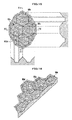
- FIG. 1 is a cross sectional view schematically showing a structure of a semiconductor light emitting device according to an embodiment of the present invention
- FIG. 2 is a cross sectional view schematically showing an enlarged concave shown in FIG. 1 ;
- FIG. 3 is a view schematically showing a plane, X-X cross section and Y-Y cross section of a concave;
- FIG. 4 is a perspective view schematically showing a partial cross section of a concave shown in FIG. 3 ;
- FIG. 5A to FIG. 5D are cross sectional views schematically showing a comparison between a concave of a semiconductor light emitting device according to the present embodiment and concaves other than the present embodiment, where FIG. 5A shows the concave according to the present embodiment and FIG. 5B to FIG. 5D show comparative examples;
- FIG. 6 is a graph showing a relationship between a roughness of a light extraction surface and a light directionality
- FIG. 7 is a graph showing an example of a light directionality of a semiconductor light emitting device according to the embodiment.
- FIG. 8A to FIG. 8F are cross sectional views schematically showing fabrication processes of the semiconductor light emitting device shown in FIG. 1 (first);
- FIG. 9A to FIG. 9E are cross sectional views schematically showing fabrication processes of the semiconductor light emitting device shown in FIG. 1 (second);
- FIG. 10 is a flowchart showing formation processes of the concave shown in FIG. 9C ;
- FIG. 11 is a view schematically showing a cross section in a depth direction of a first modified example of a concave structure
- FIG. 12 is a view schematically showing a cross section in a depth direction of a second modified example of a concave structure
- FIG. 13 is a view schematically showing a plane, X-X cross section and Y-Y cross section of a first modified example of an opening of a concave;
- FIG. 14 is a perspective view schematically showing a partial cross section of the concave shown in FIG. 13 ;
- FIG. 15 is a view schematically showing a plane, X-X cross section and Y-Y cross section of a second modified example of an opening of a concave;
- FIG. 16 is a perspective view schematically showing a partial cross section of the concave shown in FIG. 15 ;
- FIG. 17 is a view schematically showing a plane, X-X cross section and Y-Y cross section of a third modified example of an opening of a concave.
- FIG. 18 is a perspective view schematically showing a partial cross section of the concave shown in FIG. 17 .
- a light emitting device relates to the light emitting device where at least one concave is disposed on a light extraction surface opposite to a surface on which a substrate of a semiconductor stack having a light emitting layer between a n-type semiconductor layer and a p-type semiconductor layer is mounted.
- FIG. 1 is a cross sectional view schematically showing a structure of a semiconductor light emitting device according to an embodiment of the present invention
- FIG. 2 is a cross sectional view schematically showing an enlarged concave shown in FIG. 1
- FIG. 3 is a view schematically showing a plane, X-X cross section and Y-Y cross section of a concave
- FIG. 4 is a perspective view schematically showing a partial cross section of the concave shown in FIG. 3 .
- a semiconductor light emitting device 1 mainly consists of a substrate 10 , a metallization layer 20 , a p-electrode 30 , a passivation film 40 , a semiconductor stack 50 , an n-electrode 60 , a passivation film 70 and a backside metallization layer 80 .
- the Substrate 10 is Made of Silicon (Si). Meanwhile, other than Si, for example, a semiconductor substrate made of a semiconductor such as Ge, SiC, GaN, GaAs, GaP, InP, ZnSe, ZnS and ZnO, or a single metal substrate, or a metal substrate made of metal complex which is composed of not less than two metals which are mutually immiscible or have a small solid solubility limit may be used. As a single metal substrate, specifically, a Cu substrate can be used.
- a metal substrate specifically, a substrate which is composed of at least one metal selected from a highly-conductive metal such as Ag, Cu, Au and Pt and at least one metal selected from a high hardness metal such as W, Mo, Cr and Ni may be used.
- a device for example, a zener diode may be added to the substrate 10 .
- a complex of Cu—W or Cu—Mo may be preferably used.
- a metallization layer 20 is a eutectic alloy for bonding two substrates in a fabrication process of the semiconductor light emitting device 1 . Specifically, a metallization layer 21 on the epitaxial side shown in FIG. 8D and a metallization layer 22 on the substrate side shown in FIG. 8E are bonded to form the metallization layer 20 .
- the metallization layer 21 on the epitaxial side is formed by stacking, for example, Ti/Pt/Au/Sn/Au in this order from the bottom in FIG. 8D .
- the metallization layer 22 on the substrate side is formed by stacking, for example, Au/Pt/TiSi 2 , or TiSi 2 /Pt/Pd in this order from the top in FIG. 8E .
- a p-electrode 30 is formed on a mounting surface of a semiconductor stack 50 on the side of substrate 10 and at positions facing the concaves 90 on the uppermost surface of the semiconductor stack 50 in the depth direction.
- the p-electrode 30 consists of at least two layers, a p-electrode first layer (not shown) on the side of semiconductor stack 50 and a p-electrode second layer (not shown) on the lower side of the p-electrode first layer.
- the following materials are commonly used for the p-electrode first layer (not shown).
- a metal and alloy of Ag, Zn, Ni, Pt, Pd, Rh, Ru, Os, Ir, Ti, Zr, Hf, V, Nb, Ta, Co, Fe, Mn, Mo, Cr, W, La, Cu and Y, and a single film or stacked film of, for example, conductive oxides such as ITO, ZnO and SnO 2 may be used.
- Pt, Au and Ni—Ti—Au based electrode material may be used.
- the p-electrode 30 consists of a two-layer structure of p-electrode first layer/p-electrode second layer, a stacked layer structure of, for example, Pt/Au, Pd/Au, Rh/Au and Ni/Au may be used. If the p-electrode 30 consists of a three-layer structure by inserting a p-electrode third layer between the p-electrode first layer and the p-electrode second layer, a stacked layer structure of, for example, Ni/Pt/Au, Pd/Pt/Au and Rh/Pt/Au may be used.
- the p-electrode 30 consists of a four-layer structure by inserting a p-electrode third layer and p-electrode fourth layer between the p-electrode first layer and the p-electrode second layer, a stacked layer structure of, for example, Ag/Ni/Ti/Pt may be used.
- a passivation film 40 is made of a transparent material which has a refractive index lower than that of a p-type semiconductor layer 53 and formed on a plane identical to that of the p-electrode 30 at portions where the p-electrode 30 is not formed and.
- the passivation film 40 is made of an insulator film, preferably made of an oxide film.
- the passivation film 40 is made of, for example, SiO 2 or ZrO 2 .
- the passivation film 40 may be formed by a well known method, such as sputtering, ECR (Electron Cyclotron Resonance) sputtering, CVD (Chemical Vapor Deposition), ECR-CVD, ECR-plasma CVD, evaporation and EB (Electron Beam).
- the passivation film 40 is preferably formed by, for example, ECR sputtering, ECR-CVD and ECR-plasma CVD.
- a semiconductor stack 50 is made of, for example, GaN-based compound semiconductor (for example, GaN, AlGaN, InGaN and AlGaInN). Especially, GaN is preferable because an etched surface of GaN has a fine crystalline surface.
- the semiconductor stack 50 is formed by sequentially stacking an n-type semiconductor layer 51 , a light emitting layer 52 and a p-type semiconductor layer 53 in this order from the side of a light extraction surface opposite to a surface to be mounted on the substrate 10 . Meanwhile, the semiconductor stack 50 is generally expressed by In x Al y Ga 1-x-y N (0 ⁇ x ⁇ 1, 0 ⁇ y ⁇ 1, 0 ⁇ x+y ⁇ 1).
- the light extraction surface is a surface of the n-type semiconductor layer 51 . That is, the concave 90 is disposed on the n-type semiconductor layer 51 .
- the concave 90 will be described later in detail.
- the n-type semiconductor layer 51 is made of GaN containing, for example, Si, Ge and O (oxygen) as an n-type impurity.
- the n-type semiconductor layer 51 may be formed by a plurality of layers.
- the light emitting layer 52 is made of, for example, InGaN.
- the p-type semiconductor layer 53 is made of, for example, GaN containing Mg as a p-type impurity.
- the light extraction surface of the semiconductor stack 50 On the light extraction surface of the semiconductor stack 50 , at least one electrode is formed.
- the light extraction surface is formed on a surface of the n-type semiconductor layer 51 . Therefore, the electrode formed on the extraction surface is the n-electrode 60 .
- the n-electrode 60 is formed on an area other than the concave 90 on the light extraction surface.
- the light extraction surface is a surface of the n-type semiconductor layer 51
- the n-electrode 60 is electrically connected to the area other than the concave 90 on the upper surface of the n-type semiconductor layer 51 .
- the n-electrode is connected to the outside by a bonding wire.
- the n-electrode 60 consists of a metal stack, for example, Ti/Pt/Au, Ti/Pt/Au/Ni, Ti/Al, Ti/Al/Pt/Au, W/Pt/Au and V/Pt/Au, which are formed by stacking the metals in this order on the upper side of the n-type semiconductor layer 51 . Meanwhile, the n-electrode 60 may be composed of an ohmic contact and pad electrode.
- a passivation film 70 is formed by a material identical to that of the above-mentioned passivation film 40 . Namely, for example, if the passivation film 40 is made of SiO 2 , the passivation film 70 is also made of SiO 2 , and compositions of the both films may be slightly different each other depending on a forming method thereof.
- the passivation film 70 covers an upper surface of the n-electrode 60 except a wire bonding area, an inside of the concave 90 including the inner circumferential surface, a surface of the n-type semiconductor layer 51 and a side face of the semiconductor stack 50 .
- a backside metallization layer 80 is formed on a surface of the substrate 10 opposite to a surface on which a metallization layer 20 is formed, and functions as an ohmic electrode.
- the backside metallization layer 80 is made of a metal stack, for example, TiSi 2 /Pt/Au, which is formed by sequentially stacking the metals in this order from the upper side in FIG. 1 .
- the concave 90 has, as shown in FIG. 2 , two slopes 93 , 94 each having a different slope angle in a direction that a diameter of the concave 90 becomes narrower toward a bottom surface 92 from an opening 91 .
- the slope angle is formed to become gentler as a position of the slope is closer to the opening 91 of the concave 90 .
- the concave 90 becomes narrower as a position leaves from a surface of the n-type semiconductor layer 51 , and a side surface of the concave 90 has the two slopes 93 , 94 having respective different narrowing angles ⁇ 1 , ⁇ 2 .
- FIG. 2 corresponds to a cross section taken along X-X line of FIG. 3 .
- a slope (slope 93 ) having a gentler slope angle close to the opening 91 is a surface having irregularities 95
- the slope 94 having a steeper slope angle has a flat surface.
- the irregularities 95 identical to that of the slope 93 are also formed on a bottom of the concave 90 .
- a plurality of the concaves 90 are disposed on the light extraction surface, adjacent openings of the plurality of the concaves 90 are separated from each other, and a separating area 201 is also provided with the irregularities 95 .
- An average surface roughness (Ra) corresponding to a size of the irregularities 95 formed on the slope 93 is 10 to 100 nm, preferably 15 to 60 nm, and most preferably 20 to 40 nm. Meanwhile, a depth of the concave 90 is defined as described later, and it is, for example, several micrometers ( ⁇ m). Therefore, the irregularities 95 formed on the slope 93 are called micro irregularities.
- the average surface roughness (Ra) in the present invention may be measured using a scanning probe microscope (SPI3800N manufactured by SII).
- the average surface roughness (Ra) can be measured from a cross section of a surface to be measured (hereinafter, referred to as measurement surface) based on a definition of arithmetical mean roughness Ra of JIS B0601.
- an average line (wave line) is acquired from a profiling curve of the measurement surface, and the average line is subtracted from the profiling curve. That is, by replacing the average line with a straight line, a roughness curve is acquired.
- a direction identical to the average line which is replaced with a straight line is set to an X-axis and a direction orthogonal to the X-axis and parallel to the cross section is set to a Z-axis.
- an average line of the sampling portion can be expressed by the following formula (1).
- the average surface roughness (Ra) is a value which is acquired by averaging absolute values of deviations (differences) between Z(x) and Z 0 , and can be acquired by the following formula (2).
- Ra 1 l ⁇ ⁇ 0 l ⁇ ⁇ Z ⁇ ( x ) - Z 0 ⁇ ⁇ ⁇ d x formula ⁇ ⁇ ( 2 )
- a measurement surface is observed at a cross section described above using a microscope which is capable of high magnification such as, for example, TEM, and an average line and a roughness curve are acquired from the profiling curve.
- An arbitrary 500 nm span is selected on the X-axis, in the selected span, a hundred X-values (X 1 to X 100 ) are set at constant intervals, and a Z-value (Z(X 1 ) to Z(X 100 )) at each X-value is measured.
- Z 0 can be acquired from the measured Z-value using formula (3).
- Z 0 (1/100) ⁇ Z ( x 1 )+ Z ( x 2 )+ Z ( x 3 )+ . . . + Z ( x 100 ) ⁇ formula (3)
- Ra (1/100) ⁇
- the narrowing angles ⁇ 1 , ⁇ 2 are defined as an angle which is formed by the horizontal plane of the semiconductor stack 50 and the respective slopes 93 , 94 .
- the narrowing angle ⁇ 1 on the surface side is larger than 0° and less than 60°, preferably 20 to 50°.
- the narrowing angle ⁇ 2 on the side of the light emitting layer 52 is larger than 60° and less than 90°, preferably 60 to 80°.
- a difference between the narrowing angles ⁇ 1 , ⁇ 2 is considerably large, a light emitted from the light emitting layer 52 at various angles can be easily extracted by efficiently reflecting and transmitting the light by the slopes 93 , 94 . For example, as shown in FIG.
- each of the slopes 93 , 94 is preferably made of GaN. Further, it is more preferable if a concentration of n-type impurity (for example, Si) doped into the GaN of each of the slopes 93 , 94 is varied. In addition, it may be possible that the slope 93 on the surface side is made of undoped GaN and the slope 94 on the side of the light emitting layer 52 is made of si-doped GaN.
- a depth D of the concave 90 has a length not less than half of a thickness H that is a distance from the light extraction surface to the light emitting layer 52 and less than the thickness H(H/2 ⁇ D ⁇ H).
- a depth D 1 corresponding to the slope 93 is deeper than a depth D 2 corresponding to the slope 94 for easy forming of the concave 90 .
- a bottom size W (diameter W) of the concave 90 is not less than 1 ⁇ 5 and not more than 1 ⁇ 2 of an opening size L (maximum width L) of the opening 91 (L/5 ⁇ W ⁇ L/2), while depending on the narrowing angles ⁇ 1 , ⁇ 2 , and preferably not less than 1 ⁇ 3 and not more than 1 ⁇ 2 (L/3 ⁇ W ⁇ L/2).
- a difference between the bottom size W of the concave 90 and the opening size L of the opening 91 is considerably large, a light emitted from the light emitting layer 52 at various angles can be easily extracted by efficiently reflecting and transmitting the light by the slopes 93 , 94 .
- the bottom size W of the concave 90 is set to 1 ⁇ 3 of the opening size L of the opening 91 , since the depth D 1 corresponding to the slope 93 in the depth D of the concave 90 can be set deeper than the depth D 2 corresponding to the slope 94 , while setting the narrowing angles ⁇ 1 , ⁇ 2 in the foregoing ranges, a formation of the concave 90 becomes easy. Because of the above-mentioned reason, the narrowing angles ⁇ 1 , ⁇ 2 are set in the foregoing ranges.
- each opening of the concaves 90 a to 90 g is surrounded by an area 201 of the light extraction surface. Therefore, a current diffusion on the light extraction surface is good. It is noted that the area 201 may be a flat surface or a curved surface.
- the micro irregularities 95 are shown by fine dots in the plane view of FIG. 3 and in FIG. 4 . Then, only an area of the steep slope 94 in the concave 90 is shown with white (without fine dots). This is the same with any other drawings such as FIG. 13 . It is noted that the micro irregularities 95 are overdrawn for convenience for explanation as shown in FIG. 2 .
- FIG. 5A to FIG. 5D are cross sectional views schematically showing a comparison between a concave of a semiconductor light emitting device according to the embodiment and concaves other than the embodiment.
- FIG. 5A shows an example (example of embodiment) of a cross section of the concave 90 in the semiconductor light emitting device 1 according to the embodiment
- FIG. 5B to FIG. 5D show cross sections of concaves each having a different structure.
- a COMPARATIVE EXAMPLE 1 shown in FIG. 5B is a shallow concave 190 A with a slope having only a gentle slope angle.
- the shallow concave 190 A if a light emitted from a light emitting layer in a semiconductor layer obliquely enters the slope, the light transmits in an oblique direction depending on a difference of a refractive index between an inside and outside substances of the slope, and as a result, the light does not propagate in the right upper direction. Namely, both the light extraction efficiency and light distribution become poor.
- a COMPARATIVE EXAMPLE 2 shown in FIG. 5C is a deep concave 190 B with a slope having only a steep slope angle. If a light emitted from a light emitting layer in a semiconductor layer enters the slope from inside the deep concave 190 B, the light is extracted outside after repeating a reflection at the slope. However, if an electrode is disposed on the light extraction surface of the deep concave 190 B, a current diffusion from the electrode becomes poor.
- the concave 90 that is an example of the embodiment shown in FIG. 5A has two slopes 93 , 94 each having a different slope angle.
- the slope 93 having a gentle slope angle is a surface which is provided with the irregularities 95 and the slope 94 having a steep slope angle is a flat surface. Therefore, in the concave 90 , if a light emitted from a light emitting layer in a semiconductor layer obliquely enters the slope 93 having a gentle slope angle and micro irregularities 95 , the light is scattered by the micro irregularities 95 , and as a result, a component of the light propagating in the right upper direction increases.
- the micro irregularities 95 are also disposed on the bottom surface 92 and the area 201 , when a light emitted from a light emitting layer in a semiconductor layer enters the bottom surface 92 and the area 201 , the light is scattered by the micro irregularities 95 . Therefore, the light extraction efficiency and light distribution become good in comparison with a flat surface without the micro irregularities 95 .
- a COMPARATIVE EXAMPLE 3 shown in FIG. 5D is a fictitious concave 190 C, where in the two slopes each having a different slope angle, a slope 193 having a gentle slope angle is a flat surface and a slope 194 having a steep slope angle is a surface provided with the irregularities 95 .
- a slope 193 having a gentle slope angle is a flat surface
- a slope 194 having a steep slope angle is a surface provided with the irregularities 95 .
- FIG. 6 is a graph showing a relationship between a roughness of a light extraction surface and a light directionality.
- FIG. 6 shows a light directionality with a polar coordinate, and a radial direction indicates a light intensity and a circumferential direction shows an angle.
- a negative direction of the horizontal axis (X-axis) indicates 0° (zero degree) directivity angle
- a positive direction of the horizontal axis (X-axis) indicates 180° directivity angle with reference to 90° (vertical axis: Y-axis) directivity angle.
- a dotted line indicates a case where the light extraction surface is flat and a solid line indicates a case where the light extraction surface is provided with concaves/convexes.
- an absolute value at 90° directivity angle is normalized to “1” for making clear the difference between the both light distributions.
- the light intensity is largest at 90° directivity angle.
- the light extraction surface is flat (dotted line in FIG. 6 )
- the light intensity is largest at 50° and 130° directivity angles, which is 1.8 times larger than the light intensity at 90° directivity angle. Namely, if the light extraction surface is provided with concaves/convexes, the light distribution is improved in comparison with a flat surface.
- FIG. 7 is a graph showing an example of a light directionality of a semiconductor light emitting device according to the embodiment.
- FIG. 7 is drawn with the same scheme as FIG. 6 .
- a solid line indicates data of the semiconductor light emitting device 1 according to the embodiment, that is, the data in a case where the semiconductor light emitting device 1 is provided with the micro irregularities 95 like the concave 90 .
- a dotted line indicates data in a case where the semiconductor light emitting device 1 is not provided with the micro irregularities 95 .
- FIG. 7 it is known that an existence of micro irregularities effects on a light intensity at around 90° directivity angle. Namely, if the micro irregularities 95 are disposed on a concave, a light intensity increases at around 90° directivity angle, and the light distribution is improved.
- FIG. 8A to FIG. 8F and FIG. 9A to FIG. 9E are cross sectional views schematically showing a fabrication process of the semiconductor light emitting device shown in FIG. 1 .
- a n-type semiconductor layer 51 , a light emitting layer 52 and a p-type semiconductor layer 53 are grown in this order on a substrate 100 for growing semiconductor layers (hereinafter, referred to as semiconductor growing substrate 100 ) to form a semiconductor stack 50 .
- the semiconductor growing substrate 100 is a substrate which is removed in a later process and made of a sapphire having one of a C-plane, R-plane and A-plane as a main plane. Meanwhile, a substrate different from sapphire may be used as the semiconductor growing substrate 100 .
- an insulator substrate such as spinel (MgAl 2 O 4 ), SiC (including 6H, 4H and 3C), ZnS, ZnO, GaAs and an oxide substrate whose lattice matches with those of nitride semiconductors may be used as the semiconductor growing substrate 100 , which are materials on which nitride semiconductors can be grown and well known as a substrate material.
- a passivation film 40 is formed between the p-electrodes 30 , 30 using ECR sputtering.
- a metallization layer 21 on an epitaxial layer side is grown on the p-electrode and the passivation film 40 .
- a metallization layer 22 on a substrate side is grown on the substrate 10 as shown in FIG. 8E .
- the metallization layer 22 on the substrate side and the metallization layer 21 on the epitaxial side are bonded by turning back the substrate 10 on which the metallization layer 22 on the substrate side is grown.
- a metallization layer 20 is formed by the bonded metallization layers 21 and 22 on the epitaxial layer side and on the substrate side, respectively.
- the semiconductor growing substrate 100 is removed from the semiconductor stack 50 .
- an upper surface (surface of n-type semiconductor layer 51 ) of the semiconductor stack 50 which is an uppermost surface due to turning back of the substrate 10 from which the semiconductor growing substrate 100 is removed, is polished by CMP (Chemical Mechanical Polishing).
- CMP Chemical Mechanical Polishing
- the concave 90 is formed on the upper surface (surface of n-type semiconductor layer 51 ) of the semiconductor stack 50 by a process described later.
- the n-electrode 60 is formed on an area where the concave 90 is not formed on the upper surface (surface of n-type semiconductor layer 51 ) of the semiconductor stack 50 .
- an inside of the concave 90 including a circumferential surface and the upper surface (surface of n-type semiconductor layer 51 ) of the semiconductor stack 50 are covered with a passivation film 70 .
- a side face of the semiconductor stack 50 is also covered with the passivation film 70 .
- a backside metallization layer 80 as an ohmic electrode is formed on the surface of the substrate 10 , which became an uppermost surface (bottommost surface in FIG. 1 ) by turning back the substrate 10 (not shown), then, the wafer is diced.
- the wafer is divided into bars, a mirror is formed on an end face of a resonator, the bars are cleaved into chips and wires are bonded to the n-electrode 60 and a surface of the backside metallization layer 80 to fabricate the semiconductor light emitting device 1 shown in FIG. 1 .
- FIG. 10 is a flowchart showing a forming process of a concave shown in FIG. 9C .
- a resist pattern having an opened area corresponding to the concave 90 is formed on an upper surface (surface of n-type semiconductor layer 51 ) of the semiconductor stack 50 by, for example, photolithography (step S 1 ).
- a post-bake heat treatment
- step S 2 a post-bake (heat treatment) is conducted at, for example, 180° C. so that an end portion of the resist pattern is deformed to incline by the heat treatment of the resist pattern, as well as abridge formation of the resist is promoted.
- a post-bake heat treatment
- a structure where the end portion of the resist pattern is collapsed to incline from the periphery toward the area to become the concave 90 is formed. Namely, an inclined portion formed by the collapse of the pattern end portion is formed just inside from a periphery of the etching area. As a result, an area having a low etching rate in comparison with no resist area is formed.
- an area to become the concave 90 is dry-etched by, for example, RIE (Reactive Ion Etching) using the resist mask (step S 3 ). Since the area having a low etching rate is formed on the upper surface (surface of n-type semiconductor layer 51 ) of the semiconductor stack 50 , the surface is etched so that there are two inclined stages.
- RIE Reactive Ion Etching
- step S 4 the resist pattern used for the etching as a mask is stripped (step S 4 ).
- a well known common method is used for stripping the resist pattern.
- a photoresist stripping liquid may be used, or an apparatus which irradiates the photoresist with, for example, oxygen plasma (asking) such as an asher may be used.
- an entire wafer surface is wet-etched without patterning.
- an etchant of wet-etching for example, KOH solution, TMAH (tetramethyl ammonium hydroxide) alkaline solution and EPD (ethylene diamine pyrocatechol) may be used.
- KOH solution KOH solution
- TMAH tetramethyl ammonium hydroxide
- EPD ethylene diamine pyrocatechol
- the micro irregularities 95 are formed on an area other than the slope 94 having a steep slope angle. Namely, the micro irregularities 95 are formed on the slope 93 having a gentle slope angle, the bottom surface 92 and the area 201 on the light extraction surface. It is noted that the micro irregularities 95 are formed beneath the n-electrode 60 (see FIG. 1 and FIG. 9E )
- the concave 90 is disposed on the light extraction surface that is the upper surface of the semiconductor stack 50 , it becomes easy to efficiently extract a light outside from a surface on the light extraction side in comparison with a case where a convex is disposed instead of the concave 90 .
- the concave 90 since the slope 93 having a gentle slope angle is provided with the micro irregularities 95 and the slope 94 having a steep slope angle has a flat surface, the light directionality becomes good. Furthermore, a current diffusion from the n-electrode 60 becomes good due to existence of the concave 90 .
- the semiconductor light emitting device 1 since the two slopes 93 , 94 each having a different slope angle in the direction that a diameter of the concave 90 becomes narrower toward the bottom surface 92 from the opening 91 are formed to have a gentler angle as the slopes 93 , 94 become closer to the opening 91 of the concave 90 , a light emitted from the light emitting layer 92 is easily extracted outside by reflection.
- the concave 90 since the concave 90 has the bottom surface 92 , a re-entering of a light, which is emitted from the semiconductor stack 50 (semiconductor layer), into the semiconductor stack 50 can be reduced.
- the present invention has been explained. However, the present invention is not limited to the embodiment described above and can be embodied in various forms without departing from the spirits of the invention.
- the light extraction surface of the semiconductor stack 50 was the n-type semiconductor layer 51 .
- the light extraction surface may be the p-type semiconductor layer 53 and the concave 90 may be disposed on the p-type semiconductor layer 53 .
- the concave 90 is disposed like the embodiment since the concave 90 can be formed deeper.
- the two slopes 93 , 94 were disposed in the concave 90 .
- a concave which has not less than three slopes has the same advantages as long as a narrowing angle (slope angle) of a slope is formed to be gentler as the slope becomes closer to the opening 91 of the concave 90 .
- a narrowing angle corresponding to at least one slope to be disposed between the slopes 93 , 94 is set between ⁇ 1 and ⁇ 2 as appropriate so that a difference among the narrowing angles becomes as equal as possible, while the narrowing angle ⁇ 1 corresponding to the slope on the surface side and the narrowing angle ⁇ 2 corresponding to the slope on the light emitting layer 52 are set in the above-mentioned ranges.
- the n-electrode 60 is disposed in an area without the concave 90 .
- the n-electrode 60 may be disposed on the concave 90 .
- the n-electrode 60 is preferably disposed like the embodiment because a current in the semiconductor stack 50 (semiconductor layer) is easily diffused.
- a material composing the semiconductor stack 50 of the semiconductor light emitting device 1 is not limited to nitride semiconductors.
- the bottom surface 92 of the concave 90 was flat. However, it is not always necessary that the bottom surface is flat, but the bottom surface, for example, may be a curved surface protruding downward. In addition, in the present invention, the bottom surface 92 is not always necessary on a bottom of the concave 90 , but the slope 94 may be narrowed in a reverse circular cone toward the bottom.
- a slope angle of each of the slopes 93 , 94 of the concave 90 is formed to be gentler as the slope is closer to the opening 91 of the concave 90 .
- the present invention is not limited to this.
- a slope 93 B having a steep slope angle and a slope 94 B having a gentle slope angle may be formed in this order from the opening.
- a slope having a gentle slope angle is provided with the irregularities 95 and a slope having a steep slope angle has a flat surface as the foregoing embodiment. Therefore, as shown in FIG. 12 , the micro irregularities 95 are continuously formed from the slope 94 B to the bottom surface 92 .
- a semiconductor light emitting device having such a structure as the concave 90 B also has good light extraction efficiency and good light distribution.
- FIG. 13 is a view schematically showing a plane, X-X cross section and Y-Y cross section of a first modified example of an opening of a concave
- FIG. 14 is a perspective view schematically showing a partial cross section of the first modified example taken along Y-Y cross section shown in FIG. 13
- a configuration of the opening is the same as that of concave 90 shown in FIG. 3 except that a shape of a plurality of concave openings is a hexagon and that a density of the concave opening is not so high as shown in FIG. 3 .
- each vertex of the regular hexagon as an opening is in contact with six concaves 90 b to 90 g surrounding the concave 90 a .
- the concave 90 a is surrounded by six regular triangles shown in plane view of FIG. 13 . These six triangles are located on the light extraction surface. Therefore, a current diffusion on the light extraction surface becomes good.
- each vertex of the regular hexagon as an opening may be separated by a predetermined distance from the six surrounding concaves.
- FIG. 15 is a view schematically showing a plane, X-X cross section and Y-Y cross section of a second modified example of an opening of a concave
- FIG. 16 is a perspective view schematically showing a partial cross section of the second modified example taken along Y-Y cross section shown in FIG. 15 .
- an arrangement of openings of a plurality of concaves is shown in FIG. 15 , which is a close-packed structure.
- the concave 90 a is in contact with six surrounding concaves by respective sides of a regular hexagon as an opening.
- the concave 90 a is in contact with six surrounding concaves at respective vertexes of the regular hexagon as an opening.
- FIG. 15 is a view schematically showing a plane, X-X cross section and Y-Y cross section of a second modified example of an opening of a concave
- FIG. 16 is a perspective view schematically showing a partial cross section of the second modified example taken along Y-Y cross section shown in FIG.
- each side of the regular hexagon as an opening of the concave 90 a is straight and on the light extraction surface.
- each side and each vertex of the opening of the concave are in contact with adjacent concaves by forming a close-packed structure.
- many concaves can be efficiently arranged and integrated in a small surface.
- FIG. 17 is a view schematically showing a plane, X-X cross section and Y-Y cross section of a third modified example of an opening of a concave
- FIG. 18 is a perspective view schematically showing a partial cross section of the third modified example taken along Y-Y cross section of FIG. 17
- each side of a regular hexagon as an opening of the concave 90 a is not a straight line, but a v-shaped line having a vertex (bottom) at the center of the side. Namely, only respective vertexes of the regular hexagon in plane view are located on a plane identical to the light extraction surface.
- an upper slope (slope 93 see FIG.
- V-shape is located below a valley of the V-shape.
- the V-shape is within the upper slope (slope 93 , see FIG. 2 ). Therefore, there is an advantage that a current can be easily and uniformly diffused in comparison with a case where the v-shape is not formed.
- Other characteristics are the same with those of the second modified example and the explanation will be omitted.
- a circle and hexagon in plane view as a shape of the opening 91 of the concave 90 have been exemplified.
- a polygon and ellipsoid such as a triangle and quadrangle can be surely used.
- a circle or hexagon which is capable of forming a close-packed structure is preferable for efficiently diffusing a current and improving the light extraction efficiency.
- a semiconductor light emitting device according to the embodiment of the present invention was fabricated for confirming advantages of the present invention. Specifically, a semiconductor light emitting device 1 was fabricated according to the fabrication processes shown in FIG. 8A to FIG. 10 .
- a sapphire substrate was used for the substrate 100 for growing semiconductor layers (semiconductor growing substrate 100 ).
- a silicon (Si) wafer substrate 400 ⁇ m thick was used as a substrate 10 .
- the following layers were grown on the sapphire substrate for forming the semiconductor stack 50 .
- a n-type cladding layer composed of Si-doped AlGaN and a n-type light guiding layer composed of GaN were grown on the sapphire substrate.
- the n-type semiconductor layer 51 , 4000 nm thick was formed.
- a barrier layer composed of Si-doped In 0.05 Ga 0.95 N and a well layer composed of undoped In 0.1 Ga 0.9 N were alternately grown two times, and further another barrier layer was grown thereon to form a multiple-quantum well (MQW) structure that is the light emitting layer 52 .
- MQW multiple-quantum well
- the wafer was annealed at 700° C. in nitrogen atmosphere for further lowering a resistance of the p-type semiconductor layer 53 .
- the p-electrode 30 , 400 nm thick has a layer structure of Ag/Ni/Ti/Pt in this order from the semiconductor stack 50 .
- the passivation film 40 , 400 nm thick was made of SiO 2 .
- the metallization layer 21 on the epitaxial layer side has a thickness of 1400 nm, and Ti/Pt/Au/Sn/Au were grown in this order from the bottom in FIG. 8D .
- the metallization layer 22 on the substrate side has a thickness of 653 nm, and Au/Pt/TiSi 2 or TiSi 2 /Pt/Pd were grown in this order.
- a depth D of the concave 90 formed on the n-type semiconductor layer 51 using, for example, photolithography and dry-etching was 2500 nm.
- the micro irregularities 95 having a surface roughness of 30 nm were formed by immersing the wafer into TMAH.
- the n-electrode 60 , 1300 nm thick has a layer structure of Ti/Pt/Au in this order from the upper side of the n-type semiconductor layer 51 .
- the passivation layer 70 , 400 nm thick was made of SiO 2 .
- the backside metallization layer 80 has a thickness of 753 nm, and TiSi 2 /Pt/Au were grown in this order on the substrate 10 .
- the semiconductor light emitting device 1 configured as described above shows the light distribution indicated with solid line in FIG. 7 .
- a semiconductor light emitting device can be utilized in various fields, for example, lighting, exposure, display, various kinds of analysis and optical network.
Priority Applications (1)
| Application Number | Priority Date | Filing Date | Title |
|---|---|---|---|
| US15/216,402 US10381516B2 (en) | 2008-09-19 | 2016-07-21 | Semiconductor light emitting device having a recess with irregularities |
Applications Claiming Priority (2)
| Application Number | Priority Date | Filing Date | Title |
|---|---|---|---|
| JP2008241798A JP5282503B2 (ja) | 2008-09-19 | 2008-09-19 | 半導体発光素子 |
| JP2008-241798 | 2008-09-19 |
Related Child Applications (1)
| Application Number | Title | Priority Date | Filing Date |
|---|---|---|---|
| US15/216,402 Continuation US10381516B2 (en) | 2008-09-19 | 2016-07-21 | Semiconductor light emitting device having a recess with irregularities |
Publications (2)
| Publication Number | Publication Date |
|---|---|
| US20100072501A1 US20100072501A1 (en) | 2010-03-25 |
| US9490393B2 true US9490393B2 (en) | 2016-11-08 |
Family
ID=42036730
Family Applications (2)
| Application Number | Title | Priority Date | Filing Date |
|---|---|---|---|
| US12/561,640 Active 2031-02-20 US9490393B2 (en) | 2008-09-19 | 2009-09-17 | Semiconductor light emitting device with light extraction surface |
| US15/216,402 Active US10381516B2 (en) | 2008-09-19 | 2016-07-21 | Semiconductor light emitting device having a recess with irregularities |
Family Applications After (1)
| Application Number | Title | Priority Date | Filing Date |
|---|---|---|---|
| US15/216,402 Active US10381516B2 (en) | 2008-09-19 | 2016-07-21 | Semiconductor light emitting device having a recess with irregularities |
Country Status (2)
| Country | Link |
|---|---|
| US (2) | US9490393B2 (ja) |
| JP (1) | JP5282503B2 (ja) |
Cited By (1)
| Publication number | Priority date | Publication date | Assignee | Title |
|---|---|---|---|---|
| US11393958B2 (en) * | 2016-03-30 | 2022-07-19 | Sony Corporation | Light emitting device to improve the extraction efficiency |
Families Citing this family (44)
| Publication number | Priority date | Publication date | Assignee | Title |
|---|---|---|---|---|
| EP2660883B1 (en) | 2009-12-09 | 2019-03-27 | LG Innotek Co., Ltd. | Light emitting device, light emitting device manufacturing method, light emitting package, and lighting system |
| KR100999779B1 (ko) * | 2010-02-01 | 2010-12-08 | 엘지이노텍 주식회사 | 발광소자, 발광소자의 제조방법 및 발광소자 패키지 |
| JP5052636B2 (ja) * | 2010-03-11 | 2012-10-17 | 株式会社東芝 | 半導体発光素子 |
| EP2555222B1 (en) | 2010-03-29 | 2016-04-06 | Japan Science and Technology Agency | Electron microscope |
| EP2387081B1 (en) * | 2010-05-11 | 2015-09-30 | Samsung Electronics Co., Ltd. | Semiconductor light emitting device and method for fabricating the same |
| KR101761385B1 (ko) | 2010-07-12 | 2017-08-04 | 엘지이노텍 주식회사 | 발광 소자 |
| JP5687858B2 (ja) * | 2010-07-30 | 2015-03-25 | スタンレー電気株式会社 | 半導体発光装置 |
| US8502244B2 (en) * | 2010-08-31 | 2013-08-06 | Micron Technology, Inc. | Solid state lighting devices with current routing and associated methods of manufacturing |
| JP5204177B2 (ja) * | 2010-09-06 | 2013-06-05 | 株式会社東芝 | 半導体発光素子及びその製造方法 |
| KR101707118B1 (ko) * | 2010-10-19 | 2017-02-15 | 엘지이노텍 주식회사 | 발광소자 및 그 발광 소자의 제조 방법 |
| JP5862354B2 (ja) * | 2011-04-15 | 2016-02-16 | 三菱化学株式会社 | 窒化物系発光ダイオード素子とその製造方法 |
| KR101861997B1 (ko) * | 2011-10-31 | 2018-05-29 | 엘지이노텍 주식회사 | 발광소자 및 발광소자 제조방법 |
| US9847372B2 (en) * | 2011-12-01 | 2017-12-19 | Micron Technology, Inc. | Solid state transducer devices with separately controlled regions, and associated systems and methods |
| US8685774B2 (en) * | 2011-12-27 | 2014-04-01 | Sharp Laboratories Of America, Inc. | Method for fabricating three-dimensional gallium nitride structures with planar surfaces |
| JP5292456B2 (ja) * | 2011-12-28 | 2013-09-18 | Dowaエレクトロニクス株式会社 | Iii族窒化物半導体素子およびその製造方法 |
| JP5509394B2 (ja) | 2012-02-01 | 2014-06-04 | パナソニック株式会社 | 半導体発光素子、その製造方法及び光源装置 |
| KR102022659B1 (ko) * | 2012-02-20 | 2019-11-04 | 서울바이오시스 주식회사 | 고효율 발광 다이오드 및 그것을 제조하는 방법 |
| EP2942820A1 (en) | 2012-04-02 | 2015-11-11 | Asahi Kasei E-materials Corporation | Optical substrate, semiconductor light-emitting element and method of manufacturing semiconductor light-emitting element |
| US9276164B2 (en) * | 2012-11-26 | 2016-03-01 | Epistar Corporation | Optoelectronic device and method for manufacturing the same |
| US9559259B2 (en) | 2012-12-31 | 2017-01-31 | Epistar Corporation | Light-emitting device and manufacturing method thereof |
| JP6198416B2 (ja) * | 2013-03-08 | 2017-09-20 | スタンレー電気株式会社 | 半導体発光素子及びその製造方法 |
| JP6256220B2 (ja) * | 2013-06-17 | 2018-01-10 | 王子ホールディングス株式会社 | 半導体発光素子用基板、半導体発光素子、半導体発光素子用基板の製造方法、および、半導体発光素子の製造方法 |
| EP2955762B1 (en) | 2013-07-17 | 2017-09-13 | Marubun Corporation | Semiconductor light-emitting element and production method thereof |
| WO2015016246A1 (ja) * | 2013-07-30 | 2015-02-05 | Dowaエレクトロニクス株式会社 | 半導体発光素子の製造方法、および半導体発光素子 |
| JP6136717B2 (ja) * | 2013-07-31 | 2017-05-31 | 日亜化学工業株式会社 | 発光素子、発光装置及び発光素子の製造方法 |
| US20170012244A1 (en) * | 2014-02-10 | 2017-01-12 | Panasonic Intellectual Property Management Co., Ltd. | Organic electroluminescent element and illumination device |
| CN105934833B (zh) | 2014-03-06 | 2017-09-15 | 丸文株式会社 | 深紫外led及其制造方法 |
| JP6527695B2 (ja) * | 2014-12-22 | 2019-06-05 | スタンレー電気株式会社 | 半導体発光装置 |
| KR101848034B1 (ko) | 2015-01-16 | 2018-04-11 | 마루분 가부시키가이샤 | 심자외 led 및 그 제조 방법 |
| JP6676308B2 (ja) * | 2015-08-07 | 2020-04-08 | ローム株式会社 | 半導体装置 |
| JP6582738B2 (ja) * | 2015-08-26 | 2019-10-02 | 日亜化学工業株式会社 | 発光素子及び発光装置 |
| WO2017038961A1 (ja) | 2015-09-03 | 2017-03-09 | 丸文株式会社 | 深紫外led及びその製造方法 |
| JP6668863B2 (ja) * | 2016-03-22 | 2020-03-18 | 日亜化学工業株式会社 | 発光素子 |
| KR101811819B1 (ko) | 2016-03-30 | 2017-12-22 | 마루분 가부시키가이샤 | 심자외 led 및 그 제조 방법 |
| JP6871706B2 (ja) * | 2016-09-30 | 2021-05-12 | 日機装株式会社 | 半導体発光素子の製造方法 |
| KR101781305B1 (ko) * | 2016-10-18 | 2017-09-25 | 엘지이노텍 주식회사 | 발광 소자, 발광 소자 패키지 및 조명 시스템 |
| FR3059828B1 (fr) * | 2016-12-02 | 2019-05-31 | Commissariat A L'energie Atomique Et Aux Energies Alternatives | Dispositif optoelectronique a diode electroluminescente a extraction augmentee |
| JP6719424B2 (ja) * | 2017-06-26 | 2020-07-08 | 日機装株式会社 | 半導体発光素子および半導体発光素子の製造方法 |
| JP6863835B2 (ja) | 2017-06-26 | 2021-04-21 | 日機装株式会社 | 半導体発光素子および半導体発光素子の製造方法 |
| TWI705585B (zh) * | 2017-09-25 | 2020-09-21 | 致伸科技股份有限公司 | 光源模組 |
| TWI666792B (zh) * | 2017-09-27 | 2019-07-21 | 致伸科技股份有限公司 | 光源模組以及光源模組之製造方法 |
| TWI804567B (zh) | 2018-01-26 | 2023-06-11 | 日商丸文股份有限公司 | 深紫外led及其製造方法 |
| KR102468815B1 (ko) * | 2018-04-04 | 2022-11-18 | 쑤저우 레킨 세미컨덕터 컴퍼니 리미티드 | 반도체 소자 |
| US20230411562A1 (en) * | 2022-06-21 | 2023-12-21 | Creeled, Inc. | Light extraction structures for light-emitting diode chips and related methods |
Citations (20)
| Publication number | Priority date | Publication date | Assignee | Title |
|---|---|---|---|---|
| US20020123164A1 (en) * | 2001-02-01 | 2002-09-05 | Slater David B. | Light emitting diodes including modifications for light extraction and manufacturing methods therefor |
| US6495862B1 (en) | 1998-12-24 | 2002-12-17 | Kabushiki Kaisha Toshiba | Nitride semiconductor LED with embossed lead-out surface |
| JP2003069075A (ja) | 2001-08-28 | 2003-03-07 | Nichia Chem Ind Ltd | 窒化ガリウム系化合物半導体素子 |
| US6657236B1 (en) * | 1999-12-03 | 2003-12-02 | Cree Lighting Company | Enhanced light extraction in LEDs through the use of internal and external optical elements |
| US20050179130A1 (en) * | 2003-08-19 | 2005-08-18 | Hisanori Tanaka | Semiconductor device |
| JP2005268809A (ja) | 2004-03-19 | 2005-09-29 | Lumileds Lighting Us Llc | 面内発光層を含む半導体発光素子 |
| US20050212002A1 (en) * | 2004-03-29 | 2005-09-29 | Daisuke Sanga | Semiconductor light emitting device |
| JP2006013500A (ja) | 2004-06-24 | 2006-01-12 | Shogen Koden Kofun Yugenkoshi | 発光装置 |
| US20060097271A1 (en) * | 2002-07-31 | 2006-05-11 | Osram Opto Semiconductors Gmbh | Gan-based radiation-emitting thin-layered semiconductor component |
| US20060204865A1 (en) * | 2005-03-08 | 2006-09-14 | Luminus Devices, Inc. | Patterned light-emitting devices |
| US20070018187A1 (en) | 2005-07-22 | 2007-01-25 | Samsung Electro-Mechanics Co., Ltd. | Vertical GaN-based LED and method of manfacturing the same |
| JP2007059418A (ja) | 2005-08-22 | 2007-03-08 | Showa Denko Kk | 窒化ガリウム系化合物半導体発光素子 |
| JP2007067209A (ja) | 2005-08-31 | 2007-03-15 | Sanyo Electric Co Ltd | 窒化物系半導体発光素子及びその製造方法 |
| JP2007088277A (ja) | 2005-09-22 | 2007-04-05 | Matsushita Electric Works Ltd | 半導体発光素子およびその製造方法 |
| JP2007184313A (ja) | 2005-12-29 | 2007-07-19 | Rohm Co Ltd | 半導体発光素子およびその製法 |
| US20070264733A1 (en) | 2006-05-10 | 2007-11-15 | Samsung Electro-Mechanics Co., Ltd. | Method of manufacturing vertical gallium nitride-based light emitting diode |
| US20080035953A1 (en) | 2006-08-14 | 2008-02-14 | Samsung Electro-Mechanics Co., Ltd. | Gallium nitride-based light emitting diode and method of manufacturing the same |
| US20080067916A1 (en) * | 2006-07-28 | 2008-03-20 | Epistar Corporation | Light emitting device having a patterned substrate and the method thereof |
| US20080128731A1 (en) * | 2006-11-15 | 2008-06-05 | The Regents Of The University Of California | Transparent mirrorless light emitting diode |
| US20090159908A1 (en) * | 2007-12-19 | 2009-06-25 | Philips Lumileds Lighting Company Llc | Semiconductor light emitting device with light extraction structures |
Family Cites Families (9)
| Publication number | Priority date | Publication date | Assignee | Title |
|---|---|---|---|---|
| US6277665B1 (en) * | 2000-01-10 | 2001-08-21 | United Epitaxy Company, Ltd. | Fabrication process of semiconductor light-emitting device with enhanced external quantum efficiency |
| JP2003078162A (ja) * | 2001-08-31 | 2003-03-14 | Shin Etsu Handotai Co Ltd | GaP系半導体発光素子 |
| US6995032B2 (en) * | 2002-07-19 | 2006-02-07 | Cree, Inc. | Trench cut light emitting diodes and methods of fabricating same |
| JP4168866B2 (ja) * | 2003-07-25 | 2008-10-22 | トヨタ自動車株式会社 | 車両情報通信方法、車両情報通信システムおよびセンター |
| US7791061B2 (en) * | 2004-05-18 | 2010-09-07 | Cree, Inc. | External extraction light emitting diode based upon crystallographic faceted surfaces |
| US7534633B2 (en) * | 2004-07-02 | 2009-05-19 | Cree, Inc. | LED with substrate modifications for enhanced light extraction and method of making same |
| US7256483B2 (en) * | 2004-10-28 | 2007-08-14 | Philips Lumileds Lighting Company, Llc | Package-integrated thin film LED |
| US7481415B2 (en) * | 2006-07-07 | 2009-01-27 | Stanford Mu Corporation | Multi-force actuator valve with multiple operating modes |
| JP4835377B2 (ja) * | 2006-10-20 | 2011-12-14 | 日立電線株式会社 | 半導体発光素子 |
-
2008
- 2008-09-19 JP JP2008241798A patent/JP5282503B2/ja active Active
-
2009
- 2009-09-17 US US12/561,640 patent/US9490393B2/en active Active
-
2016
- 2016-07-21 US US15/216,402 patent/US10381516B2/en active Active
Patent Citations (22)
| Publication number | Priority date | Publication date | Assignee | Title |
|---|---|---|---|---|
| US6495862B1 (en) | 1998-12-24 | 2002-12-17 | Kabushiki Kaisha Toshiba | Nitride semiconductor LED with embossed lead-out surface |
| US6657236B1 (en) * | 1999-12-03 | 2003-12-02 | Cree Lighting Company | Enhanced light extraction in LEDs through the use of internal and external optical elements |
| JP2007019560A (ja) | 2001-02-01 | 2007-01-25 | Cree Inc | 光抽出用の改良を含む発光ダイオード及びその製造方法 |
| US20040217362A1 (en) * | 2001-02-01 | 2004-11-04 | Slater David B | Light emitting diodes including pedestals |
| US20020123164A1 (en) * | 2001-02-01 | 2002-09-05 | Slater David B. | Light emitting diodes including modifications for light extraction and manufacturing methods therefor |
| JP2003069075A (ja) | 2001-08-28 | 2003-03-07 | Nichia Chem Ind Ltd | 窒化ガリウム系化合物半導体素子 |
| US20060097271A1 (en) * | 2002-07-31 | 2006-05-11 | Osram Opto Semiconductors Gmbh | Gan-based radiation-emitting thin-layered semiconductor component |
| US20050179130A1 (en) * | 2003-08-19 | 2005-08-18 | Hisanori Tanaka | Semiconductor device |
| JP2005268809A (ja) | 2004-03-19 | 2005-09-29 | Lumileds Lighting Us Llc | 面内発光層を含む半導体発光素子 |
| US20050212002A1 (en) * | 2004-03-29 | 2005-09-29 | Daisuke Sanga | Semiconductor light emitting device |
| JP2006013500A (ja) | 2004-06-24 | 2006-01-12 | Shogen Koden Kofun Yugenkoshi | 発光装置 |
| US20060204865A1 (en) * | 2005-03-08 | 2006-09-14 | Luminus Devices, Inc. | Patterned light-emitting devices |
| US20070018187A1 (en) | 2005-07-22 | 2007-01-25 | Samsung Electro-Mechanics Co., Ltd. | Vertical GaN-based LED and method of manfacturing the same |
| JP2007059418A (ja) | 2005-08-22 | 2007-03-08 | Showa Denko Kk | 窒化ガリウム系化合物半導体発光素子 |
| JP2007067209A (ja) | 2005-08-31 | 2007-03-15 | Sanyo Electric Co Ltd | 窒化物系半導体発光素子及びその製造方法 |
| JP2007088277A (ja) | 2005-09-22 | 2007-04-05 | Matsushita Electric Works Ltd | 半導体発光素子およびその製造方法 |
| JP2007184313A (ja) | 2005-12-29 | 2007-07-19 | Rohm Co Ltd | 半導体発光素子およびその製法 |
| US20070264733A1 (en) | 2006-05-10 | 2007-11-15 | Samsung Electro-Mechanics Co., Ltd. | Method of manufacturing vertical gallium nitride-based light emitting diode |
| US20080067916A1 (en) * | 2006-07-28 | 2008-03-20 | Epistar Corporation | Light emitting device having a patterned substrate and the method thereof |
| US20080035953A1 (en) | 2006-08-14 | 2008-02-14 | Samsung Electro-Mechanics Co., Ltd. | Gallium nitride-based light emitting diode and method of manufacturing the same |
| US20080128731A1 (en) * | 2006-11-15 | 2008-06-05 | The Regents Of The University Of California | Transparent mirrorless light emitting diode |
| US20090159908A1 (en) * | 2007-12-19 | 2009-06-25 | Philips Lumileds Lighting Company Llc | Semiconductor light emitting device with light extraction structures |
Non-Patent Citations (1)
| Title |
|---|
| Japanese Office Action application No. 2008-241798 dated Dec. 18, 2012. |
Cited By (1)
| Publication number | Priority date | Publication date | Assignee | Title |
|---|---|---|---|---|
| US11393958B2 (en) * | 2016-03-30 | 2022-07-19 | Sony Corporation | Light emitting device to improve the extraction efficiency |
Also Published As
| Publication number | Publication date |
|---|---|
| JP2010074008A (ja) | 2010-04-02 |
| JP5282503B2 (ja) | 2013-09-04 |
| US20160329465A1 (en) | 2016-11-10 |
| US10381516B2 (en) | 2019-08-13 |
| US20100072501A1 (en) | 2010-03-25 |
Similar Documents
| Publication | Publication Date | Title |
|---|---|---|
| US10381516B2 (en) | Semiconductor light emitting device having a recess with irregularities | |
| US8883529B2 (en) | Method for manufacturing semiconductor light emitting device | |
| US10297720B2 (en) | Light emitting diode and method of manufacturing the same | |
| US10224455B2 (en) | Light emitting device and method of forming the same | |
| US6657237B2 (en) | GaN based group III-V nitride semiconductor light-emitting diode and method for fabricating the same | |
| JP5493252B2 (ja) | 半導体発光素子 | |
| JP4932283B2 (ja) | 窒化物半導体発光素子及びその製造方法 | |
| TWI317177B (en) | Semiconductor light emitting device and semiconductor light emitting apparatus | |
| US7683385B2 (en) | Facet extraction LED and method for manufacturing the same | |
| US20200020828A1 (en) | Semiconductor light-emitting device and method of manufacturing the same | |
| US20110303938A1 (en) | Group III nitride semiconductor light-emitting element | |
| US10177278B2 (en) | Semiconductor light emitting device | |
| JP2011061036A (ja) | Iii族窒化物半導体発光素子 | |
| JP2007150259A (ja) | 窒化物半導体発光素子およびその製造方法 | |
| US20160211417A1 (en) | Semiconductor light-emitting element, light emitting device, and method of manufacturing semiconductor light-emitting element | |
| KR20140065105A (ko) | 고효율 발광 다이오드 | |
| CN113497406B (zh) | 半导体激光二极管的制造方法和半导体激光二极管 | |
| US8441023B2 (en) | Semiconductor light emitting device | |
| KR101060975B1 (ko) | 에어갭을 구비하는 발광소자 및 그 제조방법 | |
| JP2004111493A (ja) | 窒化物半導体発光素子とその製造方法 | |
| KR20060134490A (ko) | 플립 칩 질화물반도체 발광 다이오드 및 그의 제조 방법 | |
| EP4356438A1 (en) | Micro light-emitting diode with improved light extraction | |
| KR20100061134A (ko) | 질화물 반도체 발광소자의 제조방법 및 이 방법에 의해 제조된 질화물 반도체 발광소자 | |
| JP2008182037A (ja) | 発光素子およびその製造方法 | |
| KR20140143657A (ko) | 고효율 발광 소자 및 그 제조 방법 |
Legal Events
| Date | Code | Title | Description |
|---|---|---|---|
| AS | Assignment |
Owner name: NICHIA CORPORATION,JAPAN Free format text: ASSIGNMENT OF ASSIGNORS INTEREST;ASSIGNORS:WAKAI, YOHEI;ONISHI, MASAHIKO;REEL/FRAME:023250/0349 Effective date: 20090826 Owner name: NICHIA CORPORATION, JAPAN Free format text: ASSIGNMENT OF ASSIGNORS INTEREST;ASSIGNORS:WAKAI, YOHEI;ONISHI, MASAHIKO;REEL/FRAME:023250/0349 Effective date: 20090826 |
|
| STCF | Information on status: patent grant |
Free format text: PATENTED CASE |
|
| MAFP | Maintenance fee payment |
Free format text: PAYMENT OF MAINTENANCE FEE, 4TH YEAR, LARGE ENTITY (ORIGINAL EVENT CODE: M1551); ENTITY STATUS OF PATENT OWNER: LARGE ENTITY Year of fee payment: 4 |
|
| MAFP | Maintenance fee payment |
Free format text: PAYMENT OF MAINTENANCE FEE, 8TH YEAR, LARGE ENTITY (ORIGINAL EVENT CODE: M1552); ENTITY STATUS OF PATENT OWNER: LARGE ENTITY Year of fee payment: 8 |