US9320107B2 - Vehicular lamp - Google Patents
Vehicular lamp Download PDFInfo
- Publication number
- US9320107B2 US9320107B2 US14/559,049 US201414559049A US9320107B2 US 9320107 B2 US9320107 B2 US 9320107B2 US 201414559049 A US201414559049 A US 201414559049A US 9320107 B2 US9320107 B2 US 9320107B2
- Authority
- US
- United States
- Prior art keywords
- bypass
- state
- control
- units
- driving current
- Prior art date
- Legal status (The legal status is an assumption and is not a legal conclusion. Google has not performed a legal analysis and makes no representation as to the accuracy of the status listed.)
- Active
Links
- 230000005856 abnormality Effects 0.000 claims abstract description 181
- 230000002159 abnormal effect Effects 0.000 claims abstract description 74
- 238000012545 processing Methods 0.000 claims description 33
- 238000012544 monitoring process Methods 0.000 claims description 12
- 230000015572 biosynthetic process Effects 0.000 abstract description 11
- 238000001514 detection method Methods 0.000 description 24
- 230000004313 glare Effects 0.000 description 6
- 230000000977 initiatory effect Effects 0.000 description 5
- 238000010586 diagram Methods 0.000 description 3
- 239000004065 semiconductor Substances 0.000 description 3
- 238000007599 discharging Methods 0.000 description 2
- 238000005516 engineering process Methods 0.000 description 2
- 238000000034 method Methods 0.000 description 2
- 238000009751 slip forming Methods 0.000 description 2
- 230000007423 decrease Effects 0.000 description 1
- 230000000694 effects Effects 0.000 description 1
- 229910044991 metal oxide Inorganic materials 0.000 description 1
- 150000004706 metal oxides Chemical class 0.000 description 1
- 238000012986 modification Methods 0.000 description 1
- 230000004048 modification Effects 0.000 description 1
- 230000002093 peripheral effect Effects 0.000 description 1
- 230000006641 stabilisation Effects 0.000 description 1
- 238000011105 stabilization Methods 0.000 description 1
Images


Classifications
-
- H05B33/089—
-
- H—ELECTRICITY
- H05—ELECTRIC TECHNIQUES NOT OTHERWISE PROVIDED FOR
- H05B—ELECTRIC HEATING; ELECTRIC LIGHT SOURCES NOT OTHERWISE PROVIDED FOR; CIRCUIT ARRANGEMENTS FOR ELECTRIC LIGHT SOURCES, IN GENERAL
- H05B47/00—Circuit arrangements for operating light sources in general, i.e. where the type of light source is not relevant
- H05B47/10—Controlling the light source
- H05B47/105—Controlling the light source in response to determined parameters
-
- B—PERFORMING OPERATIONS; TRANSPORTING
- B60—VEHICLES IN GENERAL
- B60Q—ARRANGEMENT OF SIGNALLING OR LIGHTING DEVICES, THE MOUNTING OR SUPPORTING THEREOF OR CIRCUITS THEREFOR, FOR VEHICLES IN GENERAL
- B60Q11/00—Arrangement of monitoring devices for devices provided for in groups B60Q1/00 - B60Q9/00
-
- H05B33/083—
-
- H—ELECTRICITY
- H05—ELECTRIC TECHNIQUES NOT OTHERWISE PROVIDED FOR
- H05B—ELECTRIC HEATING; ELECTRIC LIGHT SOURCES NOT OTHERWISE PROVIDED FOR; CIRCUIT ARRANGEMENTS FOR ELECTRIC LIGHT SOURCES, IN GENERAL
- H05B45/00—Circuit arrangements for operating light-emitting diodes [LED]
- H05B45/40—Details of LED load circuits
- H05B45/44—Details of LED load circuits with an active control inside an LED matrix
- H05B45/48—Details of LED load circuits with an active control inside an LED matrix having LEDs organised in strings and incorporating parallel shunting devices
-
- H—ELECTRICITY
- H05—ELECTRIC TECHNIQUES NOT OTHERWISE PROVIDED FOR
- H05B—ELECTRIC HEATING; ELECTRIC LIGHT SOURCES NOT OTHERWISE PROVIDED FOR; CIRCUIT ARRANGEMENTS FOR ELECTRIC LIGHT SOURCES, IN GENERAL
- H05B45/00—Circuit arrangements for operating light-emitting diodes [LED]
- H05B45/50—Circuit arrangements for operating light-emitting diodes [LED] responsive to malfunctions or undesirable behaviour of LEDs; responsive to LED life; Protective circuits
- H05B45/54—Circuit arrangements for operating light-emitting diodes [LED] responsive to malfunctions or undesirable behaviour of LEDs; responsive to LED life; Protective circuits in a series array of LEDs
-
- H—ELECTRICITY
- H05—ELECTRIC TECHNIQUES NOT OTHERWISE PROVIDED FOR
- H05B—ELECTRIC HEATING; ELECTRIC LIGHT SOURCES NOT OTHERWISE PROVIDED FOR; CIRCUIT ARRANGEMENTS FOR ELECTRIC LIGHT SOURCES, IN GENERAL
- H05B47/00—Circuit arrangements for operating light sources in general, i.e. where the type of light source is not relevant
- H05B47/20—Responsive to malfunctions or to light source life; for protection
Definitions
- the exemplary embodiments of the present disclosure relate to a vehicular lamp which includes a plurality of light emitting devices connected in series.
- a vehicular lamp such as, for example, a vehicular headlight employs a light emitting device such as, for example, a light emitting diode (LED) serving as a semiconductor light source, or a light emitting device such as, for example, a filament bulb.
- a light emitting device such as, for example, a light emitting diode (LED) serving as a semiconductor light source, or a light emitting device such as, for example, a filament bulb.
- LED light emitting diode
- Japanese Patent Laid-Open Publication No. 2013-109939 discloses a technology of detecting an abnormality such as a disconnection, a short-circuit, or a ground fault which may occur in an LED.
- Japanese Patent Laid-Open Publication No. 2011-192865 discloses a circuit in which a bypass circuit is provided for each of a plurality of LEDs connected in series so that the LEDs may be turned OFF when the bypass route is turned ON.
- bypass circuit serving as a bypass current route
- a light emitting device such as, for example, an LED
- the LED parallel to the bypass route may be turned OFF.
- a portion of a plurality of LEDs connected in series may be readily turned OFF.
- the LEDs may not be turned OFF.
- a turn-OFF operation of the LEDs becomes important in connection with a distribution light source for a high beam, so as not to give a glare to oncoming vehicles or preceding vehicles.
- the turn-OFF of the LEDs is not achieved, thereby giving a glare to, for example, an oncoming vehicle.
- an object of the present disclosure is to precisely detect an abnormality of a bypass circuit side as well as an abnormality of a light emitting device side route in a configuration where the bypass circuit is provided in parallel to light emitting devices.
- the vehicular lamp according to the present disclosure includes: a plurality of light emitting devices connected in series; a light source power supply configured to supply an emission driving current to the plurality of light emitting devices; one or more bypass units connected in parallel to at least some of the light emitting devices to form a bypass route of the emission driving current so as to cause the light emitting devices to be in a turn-OFF state according to a bypass control signal, or to cut off the bypass route of the emission driving current so as to cause the light emitting devices to be in a turn-ON state; an abnormality detecting unit configured to generate a state signal indicating whether the one or more bypass units are in a normal state or abnormal state; and a control unit configured to control the formation (ON) or the cut-off (OFF) of the bypass route.
- a signal indicating that the one or more bypass units are abnormal is generated as the state signal, supply of the emission driving current from the light source power supply is reduced or stopped).
- a bypass abnormality When the abnormality detecting unit detects an abnormal state of the bypass units, a bypass abnormality may be determined.
- the light emitting devices parallel to the bypass units may not be turned OFF when there is a bypass abnormality. Therefore, when the bypass abnormality is detected, the emission driving current is reduced or the supply of the emission driving current is stopped.
- the state signal generated by the abnormality detecting unit indicates a normal state of the light emitting device side by a first logic level, and an abnormal state of the light emitting device side by a second logic level, in a period where the one or more bypass units are instructed to cut off the bypass route by the bypass control signal during the supply of the emission driving current by the light source power supply.
- the state signal indicates a normal state of the one or more bypass units by the second logic level and an abnormal state of the one or more bypass units by the first logic level, in a period where the one or more bypass units are instructed to form the bypass route by the bypass control signal during the supply of the emission driving current by the light source power supply.
- a period during which a cut-off of a bypass route is instructed by a bypass control signal refers to a period during which a turn-ON control of the light emitting devices is being performed by continuously or intermittently cutting off the bypass route.
- the period includes a period during which a control is being performed to cause the light emitting device to be in a turn-ON state by continuously cutting off the bypass route, and a period during which a control is being performed to cause the light emitting device is in a dimming state by alternately performing a cut-off and a formation of the bypass route by a pulse type bypass control signal.
- the normality/abnormality of the light emitting device side is determined by the state signal of the abnormality detecting unit.
- a period during which a formation of a bypass route is instructed by a bypass control signal refers to a period during which a turn-OFF control of a light emitting device is being performed. Specifically, the period refers to a period during which the bypass route is continuously formed so as to cause the light emitting device to be in the turn-OFF state. In this period, the normality/abnormality of the bypass unit is determined by the state signal of the abnormality detecting unit.
- the abnormality detecting function of the abnormality detecting unit is separately used in the turn-ON (including dimming) control period and in the turn-OFF control period.
- a control of forming the bypass route is performed on each of the bypass units by the bypass control signal, and during the control of forming the bypass route, when at least one state signal output from the abnormality detecting unit corresponding to each of the one or more bypass units continuously indicates an abnormal state of the one or more bypass units for a predetermined time, it is determined that the one or more bypass units are in the abnormal state.
- a period during which a cut-off of a bypass route is instructed by the bypass control signal is set so as to detect whether a bypass abnormality is present. This processing becomes suitable when a light emission of the light emitting device is initiated so as to turn OFF the light emitting device.
- the vehicular lamp during the supply of the emission driving current by the light source power supply, when a state signal output from an abnormality detecting unit corresponding to the one or more bypass units which perform the control of forming the bypass route by the bypass control signal continuously indicates an abnormal state of any of the one or more bypass units for a predetermined time, it is determined that the one or more bypass units are in the abnormal state.
- the abnormality detecting unit includes: a first circuit unit configured to generate a first state signal indicating whether the light emitting device side is normal or abnormal in a period where at least the bypass units are instructed to cut off the bypass route by the bypass control signal during the supply of the emission driving current by the light source power supply; and a second circuit unit configured to generate a second state signal indicating whether the bypass units are normal or abnormal irrespective of a control state by the bypass control signal during the supply of the emission driving current by the light source power supply.
- the bypass abnormality may be detected irrespective of a control state by the bypass control signal.
- the vehicular lamp further includes a control unit configured to perform control processings of supplying the emission driving current by the light source power supply, outputting the bypass control signal to the one or more bypass units, and detecting the abnormal state of the one or more bypass units and the light emitting device side by monitoring the state signal.
- the control unit performs a control of reducing or stopping the supply of the emission driving current from light source power supply when the abnormal state of the bypass units or the light emitting device side is detected by the state signal.
- control unit performs either detection of a bypass abnormality or an abnormality handling processing.
- a proper processing may be performed for handling the bypass abnormality, for example, a turn-OFF processing or a dimming processing, so as not to give a glare to an oncoming vehicle or a preceding vehicle.
- FIG. 1 is a block diagram of a vehicular lamp according to an exemplary embodiment of the present disclosure.
- FIG. 2 is a circuit diagram of a bypass unit according to a first exemplary embodiment.
- FIG. 3 is an explanatory view of operation waveforms in a normal state according to an exemplary embodiment.
- FIG. 4 is an explanatory view of operation waveforms in a normal state according to an exemplary embodiment.
- FIG. 5 is a flowchart of a processing of detecting a light-emitting side abnormality according to an exemplary embodiment.
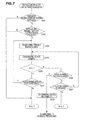
- FIG. 6 is a flowchart of a processing of detecting a bypass abnormality at start-up of an exemplary embodiment.
- FIG. 7 is a flowchart of a processing of detecting a bypass abnormality at an operation of an exemplary embodiment.
- FIG. 8 is a circuit diagram of a bypass unit according to a second exemplary embodiment.
- Exemplary embodiments of a vehicular lamp of the present disclosure will be described. Exemplary embodiments may be used for, for example, a vehicular headlight, and is especially appropriate for a high beam lamp.
- the vehicular lamp 1 includes a light source power supply 10 , a control unit 11 , parallel circuit units 12 A to 12 n , and LEDs 13 A to 13 n .
- FIG. 1 also illustrates a vehicle battery 2 , a lighting switch 3 , and an electronic control unit (“ECU”) 4 .
- ECU electronice control unit
- the parallel circuit units 12 A to 12 n , and the LEDs 13 A to 13 n are collectively referred to as “parallel circuit unit(s) 12 ” and “LED(s) 13 ,” especially when it is not required to distinguish individual ones from others.
- LEDs illustrated as the LEDs 13 A to 13 n are connected in series, as light emitting devices serving as semiconductor light sources.
- the light source power supply 10 causes an emission driving current to flow in the LEDs 13 A to 13 n by a DC voltage from the vehicle battery 2 so that the LEDs 13 A to 13 n are operated to emit light.
- the light source power supply 10 is formed by, for example, a DC-DC converter serving as a switching regulator.
- An input side of the light source power supply 10 is connected to a positive pole and a negative pole (ground) of the vehicle battery 2 via terminals 51 and 52 .
- An output side of the light source power supply 10 is connected to anode terminals and cathode terminals of the n LEDs 13 A to 13 n which constitute a light source, via terminals 53 and 54 . That is, the light source power supply 10 steps up or down the DC voltage between the terminals 51 and 52 to generate an output voltage for a light emission driving of the LEDs 13 A to 13 n and output the output voltage between the terminals 53 and 54 . Accordingly, the light source power supply 10 supplies a light emission driving current to the LEDs 13 A to 13 n .
- a resistor Rs is configured to detect an output current.
- the control unit 11 is constituted by, for example, a microcomputer configured to control the supply of the emission driving current from the light source power supply 10 . That is, the control unit 11 performs an ON/OFF control of a converter operation for the light source power supply 10 , or a switching control (an output current stabilization control by a PWM switching) of the switching regulator when the converter is operated. Specifically, in order to stabilize the output current of the light source power supply 10 , the control unit 11 detects the output current by the voltage across the output current detecting resistor Rs to perform the ON/OFF control of a switching element of the switching regulator according to the detected current. That is, the control unit 11 controls a duty ratio of an ON/OFF control signal of the switching element.
- the control unit 11 may perform a processing of reducing the amount of the emission driving current supplied from the light source power supply 10 , or, in a case of pulse emission, reducing an average emission driving current by controlling the duty ratio of the pulses or a switching frequency.
- a parallel circuit unit 12 includes a bypass unit 20 and an abnormality detecting unit 30 .
- the control unit 11 controls the formation (ON) or the cut-off (OFF) of a bypass route of an emission driving current by the parallel circuit units 12 A to 12 n , and performs an abnormality detection of the bypass route and the LEDs 13 A to 13 n . According to the abnormality detection, the control unit 11 controls the light source power supply 10 to stop or reduce the supply of the emission driving current, or notifies the abnormality to the outside (ECU 4 ).
- the control unit 11 is configured to control the formation and cut-off of a bypass route for each of the parallel circuit units 12 A to 12 n , and may control the turn-ON/OFF of each of the LEDs 13 A to 13 n .
- An abnormality detecting circuit is further provided in each of the parallel circuit units 12 A to 12 n , so that the control unit 11 may detect a route abnormality of the LED side or a bypass abnormality.
- the control unit 11 controls the parallel circuit units 12 A to 12 n so that each of the parallel circuit units 12 A to 12 n controls a light emission operation of corresponding one of the LEDs 13 A to 13 n . That is, when a bypass route formed by a parallel circuit unit 12 is continuously turned ON, a corresponding LED 13 is turned OFF, and when the bypass route is continuously turned OFF, the corresponding LED 13 is turned ON. Also, the bypass route may be turned ON/OFF at a high frequency (e.g., several hundreds of Hz) to dim the corresponding LED 13 . Further, the dimming may be performed by changing the ON-duty in the ON/OFF control.
- the parallel circuit units 12 A to 12 n are configured to detect not only the LED 13 side abnormality but also an abnormality where a current cannot bypass in the bypass route.
- FIG. 2 illustrates a configuration of the parallel circuit unit 12 in the first exemplary embodiment.
- the parallel circuit unit 12 is connected in parallel to the LED 13 , and has a circuit configuration which is largely divided into the bypass unit 20 and the abnormality detecting unit 30 .
- the bypass unit 20 includes a level shift circuit 21 , a gate driving circuit 22 , and a bypass switch 23 constituted by a metal oxide semiconductor-field effect transistor (MOS-FET). Although an N channel MOS-FET is used for the bypass switch 23 , a P channel MOS-FET may be used as well.
- MOS-FET metal oxide semiconductor-field effect transistor
- the drain-source of the bypass switch 23 is connected in parallel to the anode-cathode of the LED 13 .
- a bypass control signal S 1 is supplied to a terminal 24 from the control unit 11 .
- the level of the bypass control signal S 1 is adjusted by the level shift circuit 21 so that the bypass control signal S 1 is given as a gate voltage to the bypass switch 23 by the gate driving circuit 22 .
- the level shift is performed because the LEDs 13 A to 13 n and the parallel circuit units 12 A to 12 n are connected in parallel, respectively, and as a result, the voltage of each of the bypass units 20 and the abnormality detecting units 30 is floating from a reference voltage (a ground voltage).
- the level shift circuit 21 performs the level shift for a gate driving to increase the voltage
- the level shift circuit 21 performs the level shift to reduce the voltage.
- the polarity of the output of the light source power supply 10 is negative.
- the bypass control signal S 1 serves as a control signal for a turn-ON instruction when its level is high (level H) and as a control signal for a turn-OFF instruction when its level is low (level L). That is, the gate driving circuit 22 is configured such that, when the bypass control signal S 1 is in the level H, the gate voltage becomes the level L so that the bypass switch 23 is turned OFF. In this case, the bypass route is cut off, that is, the LED 13 is turned ON. Meanwhile, when the bypass control signal S 1 is in the level L, the gate voltage becomes the level H so that the bypass switch 23 is turned ON. In this case, the bypass route is formed, that is, the LED 13 is turned OFF.
- the abnormality detecting unit 30 is configured as a circuit capable of detecting an abnormality of the LED 13 side (“light-emitting side abnormality”), and an abnormality of the bypass unit 20 (“bypass abnormality”).
- the light-emitting side abnormality refers to, for example, a short-circuit, an open-circuit (disconnection), or harness opening of the LED 13 , or a wiring abnormality between the terminals 53 and 54 of the light source power supply 10 and the LED 13 .
- the bypass abnormality refers to an abnormality of a bypass element such as the level shift circuit 21 , the gate driving circuit 22 , and the bypass switch 23 , that is an event where an emission driving current cannot bypass.
- the bypass abnormality refers to, for example, an opening failure of the bypass switch 23 or a failure of the gate driving circuit 22 .
- the abnormality detecting unit 30 includes NPN-type transistors Q 1 and Q 2 , resistors R 1 to R 5 , a Zener diode ZD, diodes D 1 and D 2 , and a condenser C 1 .
- the resistors R 1 and R 2 divide a drain-source voltage of the bypass switch 23 as a series circuit of the resistors R 1 and R 2 is connected between the drain and the source of the bypass switch 23 .
- a voltage division node of the resistors R 1 and R 2 is connected to the collector of the transistor Q 1 and the base of the transistor Q 2 .
- the cathode of the Zener diode ZD is connected to the anode side of the LED 13 , and the anode side of the Zener diode ZD is connected to the base of the transistor Q 1 via the resistor R 4 .
- a Zener voltage of the Zener diode ZD is set to be higher than a forward voltage Vf of the LED 13 .
- the emitter of the transistor Q 1 is connected to the cathode side of the LED 13 .
- the emitter of the transistor Q 2 is connected to the cathode side of the LED 13 via the resistor R 3 .
- the collector of the transistor Q 2 is connected to a connection point of the cathode of the diodes D 1 and D 2 .
- the anode side of the diode D 1 is grounded, and the anode side of the diode D 2 is connected to a connection point of the resistor R 5 and the condenser C 1 .
- a predetermined voltage Vcc is applied to the resistor R 5 .
- a state signal SD for the control unit 11 is output from the connection point of the resistor R 5 and the condenser C 1 .
- the state signal SD is a signal indicating an abnormal state or a normal state, that is, an abnormality detecting signal.
- the diodes D 1 , D 2 are connected as described above so that the state signal SD to be supplied to the control unit 11 does not become a negative voltage.
- the abnormality detecting unit 30 performs an abnormality detection based on a drain-source voltage Vds of the bypass switch 23 .
- the drain-source voltage Vds in the normal state is about 0 V when the bypass switch 23 is turned ON, and is a forward voltage Vf of the LED 13 when the bypass switch 23 is turned OFF.
- the abnormality detecting unit 30 may output the state signal SD according to the light-emitting side abnormality. Also, even when the bypass abnormality occurs due to the above-described circuit configuration, the abnormality detecting unit 30 may output the state signal SD according the bypass abnormality.
- a specific abnormality detecting operation will be described.
- FIG. 3 illustrates waveforms of respective units in a normal state.
- the control unit 11 sets the level of a bypass control signal S 1 to the level H to make a turn-ON instruction. Accordingly, the bypass switch 23 is turned OFF. In this case, the Zener diode ZD is not conductive.
- the drain-source voltage Vds of the bypass switch 23 becomes Vf, and the voltage division node of the resistors R 1 and R 2 rises so that the transistor Q 2 is turned ON. Accordingly, a sink current SY flows so that the potential at the connection point of the condenser C 1 and the resistor R 5 , that is, the state signal SD becomes the level L.
- the control unit 11 sets the bypass control signal S 1 to be in the low L so as to make a turn-OFF instruction. Accordingly, the bypass switch 23 is turned ON.
- the Zener diode ZD is not conductive.
- the drain-source voltage Vds of the bypass switch 23 becomes about 0V, and the voltage across the voltage division node of the resistors R 1 and R 2 also decreases so that the transistor Q 2 is turned OFF. Accordingly, the sink current SY does not flow and the condenser C 1 is gradually charged so that the state signal SD gradually rises to the level H.
- the control unit 11 may switch the bypass control signal S 1 between the level H and the level L at a high frequency, so that bypass switch 23 is repeatedly turned ON/OFF. That is, the above described turn-ON and turn-OFF states are alternated so that “flowing” and “not-flowing” of the sink current SY will be alternated.
- the condenser C 1 is discharged and the state signal SD becomes the level L.
- the condenser C 1 In a period where the sink current SY does not flow (the period where the voltage across the voltage division node of the resistors R 1 and R 2 becomes about 0V so that the transistor Q 2 is turned OFF), the condenser C 1 is charged and the state signal SD is gradually increased. Meanwhile, by the resistor R 5 and the condenser C 1 , a sufficiently long charging time constant is set for the period of the bypass control signal S 1 . That is, charging is slowly performed and discharging is quickly performed. Accordingly, the state signal SD is maintained in the level L.
- the charging time constant may be set to be several tens of ms
- the discharging time constant may be set to be several hundreds of ⁇ s. Accordingly, at the normal dimming, the level of the state signal SD becomes L.
- FIG. 4 illustrates cases of a light-emitting side abnormality and a bypass abnormality.
- the light-emitting side abnormality is an abnormal state detected when a turn-ON instruction (including a dimming instruction) is made, and the bypass abnormality is an abnormal state detected when a turn-OFF instruction is made.
- FIG. 4 illustrates a case where the light-emitting side abnormality occurs as an example when the dimming is performed.
- the bypass control signal S 1 alternates between the level H and the level L so as to intermittently cut off the bypass route.
- the bypass switch 23 when the bypass switch 23 is turned OFF, the drain-source voltage Vds becomes higher than the forward voltage Vf. Accordingly, the Zener diode ZD is conductive, and the transistor Q 1 is turned ON so that the voltage across the voltage division node does not rise. The transistor Q 2 is turned OFF so that the sink current SY does not flow.
- the drain-source voltage Vds is about 0V, and the voltage across the voltage division node does not rise.
- the transistor Q 2 is turned OFF so that the sink current SY does not flow.
- the level of the state signal SD is gradually increased to the level H.
- the sink current SY does not flow so that the state signal SD also becomes the level H.
- a turn-OFF instruction causes the bypass route to be functioned.
- the control unit 11 makes a turn-OFF instruction by setting the bypass control signal S 1 to be the level L so that the bypass route is continuously formed. Accordingly, the bypass switch 23 is turned ON.
- the drain-source voltage Vds is fixed to be equal to the forward voltage Vf. Accordingly, the voltage across the voltage division node rises and the transistor Q 2 is turned ON so that the sink current SY flows. As a result, the state signal SD also becomes the level L.
- the state signal SD becomes the level L in the normal state.
- an abnormality a light-emitting side abnormality
- the state signal SD becomes the level H in the normal state. However, when an abnormality (a bypass abnormality) occurs, the state signal SD becomes the level L.
- the control unit 11 performs an abnormality detection as follows.
- FIG. 5 illustrates an example of an abnormality detection processing for detecting a light-emitting side abnormality.
- the control unit 11 determines, in step S 101 , whether an emission driving current is currently being supplied from the light source power supply 10 .
- step S 102 the control unit 11 determines whether a turn-ON instruction is being made. That is, it is determined whether the bypass control signal S 1 is output in the level H, or H/L high frequency pulses are output so that turn-ON or dimming is being instructed.
- step S 101 and S 102 when it is determined that the emission driving current is being supplied and the turn-ON instruction is being made, the control unit 11 determines whether the state signal SD is output at the level H in step S 103 . In the normal state, the level of the state signal SD will be in the level L.
- step S 107 when the emission driving current is not being supplied, the turn-ON instruction is not being made, or the state signal SD is in the level L, in step S 107 , an abnormality determination counter CTd is cleared to be 0.
- step S 103 when the state signal SD is in the level H, the control unit 11 , in step S 104 , increments the abnormality determination counter CTd, and then, in step S 105 , determines whether the value of the abnormality determination counter CTd becomes equal to or larger than a predetermined value thE. Unless the value of the abnormality determination counter CTd reaches the predetermined value thE, it is not yet determined that an abnormality occurs. When the value of the abnormality determination counter CTd becomes equal to or larger than the predetermined value thE, in step S 106 , it is determined that the light-emitting side abnormality occurs. Then, a predetermined abnormality handling processing is performed. For example, the control unit 11 stops the supply of the light emission driving current from the light source power supply 10 or notifies the ECU 4 of abnormality occurrence.
- the level H of the state signal SD is continuously observed for a predetermined period during the turn-ON instruction. As a result, the abnormality determination is made.
- the reason of making the abnormality determination based on the fact that the state signal SD is continuously in the level H during the period where the abnormality determination counter CTd reaches the predetermined value is to stabilize the abnormality determination processing.
- FIG. 6 illustrates an example of a processing of detecting a bypass abnormality by the control unit 11 .
- the bypass abnormality is detected in a period where a bypass route is formed by the bypass unit 20 .
- the bypass route formation period refers to a turn-OFF instruction period or an ON period while the bypass switch 23 is turned ON/OFF so as to perform dimming.
- the ON period of the bypass switch 23 ranges from several hundreds of ⁇ s to several msec, and thus it is difficult to detect the bypass abnormality by defining the period. Therefore, the detection is performed when the turn-OFF instruction is made or by providing a turn-OFF instruction period for abnormality detection.
- FIG. 6 illustrates an example of detecting a bypass abnormality when initiating turn-ON.
- the control unit 11 observes a state signal SD output from the abnormality detecting unit 30 for all the parallel circuit units 12 A to 12 n (step S 204 ).
- the state signal SD gradually rises to the level H (see, e.g., the waveform at turn-OFF in FIG. 3 ).
- a certain time period is required until the level of the signal SD becomes the level H by the above described time constant set by the resistor R 5 and the condenser C 1 .
- the control unit 11 determines whether levels of all the state signals SD are in the level H (step S 205 ). When this is not satisfied, the control unit 11 determines whether a predetermined time (a time determined according to the charging time constant of the condenser C 1 ) has elapsed from the initiation of supply of the emission driving current (step S 206 ). When the predetermined time has not elapsed, all the state signals SD are observed again in step S 204 and the determination is performed in step S 205 .
- a predetermined time a time determined according to the charging time constant of the condenser C 1
- step S 207 control the initiation of turn-ON.
- the turn-ON (dimming) of the LEDs 13 A to 13 n is performed by setting the bypass control signal S 1 for each of the parallel circuit units 12 A to 12 n to be the level H (or high frequency pulses).
- control unit 11 proceeds from step S 206 to S 208 , determines that a bypass abnormality occurs, and performs a predetermined abnormality handling processing. For example, the control unit 11 stops the supply of the emission driving current from the light source power supply 10 or notifies the ECU 4 of abnormality occurrence.
- FIG. 7 illustrates an example of detecting a bypass abnormality on a bypass unit 20 which makes a turn-OFF instruction among respective bypass units 20 of the parallel circuit units 12 A to 12 n.
- the control unit 11 determines, in step S 301 , whether an emission driving current is currently being supplied from the light source power supply 10 .
- step S 302 the control unit 11 determines whether at least one bypass unit 20 which is making a turn-OFF instruction is currently present. That is, it is determined whether a bypass control signal S 1 with the level L is given to the at least one bypass unit 20 .
- the emission driving current is not being supplied, or the turn-ON instruction (including a dimming instruction) is being made on the bypass units 20 of all the parallel circuit units 12 A to 12 n , the detection of bypass abnormality is not performed.
- step S 303 When a turn-OFF instruction is made on one or more bypass units 20 , the control unit 11 , in step S 303 , selects one bypass unit 20 as a detection target among the bypass units 20 which are making turn-OFF instructions. In step S 304 , a state signal SD related to the selected bypass unit 20 and output from the abnormality detecting unit 30 is observed.
- the state signal SD When the bypass route is normally formed, the state signal SD is in the level H. However, in consideration of the charging time constant of the condenser C 1 , even if the state signal SD is in the level L, it is not yet determined that there is a bypass abnormality until a predetermined time elapses in step S 306 .
- the predetermined time may be counted from a point of time the process proceeds to step S 303 , or may be counted from a point of time a turn-OFF instruction is initiated for the bypass unit 20 .
- the turn-ON situation may be changed by an operation of a vehicle driver or an instruction from the ECU 4 .
- the LED 13 may be switched from turn-OFF to turn-ON.
- the abnormality detection processing is finished from step S 307 .
- step S 304 When the predetermined time has not elapsed and there is no change in the situation, the process proceeds back to step S 304 to observe the state signal SD again.
- step S 309 When it is determined that the predetermined time has elapsed in step S 306 while the state signal SD remains at the level L, it is determined, in step S 309 , that a bypass abnormality occurs, to perform a predetermined abnormality handling processing.
- the control unit 11 stops the supply of the emission driving current from the light source power supply 10 or notifies the ECU 4 of abnormality occurrence.
- step S 308 it is determined whether there is any non-determined bypass unit 20 which is making a turn-OFF instruction.
- the bypass unit 20 is selected as a detection target in step S 303 and the same processing as described above is performed on the bypass unit 20 as well.
- the vehicular lamp includes: a plurality of LEDs 13 ( 13 A to 13 n ) connected in series; a light source power supply 10 configured to supply an emission driving current to the plurality of LEDs 13 ; a bypass unit 20 connected in parallel to each of the LEDs 13 to form a bypass route of an emission driving current so as to cause the LEDs 13 to be in a turn-OFF state according to a bypass control signal S 1 , or to cut off the bypass route of the emission driving current so as to cause the LEDs 13 to be in a turn-ON state; and an abnormality detecting unit 30 configured to generate a state signal SD indicating whether the bypass unit 20 is in an abnormal state or a normal state. When a signal indicating that the bypass unit 20 is abnormal is generated as the state signal SD, the emission driving current supplied from the light source power supply 10 is reduced or stopped.
- the abnormal state of the bypass unit 20 may be detected by the abnormality detecting unit 30 to determine a bypass abnormality.
- the LEDs 13 connected in parallel to the bypass unit 20 cannot be turned OFF.
- the turn-OFF of a high beam cannot be performed and as a result, glare is given to an oncoming vehicle.
- the supply of the emission driving current may be reduced or stopped according to the detection of the bypass abnormality so that the problem itself may be suppressed.
- the state signal SD generated by the abnormality detecting unit 30 indicates the normal state of the light emitting device side by the level L (first logic level) and indicates the abnormality at the light-emitting side by the level H (second logic level).
- the period in which continuous or intermittent cut-off of a bypass route is instructed by the bypass control signal S 1 refers to a period in which a turn-ON instruction or a dimming instruction is made to perform the turn-ON or dimming of the LEDs 13 .
- the LEDs 13 serving as light emitting devices should be in the turn-ON state or dimming state.
- the LEDs 13 are in the turn-OFF state, it should be detected as an abnormal state. Therefore, in the present exemplary embodiment, the abnormal/normal state of the light emitting device side is determined by the state signal SD.
- the state signal SD indicates the normal state of the bypass unit 20 by the level H (second logic level) and indicates an abnormal state of the bypass unit 20 by the level L (first logic level).
- the period in which the continuous formation of a bypass route is instructed by the bypass control signal S 1 refers to a period in which a turn-OFF instruction is made to perform the turn-OFF of the LEDs 13 .
- the LEDs 13 serving as light emitting devices should be in the turn-OFF state.
- the LEDs 13 are not in the turn-OFF state, it should be detected as a bypass abnormal state. Therefore, in the present exemplary embodiment, the abnormal/normal state of the bypass unit 20 is determined by the state signal SD.
- an abnormality detection function of the abnormality detecting unit 30 may be separately used so that the function of detecting the light-emitting side abnormality and the function of detecting the bypass abnormality may be properly exhibited.
- this may also simplify the circuit configuration of the abnormality detecting unit 30 .
- the control unit 11 performs a detection corresponding to reversal of determination logics, both the detection of a bypass abnormality and the detection of a light-emitting side abnormality are enabled with a simple circuit configuration of generating a state signal SD based on a drain-source voltage of the bypass switch 23 .
- bypass control signals S 1 on all the bypass units 20 when the supply of the emission driving current is initiated by the light source power supply 10 , a formation control of bypass routes (turn-OFF instructions) is performed by bypass control signals S 1 on all the bypass units 20 .
- the formation control when at least one of state signals SD output from the abnormality detecting units 30 corresponding to the respective bypass units 20 continuously indicates an abnormal state of the corresponding bypass unit for a predetermined time, it is determined that the bypass units are in the abnormal state.
- bypass abnormality detection When the bypass abnormality detection is performed for a period during which the turn-OFF instruction is made, it becomes suitable to determine the bypass abnormality, for example, at a point of time of initiating a turn-ON. This is because after the turn-ON is initiated, it is difficult to perform an operation of turning OFF so as to detect an abnormality. Also, when at least one of the plurality of bypass units 20 is abnormal, a proper handling control to prevent occurrence of the above-described glare may be performed by determining it as a bypass abnormality state.
- a bypass unit 20 which performs a formation control (a turn-OFF instruction) of a bypass route by a bypass control signal S 1 during the supply of the emission driving current by the light source power supply 10 , when a state signal SD output from an abnormality detecting unit 30 corresponding to the bypass unit 20 continuously indicates an abnormal state for a predetermined time, it is determined that the bypass unit is abnormal.
- control unit 11 performs processings of controlling the supply of the emission driving current by the light source power supply 10 , outputting the bypass control signal S 1 to the bypass unit 20 , and detecting the bypass abnormality and the light-emitting side abnormality by monitoring the state signal SD. Then, when detecting the bypass abnormality or the light-emitting side abnormality according to the state signal SD, the control unit 11 controls the reduction or stopping of supply of the emission driving current from the light source power supply 10 .
- the detection of bypass abnormality and light-emitting side abnormality or the abnormality handling processing may be properly performed. In particular, as illustrated in FIGS.
- the control unit 11 may perform a detection of the light-emitting side abnormality and the bypass abnormality by reversing determination logics on the state signal SD. Therefore, it is possible to handle both the detection of a bypass abnormality and the detection of a light-emitting side abnormality by the abnormality detecting unit 30 configured according to the present exemplary embodiment, which may contribute to reduction of a circuit scale.
- the control unit 11 observes a state signal SD to detect both the light-emitting side abnormality and the bypass abnormality through software processing in which the detection of the bypass abnormality is achieved by forcedly making a turn-OFF instruction in a period where a turn-OFF instruction is made or when initiating the detection.
- the second exemplary embodiment is an example in which the light-emitting side abnormality and the bypass abnormality are separately detected by means of hardware so as to detect the bypass abnormality in real time.
- FIG. 8 illustrates one LED 13 in the configuration of FIG. 1 , and a parallel circuit unit 12 corresponding to the LED 13 , in which the parallel circuit unit 12 includes a bypass unit 20 and an abnormality detecting unit 30 .
- the abnormality detecting unit 30 is constituted by a first circuit unit 30 A and a second circuit unit 30 B.
- the bypass unit 20 has a configuration which is the same as that in FIG. 2 .
- the first circuit unit 30 A is the same as the abnormality detecting unit 30 in FIG. 2 . That is, the configuration of FIG. 8 may be a configuration formed by adding a second circuit unit 30 B and a peripheral circuit thereof to the configuration of FIG. 2 .
- a state signal SDa output by the first circuit unit 30 A is a signal which is the same as the state signal SD in the first exemplary embodiment.
- the state signal SDA is used as a detecting signal of a light-emitting side abnormality. That is, the state signal SDa may indicate that the light-emitting side is abnormal by the level H and that the light-emitting side is normal by the level L (see, e.g., FIGS. 3 and 4 ).
- FIG. 8 a configuration in FIG. 8 which is different from that in FIG. 2 will be described.
- the second circuit unit 30 B includes PNP-type transistors Q 3 and Q 4 , resistors R 10 to R 13 , diodes D 3 and D 4 , and a condenser C 2 .
- the resistors R 10 , R 11 and R 12 are connected in series to a route of a sink current SY (a collector of the transistor Q 2 ).
- the base is connected to a connection point of the resistors R 10 and R 11
- the emitter is connected to a connection point of the resistors R 11 and R 12
- the collector is grounded.
- the anode of the diode D 3 is connected to the terminal 24 to which a bypass control signal S 1 of a bypass unit 20 is input, and the condenser C 2 is connected between the cathode side and the ground.
- the connection point of the diode D 3 and the condenser C 2 is connected to the resistor R 12 and the base of the transistor Q 4 .
- the emitter of the transistor Q 4 is connected to a predetermined voltage Vcc line via the diode D 4 .
- the bias resistor R 13 is connected between the base and the emitter of the transistor Q 4 .
- the collector output of the transistor Q 4 becomes a state signal SDb′ for detecting a bypass abnormality.
- the state signal SDb′ indicates a bypass abnormality by the level H, and a normality by the level L.
- the same configuration is employed in the plurality of parallel circuit units 12 A to 12 n , and a state signal SDb′ output from each second circuit unit 30 B is supplied to the connection point of the resistors R 14 and R 15 in a wired OR form.
- the output of a low pass filter by the condenser C 3 is supplied to the control unit 11 as a state signal SDb.
- the state signal SDb becomes the level H when a bypass abnormality exists in at least one of the parallel circuit units 12 A to 12 n
- the state signal SDb becomes the level L when all of the parallel circuit units 12 A to 12 n are normal.
- the transistor Q 3 In a period where the sink current SY flows (the ON period of the transistor Q 2 ), the transistor Q 3 is turned ON to discharge the condenser C 2 .
- the diode D 3 is conductive when the bypass control signal S 1 becomes the level H to charge the condenser C 2 . Accordingly, at a normal state, when the bypass control signal S 1 becomes the level H and thus a turn-ON instruction is made, the sink current SY flows to discharge the condenser C 2 , while quick charging is performed at the diode D 3 side of the condenser C 2 so that the charged state of the condenser C 2 is maintained.
- the sink current SY does not flow and the transistor Q 3 is turned OFF.
- the cathode side of the diode D 3 is connected, there is no discharge route of the condenser C 2 .
- the charged state of the condenser C 2 is maintained.
- the transistor Q 4 is suppressed from being turned ON.
- the transistor Q 4 is turned OFF, the potential of the connection point of the resistors R 14 and R 15 becomes the level L, and the state signal SDb becomes the level L.
- the condenser C 2 is set to be quickly charged and slowly discharged. Accordingly, when a bypass abnormality occurs in a case where a bypass control signal S 1 with high frequency pulses is given during a dimming instruction, that is, when a bypass route is not formed in the L-level period of the bypass control signal S 1 , the state signal SDb with the level H may be obtained.
- the abnormality detecting unit 30 includes the first circuit unit 30 A and the second circuit unit 30 B.
- the first circuit unit 30 A generates a first state signal SDa indicating a normal state or an abnormal state of the LED 13 side in a period where the bypass unit 20 is instructed to cut off the bypass route by the bypass control signal S 1 (in a turn-ON instruction or dimming instruction period) during the supply of the emission driving current by the light source power supply 10 .
- the second circuit unit 30 B generates a second state signal SDb indicating a normal state or an abnormal state of the bypass unit 20 , irrespective of the state of control by the bypass control signal S 1 during the supply of the emission driving current by the light source power supply 10 .
- the bypass abnormality may be always detected irrespective of the control state by the bypass control signal S 1 .
- one parallel circuit unit 12 may be provided for a group of serial or parallel LEDs.
- the parallel circuit unit 12 may not be formed for all the LEDs 13 . Especially, it is preferable that the parallel circuit unit 12 is provided for some LEDs 13 which may be turned OFF or dimmed during the supply of a current by the light source power supply 10 .
- the present disclosure may also be applied to a case where other types of light emitting devices such as, for example, a filament bulb is used without being limited to a case where a semiconductor light emitting device such as, for example, an LED, is used.
- control unit 11 performs a control of stopping or reducing the supply of the emission driving current from the light source power supply 10 , or a processing of making a notification to the ECU 4 when detecting an abnormality.
- control unit 11 may perform an abnormality handling processing.
- the handling processing contents may be changed to each other.
- the control unit 11 or the function of detecting a bypass abnormality by monitoring a state signal may be provided outside of the vehicular lamp 1 (for example, in a vehicle side microcomputer).
- the vehicular lamp of the present disclosure may be applied to, for example, a tail lamp, a daytime running lamp, a cornering lamp, a turn signal lamp, and a break lamp, besides the headlight.
- the technology of the present disclosure may also be applied to various lighting devices as non-vehicular lamps.
Landscapes
- Engineering & Computer Science (AREA)
- Mechanical Engineering (AREA)
- Lighting Device Outwards From Vehicle And Optical Signal (AREA)
Applications Claiming Priority (2)
| Application Number | Priority Date | Filing Date | Title |
|---|---|---|---|
| JP2013-252847 | 2013-12-06 | ||
| JP2013252847A JP6199721B2 (ja) | 2013-12-06 | 2013-12-06 | 車両用灯具 |
Publications (2)
| Publication Number | Publication Date |
|---|---|
| US20150163871A1 US20150163871A1 (en) | 2015-06-11 |
| US9320107B2 true US9320107B2 (en) | 2016-04-19 |
Family
ID=53272561
Family Applications (1)
| Application Number | Title | Priority Date | Filing Date |
|---|---|---|---|
| US14/559,049 Active US9320107B2 (en) | 2013-12-06 | 2014-12-03 | Vehicular lamp |
Country Status (3)
| Country | Link |
|---|---|
| US (1) | US9320107B2 (zh) |
| JP (1) | JP6199721B2 (zh) |
| CN (2) | CN104703336B (zh) |
Cited By (1)
| Publication number | Priority date | Publication date | Assignee | Title |
|---|---|---|---|---|
| KR20030037698A (ko) * | 2001-11-05 | 2003-05-16 | 송치호 | 용기바닥에 웅덩이 홈이 형성된 취출이 용이한 액체저장용기 |
Families Citing this family (22)
| Publication number | Priority date | Publication date | Assignee | Title |
|---|---|---|---|---|
| JP6240587B2 (ja) * | 2014-10-30 | 2017-11-29 | 矢崎総業株式会社 | 断線検出装置および断線検出方法 |
| DE112015004904T5 (de) | 2014-10-30 | 2017-07-20 | Yazaki Corporation | Fahrzeugenergieversorgungssteuervorrichtung |
| JP6641080B2 (ja) * | 2014-11-05 | 2020-02-05 | ローム株式会社 | 発光素子駆動装置、発光装置、車両 |
| JP6185941B2 (ja) * | 2015-01-23 | 2017-08-23 | 矢崎総業株式会社 | 照明制御システム |
| JP6688008B2 (ja) * | 2015-04-07 | 2020-04-28 | 株式会社小糸製作所 | 車両用灯具 |
| JP6779879B2 (ja) | 2015-07-30 | 2020-11-04 | 株式会社小糸製作所 | 点灯回路、車両用灯具 |
| JP6723064B2 (ja) * | 2016-05-10 | 2020-07-15 | ローム株式会社 | 地絡検出回路、異常検出回路、発光装置、車両 |
| US10426013B2 (en) | 2016-05-10 | 2019-09-24 | Rohm Co., Ltd. | Ground fault detection circuit, abnormality detection circuit, light emitting device, vehicle |
| JP6811051B2 (ja) * | 2016-07-29 | 2021-01-13 | 株式会社小糸製作所 | 点灯回路および車両用灯具 |
| JP6849342B2 (ja) * | 2016-08-16 | 2021-03-24 | 株式会社小糸製作所 | 点灯回路および車両用灯具 |
| DE102016225800B3 (de) | 2016-12-21 | 2018-05-30 | Lear Corporation | Verfahren zum überwachen des betriebszustands einer led in einer fahrzeugleuchtenanordnung |
| CN106879148A (zh) * | 2017-03-29 | 2017-06-20 | 上海小糸车灯有限公司 | 一种信号灯的控制系统及方法 |
| JP6933548B2 (ja) * | 2017-05-11 | 2021-09-08 | 株式会社小糸製作所 | 駆動回路、車両用灯具 |
| CN109152125A (zh) * | 2017-06-28 | 2019-01-04 | 群光电能科技股份有限公司 | 发光装置及其驱动方法 |
| JP7000840B2 (ja) * | 2017-12-19 | 2022-01-19 | 株式会社デンソー | 車両用前方照明装置 |
| JP7024388B2 (ja) * | 2017-12-22 | 2022-02-24 | 株式会社デンソー | 車両用前方照明装置、断線検出方法 |
| JP6988467B2 (ja) * | 2017-12-27 | 2022-01-05 | 株式会社デンソー | 車両用前方照明装置、断線検出方法 |
| JP7102909B2 (ja) * | 2018-04-27 | 2022-07-20 | 市光工業株式会社 | 車両用灯具 |
| CN112566817A (zh) * | 2018-08-27 | 2021-03-26 | 株式会社小糸制作所 | 点亮电路及车辆用灯具 |
| JP7220056B2 (ja) * | 2018-11-08 | 2023-02-09 | ナブテスコ株式会社 | 通知装置及びドア開閉装置 |
| JP7430188B2 (ja) | 2019-08-01 | 2024-02-09 | 株式会社小糸製作所 | 灯具モジュールおよびその点灯回路 |
| JP7408448B2 (ja) * | 2020-03-18 | 2024-01-05 | 株式会社小糸製作所 | 光源モジュールおよび点灯回路 |
Citations (10)
| Publication number | Priority date | Publication date | Assignee | Title |
|---|---|---|---|---|
| US20070132602A1 (en) * | 2005-12-12 | 2007-06-14 | Koito Manufacturing Co., Ltd. | Vehicle lighting apparatus |
| US7710050B2 (en) * | 2005-11-17 | 2010-05-04 | Magna International Inc | Series connected power supply for semiconductor-based vehicle lighting systems |
| US20110148306A1 (en) * | 2009-12-18 | 2011-06-23 | Ampower Technology Co., Ltd. | Bypass protection circuit and light emitting diode driving device using the same |
| JP2011192865A (ja) | 2010-03-16 | 2011-09-29 | Koito Mfg Co Ltd | 点灯制御装置及び車両用灯具 |
| US20120025713A1 (en) * | 2010-07-30 | 2012-02-02 | International Rectifier Corporation | System using shunt circuits to selectively bypass open loads |
| JP2013109939A (ja) | 2011-11-21 | 2013-06-06 | Koito Mfg Co Ltd | 半導体光源点灯回路 |
| US20130200802A1 (en) * | 2012-02-03 | 2013-08-08 | Nichia Corporation | Light-emitting diode driving apparatus |
| US20130200801A1 (en) * | 2012-02-02 | 2013-08-08 | Roger Fratti | BYPASS CIRCUIT FOR SERIES CONNECTED LEDs USED FOR BACKLIGHTING |
| US20140265890A1 (en) * | 2013-03-14 | 2014-09-18 | Koito Manufacturing Co., Ltd. | Light source control device |
| US20150173133A1 (en) * | 2013-12-18 | 2015-06-18 | Panasonic Intellectual Property Management Co., Ltd. | Lighting device and luminaire |
Family Cites Families (7)
| Publication number | Priority date | Publication date | Assignee | Title |
|---|---|---|---|---|
| JP4241487B2 (ja) * | 2004-04-20 | 2009-03-18 | ソニー株式会社 | Led駆動装置、バックライト光源装置及びカラー液晶表示装置 |
| JP2008251276A (ja) * | 2007-03-29 | 2008-10-16 | Stanley Electric Co Ltd | 発光ダイオード回路の故障検知装置 |
| KR100956222B1 (ko) * | 2008-10-30 | 2010-05-04 | 삼성전기주식회사 | 멀티 발광 소자의 구동 장치 |
| CN102014544B (zh) * | 2010-07-13 | 2014-04-16 | 深圳市航嘉驰源电气股份有限公司 | Led灯驱动电路 |
| CN101894873B (zh) * | 2010-08-04 | 2012-01-04 | 王磊 | 一种具有故障检测装置的光伏阵列组件 |
| CN104303602B (zh) * | 2012-05-18 | 2016-08-17 | 株式会社小糸制作所 | 光源控制装置 |
| US9253850B2 (en) * | 2012-05-22 | 2016-02-02 | Texas Instruments Incorporated | LED bypass and control circuit for fault tolerant LED systems |
-
2013
- 2013-12-06 JP JP2013252847A patent/JP6199721B2/ja active Active
-
2014
- 2014-12-01 CN CN201410718753.6A patent/CN104703336B/zh active Active
- 2014-12-01 CN CN201711030051.9A patent/CN107734802B/zh active Active
- 2014-12-03 US US14/559,049 patent/US9320107B2/en active Active
Patent Citations (10)
| Publication number | Priority date | Publication date | Assignee | Title |
|---|---|---|---|---|
| US7710050B2 (en) * | 2005-11-17 | 2010-05-04 | Magna International Inc | Series connected power supply for semiconductor-based vehicle lighting systems |
| US20070132602A1 (en) * | 2005-12-12 | 2007-06-14 | Koito Manufacturing Co., Ltd. | Vehicle lighting apparatus |
| US20110148306A1 (en) * | 2009-12-18 | 2011-06-23 | Ampower Technology Co., Ltd. | Bypass protection circuit and light emitting diode driving device using the same |
| JP2011192865A (ja) | 2010-03-16 | 2011-09-29 | Koito Mfg Co Ltd | 点灯制御装置及び車両用灯具 |
| US20120025713A1 (en) * | 2010-07-30 | 2012-02-02 | International Rectifier Corporation | System using shunt circuits to selectively bypass open loads |
| JP2013109939A (ja) | 2011-11-21 | 2013-06-06 | Koito Mfg Co Ltd | 半導体光源点灯回路 |
| US20130200801A1 (en) * | 2012-02-02 | 2013-08-08 | Roger Fratti | BYPASS CIRCUIT FOR SERIES CONNECTED LEDs USED FOR BACKLIGHTING |
| US20130200802A1 (en) * | 2012-02-03 | 2013-08-08 | Nichia Corporation | Light-emitting diode driving apparatus |
| US20140265890A1 (en) * | 2013-03-14 | 2014-09-18 | Koito Manufacturing Co., Ltd. | Light source control device |
| US20150173133A1 (en) * | 2013-12-18 | 2015-06-18 | Panasonic Intellectual Property Management Co., Ltd. | Lighting device and luminaire |
Cited By (1)
| Publication number | Priority date | Publication date | Assignee | Title |
|---|---|---|---|---|
| KR20030037698A (ko) * | 2001-11-05 | 2003-05-16 | 송치호 | 용기바닥에 웅덩이 홈이 형성된 취출이 용이한 액체저장용기 |
Also Published As
| Publication number | Publication date |
|---|---|
| CN107734802A (zh) | 2018-02-23 |
| JP6199721B2 (ja) | 2017-09-20 |
| JP2015110357A (ja) | 2015-06-18 |
| CN104703336B (zh) | 2017-12-01 |
| US20150163871A1 (en) | 2015-06-11 |
| CN107734802B (zh) | 2019-09-27 |
| CN104703336A (zh) | 2015-06-10 |
Similar Documents
| Publication | Publication Date | Title |
|---|---|---|
| US9320107B2 (en) | Vehicular lamp | |
| CN108650747B (zh) | 点灯电路及使用该点灯电路的车辆用灯具 | |
| US10081301B2 (en) | Lighting circuit and vehicular turn signal lamp | |
| JP5161040B2 (ja) | 車両用灯具の点灯制御装置 | |
| JP4776596B2 (ja) | 車両用灯具の点灯制御装置 | |
| US9992835B2 (en) | Lighting circuit | |
| US8222839B2 (en) | Dimming control system for vehicular lamp | |
| JP5275450B2 (ja) | 直流電源照明システム用の低損失型入力チャネル検出装置 | |
| US20100117656A1 (en) | Led outage detection circuit | |
| US9162607B2 (en) | Vehicular lamp | |
| JP2007200610A (ja) | 車両用灯具の点灯制御装置 | |
| JP6783790B2 (ja) | 点灯回路、車両用灯具 | |
| US9531157B2 (en) | Lighting circuit and lamp system | |
| JP6302706B2 (ja) | 車両用灯具およびその駆動装置 | |
| EP2410820A2 (en) | Semiconductor light source lighting circuit and control method | |
| US20180339641A1 (en) | Lighting circuit and vehicle lamp | |
| US11229102B2 (en) | Lighting device | |
| US11464100B2 (en) | Vehicle headlight system | |
| JP2013109939A (ja) | 半導体光源点灯回路 | |
| WO2023106199A1 (ja) | 点灯回路、及び車両用灯具 | |
| KR102016718B1 (ko) | 차량용 램프 제어 장치 | |
| JP2007022127A (ja) | 車両用灯具の点灯制御装置 | |
| JP2015080999A (ja) | 車両用灯具 |
Legal Events
| Date | Code | Title | Description |
|---|---|---|---|
| AS | Assignment |
Owner name: KOITO MANUFACTURING CO., LTD., JAPAN Free format text: ASSIGNMENT OF ASSIGNORS INTEREST;ASSIGNORS:TAKESHI, TODA;MURAMATSU, TAKAO;TOSHIYUKI, TSUCHIYA;AND OTHERS;REEL/FRAME:034358/0153 Effective date: 20141201 |
|
| STCF | Information on status: patent grant |
Free format text: PATENTED CASE |
|
| MAFP | Maintenance fee payment |
Free format text: PAYMENT OF MAINTENANCE FEE, 4TH YEAR, LARGE ENTITY (ORIGINAL EVENT CODE: M1551); ENTITY STATUS OF PATENT OWNER: LARGE ENTITY Year of fee payment: 4 |
|
| FEPP | Fee payment procedure |
Free format text: MAINTENANCE FEE REMINDER MAILED (ORIGINAL EVENT CODE: REM.); ENTITY STATUS OF PATENT OWNER: LARGE ENTITY |