US9209527B2 - Joining method, joint structure, electronic device, method for manufacturing electronic device and electronic part - Google Patents
Joining method, joint structure, electronic device, method for manufacturing electronic device and electronic part Download PDFInfo
- Publication number
- US9209527B2 US9209527B2 US13/904,072 US201313904072A US9209527B2 US 9209527 B2 US9209527 B2 US 9209527B2 US 201313904072 A US201313904072 A US 201313904072A US 9209527 B2 US9209527 B2 US 9209527B2
- Authority
- US
- United States
- Prior art keywords
- metal
- melting point
- joining
- metal member
- low melting
- Prior art date
- Legal status (The legal status is an assumption and is not a legal conclusion. Google has not performed a legal analysis and makes no representation as to the accuracy of the status listed.)
- Active, expires
Links
Images


Classifications
-
- B—PERFORMING OPERATIONS; TRANSPORTING
- B23—MACHINE TOOLS; METAL-WORKING NOT OTHERWISE PROVIDED FOR
- B23K—SOLDERING OR UNSOLDERING; WELDING; CLADDING OR PLATING BY SOLDERING OR WELDING; CUTTING BY APPLYING HEAT LOCALLY, e.g. FLAME CUTTING; WORKING BY LASER BEAM
- B23K35/00—Rods, electrodes, materials, or media, for use in soldering, welding, or cutting
- B23K35/02—Rods, electrodes, materials, or media, for use in soldering, welding, or cutting characterised by mechanical features, e.g. shape
- B23K35/0222—Rods, electrodes, materials, or media, for use in soldering, welding, or cutting characterised by mechanical features, e.g. shape for use in soldering or brazing
- B23K35/0233—Sheets or foils
- B23K35/0238—Sheets or foils layered
-
- H—ELECTRICITY
- H01—ELECTRIC ELEMENTS
- H01R—ELECTRICALLY-CONDUCTIVE CONNECTIONS; STRUCTURAL ASSOCIATIONS OF A PLURALITY OF MUTUALLY-INSULATED ELECTRICAL CONNECTING ELEMENTS; COUPLING DEVICES; CURRENT COLLECTORS
- H01R4/00—Electrically-conductive connections between two or more conductive members in direct contact, i.e. touching one another; Means for effecting or maintaining such contact; Electrically-conductive connections having two or more spaced connecting locations for conductors and using contact members penetrating insulation
- H01R4/02—Soldered or welded connections
-
- B—PERFORMING OPERATIONS; TRANSPORTING
- B23—MACHINE TOOLS; METAL-WORKING NOT OTHERWISE PROVIDED FOR
- B23K—SOLDERING OR UNSOLDERING; WELDING; CLADDING OR PLATING BY SOLDERING OR WELDING; CUTTING BY APPLYING HEAT LOCALLY, e.g. FLAME CUTTING; WORKING BY LASER BEAM
- B23K1/00—Soldering, e.g. brazing, or unsoldering
- B23K1/0008—Soldering, e.g. brazing, or unsoldering specially adapted for particular articles or work
- B23K1/0016—Soldering of electronic components
-
- B—PERFORMING OPERATIONS; TRANSPORTING
- B23—MACHINE TOOLS; METAL-WORKING NOT OTHERWISE PROVIDED FOR
- B23K—SOLDERING OR UNSOLDERING; WELDING; CLADDING OR PLATING BY SOLDERING OR WELDING; CUTTING BY APPLYING HEAT LOCALLY, e.g. FLAME CUTTING; WORKING BY LASER BEAM
- B23K1/00—Soldering, e.g. brazing, or unsoldering
- B23K1/19—Soldering, e.g. brazing, or unsoldering taking account of the properties of the materials to be soldered
-
- B—PERFORMING OPERATIONS; TRANSPORTING
- B23—MACHINE TOOLS; METAL-WORKING NOT OTHERWISE PROVIDED FOR
- B23K—SOLDERING OR UNSOLDERING; WELDING; CLADDING OR PLATING BY SOLDERING OR WELDING; CUTTING BY APPLYING HEAT LOCALLY, e.g. FLAME CUTTING; WORKING BY LASER BEAM
- B23K35/00—Rods, electrodes, materials, or media, for use in soldering, welding, or cutting
- B23K35/02—Rods, electrodes, materials, or media, for use in soldering, welding, or cutting characterised by mechanical features, e.g. shape
- B23K35/0222—Rods, electrodes, materials, or media, for use in soldering, welding, or cutting characterised by mechanical features, e.g. shape for use in soldering or brazing
- B23K35/0244—Powders, particles or spheres; Preforms made therefrom
-
- B—PERFORMING OPERATIONS; TRANSPORTING
- B23—MACHINE TOOLS; METAL-WORKING NOT OTHERWISE PROVIDED FOR
- B23K—SOLDERING OR UNSOLDERING; WELDING; CLADDING OR PLATING BY SOLDERING OR WELDING; CUTTING BY APPLYING HEAT LOCALLY, e.g. FLAME CUTTING; WORKING BY LASER BEAM
- B23K35/00—Rods, electrodes, materials, or media, for use in soldering, welding, or cutting
- B23K35/22—Rods, electrodes, materials, or media, for use in soldering, welding, or cutting characterised by the composition or nature of the material
- B23K35/24—Selection of soldering or welding materials proper
- B23K35/26—Selection of soldering or welding materials proper with the principal constituent melting at less than 400°C
- B23K35/262—Sn as the principal constituent
-
- B—PERFORMING OPERATIONS; TRANSPORTING
- B23—MACHINE TOOLS; METAL-WORKING NOT OTHERWISE PROVIDED FOR
- B23K—SOLDERING OR UNSOLDERING; WELDING; CLADDING OR PLATING BY SOLDERING OR WELDING; CUTTING BY APPLYING HEAT LOCALLY, e.g. FLAME CUTTING; WORKING BY LASER BEAM
- B23K35/00—Rods, electrodes, materials, or media, for use in soldering, welding, or cutting
- B23K35/22—Rods, electrodes, materials, or media, for use in soldering, welding, or cutting characterised by the composition or nature of the material
- B23K35/24—Selection of soldering or welding materials proper
- B23K35/30—Selection of soldering or welding materials proper with the principal constituent melting at less than 1550°C
-
- C—CHEMISTRY; METALLURGY
- C22—METALLURGY; FERROUS OR NON-FERROUS ALLOYS; TREATMENT OF ALLOYS OR NON-FERROUS METALS
- C22C—ALLOYS
- C22C13/00—Alloys based on tin
-
- C—CHEMISTRY; METALLURGY
- C22—METALLURGY; FERROUS OR NON-FERROUS ALLOYS; TREATMENT OF ALLOYS OR NON-FERROUS METALS
- C22C—ALLOYS
- C22C13/00—Alloys based on tin
- C22C13/02—Alloys based on tin with antimony or bismuth as the next major constituent
-
- C—CHEMISTRY; METALLURGY
- C22—METALLURGY; FERROUS OR NON-FERROUS ALLOYS; TREATMENT OF ALLOYS OR NON-FERROUS METALS
- C22C—ALLOYS
- C22C9/00—Alloys based on copper
- C22C9/05—Alloys based on copper with manganese as the next major constituent
-
- C—CHEMISTRY; METALLURGY
- C22—METALLURGY; FERROUS OR NON-FERROUS ALLOYS; TREATMENT OF ALLOYS OR NON-FERROUS METALS
- C22C—ALLOYS
- C22C9/00—Alloys based on copper
- C22C9/06—Alloys based on copper with nickel or cobalt as the next major constituent
-
- H—ELECTRICITY
- H01—ELECTRIC ELEMENTS
- H01R—ELECTRICALLY-CONDUCTIVE CONNECTIONS; STRUCTURAL ASSOCIATIONS OF A PLURALITY OF MUTUALLY-INSULATED ELECTRICAL CONNECTING ELEMENTS; COUPLING DEVICES; CURRENT COLLECTORS
- H01R4/00—Electrically-conductive connections between two or more conductive members in direct contact, i.e. touching one another; Means for effecting or maintaining such contact; Electrically-conductive connections having two or more spaced connecting locations for conductors and using contact members penetrating insulation
- H01R4/58—Electrically-conductive connections between two or more conductive members in direct contact, i.e. touching one another; Means for effecting or maintaining such contact; Electrically-conductive connections having two or more spaced connecting locations for conductors and using contact members penetrating insulation characterised by the form or material of the contacting members
-
- H—ELECTRICITY
- H05—ELECTRIC TECHNIQUES NOT OTHERWISE PROVIDED FOR
- H05K—PRINTED CIRCUITS; CASINGS OR CONSTRUCTIONAL DETAILS OF ELECTRIC APPARATUS; MANUFACTURE OF ASSEMBLAGES OF ELECTRICAL COMPONENTS
- H05K3/00—Apparatus or processes for manufacturing printed circuits
- H05K3/30—Assembling printed circuits with electric components, e.g. with resistors
- H05K3/32—Assembling printed circuits with electric components, e.g. with resistors electrically connecting electric components or wires to printed circuits
- H05K3/34—Assembling printed circuits with electric components, e.g. with resistors electrically connecting electric components or wires to printed circuits by soldering
- H05K3/346—Solder materials or compositions specially adapted therefor
-
- H05K3/3463—
-
- B—PERFORMING OPERATIONS; TRANSPORTING
- B23—MACHINE TOOLS; METAL-WORKING NOT OTHERWISE PROVIDED FOR
- B23K—SOLDERING OR UNSOLDERING; WELDING; CLADDING OR PLATING BY SOLDERING OR WELDING; CUTTING BY APPLYING HEAT LOCALLY, e.g. FLAME CUTTING; WORKING BY LASER BEAM
- B23K2101/00—Articles made by soldering, welding or cutting
- B23K2101/36—Electric or electronic devices
- B23K2101/42—Printed circuits
-
- H—ELECTRICITY
- H05—ELECTRIC TECHNIQUES NOT OTHERWISE PROVIDED FOR
- H05K—PRINTED CIRCUITS; CASINGS OR CONSTRUCTIONAL DETAILS OF ELECTRIC APPARATUS; MANUFACTURE OF ASSEMBLAGES OF ELECTRICAL COMPONENTS
- H05K2201/00—Indexing scheme relating to printed circuits covered by H05K1/00
- H05K2201/02—Fillers; Particles; Fibers; Reinforcement materials
- H05K2201/0203—Fillers and particles
- H05K2201/0263—Details about a collection of particles
- H05K2201/0272—Mixed conductive particles, i.e. using different conductive particles, e.g. differing in shape
-
- Y10T403/479—
Definitions
- the present invention relates to a joining method, a joint structure, an electronic device, a method for manufacturing an electronic device, and an electronic part, and more particularly to a joining method which is used in mounting, for example, an electronic part, a joint structure, an electronic device, a method for manufacturing an electronic device, and an electronic part.
- solder paste solder paste
- soldering is performed at a temperature of 330 to 350° C. by using Pb-rich Pb-5Sn (melting point: 314 to 310° C.) or Pb-10Sn (melting point: 302 to 275° C.) as high temperature solder, for example, and then soldering is performed at a temperature equal to or lower than the melting point of the high temperature solder by using eutectic Sn-37Pb (melting point: 183° C.) of low temperature solder, for example, and thereby, a connection by soldering is performed without melting the high temperature solder used in previous soldering.
- Such a bonding method with temperature hierarchy is applied to a semiconductor device of a type in which a chip is die bonded or a semiconductor device which is subjected to flip-chip bonding, and it is an important technique used for the case where connection by soldering is performed in a semiconductor device, and then the semiconductor device itself is connected to a substrate by soldering.
- solder paste used for this use for example, a solder paste including a mixture of (a) second metals such as Cu, Al, Au and Ag, or a second metal (or alloy) ball made of a high melting point alloy containing the second metal and (b) a first metal ball made of Sn or In is proposed (see Patent Document 1).
- Patent Document 1 a joining method using a solder paste and a method for manufacturing electronic equipment are disclosed.
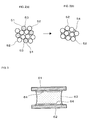
- solder paste including low melting point metal (for example, Sn) balls 51 , high melting point metal (for example, Cu) balls 52 and a flux 53 reacts by heating, and after soldering, as shown in FIG. 2( b ), a plurality of high melting point metal balls 52 are connected to one another with an intermetallic compound 54 , which a low melting point metal derived from the low melting point metal ball forms with a high melting point metal derived from the high melting point metal ball, interposed therebetween, and objects to be joined are connected (soldered) to each other by this connected body.
- intermetallic compound 54 which a low melting point metal derived from the low melting point metal ball forms with a high melting point metal derived from the high melting point metal ball, interposed therebetween, and objects to be joined are connected (soldered) to each other by this connected body.
- an intermetallic compound of the high melting point metal (for example, Cu) and the low melting point metal (for example, Sn) is produced by heating the solder paste in a soldering step, and when a combination of Cu (high melting point metal) and Sn (low melting point metal) is employed, the low melting point metal, Sn, remains since its diffusing rate is low.
- Sn remains, joint strength under an elevated temperature is significantly deteriorated, and there may be cases where a product to be joined cannot be used depending on the type thereof.
- a laminer intermetallic compound 64 such as Cu 3 Sn or Cu 6 Sn 5 is formed at an interface between objects to be joined 61 , 62 after reflow and a joining material (solder) 63 . If such a laminar intermetallic compound 64 is formed, joint strength at the interface is deteriorated through production of cracks or the like because stress is concentrated at the interface.
- the present invention was made to solve the above-mentioned problems, and it is an object of the present invention to provide a joining method, a joint structure, an electronic device, a method for manufacturing an electronic device and an electronic part with which a first metal member can be joined to a second metal member while securing sufficient joint strength, and flow out of a joining material at a second reflow stage in bonding with temperature hierarchy can be inhibited/prevented.
- a joining method of the present invention includes the steps of locating a joining material including a low melting point metal having a lower melting point than a first metal and/or a second metal between a first metal member having at least a surface made of the first metal and a second metal member having at least a surface made of the second metal, and heating the joining material at a temperature equal to or higher than the melting point of the low melting point metal, and is characterized in that in the step of heating the joining material, an intermetallic compound is produced by a reaction of the low melting point metal with the first metal and/or the second metal, and the reaction is repeated while the intermetallic compound is peeled/dispersed in the melted low melting point metal.
- a method for manufacturing an electronic device of the present invention is a method for manufacturing an electronic device including a first metal member having at least a surface made of a first metal and a second metal member having at least a surface made of a second metal, including the step of joining the first metal member to the second metal member by the joining method.
- a joining method of the present invention is a joining method for joining a first metal member having at least a surface made of a first metal to a second metal member having at least a surface made of a second metal with a joining material predominantly made of a low melting point metal having a lower melting point than the first metal and/or the second metal sandwiched between the first metal member and the second metal member, wherein the low melting point metal composing the joining material is Sn or an alloy containing Sn in an amount of 70% by weight or more, at least one of the first metal and the second metal is a metal or an alloy which forms an intermetallic compound with the low melting point metal composing the joining material, and which has a lattice constant difference of 50% or more from the intermetallic compound produced on the surface of at least one of the first metal and the second metal, and the joining method includes a heat treatment step of heat-treating the joining material located between the first metal member and the second metal member at a temperature at which the low melting point metal composing the joining material is melted to join the first
- the low melting point metal is preferably Sn or an alloy containing Sn in an amount of 85% by weight or more.
- the heat treatment step is performed in a state where the proportion of (b) one, of the first metal and the second metal, having the lattice constant difference of 50% or more in the total amount of (a) the low melting point metal composing the joining material and (b) is 30% by volume or more.
- the low melting point metal composing the joining material is Sn alone or an alloy containing Sn and at least one selected from the group consisting of Cu, Ni, Ag, Au, Sb, Zn, Bi, In, Ge, Al, Co, Mn, Fe, Cr, Mg, Mn, Pd, Si, Sr, Te and P.
- At least one of the first metal and the second metal is preferably a Cu—Mn alloy or a Cu—Ni alloy.
- At least one of the first metal and the second metal is preferably a Cu—Mn alloy containing Mn in the proportion of 5 to 30% by weight or a Cu—Ni alloy containing Ni in the proportion of 5 to 30% by weight, and particularly preferably a Cu—Mn alloy containing Mn in the proportion of 10 to 15% by weight or a Cu—Ni alloy containing Ni in the proportion of 10 to 15% by weight.
- a method for manufacturing an electronic device of the present invention is a method for manufacturing an electronic device including a first metal member having at least a surface made of a first metal and a second metal member having at least a surface made of a second metal, including the step of joining the first metal member to the second metal member by the joining method.
- a joint structure of the present invention is a joint structure in which a first metal member is joined to a second metal member with a joint portion sandwiched therebetween, wherein a Cu-M-Sn (M is Ni and/or Mn) intermetallic compound is dispersed in the joint portion, and neither a Cu 3 Sn layer nor a Cu 6 Sn 5 layer, which is an intermetallic compound layer, is formed on at least one of interfaces with the first metal member and the second metal member.
- M is Ni and/or Mn
- the intermetallic compound layer is not formed on both the interface with the first metal member and the interface with the second metal member in the joint portion.
- An electronic device of the present invention is an electronic device in which a first metal member having at least a surface made of a first metal is joined to a second metal member having at least a surface made of a second metal with a joint portion sandwiched therebetween.
- an electronic part of the present invention is an electronic part including an electrode to be subjected to joining by a joining material including a low melting point metal of Sn or an alloy containing Sn in an amount of 70% by weight or more, wherein the surface of the electrode in contact with the joining material is formed of a metal or an alloy which forms an intermetallic compound with the low melting point metal, and which has a lattice constant difference of 50% or more from the intermetallic compound produced on the surface of the electrode by a reaction of the surface of the electrode with the low melting point metal.
- the surface of the electrode in contact with the joining material is preferably formed of a Cu—Mn alloy or a Cu—Ni alloy.
- the Cu—Mn alloy or the Cu—Ni alloy is preferably a Cu—Mn alloy containing Mn in the proportion of 5 to 30% by weight or a Cu—Ni alloy containing Ni in the proportion of 5 to 30% by weight, and moreover preferably a Cu—Mn alloy containing Mn in the proportion of 10 to 15% by weight or a Cu—Ni alloy containing Ni in the proportion of 10 to 15% by weight.
- a joining material including a low melting point metal having a lower melting point than a first metal and/or a second metal is located between a first metal member having at least a surface made of the first metal and a second metal member having at least a surface made of the second metal, and the joining material is heated at a temperature equal to or higher than the melting point of the low melting point metal, and in the step of heating the joining material, by a reaction of the low melting point metal with the first metal and/or the second metal, an intermetallic compound is produced and the reaction is repeated while the intermetallic compound is peeled/dispersed in the melted low melting point metal.
- the interdiffusion between the first metal and/or the second metal and the low melting point metal outstandingly proceeds to promote the conversion to an intermetallic compound having a higher melting point, and therefore it becomes possible to perform joining with large strength in high temperature, adequate joint strength and impact resistance.
- the method for manufacturing an electronic part of the present invention can efficiently manufacture a highly reliable electronic part in which the first metal member is surely joined to the second metal member with the joining material sandwiched therebetween since the method includes the step of joining the first metal member to the second metal member by the joining method.
- the joining method of the present invention it is possible to inhibit/prevent remelting of the joining material also in reflowing a joined body obtained by joining by the method of the present invention secondly, and to improve joint strength and impact resistance since, in joining the first metal member having at least a surface made of a first metal to the second metal member having at least a surface made of a second metal with the joining material predominantly made of a low melting point metal having a lower melting point than the first metal and/or the second metal sandwiched between the first metal member and the second metal member, the low melting point metal composing the joining material is Sn or an alloy containing Sn in an amount of 70% by weight or more, and at least one of the first metal and the second metal is a metal or an alloy which forms an intermetallic compound with the low melting point metal composing the joining material, and which has a lattice constant difference of 50% or more from the intermetallic compound produced on the surface of at least one of the first metal and the second metal.
- the interdiffusion between the first metal and/or the second metal and the low melting point metal outstandingly proceeds to promote the conversion to an intermetallic compound having a higher melting point, and therefore it becomes possible to perform joining with large strength in high temperature, adequate joint strength and impact resistance.
- the “lattice constant difference” is defined as a value (%) determined by subtracting the lattice constant of the first metal or the second metal from the lattice constant of the intermetallic compound of the first metal or the second metal and the low melting point metal and dividing the obtained value by the lattice constant of the first metal or the second metal, followed by multiplying an absolute value of the obtained value by 100.
- the lattice constant difference shows how large a difference there is between the lattice constant of an intermetallic compound newly produced at the interface with the first metal and/or the second metal and the lattice constant of the first metal and/or the second metal, and it does not matter which lattice constant is greater.
- Lattice constant difference (%) ⁇ (Lattice constant of intermetallic compound ⁇ Lattice constant of first metal or second metal)/Lattice constant of first metal or second metal ⁇ 100.
- joining of the first metal member to the second metal member is performed by heat-treating the joining material located between the first metal member and the second metal member at a temperature at which the low melting point metal composing the joining material is melted
- examples of a specific state where such joining (heat-treatment) is performed include 1) a state where the first metal and the second metal are metal materials composing the first metal member (electrode body) and the second metal member (electrode body) to be joined to each other, respectively, at least one of the first metal and the second metal is a metal material having a lattice constant difference of 50% or more from the intermetallic compound, and the low melting point metal is supplied between the first metal member and the second metal member as a solder paste or plate-like solder, and 2) a state where the first metal and the second metal are metal materials composing plating films formed on the surfaces of the first metal member (electrode body) and the second metal member (electrode body) to be joined to each other, respectively
- the heat treatment step when the heat treatment step is performed in a state where the proportion of (b) one, of the first metal and the second metal, having the lattice constant difference of 50% or more in the total amount of (a) the low melting point metal composing the joining material and (b) is 30% by volume or more, since the diffusion of one having the lattice constant difference of 50% or more of the first metal and the second metal into the low melting point material composing the joining material adequately proceeds to promote the conversion to an intermetallic compound having a higher melting point, resulting in a very small amount of remaining low melting point metal component, it becomes possible to perform joining with larger strength in high temperature.
- a “state where the proportion of (b) one, of the first metal and the second metal, having the lattice constant difference of 50% or more . . . is 30% by volume or more” refers to a state represented by the following formula (2), for example, when both of the first metal and the second metal have a lattice constant difference of 50% or more. [(first metal+second metal)/ ⁇ low melting point metal+(first metal+second metal) ⁇ ] ⁇ 100 ⁇ 30(% by volume) (2)
- the low melting point metal composing the joining material is Sn alone or an alloy containing Sn and at least one selected from the group consisting of Cu, Ni, Ag, Au, Sb, Zn, Bi, In, Ge, Al, Co, Mn, Fe, Cr, Mg, Mn, Pd, Si, Sr, Te and P, it is possible that the low melting point metal easily forms an intermetallic compound with at least one of the first metal and the second metal having a lattice constant difference of 50% or more from the low melting point metal.
- the metal forms an intermetallic compound with the low melting point metal at a lower temperature and in a shorter time, and it is possible to prevent the metal from melting also in a subsequent reflow step.
- the metal forms an intermetallic compound more reliably with the low melting point metal at a low temperature and in a shorter time, and the present invention can be made more effective.
- an electronic device including a first metal member having at least a surface made of a first metal and a second metal member having at least a surface made of a second metal, it is possible to manufacture efficiently a highly reliable electronic device in which the first metal member is surely joined to the second metal member with the joining material sandwiched therebetween by joining the first metal member to the second metal member by the above-mentioned joining method.
- the joint structure of the present invention since at least a Cu-M-Sn (M is nickel and/or Mn) intermetallic compound is dispersed in the joint portion where the first metal member is joined to the second metal member and the ratio of an unreacted Sn component not converted to an intermetallic compound to the whole joining material is 30% by weight or less, the joint structure has excellent strength in high temperature to avoid the joining material from remelting and flowing out in the step of second reflow or the like, and can increase joint strength between the first metal member and the second metal member.
- M nickel and/or Mn
- the joint structure of the present invention can provide a highly reliable joint structure in which cracks or the like resulting from the concentration of stress such as thermal stress are hardly produced, and joint strength between the first metal member and the second metal member against thermal shock is large.
- the electronic device of the present invention is an electronic device in which the first metal member having at least a surface made of a first metal is joined to the second metal member having at least a surface made of a second metal with the joint portion sandwiched therebetween, and the joint portion where the first metal member is joined to the second metal member is adapted to have the joint structure.
- the electronic part of the present invention is an electronic part including an electrode to be subjected to joining by a joining material including a low melting point metal of Sn or an alloy containing Sn in an amount of 70% by weight or more, and the surface of the electrode in contact with the joining material is formed of a metal or an alloy which forms an intermetallic compound with the low melting point metal, and which has a lattice constant difference of 50% or more from the intermetallic compound produced on the surface of the electrode by a reaction of the surface of the electrode with the low melting point metal.
- FIGS. 1( a ), 1 ( b ) and 1 ( c ) are drawings schematically showing a behavior in joining by a joining method of an example of the present invention, wherein FIG. 1( a ) is a drawing showing a state before heating, FIG. 1( b ) is a drawing showing a state where heating is initiated and a joining material is melted, and FIG. 1( c ) is a drawing showing a state where heating is continued and an intermetallic compound of a low melting point metal composing the joining material and at least one of a first metal member and a second metal member is formed.
- FIGS. 2( a ) and 2 ( b are drawings showing a behavior of solder in soldering by using a conventional solder paste, wherein FIG. 2( a ) is a view showing a state before heating and FIG. 2( b ) is a view showing a state after the completion of a soldering step.
- FIG. 3 is a drawing showing a joint structure in which a laminar intermetallic compound is formed on an interface in joining by using a conventional solder paste.
- a first metal member 11 a made of a first metal was joined to a second metal member 11 b made of a second metal by using a joining material 10 predominantly made of a low melting point metal having a lower melting point than the first metal and the second metal.
- the low melting point metal composing the joining material as shown in Table 1A and Table 1B, Sn-3Ag-0.5Cu, Sn, Sn-3.5Ag, Sn-0.75Cu, Sn-0.7Cu-0.05Ni, Sn-5Sb, Sn-2Ag-0.5Cu-2Bi, Sn-57Bi-1Ag, Sn-3.5Ag-0.5Bi-8In, Sn-9Zn, Sn-8Zn-3Bi, Sn-10Bi, Sn-20Bi, Sn-30Bi, or Sn-40Bi was used.
- Sn-3Ag-0.5Cu represents an alloy (Sn alloy) in which the low melting point metal material contains Ag in an amount of 3% by weight and Cu in an amount of 0.5% by weight and the rest is Sn. Therefore, Sn-40Bi among the above-mentioned low melting point materials is a material of a comparative example which does not meet the requirement of the present invention that “Sn or an alloy containing Sn in an amount of 70% by weight or more”.
- the first metal member and the second metal member as shown in Table 1A and Table 1B, a metal member made of Cu-10Ni, Cu-10Mn, Cu-12Mn-4Ni, Cu-10Mn-1P, Cu or Cu-10Zn was used.
- a joining material shaped into a plate was located between the first metal member and the second metal member and reflowed at 250° C. for 30 minutes under a load to join the first metal member to the second metal member.
- a joining material 10 shaped into a plate is positioned between a first metal member 11 a and a second metal member 11 b.
- the joining material is reflowed at 250° C. for 15 minutes under a load to melt the low melting point metal (Sn or a Sn alloy) composing the joining material 10 , as shown in FIG. 1( b ). Then, by further keeping on heating for a predetermine time (15 minutes) (that is, by reflowing at 250° C. for 30 minutes), the low melting point metal composing the joining material 10 is melted and reacted with the first metal and/or the second metal respectively composing the first metal member 11 a and the second metal member 11 b to produce an intermetallic compound 12 ( FIG. 1( c )).
- a predetermine time that is, by reflowing at 250° C. for 30 minutes
- the joined bodies thus obtained were used as samples, and their characteristics were measured and evaluated by the following methods.
- Measurement of the shear strength was carried out at a lateral push rate of 0.1 mm/s 1 under conditions of room temperature and 260° C.
- a sample having a shear strength of 20 Nmm ⁇ 2 or more was rated as “ ⁇ ” (excellent), and a sample having a shear strength of 2 Nmm ⁇ 2 or less was rated as “x” (defective).
- the measured joint strength (room temperature, 260° C.) of the samples and the results of evaluation are collectively shown in Table 1A and Table 1B.
- a portion of about 7 mg of the joining material (reaction product) containing an intermetallic compound solidified after the reflow was cut off, and analyzed at a temperature rise rate of 5° C./min at a measurement temperature of 30° C. to 300° C. in a nitrogen atmosphere using Al 2 O 3 as a reference by using differential scanning calorimetry (DSC).
- the amount of the remaining low melting point metal component was quantified from an endothermic quantity of an endothermic melting peak at a melting temperature of the low melting point metal component in the resulting DSC chart and the content (% by volume) of the remaining low melting point metal was determined.
- the obtained joined bodies were sealed with an epoxy resin, left standing in an environment of 85% in relative humidity, and heated in the reflow condition of a peak temperature of 260° C. to determine an incidence rate of flow out defective in which the joining material was remelted and flown out.
- the flow out percent defective was determined from this result and evaluated.
- the obtained joined bodies were subjected to a test in which a cycle of respectively holding a sample for 30 minutes under the temperature conditions of ⁇ 40° C. and +85° C. is repeated a thousand times, and then production of cracks of each sample was observed. Then, the existence or non-existence of production of cracks was evaluated.
- the joint strength of the samples after the thermal shock test was evaluated in the same way as in the above test.
- a sample having a shear strength of 20 Nmm ⁇ 2 or more was rated as “ ⁇ ” (excellent)
- a sample having a shear strength of 10 Nmm ⁇ 2 or more and less than 20 Nmm ⁇ 2 was rated as “ ⁇ ” (good)
- a sample having a shear strength of less than 10 Nmm ⁇ 2 was rated as “x” (defective).
- composition of the low melting point metal composing the joining material
- composition and the lattice constant of metals (a first metal and a second metal) composing the first metal member and the second metal member (in Tables 1A and 1B, the first metal and the second metal are the same metal in the sample Nos. 1 to 15 and different metals in the sample Nos. 16 and 17),
- the lattice constant of an intermetallic compound produced by the reaction of the low melting point metal composing the joining material with the first metal and/or the second metal was evaluated based on a axis
- lattice constant difference which is a difference between the lattice constant of the intermetallic compound and the lattice constant of the first metal and/or the second metal
- a laminar intermetallic compound such as Cu 3 Sn and Cu 6 Sn 5 formed on the interface between the first metal member and/or the second metal member made of a metal having a lattice constant difference of 50% or more from the intermetallic compound and the joint portion (joining material including an intermetallic compound) which is solidified after reflow and joins the first metal member to the second metal member in the joint portion.
- the content of the remaining low melting point metal was larger than 30% by volume, and on the other hand, in all of the samples of examples of sample Nos. 1 to 17, the content of the remaining low melting point metal could be made 30% by volume or less, and particularly in all of the samples of examples of sample Nos. 1 to 9 and 11 to 17 in which Sn or an alloy containing Sn in an amount of 85% by weight or more was used as a low melting point metal, the content of the remaining low melting point metal was 0% by volume.
- the flow out percent defective of the joining material it was found that in the samples of comparative examples of sample Nos. 18 to 20, the flow out percent defective was 70% or more, and on the other hand, in all of the samples of examples of sample Nos. 1 to 17, the flow out percent defective was 20% or less, and particularly all of the samples of examples of sample Nos. 1 to 9 and 11 to 17, in which Sn or an alloy containing Sn in an amount of 85% by weight or more was used as a low melting point metal, had high heat resistance as the flow out percent defective was 0%.
- samples of examples of sample Nos. 1 to 17 which satisfy the requirements of the present invention include:
- the joint strength after the thermal shock test was as low as 5 Nmm ⁇ 2 (sample No. 18), 7 Nmm ⁇ 2 (sample No. 19), or 8 Nmm ⁇ 2 (sample No. 20), but in the samples of sample Nos. 1 to 17 which meet the requirements of the present invention, it was found that the joint strength after the thermal shock test was largely improved compared with that in comparative examples.
- the joint strength after the thermal shock test was 20 Nmm ⁇ 2 or more, that in the sample of sample No. 10 (sample in which the content of Sn in the low melting point metal is 70% by weight), the joint strength after the thermal shock test was 17 Nmm ⁇ 2 , and that in the sample of sample No. 17 (sample in which a first metal member (upper metal member) is Cu and a second metal member (lower metal member) is Cu-10Mn), the joint strength after the thermal shock test was 15 Nmm ⁇ 2 , and these joint strengths were smaller than those of the samples of sample Nos. 1 to 9 and 11 to 16 but were at an adequately practicable level.
- Cu composing the first metal member has a lattice constant difference of less than 50% from an upper intermetallic compound
- Cu-10Mn composing the lower second metal member is a metal having a lattice constant difference of more than 50% from the intermetallic compound, and therefore Cu-10Mn reacts quickly with Sn or a Sn alloy which is a low melting point metal in the joining material.
- a laminar intermetallic compound such as Cu 3 Sn or Cu 6 Sn 5 was not formed on the interface with the second metal member made of a metal (Cu-10Mn) having a lattice constant difference of more than 50% from the intermetallic compound.
- samples of sample Nos. 1 to 17 satisfying the requirements of the present invention have high heat resistance as described above is probably that Cu—Mn and a Cu—Ni alloy respectively having a lattice constant difference of 50% or more from the intermetallic compounds (Cu 2 MnSn and Cu 2 NiSn) which Cu—Mn and Cu—Ni form with the low melting point metal composing the joining material are used for at least one of the first metal and the second metal respectively composing the first metal member and the second metal member.
- Cu—Mn and a Cu—Ni alloy respectively having a lattice constant difference of 50% or more from the intermetallic compounds (Cu 2 MnSn and Cu 2 NiSn) which Cu—Mn and Cu—Ni form with the low melting point metal composing the joining material are used for at least one of the first metal and the second metal respectively composing the first metal member and the second metal member.
- the intermetallic compound produced has a large lattice constant difference from the first metal composing the first metal member and/or the second metal composing the second metal member, since the reaction is repeated while the intermetallic compound is peeled/dispersed in the melted low melting point metal, it is thought that the production rate of the intermetallic compound outstandingly increases and the laminar intermetallic compound is not formed at the interface.
- a joining material using Sn as a low melting point metal was used, and a first metal member and a second metal member, respectively made of Cu-10Ni, were joined to each other (samples of sample Nos. 21 to 27 in Table 2).
- Thicknesses of the first metal member and the second metal member were set to 0.1 mm.
- the first metal member was joined to the second metal member under the same conditions as in Example 1 except for the above-mentioned thicknesses.
- Example 2 a sample having a shear strength of 20 Nmm ⁇ 2 or more was rated as “ ⁇ ” (excellent), a sample having a shear strength of 2 Nmm ⁇ 2 or more and less than 20 Nmm ⁇ 2 was rated as “ ⁇ ” (good), and a sample having a shear strength of less than 2 Nmm ⁇ 2 was rated as “x” (defective).
- the joint strength (room temperature, 260° C.), the content of the remaining low melting point metal, the flow out percent defective and the existence or non-existence of cracks and joint strength after a thermal shock test of the joined bodies are shown in Table 2.
- each of samples of sample Nos. 21 to 30 has a joint strength of 7 to 26 Nmm ⁇ 2 that is 2 Nmm ⁇ 2 or more, and it was found that practicable joining was performed.
- the samples of sample Nos. 21 to 23, 28 and 29, in which the proportion of Cu-10Mn was 30% by volume or more exhibited a joint strength of 23 Nmm ⁇ 2 or more, and were found to have high strength in high temperature.
- a first metal member and a second metal member were joined to each other by using a joining material using Sn as a low melting point metal.
- a first metal member and a second metal member were joined to each other by using a joining material using Sn as a low melting point metal.
- Thicknesses of the first metal member and the second metal member were set to 0.3 mm.
- the joining material a plate-like joining material having a thickness of 0.1 mm was used.
- the first metal member was joined to the second metal member under the same conditions as in Example 1 except for the above-mentioned thicknesses.
- the joint strength (room temperature, 260° C.), the content of the remaining low melting point metal, the flow out percent defective and the existence or non-existence of cracks and joint strength after a thermal shock test of the joined bodies are shown in Table 3.
- each of samples of sample Nos. 31 to 39 was found to have a joint strength of 5 to 26 Nmm ⁇ 2 which is a practicable joint strength of 2 Nmm ⁇ 2 or more.
- the samples of sample No. 32 in which the first metal and the second metal were Cu-10Mn, the sample of sample No. 33 in which the first metal and the second metal were Cu-15Mn, the sample of sample No. 37 in which the first metal and the second metal were Cu-10Ni, and the sample of sample No. 38 in which the first metal and the second metal were Cu-15Ni exhibited a joint strength of 24 Nmm ⁇ 2 or more, and were found to have high strength in high temperature.
- the content of the remaining low melting point metal it was found that all of the samples of sample Nos. 31 to 39 exhibited a content of the remaining low melting point metal of 30% by volume or less, and moreover in the sample of sample No. 32 in which the first metal and the second metal were Cu-10Mn, the sample of sample No. 33 in which the first metal and the second metal were Cu-15Mn, the sample of sample No. 37 in which the first metal and the second metal were Cu-10Ni and the sample of sample No. 38 in which the first metal and the second metal were Cu-15Ni, the content of the remaining low melting point metal was 0% by volume.
- the plate-like joining material was used as a joining material containing a low melting point metal, but in Example 4, a solder paste obtained by mixing a flux and a low melting point metal (Sn-3Ag-0.5Cu powder) was used, and a first metal member made of Cu and a second metal member made of Cu-10Mn were joined to each other.
- a solder paste obtained by mixing a flux and a low melting point metal Sn-3Ag-0.5Cu powder
- solder paste was printed on the first metal member made of Cu, and the second metal member made of Cu-10Mn was overlaid thereon, and then reflowing was performed at 250° C. for 30 minutes to join the first metal member to the second metal member.
- the present invention has been described taking a case where the whole first metal member is made of the first metal and the whole second metal member is made of the second metal as an example, but it is also possible to employ a constitution in which the first metal and the second metal are metal materials composing plating films formed on the surfaces of the first metal member (electrode body) and the second metal member (electrode body) to be joined to each other, respectively, and at least one of the first metal and the second metal is a metal material having a lattice constant difference of 50% or more from the intermetallic compound.
- Example 5 a solder paste obtained by mixing a flux and a low melting point metal (Sn-3Ag-0.5Cu powder) was used, and an electronic device having a structure in which a chip capacitor and a surface acoustic wave filter were mounted on a glass epoxy board was manufactured by joining a land electrode (first metal member in the present invention) made of Cu on the glass epoxy board to an external electrode (second metal member in the present invention) made of Cu-10Mn of the chip capacitor (electronic part) and the surface acoustic wave filter (SAW filter) (electronic part).
- a land electrode first metal member in the present invention
- second metal member in the present invention an external electrode
- SAW filter surface acoustic wave filter
- the electronic device is an electronic device having a structure in which the above first metal member is joined to the above second metal member with a joining material meeting the requirements of the present invention sandwiched therebetween.
- the above-mentioned solder paste was printed on the first metal member made of Cu of a glass epoxy board, and the external electrode (second metal member) made of Cu-10Mn of the chip capacitor and a SAW filter was overlaid thereon, and then reflowing was performed at 250° C. for 30 minutes to join the first metal member to the second metal member.
- the thickness of the first metal member was set to 0.05 mm and the thickness of the second metal member was set to 0.05 mm.
- solder paste was printed on the land electrode by using a metal mask having a thickness of 0.05 mm.
- Characteristics of the resulting joined bodies were measured and evaluated in the same way as in Example 1. Specifically, measurement of joint strength, evaluation of the remaining component, evaluation of flow out, and evaluation of existence or non-existence of cracks and measurement of joint strength after a thermal shock test were performed, and characteristics were evaluated.
- the joint strength (room temperature, 260° C.), the content of the remaining low melting point metal, the flow out percent defective and the existence or non-existence of cracks and joint strength after a thermal shock test of the joined bodies are shown in Table 4.
- Example 5 As shown in Table 4, it was found that also in Example 5, a joined body having characteristics equal to those of samples of Examples 1 to 4 which meet the requirements of the present invention was obtained.
- first metal and the second metal are metal materials composing plating films formed on the surfaces of the first metal member (electrode body) and the second metal member (electrode body) to be joined to each other, respectively, and at least one of the first metal and the second metal is a metal material having a lattice constant difference of 50% or more from the intermetallic compound.
- the present invention is not intended to be limited to the above-mentioned examples, and various applications and variations may be made within the scope of the invention regarding types and composition of the low melting point metal composing the joining material, and types and composition of materials composing the first metal member having at least a surface made of a first metal and the second metal member having at least a surface made of a second metal.
Landscapes
- Engineering & Computer Science (AREA)
- Mechanical Engineering (AREA)
- Chemical & Material Sciences (AREA)
- Materials Engineering (AREA)
- Metallurgy (AREA)
- Organic Chemistry (AREA)
- Manufacturing & Machinery (AREA)
- Microelectronics & Electronic Packaging (AREA)
- Electric Connection Of Electric Components To Printed Circuits (AREA)
- Pressure Welding/Diffusion-Bonding (AREA)
- Die Bonding (AREA)
Priority Applications (1)
| Application Number | Priority Date | Filing Date | Title |
|---|---|---|---|
| US14/918,648 US9614295B2 (en) | 2010-12-24 | 2015-10-21 | Joining method, joint structure, electronic device, method for manufacturing electronic device and electronic part |
Applications Claiming Priority (5)
| Application Number | Priority Date | Filing Date | Title |
|---|---|---|---|
| JP2010-287782 | 2010-12-24 | ||
| JP2010287782 | 2010-12-24 | ||
| JP2011-159922 | 2011-07-21 | ||
| JP2011159922 | 2011-07-21 | ||
| PCT/JP2011/079781 WO2012086745A1 (ja) | 2010-12-24 | 2011-12-22 | 接合方法、接合構造、電子装置、電子装置の製造方法、および電子部品 |
Related Parent Applications (1)
| Application Number | Title | Priority Date | Filing Date |
|---|---|---|---|
| PCT/JP2011/079781 Continuation WO2012086745A1 (ja) | 2010-12-24 | 2011-12-22 | 接合方法、接合構造、電子装置、電子装置の製造方法、および電子部品 |
Related Child Applications (1)
| Application Number | Title | Priority Date | Filing Date |
|---|---|---|---|
| US14/918,648 Division US9614295B2 (en) | 2010-12-24 | 2015-10-21 | Joining method, joint structure, electronic device, method for manufacturing electronic device and electronic part |
Publications (2)
| Publication Number | Publication Date |
|---|---|
| US20130299236A1 US20130299236A1 (en) | 2013-11-14 |
| US9209527B2 true US9209527B2 (en) | 2015-12-08 |
Family
ID=46314012
Family Applications (2)
| Application Number | Title | Priority Date | Filing Date |
|---|---|---|---|
| US13/904,072 Active 2032-07-26 US9209527B2 (en) | 2010-12-24 | 2013-05-29 | Joining method, joint structure, electronic device, method for manufacturing electronic device and electronic part |
| US14/918,648 Active US9614295B2 (en) | 2010-12-24 | 2015-10-21 | Joining method, joint structure, electronic device, method for manufacturing electronic device and electronic part |
Family Applications After (1)
| Application Number | Title | Priority Date | Filing Date |
|---|---|---|---|
| US14/918,648 Active US9614295B2 (en) | 2010-12-24 | 2015-10-21 | Joining method, joint structure, electronic device, method for manufacturing electronic device and electronic part |
Country Status (7)
| Country | Link |
|---|---|
| US (2) | US9209527B2 (enExample) |
| EP (1) | EP2656955B1 (enExample) |
| JP (2) | JP5664664B2 (enExample) |
| KR (1) | KR101528515B1 (enExample) |
| CN (1) | CN103167926B (enExample) |
| TW (1) | TWI461252B (enExample) |
| WO (1) | WO2012086745A1 (enExample) |
Cited By (1)
| Publication number | Priority date | Publication date | Assignee | Title |
|---|---|---|---|---|
| US10751841B2 (en) | 2016-02-01 | 2020-08-25 | Murata Manufacturing Co., Ltd. | Bonding material, and bonding method and bonded structure each using same |
Families Citing this family (22)
| Publication number | Priority date | Publication date | Assignee | Title |
|---|---|---|---|---|
| CN105873713B (zh) * | 2014-01-07 | 2018-07-10 | 株式会社村田制作所 | 结构材料接合方法、接合用片材和接合结构 |
| JP6213666B2 (ja) * | 2014-04-18 | 2017-10-18 | 株式会社村田製作所 | 被着体の接着分離方法 |
| JP6287739B2 (ja) * | 2014-09-30 | 2018-03-07 | 株式会社村田製作所 | ステンドグラスの製造方法 |
| CN105081500B (zh) * | 2015-09-02 | 2017-02-22 | 哈尔滨工业大学 | 一种使用激光前向转印具有特定晶粒取向和数量薄膜诱发金属间化合物生长的方法 |
| JP6332566B2 (ja) | 2015-09-15 | 2018-05-30 | 株式会社村田製作所 | 接合用部材、接合用部材の製造方法、および、接合方法 |
| JP6528852B2 (ja) | 2015-09-28 | 2019-06-12 | 株式会社村田製作所 | ヒートパイプ、放熱部品、ヒートパイプの製造方法 |
| WO2017077824A1 (ja) * | 2015-11-05 | 2017-05-11 | 株式会社村田製作所 | 接合用部材、および、接合用部材の製造方法 |
| JP6621068B2 (ja) * | 2016-12-08 | 2019-12-18 | パナソニックIpマネジメント株式会社 | 実装構造体 |
| JP6355091B1 (ja) * | 2017-03-07 | 2018-07-11 | パナソニックIpマネジメント株式会社 | はんだ合金およびそれを用いた接合構造体 |
| WO2018174066A1 (ja) * | 2017-03-23 | 2018-09-27 | 積水化学工業株式会社 | 導電性粒子、導電材料及び接続構造体 |
| DE102017206932A1 (de) * | 2017-04-25 | 2018-10-25 | Siemens Aktiengesellschaft | Lotformteil zum Erzeugen einer Diffusionslötverbindung und Verfahren zum Erzeugen eines Lotformteils |
| JP6998557B2 (ja) * | 2017-09-29 | 2022-01-18 | パナソニックIpマネジメント株式会社 | はんだ合金およびそれを用いた接合構造体 |
| CN108098172B (zh) * | 2017-12-01 | 2020-03-27 | 北京工业大学 | 一种实现Cu/Sn/Cu界面可逆连接的方法 |
| KR102574413B1 (ko) * | 2018-12-10 | 2023-09-04 | 삼성전기주식회사 | 코일 전자 부품 |
| US11581239B2 (en) * | 2019-01-18 | 2023-02-14 | Indium Corporation | Lead-free solder paste as thermal interface material |
| KR102148297B1 (ko) * | 2019-03-06 | 2020-08-26 | 성균관대학교산학협력단 | 이종 금속 재료 간의 접합을 위한 천이액상소결접합 방법 |
| CN109822256B (zh) * | 2019-03-15 | 2021-08-06 | 南昌大学 | 一种低熔点In-Sn-Bi合金钎料及制备方法 |
| CN114173983A (zh) * | 2019-07-26 | 2022-03-11 | 日本斯倍利亚社股份有限公司 | 预制焊料和使用该预制焊料形成的焊料接合体 |
| DE112020004146T5 (de) * | 2019-09-02 | 2022-05-25 | Nihon Superior Co., Ltd. | Lötpasten und lötstellen |
| CN113275787B (zh) * | 2020-01-31 | 2023-05-30 | 铟泰公司 | 作为热界面材料的无铅焊料膏 |
| WO2021177006A1 (ja) * | 2020-03-06 | 2021-09-10 | 三菱電機株式会社 | 薄板状接合部材およびその製造方法、半導体装置およびその製造方法、ならびに、電力変換装置 |
| JP6799701B1 (ja) * | 2020-03-12 | 2020-12-16 | 有限会社 ナプラ | 金属粒子 |
Citations (15)
| Publication number | Priority date | Publication date | Assignee | Title |
|---|---|---|---|---|
| JP2002254194A (ja) | 2000-06-12 | 2002-09-10 | Hitachi Ltd | 電子機器およびはんだ |
| JP2002254195A (ja) | 2000-12-25 | 2002-09-10 | Tdk Corp | はんだ付け用組成物及びはんだ付け方法 |
| JP2003094193A (ja) | 2002-06-18 | 2003-04-02 | Matsushita Electric Ind Co Ltd | 鉛フリー半田ペースト |
| JP2003211289A (ja) | 2002-01-21 | 2003-07-29 | Fujitsu Ltd | 導電性接合材料、それを用いた接合方法及び電子機器 |
| US6602777B1 (en) | 2001-12-28 | 2003-08-05 | National Central University | Method for controlling the formation of intermetallic compounds in solder joints |
| JP2003332731A (ja) | 2002-05-09 | 2003-11-21 | Murata Mfg Co Ltd | Pbフリー半田付け物品 |
| US20050212133A1 (en) | 2004-03-29 | 2005-09-29 | Barnak John P | Under bump metallization layer to enable use of high tin content solder bumps |
| US20050218525A1 (en) | 2004-03-31 | 2005-10-06 | Kabushiki Kaisha Toshiba | Soldered material, semiconductor device, method of soldering, and method of manufacturing semiconductor device |
| WO2006075459A1 (ja) | 2005-01-11 | 2006-07-20 | Murata Manufacturing Co., Ltd | はんだペースト、及び電子装置 |
| US20060186550A1 (en) | 2005-02-24 | 2006-08-24 | Osamu Ikeda | Semiconductor device and manufacturing method thereof |
| WO2007125861A1 (ja) | 2006-04-26 | 2007-11-08 | Senju Metal Industry Co., Ltd. | ソルダペースト |
| WO2009051181A1 (ja) | 2007-10-19 | 2009-04-23 | Nihon Superior Sha Co., Ltd. | 無鉛はんだ合金 |
| US20090148720A1 (en) | 2006-09-01 | 2009-06-11 | Murata Manufacturing Co., Ltd. | Electronic component device, method for manufacturing electronic component device, electronic component assembly, and method for manufacturing electronic component assembly |
| CN101681888A (zh) | 2007-06-04 | 2010-03-24 | 株式会社村田制作所 | 电子零部件装置及其制造方法 |
| JP2010149185A (ja) | 2008-11-28 | 2010-07-08 | Asahi Kasei E-Materials Corp | 金属フィラー、はんだペースト、及び接続構造体 |
Family Cites Families (10)
| Publication number | Priority date | Publication date | Assignee | Title |
|---|---|---|---|---|
| US6371361B1 (en) * | 1996-02-09 | 2002-04-16 | Matsushita Electric Industrial Co., Ltd. | Soldering alloy, cream solder and soldering method |
| US5863493A (en) * | 1996-12-16 | 1999-01-26 | Ford Motor Company | Lead-free solder compositions |
| ES2224609T3 (es) * | 1998-03-26 | 2005-03-01 | Nihon Superior Sha Co., Ltd | Aleacion de soldadura exenta de plomo. |
| JP4271684B2 (ja) * | 2003-10-24 | 2009-06-03 | 日鉱金属株式会社 | ニッケル合金スパッタリングターゲット及びニッケル合金薄膜 |
| JP4501818B2 (ja) * | 2005-09-02 | 2010-07-14 | 日立電線株式会社 | 銅合金材およびその製造方法 |
| KR101406174B1 (ko) * | 2007-06-18 | 2014-06-12 | 엠케이전자 주식회사 | 주석, 은 및 비스무스를 함유하는 무연솔더 |
| CN101842506B (zh) * | 2007-11-01 | 2012-08-22 | 古河电气工业株式会社 | 强度、弯曲加工性、抗应力松弛性能优异的铜合金材料及其制造方法 |
| JP5169354B2 (ja) * | 2008-03-18 | 2013-03-27 | 富士通株式会社 | 接合材料及びそれを用いた接合方法 |
| WO2011027659A1 (ja) * | 2009-09-03 | 2011-03-10 | 株式会社村田製作所 | ソルダペースト、それを用いた接合方法、および接合構造 |
| EP2641689B1 (en) * | 2010-11-19 | 2016-06-29 | Murata Manufacturing Co., Ltd. | Electroconductive material, method of connection with same, and connected structure |
-
2011
- 2011-12-21 TW TW100147807A patent/TWI461252B/zh active
- 2011-12-22 EP EP11851801.8A patent/EP2656955B1/en active Active
- 2011-12-22 KR KR1020137007337A patent/KR101528515B1/ko active Active
- 2011-12-22 JP JP2012549868A patent/JP5664664B2/ja active Active
- 2011-12-22 WO PCT/JP2011/079781 patent/WO2012086745A1/ja not_active Ceased
- 2011-12-22 CN CN201180049028.9A patent/CN103167926B/zh active Active
-
2013
- 2013-05-29 US US13/904,072 patent/US9209527B2/en active Active
-
2014
- 2014-06-24 JP JP2014129244A patent/JP5907215B2/ja active Active
-
2015
- 2015-10-21 US US14/918,648 patent/US9614295B2/en active Active
Patent Citations (27)
| Publication number | Priority date | Publication date | Assignee | Title |
|---|---|---|---|---|
| JP2002254194A (ja) | 2000-06-12 | 2002-09-10 | Hitachi Ltd | 電子機器およびはんだ |
| JP2002254195A (ja) | 2000-12-25 | 2002-09-10 | Tdk Corp | はんだ付け用組成物及びはんだ付け方法 |
| US6602777B1 (en) | 2001-12-28 | 2003-08-05 | National Central University | Method for controlling the formation of intermetallic compounds in solder joints |
| JP2003211289A (ja) | 2002-01-21 | 2003-07-29 | Fujitsu Ltd | 導電性接合材料、それを用いた接合方法及び電子機器 |
| JP2003332731A (ja) | 2002-05-09 | 2003-11-21 | Murata Mfg Co Ltd | Pbフリー半田付け物品 |
| JP2003094193A (ja) | 2002-06-18 | 2003-04-02 | Matsushita Electric Ind Co Ltd | 鉛フリー半田ペースト |
| CN1930672A (zh) | 2004-03-29 | 2007-03-14 | 英特尔公司 | 允许使用高含锡量焊块的凸块下金属化层 |
| US20050212133A1 (en) | 2004-03-29 | 2005-09-29 | Barnak John P | Under bump metallization layer to enable use of high tin content solder bumps |
| US7064446B2 (en) | 2004-03-29 | 2006-06-20 | Intel Corporation | Under bump metallization layer to enable use of high tin content solder bumps |
| TWI287264B (en) | 2004-03-29 | 2007-09-21 | Intel Corp | Under bump metallization layer to enable use of high tin content solder bumps |
| US20050218525A1 (en) | 2004-03-31 | 2005-10-06 | Kabushiki Kaisha Toshiba | Soldered material, semiconductor device, method of soldering, and method of manufacturing semiconductor device |
| JP2005288458A (ja) | 2004-03-31 | 2005-10-20 | Toshiba Corp | 接合体、半導体装置、接合方法、及び半導体装置の製造方法 |
| CN101087673A (zh) | 2005-01-11 | 2007-12-12 | 株式会社村田制作所 | 焊膏及电子装置 |
| US20070245852A1 (en) | 2005-01-11 | 2007-10-25 | Murata Manufacturing Co., Ltd. | Solder paste and electronic device |
| WO2006075459A1 (ja) | 2005-01-11 | 2006-07-20 | Murata Manufacturing Co., Ltd | はんだペースト、及び電子装置 |
| US20060186550A1 (en) | 2005-02-24 | 2006-08-24 | Osamu Ikeda | Semiconductor device and manufacturing method thereof |
| US7274103B2 (en) | 2005-02-24 | 2007-09-25 | Renesas Technology Corp. | Semiconductor device and manufacturing method thereof |
| CN1825578A (zh) | 2005-02-24 | 2006-08-30 | 株式会社瑞萨科技 | 半导体器件及其制造方法 |
| WO2007125861A1 (ja) | 2006-04-26 | 2007-11-08 | Senju Metal Industry Co., Ltd. | ソルダペースト |
| CN101512761A (zh) | 2006-09-01 | 2009-08-19 | 株式会社村田制作所 | 电子部件装置及其制造方法与电子部件组件及其制造方法 |
| US20090148720A1 (en) | 2006-09-01 | 2009-06-11 | Murata Manufacturing Co., Ltd. | Electronic component device, method for manufacturing electronic component device, electronic component assembly, and method for manufacturing electronic component assembly |
| CN101681888A (zh) | 2007-06-04 | 2010-03-24 | 株式会社村田制作所 | 电子零部件装置及其制造方法 |
| US20110268977A1 (en) | 2007-06-04 | 2011-11-03 | Murata Manufacturing Co., Ltd. | Electronic component device and method for producing the same |
| US8794498B2 (en) | 2007-06-04 | 2014-08-05 | Murata Manufacturing Co., Ltd. | Electronic component device and method for producing the same |
| WO2009051181A1 (ja) | 2007-10-19 | 2009-04-23 | Nihon Superior Sha Co., Ltd. | 無鉛はんだ合金 |
| US20100266870A1 (en) | 2007-10-19 | 2010-10-21 | Nihon Superior Sha Co., Ltd. | Solder joint |
| JP2010149185A (ja) | 2008-11-28 | 2010-07-08 | Asahi Kasei E-Materials Corp | 金属フィラー、はんだペースト、及び接続構造体 |
Non-Patent Citations (1)
| Title |
|---|
| PCT/JP2011/079781 Written Opinion dated Mar. 27, 2012. |
Cited By (1)
| Publication number | Priority date | Publication date | Assignee | Title |
|---|---|---|---|---|
| US10751841B2 (en) | 2016-02-01 | 2020-08-25 | Murata Manufacturing Co., Ltd. | Bonding material, and bonding method and bonded structure each using same |
Also Published As
| Publication number | Publication date |
|---|---|
| JP5907215B2 (ja) | 2016-04-26 |
| EP2656955A1 (en) | 2013-10-30 |
| US20160043480A1 (en) | 2016-02-11 |
| EP2656955B1 (en) | 2021-08-04 |
| TWI461252B (zh) | 2014-11-21 |
| US9614295B2 (en) | 2017-04-04 |
| CN103167926A (zh) | 2013-06-19 |
| CN103167926B (zh) | 2016-03-09 |
| KR101528515B1 (ko) | 2015-06-12 |
| KR20130077873A (ko) | 2013-07-09 |
| JPWO2012086745A1 (ja) | 2014-06-05 |
| US20130299236A1 (en) | 2013-11-14 |
| JP5664664B2 (ja) | 2015-02-04 |
| WO2012086745A1 (ja) | 2012-06-28 |
| JP2014223678A (ja) | 2014-12-04 |
| TW201233485A (en) | 2012-08-16 |
| EP2656955A4 (en) | 2017-07-19 |
Similar Documents
| Publication | Publication Date | Title |
|---|---|---|
| US9209527B2 (en) | Joining method, joint structure, electronic device, method for manufacturing electronic device and electronic part | |
| US9409247B2 (en) | Joining method, method for producing electronic device and electronic part | |
| US11411150B2 (en) | Advanced solder alloys for electronic interconnects | |
| JP5045673B2 (ja) | 機能部品用リッドとその製造方法 | |
| US10322471B2 (en) | Low temperature high reliability alloy for solder hierarchy | |
| US9333593B2 (en) | Joining method, joint structure and method for producing the same | |
| JP2014223678A5 (enExample) | ||
| US20140193650A1 (en) | Electroconductive material, and connection method and connection structure using the same | |
| US20140178703A1 (en) | Electroconductive material, and connection method and connection structure using the same | |
| WO2010122764A1 (ja) | はんだ材料および電子部品接合体 | |
| US20140356055A1 (en) | Joining method, joint structure and method for producing the same | |
| CN100509257C (zh) | 一种无铅焊球用于生产焊锡凸起的用途以及焊锡凸起 | |
| CN115461188B (zh) | 用于高温应用的具有混合焊料粉末的无铅焊膏 | |
| JP2012206142A (ja) | 半田及び半田を用いた半導体装置並びに半田付け方法 | |
| JP5231727B2 (ja) | 接合方法 | |
| JP6724979B2 (ja) | 接合体 | |
| WO2016157971A1 (ja) | はんだペースト |
Legal Events
| Date | Code | Title | Description |
|---|---|---|---|
| AS | Assignment |
Owner name: MURATA MANUFACTURING CO., LTD., JAPAN Free format text: ASSIGNMENT OF ASSIGNORS INTEREST;ASSIGNORS:NAKANO, KOSUKE;TAKAOKA, HIDEKIYO;REEL/FRAME:030510/0350 Effective date: 20130410 |
|
| STCF | Information on status: patent grant |
Free format text: PATENTED CASE |
|
| MAFP | Maintenance fee payment |
Free format text: PAYMENT OF MAINTENANCE FEE, 4TH YEAR, LARGE ENTITY (ORIGINAL EVENT CODE: M1551); ENTITY STATUS OF PATENT OWNER: LARGE ENTITY Year of fee payment: 4 |
|
| MAFP | Maintenance fee payment |
Free format text: PAYMENT OF MAINTENANCE FEE, 8TH YEAR, LARGE ENTITY (ORIGINAL EVENT CODE: M1552); ENTITY STATUS OF PATENT OWNER: LARGE ENTITY Year of fee payment: 8 |