US8921999B2 - Semiconductor device, semiconductor device manufacturing method, semiconductor device mounting structure and power semiconductor device - Google Patents
Semiconductor device, semiconductor device manufacturing method, semiconductor device mounting structure and power semiconductor device Download PDFInfo
- Publication number
- US8921999B2 US8921999B2 US13/606,581 US201213606581A US8921999B2 US 8921999 B2 US8921999 B2 US 8921999B2 US 201213606581 A US201213606581 A US 201213606581A US 8921999 B2 US8921999 B2 US 8921999B2
- Authority
- US
- United States
- Prior art keywords
- die pad
- heat radiation
- semiconductor device
- resin
- encapsulation portion
- Prior art date
- Legal status (The legal status is an assumption and is not a legal conclusion. Google has not performed a legal analysis and makes no representation as to the accuracy of the status listed.)
- Active, expires
Links
- 239000004065 semiconductor Substances 0.000 title claims abstract description 575
- 238000004519 manufacturing process Methods 0.000 title description 76
- 229920005989 resin Polymers 0.000 claims abstract description 579
- 239000011347 resin Substances 0.000 claims abstract description 579
- 230000005855 radiation Effects 0.000 claims abstract description 356
- 238000005538 encapsulation Methods 0.000 claims abstract description 315
- 239000000758 substrate Substances 0.000 claims description 59
- 230000001788 irregular Effects 0.000 claims description 16
- 230000000994 depressogenic effect Effects 0.000 claims description 5
- 239000010410 layer Substances 0.000 description 184
- 238000000034 method Methods 0.000 description 84
- 239000000463 material Substances 0.000 description 80
- 239000000945 filler Substances 0.000 description 67
- 238000005422 blasting Methods 0.000 description 34
- 239000004020 conductor Substances 0.000 description 21
- 238000005304 joining Methods 0.000 description 19
- 239000011810 insulating material Substances 0.000 description 17
- 229910000679 solder Inorganic materials 0.000 description 15
- VYPSYNLAJGMNEJ-UHFFFAOYSA-N Silicium dioxide Chemical compound O=[Si]=O VYPSYNLAJGMNEJ-UHFFFAOYSA-N 0.000 description 14
- 238000005452 bending Methods 0.000 description 14
- 125000006850 spacer group Chemical group 0.000 description 13
- 230000000694 effects Effects 0.000 description 12
- 239000013528 metallic particle Substances 0.000 description 12
- 230000002265 prevention Effects 0.000 description 10
- 238000004299 exfoliation Methods 0.000 description 9
- 230000017525 heat dissipation Effects 0.000 description 9
- 230000015572 biosynthetic process Effects 0.000 description 8
- 239000000919 ceramic Substances 0.000 description 8
- 229910052782 aluminium Inorganic materials 0.000 description 7
- XAGFODPZIPBFFR-UHFFFAOYSA-N aluminium Chemical compound [Al] XAGFODPZIPBFFR-UHFFFAOYSA-N 0.000 description 7
- PNEYBMLMFCGWSK-UHFFFAOYSA-N aluminium oxide Inorganic materials [O-2].[O-2].[O-2].[Al+3].[Al+3] PNEYBMLMFCGWSK-UHFFFAOYSA-N 0.000 description 7
- 239000000377 silicon dioxide Substances 0.000 description 7
- RYGMFSIKBFXOCR-UHFFFAOYSA-N Copper Chemical compound [Cu] RYGMFSIKBFXOCR-UHFFFAOYSA-N 0.000 description 6
- XEEYBQQBJWHFJM-UHFFFAOYSA-N Iron Chemical compound [Fe] XEEYBQQBJWHFJM-UHFFFAOYSA-N 0.000 description 6
- 229910052802 copper Inorganic materials 0.000 description 6
- 239000010949 copper Substances 0.000 description 6
- 235000012239 silicon dioxide Nutrition 0.000 description 5
- 229910052581 Si3N4 Inorganic materials 0.000 description 4
- 239000000853 adhesive Substances 0.000 description 4
- PMHQVHHXPFUNSP-UHFFFAOYSA-M copper(1+);methylsulfanylmethane;bromide Chemical compound Br[Cu].CSC PMHQVHHXPFUNSP-UHFFFAOYSA-M 0.000 description 4
- 239000004519 grease Substances 0.000 description 4
- HQVNEWCFYHHQES-UHFFFAOYSA-N silicon nitride Chemical compound N12[Si]34N5[Si]62N3[Si]51N64 HQVNEWCFYHHQES-UHFFFAOYSA-N 0.000 description 4
- 229910052582 BN Inorganic materials 0.000 description 3
- PZNSFCLAULLKQX-UHFFFAOYSA-N Boron nitride Chemical compound N#B PZNSFCLAULLKQX-UHFFFAOYSA-N 0.000 description 3
- 229910000881 Cu alloy Inorganic materials 0.000 description 3
- BQCADISMDOOEFD-UHFFFAOYSA-N Silver Chemical compound [Ag] BQCADISMDOOEFD-UHFFFAOYSA-N 0.000 description 3
- 239000003990 capacitor Substances 0.000 description 3
- 230000002708 enhancing effect Effects 0.000 description 3
- 210000003608 fece Anatomy 0.000 description 3
- 229910052742 iron Inorganic materials 0.000 description 3
- 229910052751 metal Inorganic materials 0.000 description 3
- 239000002184 metal Substances 0.000 description 3
- 229910052709 silver Inorganic materials 0.000 description 3
- 239000004332 silver Substances 0.000 description 3
- 229920001187 thermosetting polymer Polymers 0.000 description 3
- 239000012790 adhesive layer Substances 0.000 description 2
- 230000008901 benefit Effects 0.000 description 2
- 239000002131 composite material Substances 0.000 description 2
- 239000003822 epoxy resin Substances 0.000 description 2
- 230000001965 increasing effect Effects 0.000 description 2
- 230000002093 peripheral effect Effects 0.000 description 2
- 229920000647 polyepoxide Polymers 0.000 description 2
- 238000004382 potting Methods 0.000 description 2
- 238000007788 roughening Methods 0.000 description 2
- 238000004544 sputter deposition Methods 0.000 description 2
- 229920005992 thermoplastic resin Polymers 0.000 description 2
- 238000001721 transfer moulding Methods 0.000 description 2
- 239000004593 Epoxy Substances 0.000 description 1
- 230000005489 elastic deformation Effects 0.000 description 1
- 230000005611 electricity Effects 0.000 description 1
- 239000006260 foam Substances 0.000 description 1
- 238000002844 melting Methods 0.000 description 1
- 230000008018 melting Effects 0.000 description 1
- 238000012986 modification Methods 0.000 description 1
- 230000004048 modification Effects 0.000 description 1
- 238000000465 moulding Methods 0.000 description 1
- 238000010298 pulverizing process Methods 0.000 description 1
- 229920002379 silicone rubber Polymers 0.000 description 1
- 238000006467 substitution reaction Methods 0.000 description 1
Images


Classifications
-
- H—ELECTRICITY
- H01—ELECTRIC ELEMENTS
- H01L—SEMICONDUCTOR DEVICES NOT COVERED BY CLASS H10
- H01L23/00—Details of semiconductor or other solid state devices
- H01L23/48—Arrangements for conducting electric current to or from the solid state body in operation, e.g. leads, terminal arrangements ; Selection of materials therefor
- H01L23/488—Arrangements for conducting electric current to or from the solid state body in operation, e.g. leads, terminal arrangements ; Selection of materials therefor consisting of soldered or bonded constructions
- H01L23/495—Lead-frames or other flat leads
- H01L23/49575—Assemblies of semiconductor devices on lead frames
-
- H—ELECTRICITY
- H01—ELECTRIC ELEMENTS
- H01L—SEMICONDUCTOR DEVICES NOT COVERED BY CLASS H10
- H01L21/00—Processes or apparatus adapted for the manufacture or treatment of semiconductor or solid state devices or of parts thereof
- H01L21/02—Manufacture or treatment of semiconductor devices or of parts thereof
- H01L21/04—Manufacture or treatment of semiconductor devices or of parts thereof the devices having potential barriers, e.g. a PN junction, depletion layer or carrier concentration layer
- H01L21/48—Manufacture or treatment of parts, e.g. containers, prior to assembly of the devices, using processes not provided for in a single one of the subgroups H01L21/06 - H01L21/326
- H01L21/4814—Conductive parts
- H01L21/4846—Leads on or in insulating or insulated substrates, e.g. metallisation
- H01L21/4853—Connection or disconnection of other leads to or from a metallisation, e.g. pins, wires, bumps
-
- H—ELECTRICITY
- H01—ELECTRIC ELEMENTS
- H01L—SEMICONDUCTOR DEVICES NOT COVERED BY CLASS H10
- H01L21/00—Processes or apparatus adapted for the manufacture or treatment of semiconductor or solid state devices or of parts thereof
- H01L21/02—Manufacture or treatment of semiconductor devices or of parts thereof
- H01L21/04—Manufacture or treatment of semiconductor devices or of parts thereof the devices having potential barriers, e.g. a PN junction, depletion layer or carrier concentration layer
- H01L21/48—Manufacture or treatment of parts, e.g. containers, prior to assembly of the devices, using processes not provided for in a single one of the subgroups H01L21/06 - H01L21/326
- H01L21/4814—Conductive parts
- H01L21/4871—Bases, plates or heatsinks
- H01L21/4882—Assembly of heatsink parts
-
- H—ELECTRICITY
- H01—ELECTRIC ELEMENTS
- H01L—SEMICONDUCTOR DEVICES NOT COVERED BY CLASS H10
- H01L21/00—Processes or apparatus adapted for the manufacture or treatment of semiconductor or solid state devices or of parts thereof
- H01L21/02—Manufacture or treatment of semiconductor devices or of parts thereof
- H01L21/04—Manufacture or treatment of semiconductor devices or of parts thereof the devices having potential barriers, e.g. a PN junction, depletion layer or carrier concentration layer
- H01L21/50—Assembly of semiconductor devices using processes or apparatus not provided for in a single one of the subgroups H01L21/06 - H01L21/326, e.g. sealing of a cap to a base of a container
- H01L21/56—Encapsulations, e.g. encapsulation layers, coatings
- H01L21/561—Batch processing
-
- H—ELECTRICITY
- H01—ELECTRIC ELEMENTS
- H01L—SEMICONDUCTOR DEVICES NOT COVERED BY CLASS H10
- H01L21/00—Processes or apparatus adapted for the manufacture or treatment of semiconductor or solid state devices or of parts thereof
- H01L21/02—Manufacture or treatment of semiconductor devices or of parts thereof
- H01L21/04—Manufacture or treatment of semiconductor devices or of parts thereof the devices having potential barriers, e.g. a PN junction, depletion layer or carrier concentration layer
- H01L21/50—Assembly of semiconductor devices using processes or apparatus not provided for in a single one of the subgroups H01L21/06 - H01L21/326, e.g. sealing of a cap to a base of a container
- H01L21/56—Encapsulations, e.g. encapsulation layers, coatings
- H01L21/565—Moulds
-
- H—ELECTRICITY
- H01—ELECTRIC ELEMENTS
- H01L—SEMICONDUCTOR DEVICES NOT COVERED BY CLASS H10
- H01L23/00—Details of semiconductor or other solid state devices
- H01L23/28—Encapsulations, e.g. encapsulating layers, coatings, e.g. for protection
- H01L23/29—Encapsulations, e.g. encapsulating layers, coatings, e.g. for protection characterised by the material, e.g. carbon
- H01L23/293—Organic, e.g. plastic
-
- H—ELECTRICITY
- H01—ELECTRIC ELEMENTS
- H01L—SEMICONDUCTOR DEVICES NOT COVERED BY CLASS H10
- H01L23/00—Details of semiconductor or other solid state devices
- H01L23/28—Encapsulations, e.g. encapsulating layers, coatings, e.g. for protection
- H01L23/31—Encapsulations, e.g. encapsulating layers, coatings, e.g. for protection characterised by the arrangement or shape
- H01L23/3107—Encapsulations, e.g. encapsulating layers, coatings, e.g. for protection characterised by the arrangement or shape the device being completely enclosed
- H01L23/3121—Encapsulations, e.g. encapsulating layers, coatings, e.g. for protection characterised by the arrangement or shape the device being completely enclosed a substrate forming part of the encapsulation
-
- H—ELECTRICITY
- H01—ELECTRIC ELEMENTS
- H01L—SEMICONDUCTOR DEVICES NOT COVERED BY CLASS H10
- H01L23/00—Details of semiconductor or other solid state devices
- H01L23/28—Encapsulations, e.g. encapsulating layers, coatings, e.g. for protection
- H01L23/31—Encapsulations, e.g. encapsulating layers, coatings, e.g. for protection characterised by the arrangement or shape
- H01L23/3107—Encapsulations, e.g. encapsulating layers, coatings, e.g. for protection characterised by the arrangement or shape the device being completely enclosed
- H01L23/3142—Sealing arrangements between parts, e.g. adhesion promotors
-
- H—ELECTRICITY
- H01—ELECTRIC ELEMENTS
- H01L—SEMICONDUCTOR DEVICES NOT COVERED BY CLASS H10
- H01L23/00—Details of semiconductor or other solid state devices
- H01L23/28—Encapsulations, e.g. encapsulating layers, coatings, e.g. for protection
- H01L23/31—Encapsulations, e.g. encapsulating layers, coatings, e.g. for protection characterised by the arrangement or shape
- H01L23/3157—Partial encapsulation or coating
-
- H—ELECTRICITY
- H01—ELECTRIC ELEMENTS
- H01L—SEMICONDUCTOR DEVICES NOT COVERED BY CLASS H10
- H01L23/00—Details of semiconductor or other solid state devices
- H01L23/34—Arrangements for cooling, heating, ventilating or temperature compensation ; Temperature sensing arrangements
- H01L23/36—Selection of materials, or shaping, to facilitate cooling or heating, e.g. heatsinks
- H01L23/373—Cooling facilitated by selection of materials for the device or materials for thermal expansion adaptation, e.g. carbon
- H01L23/3731—Ceramic materials or glass
-
- H—ELECTRICITY
- H01—ELECTRIC ELEMENTS
- H01L—SEMICONDUCTOR DEVICES NOT COVERED BY CLASS H10
- H01L23/00—Details of semiconductor or other solid state devices
- H01L23/34—Arrangements for cooling, heating, ventilating or temperature compensation ; Temperature sensing arrangements
- H01L23/42—Fillings or auxiliary members in containers or encapsulations selected or arranged to facilitate heating or cooling
- H01L23/433—Auxiliary members in containers characterised by their shape, e.g. pistons
- H01L23/4334—Auxiliary members in encapsulations
-
- H—ELECTRICITY
- H01—ELECTRIC ELEMENTS
- H01L—SEMICONDUCTOR DEVICES NOT COVERED BY CLASS H10
- H01L23/00—Details of semiconductor or other solid state devices
- H01L23/48—Arrangements for conducting electric current to or from the solid state body in operation, e.g. leads, terminal arrangements ; Selection of materials therefor
- H01L23/488—Arrangements for conducting electric current to or from the solid state body in operation, e.g. leads, terminal arrangements ; Selection of materials therefor consisting of soldered or bonded constructions
- H01L23/495—Lead-frames or other flat leads
- H01L23/49503—Lead-frames or other flat leads characterised by the die pad
-
- H—ELECTRICITY
- H01—ELECTRIC ELEMENTS
- H01L—SEMICONDUCTOR DEVICES NOT COVERED BY CLASS H10
- H01L23/00—Details of semiconductor or other solid state devices
- H01L23/48—Arrangements for conducting electric current to or from the solid state body in operation, e.g. leads, terminal arrangements ; Selection of materials therefor
- H01L23/488—Arrangements for conducting electric current to or from the solid state body in operation, e.g. leads, terminal arrangements ; Selection of materials therefor consisting of soldered or bonded constructions
- H01L23/495—Lead-frames or other flat leads
- H01L23/49541—Geometry of the lead-frame
- H01L23/49548—Cross section geometry
- H01L23/49551—Cross section geometry characterised by bent parts
- H01L23/49555—Cross section geometry characterised by bent parts the bent parts being the outer leads
-
- H—ELECTRICITY
- H01—ELECTRIC ELEMENTS
- H01L—SEMICONDUCTOR DEVICES NOT COVERED BY CLASS H10
- H01L23/00—Details of semiconductor or other solid state devices
- H01L23/48—Arrangements for conducting electric current to or from the solid state body in operation, e.g. leads, terminal arrangements ; Selection of materials therefor
- H01L23/488—Arrangements for conducting electric current to or from the solid state body in operation, e.g. leads, terminal arrangements ; Selection of materials therefor consisting of soldered or bonded constructions
- H01L23/495—Lead-frames or other flat leads
- H01L23/49568—Lead-frames or other flat leads specifically adapted to facilitate heat dissipation
-
- H—ELECTRICITY
- H01—ELECTRIC ELEMENTS
- H01L—SEMICONDUCTOR DEVICES NOT COVERED BY CLASS H10
- H01L23/00—Details of semiconductor or other solid state devices
- H01L23/48—Arrangements for conducting electric current to or from the solid state body in operation, e.g. leads, terminal arrangements ; Selection of materials therefor
- H01L23/488—Arrangements for conducting electric current to or from the solid state body in operation, e.g. leads, terminal arrangements ; Selection of materials therefor consisting of soldered or bonded constructions
- H01L23/495—Lead-frames or other flat leads
- H01L23/49589—Capacitor integral with or on the leadframe
-
- H—ELECTRICITY
- H01—ELECTRIC ELEMENTS
- H01L—SEMICONDUCTOR DEVICES NOT COVERED BY CLASS H10
- H01L27/00—Devices consisting of a plurality of semiconductor or other solid-state components formed in or on a common substrate
- H01L27/02—Devices consisting of a plurality of semiconductor or other solid-state components formed in or on a common substrate including semiconductor components specially adapted for rectifying, oscillating, amplifying or switching and having potential barriers; including integrated passive circuit elements having potential barriers
- H01L27/0203—Particular design considerations for integrated circuits
- H01L27/0207—Geometrical layout of the components, e.g. computer aided design; custom LSI, semi-custom LSI, standard cell technique
- H01L27/0211—Geometrical layout of the components, e.g. computer aided design; custom LSI, semi-custom LSI, standard cell technique adapted for requirements of temperature
-
- H—ELECTRICITY
- H01—ELECTRIC ELEMENTS
- H01L—SEMICONDUCTOR DEVICES NOT COVERED BY CLASS H10
- H01L2224/00—Indexing scheme for arrangements for connecting or disconnecting semiconductor or solid-state bodies and methods related thereto as covered by H01L24/00
- H01L2224/01—Means for bonding being attached to, or being formed on, the surface to be connected, e.g. chip-to-package, die-attach, "first-level" interconnects; Manufacturing methods related thereto
- H01L2224/26—Layer connectors, e.g. plate connectors, solder or adhesive layers; Manufacturing methods related thereto
- H01L2224/31—Structure, shape, material or disposition of the layer connectors after the connecting process
- H01L2224/32—Structure, shape, material or disposition of the layer connectors after the connecting process of an individual layer connector
- H01L2224/321—Disposition
- H01L2224/32151—Disposition the layer connector connecting between a semiconductor or solid-state body and an item not being a semiconductor or solid-state body, e.g. chip-to-substrate, chip-to-passive
- H01L2224/32221—Disposition the layer connector connecting between a semiconductor or solid-state body and an item not being a semiconductor or solid-state body, e.g. chip-to-substrate, chip-to-passive the body and the item being stacked
- H01L2224/32245—Disposition the layer connector connecting between a semiconductor or solid-state body and an item not being a semiconductor or solid-state body, e.g. chip-to-substrate, chip-to-passive the body and the item being stacked the item being metallic
-
- H—ELECTRICITY
- H01—ELECTRIC ELEMENTS
- H01L—SEMICONDUCTOR DEVICES NOT COVERED BY CLASS H10
- H01L2224/00—Indexing scheme for arrangements for connecting or disconnecting semiconductor or solid-state bodies and methods related thereto as covered by H01L24/00
- H01L2224/01—Means for bonding being attached to, or being formed on, the surface to be connected, e.g. chip-to-package, die-attach, "first-level" interconnects; Manufacturing methods related thereto
- H01L2224/42—Wire connectors; Manufacturing methods related thereto
- H01L2224/47—Structure, shape, material or disposition of the wire connectors after the connecting process
- H01L2224/48—Structure, shape, material or disposition of the wire connectors after the connecting process of an individual wire connector
- H01L2224/4805—Shape
- H01L2224/4809—Loop shape
- H01L2224/48091—Arched
-
- H—ELECTRICITY
- H01—ELECTRIC ELEMENTS
- H01L—SEMICONDUCTOR DEVICES NOT COVERED BY CLASS H10
- H01L2224/00—Indexing scheme for arrangements for connecting or disconnecting semiconductor or solid-state bodies and methods related thereto as covered by H01L24/00
- H01L2224/01—Means for bonding being attached to, or being formed on, the surface to be connected, e.g. chip-to-package, die-attach, "first-level" interconnects; Manufacturing methods related thereto
- H01L2224/42—Wire connectors; Manufacturing methods related thereto
- H01L2224/47—Structure, shape, material or disposition of the wire connectors after the connecting process
- H01L2224/48—Structure, shape, material or disposition of the wire connectors after the connecting process of an individual wire connector
- H01L2224/481—Disposition
- H01L2224/48135—Connecting between different semiconductor or solid-state bodies, i.e. chip-to-chip
- H01L2224/48137—Connecting between different semiconductor or solid-state bodies, i.e. chip-to-chip the bodies being arranged next to each other, e.g. on a common substrate
-
- H—ELECTRICITY
- H01—ELECTRIC ELEMENTS
- H01L—SEMICONDUCTOR DEVICES NOT COVERED BY CLASS H10
- H01L2224/00—Indexing scheme for arrangements for connecting or disconnecting semiconductor or solid-state bodies and methods related thereto as covered by H01L24/00
- H01L2224/01—Means for bonding being attached to, or being formed on, the surface to be connected, e.g. chip-to-package, die-attach, "first-level" interconnects; Manufacturing methods related thereto
- H01L2224/42—Wire connectors; Manufacturing methods related thereto
- H01L2224/47—Structure, shape, material or disposition of the wire connectors after the connecting process
- H01L2224/48—Structure, shape, material or disposition of the wire connectors after the connecting process of an individual wire connector
- H01L2224/481—Disposition
- H01L2224/48151—Connecting between a semiconductor or solid-state body and an item not being a semiconductor or solid-state body, e.g. chip-to-substrate, chip-to-passive
- H01L2224/48221—Connecting between a semiconductor or solid-state body and an item not being a semiconductor or solid-state body, e.g. chip-to-substrate, chip-to-passive the body and the item being stacked
- H01L2224/48245—Connecting between a semiconductor or solid-state body and an item not being a semiconductor or solid-state body, e.g. chip-to-substrate, chip-to-passive the body and the item being stacked the item being metallic
- H01L2224/48247—Connecting between a semiconductor or solid-state body and an item not being a semiconductor or solid-state body, e.g. chip-to-substrate, chip-to-passive the body and the item being stacked the item being metallic connecting the wire to a bond pad of the item
-
- H—ELECTRICITY
- H01—ELECTRIC ELEMENTS
- H01L—SEMICONDUCTOR DEVICES NOT COVERED BY CLASS H10
- H01L2224/00—Indexing scheme for arrangements for connecting or disconnecting semiconductor or solid-state bodies and methods related thereto as covered by H01L24/00
- H01L2224/73—Means for bonding being of different types provided for in two or more of groups H01L2224/10, H01L2224/18, H01L2224/26, H01L2224/34, H01L2224/42, H01L2224/50, H01L2224/63, H01L2224/71
- H01L2224/732—Location after the connecting process
- H01L2224/73251—Location after the connecting process on different surfaces
- H01L2224/73265—Layer and wire connectors
-
- H—ELECTRICITY
- H01—ELECTRIC ELEMENTS
- H01L—SEMICONDUCTOR DEVICES NOT COVERED BY CLASS H10
- H01L24/00—Arrangements for connecting or disconnecting semiconductor or solid-state bodies; Methods or apparatus related thereto
- H01L24/73—Means for bonding being of different types provided for in two or more of groups H01L24/10, H01L24/18, H01L24/26, H01L24/34, H01L24/42, H01L24/50, H01L24/63, H01L24/71
-
- H—ELECTRICITY
- H01—ELECTRIC ELEMENTS
- H01L—SEMICONDUCTOR DEVICES NOT COVERED BY CLASS H10
- H01L2924/00—Indexing scheme for arrangements or methods for connecting or disconnecting semiconductor or solid-state bodies as covered by H01L24/00
-
- H—ELECTRICITY
- H01—ELECTRIC ELEMENTS
- H01L—SEMICONDUCTOR DEVICES NOT COVERED BY CLASS H10
- H01L2924/00—Indexing scheme for arrangements or methods for connecting or disconnecting semiconductor or solid-state bodies as covered by H01L24/00
- H01L2924/0001—Technical content checked by a classifier
- H01L2924/00012—Relevant to the scope of the group, the symbol of which is combined with the symbol of this group
-
- H—ELECTRICITY
- H01—ELECTRIC ELEMENTS
- H01L—SEMICONDUCTOR DEVICES NOT COVERED BY CLASS H10
- H01L2924/00—Indexing scheme for arrangements or methods for connecting or disconnecting semiconductor or solid-state bodies as covered by H01L24/00
- H01L2924/10—Details of semiconductor or other solid state devices to be connected
- H01L2924/11—Device type
- H01L2924/13—Discrete devices, e.g. 3 terminal devices
- H01L2924/1304—Transistor
- H01L2924/1305—Bipolar Junction Transistor [BJT]
- H01L2924/13055—Insulated gate bipolar transistor [IGBT]
-
- H—ELECTRICITY
- H01—ELECTRIC ELEMENTS
- H01L—SEMICONDUCTOR DEVICES NOT COVERED BY CLASS H10
- H01L2924/00—Indexing scheme for arrangements or methods for connecting or disconnecting semiconductor or solid-state bodies as covered by H01L24/00
- H01L2924/15—Details of package parts other than the semiconductor or other solid state devices to be connected
- H01L2924/181—Encapsulation
Definitions
- the present disclosure relates to a semiconductor device, a semiconductor device manufacturing method, a semiconductor device mounting structure and a power semiconductor device.
- IPM Intelligent Power Module
- This semiconductor device includes a plurality of semiconductor chips, a plurality of die pad portions, a heat radiation plate, a joining layer and an encapsulating resin.
- the semiconductor chips are respectively arranged in the die pad portions.
- the die pad portions are joined to the heat radiation plate through the joining layer.
- the encapsulating resin covers the semiconductor chips, the die pad portions, the heat radiation plate and the joining layer.
- An IPM semiconductor device is known in the art.
- Some semiconductor devices are mounted on a substrate (circuit substrate).
- the heat radiation plate directly faces a relatively large radiator existing outside the semiconductor device.
- heat radiating grease is often interposed between the heat radiation plate and the radiator. Therefore, each time the semiconductor device is mounted on the substrate, it is necessary to apply the heat radiating grease on the heat radiation plate or the radiator. This poses an impediment in efficiently mounting the semiconductor device.
- a semiconductor device including a semiconductor chip, a die pad portion, an encapsulating resin and a heat sink is available.
- the semiconductor chip is arranged in the die pad portion.
- the heat sink is adhesively joined to the opposite surface of the die pad portion from the surface on which the semiconductor chip is arranged.
- the encapsulating resin covers the semiconductor chip, the die pad portion and the heat sink.
- the heat sink and the adhesive agent used in manufacturing the semiconductor device are relatively expensive. This makes it difficult to sufficiently reduce the manufacturing cost of the semiconductor device.
- an integrated circuit device (a semiconductor device) is configured to cover a lead frame with a resin having a high heat radiation property.
- a heat sink is not joined to a die pad portion by an adhesive agent. This makes it possible to reduce the cost involved in providing a heat sink and an adhesive agent.
- the integrated circuit device disclosed in the related art includes a lead frame, a power element and a resin.
- the power element is mounted on the lead frame.
- the resin includes a low stress resin and a high heat radiation resin.
- the low stress resin covers the power element and the lead frame.
- the high heat radiation resin covers the opposite surface of the lead frame from the surface on which the power element is arranged.
- an attempt is made to prevent exfoliation of the high heat radiation resin from the low stress resin.
- the high-heat radiating resin and the lead frame are not strongly joined together, the high-heat radiating resin may be separated from the lead frame even though the high-heat radiating resin and the low stress resin are firmly bonded together.
- the present disclosure provides some embodiments of a semiconductor device capable of being efficiently mounted on a substrate.
- the present disclosure provides some embodiments of a semiconductor device manufacturing method capable of reducing manufacturing cost and assuring efficient manufacture of the semiconductor device.
- the present disclosure provides some embodiments of a semiconductor device capable of suppressing exfoliation of a resin encapsulation portion and performing superior heat dissipation.
- a semiconductor device including a plurality of die pad sections, a plurality of semiconductor chips, a resin encapsulation portion, and a heat radiation layer.
- Each of semiconductor chips is arranged in each of the die pad sections.
- the resin encapsulation portion has a recess portion for exposing at least a portion of the die pad sections and is configured, to cover the die pad sections and the semiconductor chips.
- the heat radiation layer is insulating and arranged in the recess portion.
- the heat radiation layer includes an elastic layer exposed toward a direction in which the recess portion is opened, and directly faces at least a portion of the die pad sections. The elastic layer overlaps with at least a portion of the die pad sections when seen in a thickness direction of the heat radiation layer.
- the resin encapsulation portion may include a resin bottom surface.
- the recess portion may be depressed from the resin bottom surface.
- the heat radiation layer may have a section protruding beyond the resin bottom surface.
- the recess portion may have a recess bottom surface from which the die pad sections are exposed, and the recess bottom surface may make direct contact with the heat radiation layer.
- All the die pad sections may make direct, contact with the heat radiation layer.
- the recess portion may have a recess side surface surrounding the heat radiation layer, and the recess side surface may be spaced apart from the heat radiation layer with a gap left therebetween.
- each of the die pad sections may have a die pad rear surface with which the heat radiation layer makes direct contact, and the die pad tear surface may be an irregular surface.
- the recess bottom surface may make direct contact with the heat radiation layer, and the recess bottom surface may be an irregular surface.
- the heat radiation layer may overlap with ail the die pad sections when seen in the thickness direction of the heat radiation layer.
- the heat radiation layer may be formed of only the elastic layer.
- the elastic layer may make contact with all the die pad sections.
- the Young's modulus of the elastic layer may be smaller than the Young's modulus of the resin, encapsulation portion.
- the thickness of the heat radiation layer may be from 50 ⁇ m to 500 ⁇ m.
- the semiconductor device manufacturing method includes preparing a plurality of semiconductor chips and a lead frame having a plurality of die pad sections, arranging each of the semiconductor chips in each of the die pad sections, forming a resin encapsulation portion covering the die pad sections and the semiconductor chips, and forming a heat radiation layer directly facing at least a portion of the die pad sections.
- the heat radiation layer includes an elastic layer. A recess portion is formed when forming the resin encapsulation portion. The heat radiation layer is formed in the recess portion and the elastic layer is exposed from the recess portion when forming the heat radiation layer.
- the resin encapsulation portion may have a resin bottom surface.
- the recess portion may be depressed from the resin bottom surface.
- the heat radiation layer may protrude from the resin bottom surface when forming the heat radiation layer.
- the recess portion may have a recess side surface.
- the heat radiation layer may be spaced apart from the recess side surface with a gap left therebetween when forming the heat radiation layer.
- tire method may farther include performing a blasting process to the die pad sections after forming the resin encapsulation portion and before forming the heat radiation layer.
- the recess portion may have a recess bottom surface from which the die pad sections are exposed.
- the recess bottom surface may be subjected to the blasting process when performing the blasting process.
- the Young's modulus of the elastic layer may be smaller than the Young's modulus of the resin encapsulation portion.
- a heat radiation sheet may be embedded into the recess portion when forming the heat radiation layer.
- a power semiconductor device including a plurality of die pad sections, a plurality of power chips, and a LSI chip, a resin encapsulation portion, and a heat radiation layer.
- each of the power chips is arranged in each of the die pad sections and is provided with a heat generating portion.
- the LSI chip is configured to control the power chips.
- the resin encapsulation portion has a recess portion for exposing at least a portion of the die pad sections, and is configured to cover the die pad sections and the power chips.
- the heat radiation layer is insulating and is arranged in the recess portion.
- the heat radiation layer includes an elastic layer exposed toward a direction in which the recess portion is opened, and directly laces at least a portion of the die pad sections.
- the elastic layer overlaps with at least a portion of the die pad sections when seen in a thickness direction of the heat radiation layer.
- the semiconductor device manufacturing method includes preparing a semiconductor chip, a heat radiation plate and a lead frame having a die pact section, joining the semiconductor chip to the die pad section, setting the heat radiation plate to directly lace the die pad section, and forming a resin encapsulation portion that covers the semiconductor chip, the heat radiation plate and the die pad section.
- the heat radiation plate and the die pad section are joined by the resin encapsulation portion when forming the resin encapsulation portion.
- the die pad section may have a die pad major surface and a die pad rear surface.
- the semiconductor chip may be joined to the die pad major surface when joining the semiconductor chip.
- the heat radiation plate may be turned to directly face the die pad rear surface when setting the heat radiation plate to directly face the die pad section.
- tire heat radiation plate may be exposed from the resin encapsulation portion when forming the resin encapsulation portion.
- the method may further include preparing a first mold and a second mold.
- Forming the resin encapsulation portion may include enclosing the heat radiation plate, the die pad section and the semiconductor chip with the first mold and the second mold, and after enclosing the heat radiation plate, injecting a resin material into a space surrounded by the first mold and the second mold.
- the heat radiation plate and the die pad section may not be bonded to each other when the resin material is injected.
- the first mold may have a recess portion.
- Forming the resin encapsulation portion may include, before enclosing the heat radiation plate, arranging the heat radiation plate in the recess portion.
- a semiconductor device including a die pad section, a semiconductor chip joined to the die pad section, a heat radiation plate spaced apart from the die pad section, and a resin encapsulation portion configured to cover at least semiconductor-chip-side regions of the die pad section, the semiconductor chip and the heat radiation plate.
- the resin encapsulation portion includes an intermediate section existing between the heat radiation plate and the die pad section, and the intermediate section makes direct contact with the heat radiation plate and the die pad section.
- a semiconductor device including a die pad section, a semiconductor chip joined to the die pad section, a heat radiation plate making direct contact with the die pad section, and an resin encapsulation portion configured to cover at least semiconductor-chip-side regions of the die pad section, the semiconductor chip and the heat radiation plate.
- the die pad section may have a die pad major surface and a die pad rear surface, and the semiconductor chip may be joined to the die pad major surface.
- the heat radiation plate may have a major surface directly lacing the die pad rear surface.
- the heat radiation plate may have a rear surface facing toward the direction opposite the major surface of the heat radiation plate.
- the rear surface of the heat radiation plate may be exposed from the resin encapsulation portion.
- the resin encapsulation portion may have a resin bottom surface facing toward the same direction as the facing direction of the rear surface of the heat radiation plate.
- the heat radiation plate may have a section protruding in a direction facing the rear surface of the heat radiation plate beyond the resin bottom surface.
- the heat radiation plate may include a dropout prevention unit protruding from the rear surface of the heat radiation plate when seen in a thickness direction of the die pad section.
- the dropout, prevention unit may be positioned at the facing direction of the major surface of the heat radiation plate with respect to the resin encapsulation portion.
- the heat radiation plate may have a side surface perpendicular to the rear surface of the heat radiation plate.
- the heat radiation plate may be made of an electrically conductive material.
- the electrically conductive material may be aluminum, copper, copper alloy or iron.
- the semiconductor device may further include a spacer existing between the die pad section and the heat radiation plate, the spacer made of an insulating material.
- the heat radiation plate may be made of an insulating material.
- the insulating material may be ceramic.
- the ceramic may be alumina, aluminum nitride or silicon nitride.
- the heat radiation plate may include a concave-convex section or a groove formed in a peripheral portion of the major surface of the heat radiation plate.
- the semiconductor device may further include a joining layer existing between the semiconductor chip and the die pad section to join the semiconductor chip and the die pad section together.
- a semiconductor device mounting structure including the semiconductor device provided by the above aspect of the present disclosure, a substrate to which the semiconductor device is mounted, and a heat radiation member which is fixed with respect to the substrate and configured to directly face the heat radiation plate.
- an IPM semiconductor device includes the semiconductor chip as a power chip.
- the IPM semiconductor device further includes an LSI chip configured to control the power chip.
- the heat radiation plate is arranged at a rear surface side of the die pad section to which the power chip is mounted.
- a semiconductor device including an electrically conductive die pad section having a die pad major surface and a die pad rear surface, both of which face toward the opposite directions from each other, a semiconductor chip arranged in the die pad major surface, a first resin encapsulation portion covering the die pad major surface and the semiconductor chip, and a second resin encapsulation portion making direct contact with the first resin encapsulation portion.
- the second resin encapsulation portion has a resin bottom surface exposed toward a direction toward which the die pad rear surface faces. The resin bottom surface overlaps with the die pad section when seen in a thickness direction of the die pad section.
- the die pad rear surface has a concave-convex section with which the second resin encapsulation portion makes direct contact.
- the heat conductivity of a material making up the second resin encapsulation portion may be larger than the heat conductivity of a material making up the first resin encapsulation portion.
- the semiconductor device may further include a plurality of heat radiating fillers dispersed in the second resin encapsulation portion.
- the heat conductivity of a material making up the heat radiating fillers may be larger than the heat conductivity of a material making up the second resin encapsulation portion.
- the heat radiating fillers may be pulverized fillers.
- the pulverized fillers may be made of alumina, silicon dioxide or boron nitride.
- the semiconductor device may further include a plurality of low-thermal-expansion fillers dispersed in the first resin encapsulation portion.
- the thermal expansion coefficient of a material making up the low-thermal-expansion filler's may be smaller than the thermal expansion coefficient of a material making up the first resin encapsulation portion.
- the low-thermal-expansion fillers may be spherical fillers.
- the spherical fillers may be made of silicon dioxide.
- the first resin encapsulation portion may have a first resin surface with which the second resin encapsulation portion makes direct contact.
- the first resin surface may have a concave-convex section.
- the first resin surface may be flush with the die pad rear surface.
- the first resin surface may be positioned between the die pad rear surface and the die pad major surface in the thickness direction of the die pad section.
- the first resin encapsulation portion may include a protrusion section extending into the second resin encapsulation portion.
- the second resin encapsulation portion may overlap with the entire die pad section when seen in the thickness direction of the die pad section.
- the first resin encapsulation portion may have a resin major surface facing the same direction as the die pad major surface faces.
- the resin major surface may overlap with the die pad section when seen in the thickness direction of the die pad section.
- the first resin encapsulation portion may have a resin side surface surrounding the semiconductor chip.
- the resin side surface may be inclined with, respect to the resin major surface so as to form an obtuse angle with the resin major surface.
- the resin bottom surface may be 100 ⁇ m to 250 ⁇ m spaced apart from the die pad rear surface.
- the heat conductivity of the second resin encapsulation portion may be from 2 W/mK to 5 W/mK.
- the second resin encapsulation portion may have a resin wall surface shaped to surround the die pad section when seen in the thickness direction of the die pad section.
- the resin wall surface may be inclined with respect to the resin bottom surface so as to form an obtuse angle with the resin bottom surface.
- a semiconductor device mounting structure including the semiconductor device provided by the above aspect, of the present disclosure, a substrate to which the semiconductor device is mounted, and a heat radiator directly facing the resin bottom surface.
- the semiconductor device manufacturing method includes preparing a semiconductor chip and a die pad section having a die pad major surface and a die pad rear surface, arranging the semiconductor chip in the die pad major surface, forming a first resin encapsulation portion covering the die pad major surface and the semiconductor chip, forming a concave-convex section on the die pad rear surface, and forming a second resin encapsulation portion covering the concave-convex section of the die pad rear surface.
- the die pad rear surface may be subjected to a blasting process when forming the concave-convex section.
- forming the concave-convex section may be performed after forming the first resin encapsulation portion.
- Forming the second resin encapsulation portion may be performed after forming the concave-convex section.
- the method may further include performing the blasting process to the first resin encapsulation portion at the same time when the die pad rear surface is subjected to a blasting process.
- a power semiconductor device including a power chip having a heat generating portion, an LSI chip configured to control the power chip, the power chip and the LSI chip encapsulated by a resin, a first resin encapsulation portion covering the power chip and the LSI chip, and a second resin encapsulation portion making direct contact with the first resin encapsulation portion.
- the first resin encapsulation portion and the second resin encapsulation portion are provided with contact surfaces having concave-convex sections rougher than surfaces exposed to the outside.
- FIG. 1 is a section view illustrating a mounting structure of a semiconductor device according to a first embodiment of the present disclosure.
- FIG. 2 is a (partially cut away) plan view of the semiconductor device according to the first embodiment of the present disclosure prior to bending the leads.
- FIG. 3 is a bottom view of the semiconductor device according to the first embodiment of the present disclosure prior to bending the leads.
- FIG. 4 is a section view taken along line IV-IV in FIG. 2 .
- FIG. 5 is a partially enlarged view of the region V in FIG. 4 .
- FIG. 6 is a plan view illustrating one process of a manufacturing method of the semiconductor device according to the first embodiment of the present disclosure.
- FIG. 7 is a section view illustrating a process subsequent to the process shown in FIG. 6 .
- FIG. 8 is a section view illustrating a process subsequent to the process shown in FIG. 7 .
- FIG. 9 is a section view illustrating a process subsequent to the process shown in FIG. 8 .
- FIG. 10 is a section view of the mounting structure of the semiconductor device according to the first embodiment of the present disclosure.
- FIG. 11 is a section view illustrating a mounting structure of a semiconductor device according to a second embodiment of the present disclosure.
- FIG. 12 is a (partially cut away) plan view of the semiconductor device according to the second embodiment of the present disclosure prior to bending the leads.
- FIG. 13 is a bottom view of the semiconductor device according to the second embodiment of the present disclosure prior to bending the leads.
- FIG. 14 is a section view taken along line XIV-XIV in FIG. 12 .
- FIG. 15 is a section view taken along line XV-XV in FIG. 12 .
- FIG. 16 is a plan view illustrating one process of a manufacturing method of the semiconductor device according to the second embodiment of the present disclosure.
- FIG. 17 is a section view illustrating a process subsequent to the process shown in FIG. 16 .
- FIG. 18 is a section view illustrating a process subsequent to the process shown in FIG. 17 .
- FIG. 19 is a section view illustrating a process subsequent to the process shown in FIG. 18 .
- FIG. 20 is a section view illustrating a process subsequent to the process shown in FIG. 19 .
- FIG. 21 is a section view illustrating a process subsequent to the process shown in FIG. 20 .
- FIG. 22 is a section view illustrating a process subsequent to the process shown in FIG. 21 .
- FIG. 23 is a section view illustrating a semiconductor device according to a first modified example of the second embodiment of the present disclosure.
- FIG. 24 is a section view illustrating the semiconductor device according to the first modified example of the second embodiment of the present disclosure.
- FIG. 25 is a section view illustrating one process of a manufacturing method of the semiconductor device according to the first modified example of the second embodiment of the present disclosure.
- FIG. 26 is a section view illustrating one process of the manufacturing method of the semiconductor device according to the first modified example of the second embodiment of the present disclosure.
- FIG. 27 is a section view illustrating a semiconductor device according to a second modified example of the second embodiment of the present disclosure.
- FIG. 28 is a section view illustrating the semiconductor device according to the second modified example of the second embodiment of the present disclosure.
- FIG. 29 is a section view illustrating a semiconductor device according to a third modified example of the second embodiment of the present disclosure.
- FIG. 30 is a section view illustrating the semiconductor device according to the third modified example of the second embodiment of the present disclosure.
- FIG. 31 is a section view illustrating a semiconductor device according to a fourth modified example of the second embodiment of the present disclosure.
- FIG. 32 is a section view illustrating the semiconductor device according to the fourth modified example of the second embodiment of the present disclosure.
- FIG. 33 is a section view illustrating a semiconductor device according to a third embodiment of the present disclosure.
- FIG. 34 is a section view illustrating the semiconductor device according to the third embodiment of the present disclosure.
- FIG. 35 is a section view illustrating one process of a manufacturing method of the semiconductor device according to the third embodiment of the present disclosure.
- FIG. 36 is a section view illustrating one process of the manufacturing method of the semiconductor device according to the third embodiment of the present disclosure.
- FIG. 37 is a section view illustrating a semiconductor device according to a first modified example of the third embodiment of the present disclosure.
- FIG. 38 is a section view illustrating the semiconductor device according to the first modified example of the third embodiment of the present disclosure.
- FIG. 39 is a section view illustrating a semiconductor device according to a second modified example of the third embodiment of the present disclosure.
- FIG. 40 is a section view illustrating the semiconductor device according to the second modified example of the third embodiment of the present disclosure.
- FIG. 41 is a section view illustrating a semiconductor device according to a third modified example of the third embodiment of the present disclosure.
- FIG. 42 is a section view illustrating the semiconductor device according to the third modified example of the third embodiment of the present disclosure.
- FIG. 43 is a section view illustrating a semiconductor device according to a fourth modified example of the third embodiment of the present disclosure.
- FIG. 44 is a section view illustrating the semiconductor device according to the fourth modified example of the third embodiment of the present disclosure.
- FIG. 45 is a section view illustrating a mounting structure of a semiconductor device according to a fourth embodiment of the present disclosure.
- FIG. 46 is a (partially cut away) plan view of the semiconductor device according to the fourth embodiment of the present disclosure prior to bending the leads.
- FIG. 47 is a bottom view of the semiconductor device according to the fourth embodiment of the present disclosure prior to bending the leads.
- FIG. 48 is a section view taken along line XLVIII-XLVIII in FIG. 46 .
- FIG. 49 is a partially enlarged view of the region XLIX in FIG. 48 .
- FIG. 50 is a plan view illustrating one process of a manufacturing method of the semiconductor device according to the fourth embodiment of the present disclosure.
- FIG. 51 is a section view illustrating a process subsequent to the process shown in FIG. 50 .
- FIG. 52 is a section view illustrating a process subsequent to the process shown in FIG. 51 .
- FIG. 53 is a section view illustrating a process subsequent to the process shown in FIG. 52 .
- FIG. 54 is a bottom view of a semiconductor device according to a fifth embodiment of the present disclosure prior to bending the leads.
- FIG. 55 is a section view taken along line LV-LV in FIG. 54 .
- FIG. 56 is a section view illustrating a semiconductor device according to a sixth embodiment of the present disclosure.
- FIG. 57 is a partially enlarged view of the region LVII in FIG. 56 .
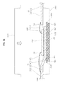
- FIG. 1 is a section view illustrating a mounting structure of a semiconductor device according to a first embodiment of the present disclosure.
- the mounting structure 801 of the semiconductor device shown in FIG. 1 includes a semiconductor device 101 , a substrate 807 and a heat radiation member 808 .
- a plurality of electronic parts is mounted on the substrate 807 .
- the substrate 807 is made of an insulating material.
- a wiring pattern not shown is formed in the substrate 807 .
- a plurality of holes 809 is formed in the substrate 807 .
- the heat radiation member 808 is made of a material having relatively high heat conductivity, e.g., a metal such as aluminum.
- the heat radiation member 808 is fixed with respect to the substrate 807 by a support member not shown.
- the semiconductor device 101 is mounted on the substrate 807 .
- the semiconductor device 101 is an article called an IPM (Intelligent Power Module).
- the semiconductor device 101 has applications in, e.g., an air conditioner or a motor control device.
- FIG. 2 is a (partially cut away) plan view of the semiconductor device according to the first embodiment of the present disclosure prior to bending the leads.
- FIG. 3 is a bottom view of the semiconductor device according to the first embodiment of the present disclosure prior to bending the leads.
- FIG. 4 is a section view taken along line IV-IV in FIG. 2 .
- FIG. 5 is a partially enlarged view of the region V in FIG. 4 .
- FIG. 1 corresponds to the cross section taken along line I-I in FIG. 2 .
- the respective components are schematically shown for the sake of understanding.
- the semiconductor device 101 shown in these figures includes a plurality of first electrode portions 1 , a plurality of second electrode portions 2 , a plurality of third electrode portions 3 , a plurality of semiconductor chips 41 and 42 , a plurality of passive chips 43 , a heat radiation layer 6 , a resin encapsulation portion 7 and wires 8 .
- the heat radiation layer 6 is indicated by a dotted line and the resin encapsulation portion 7 is indicated by an imaginary line.
- the resin encapsulation portion 7 covers the first electrode portions 1 , the second electrode portions 2 , the third electrode portions 3 , the semiconductor chips 41 and 42 and the passive chips 43 .
- the resin encapsulation portion 7 is made of, e.g., a black epoxy resin. As shown in FIGS. 3 and 4 , the resin encapsulation portion 7 has a resin major surface 71 , a resin bottom surface 72 and a resin side surface 73 .
- the resin major surface 71 is a smooth surface facing in the direction z 1 and extending along the x-y plane.
- the resin bottom surface 72 is a smooth surface facing in the direction 72 opposite to the direction z 1 and extending along the x-y plane.
- the resin side surface 73 is shaped to surround the semiconductor chips 41 and 42 and the passive chips 43 when seen in an x-y plane view. The resin side surface 73 is joined to the resin major surface 71 and the resin bottom surface 72 .
- a recess portion 75 is formed in the resin encapsulation portion 7 .
- the recess portion 75 is depressed from the resin bottom surface 72 .
- the recess portion 75 has a recess bottom surface 751 and a recess side surface 752 .
- the recess bottom surface 751 is shaped to extend along the x-y plane.
- the recess bottom surface 751 is an irregular surface having a fine concave-convex shape.
- the recess bottom surface 751 is converted to the irregular surface by subjecting the resin encapsulation portion 7 to a blasting process (to be described later).
- the height difference of the recess bottom surface 751 is in some embodiments, e.g., from 0.1 ⁇ m to 1 ⁇ m.
- the recess side surface 752 is joined to the recess bottom surface 751 and the resin bottom surface 72 .
- the recess side surface 752 is formed into a taper shape and is inclined with respect to the z direction.
- the recess side surface 752 is inclined with respect to the z direction such that, as the recess side surface 752 extends in the direction z 2 , the recess side surface 752 goes away from the recess bottom surface 751 when seen in an x-y plane view.
- the semiconductor chips 41 and 42 and the passive chips 43 have a rectangular shape when seen in a plan view.
- the semiconductor chips 41 are, e.g., power chips such as an IGBT, a MOS and a diode.
- the semiconductor chips 42 are, e.g., LSI chips such as a control IC.
- the passive chips 43 are, e.g., passives such as a resistor and a capacitor.
- the first electrode portions 1 , the second electrode portions 2 and the third electrode portions 3 shown in FIGS. 2 through 4 are all made of an electrically conductive material.
- the electrically conductive material may be, e.g., copper.
- the electrode portion shown in the right lower region in FIG. 2 is connected to the ground.
- Each of the first electrode portions 1 (four first electrode portions 1 in the present embodiment) includes a die pad section 11 (see FIGS. 1 , 2 and 4 ), a connecting section 12 (see FIGS. 1 and 2 ), a wire bonding section 13 (see FIGS. 1 and 2 ) and a lead 14 (see FIGS. 1 through 3 ).
- the first electrode portions 1 are spaced apart from one another in the x direction.
- Each of the die pad sections 11 is formed into a plate-like shape to extend along the x-y plane.
- Each of the semiconductor chips 41 is arranged in each of the die pad sections 11 .
- a joining layer 991 exists between each of the die pad sections 11 and each of the semiconductor chips 41 .
- the joining layer 991 is made of an electrically conductive material.
- the electrically conductive material is, e.g., a solder or a silver paste.
- the solder is relatively high in heat conductivity. If the solder is used as the joining layer 991 , it becomes possible to efficiently transfer heat from each of the semiconductor chips 41 to each of the die pad sections 11 .
- the die pad sections 11 are all exposed from the recess bottom surface 751 .
- Each of the die pad sections 11 has a die pad major surface 111 and a die pad rear surface 112 .
- the die pad major surface 111 faces in the direction z 1 .
- the die pad rear surface 112 faces in the direction z 2 . That is to say, the die pad major surface 111 and the die pad rear surface 112 face in opposite directions from each other.
- Each of the semiconductor chips 41 is arranged in the die pad major surface 111 .
- the joining layer 991 exists between the die pad major surface 111 and each of the semiconductor chips 41 .
- the die pad rear surface 112 is positioned in the same position as the recess bottom surface 751 in the thickness direction of the die pad sections 11 (in the z direction).
- the die pad rear surface 112 may be positioned at the open side of the recess portion 75 with respect to the recess bottom surface 751 .
- the die pad rear surface 112 is an irregular surface having a fine concave-convex shape.
- the die pad rear surface 112 is converted to the irregular surface by performing a blasting process to the die pad sections 11 (to be described later).
- the height difference of the die pad rear surface 112 is in some embodiments, e.g., from 0.01 ⁇ m to 1 ⁇ m.
- each of the connecting sections 12 is positioned between each of the die pad sections 11 and each of the wire bonding sections 13 and is joined to each of the die pad sections 11 and each of the wire bonding sections 13 .
- each of the connecting sections 12 is shaped to extend along a surface inclined with respect to the x-y plane.
- Each of the connecting sections 12 is inclined with respect to the x-y plane such that each of the connecting sections 12 extends in the direction z 1 as it goes away from each of the die pad sections 11 .
- Each of the wire bonding sections 13 shown in FIGS. 1 and 2 is shaped to extend along the x-y plane. Each of the wire bonding sections 13 is positioned in the z 1 direction with respect to each of the die pad sections 11 in the z direction.
- the wires 8 are bonded to each of the wire bonding sections 13 and each of the semiconductor chips 41 , whereby each of the wire bonding sections 13 and each of the semiconductor chips 41 are electrically connected to each other.
- Each of the leads 14 is joined to each of the wire bonding sections 13 .
- Each of the leads 14 extends along the y direction. Each of the leads 14 has a section protruding from the resin side surface 73 of the resin encapsulation portion 7 .
- the leads 14 are used for an insertion-mounting purpose. As shown in FIG. 1 , when the semiconductor device 101 is mounted on the substrate 807 , each of the leads 14 is bent and inserted into each of the holes 809 . A solder layer 810 fills each of the holes 809 in order to fix the leads 14 to the substrate 807 .
- each of the second electrode portions 2 (three second electrode portions 2 in the present embodiment) includes a wire bonding section 23 and a lead 24 .
- the second electrode portions 2 are spaced apart from one another in the x direction.
- Each of the wire bonding sections 23 is shaped to extend along the x-y plane. Each of the wire bonding sections 23 is positioned in the z 1 direction with respect to each of the die pad sections 11 in the z direction.
- the wires 8 are bonded to each of the wire bonding sections 23 and each of the semiconductor chips 41 , whereby each of the wire bonding sections 23 and each of the semiconductor chips 41 are electrically connected to each other.
- Each of the leads 24 is joined to each of the wire bonding sections 23 .
- Each of the leads 24 extends along the y direction.
- Each of the leads 24 has a section protruding from the resin side surface 73 of the resin, encapsulation portion 7 .
- the leads 24 are used for an insertion-mounting purpose. While not shown in the drawings, just like the leads 14 , each of the leads 24 is inserted into each of the holes 809 when the semiconductor device 101 is mounted on the substrate 807 .
- the third electrode portions 3 shown in FIGS. 1 and 2 include a plurality of control die pad sections 31 and a plurality of leads 32 .
- the control die pad sections 31 and the leads 32 are all arranged in the same position in the z direction.
- the semiconductor chips 42 or the passive chips 43 are arranged in the respective control die pad sections 31 .
- Joining layers exist between the control die pad sections 31 and the semiconductor chips 42 , and between the control die pad sections 31 and the passive chips 43 .
- the rear surfaces of the control die pad sections 31 may not face the heat radiation layer 6 and may not be exposed.
- Each of the leads 32 has a section protruding from the resin side surface 73 of the resin encapsulation portion 7 .
- the leads 32 are used for the insertion-mounting purpose. As shown in FIG. 1 , the leads 32 are inserted into the holes 809 when the semiconductor device 101 is mounted on the substrate 807 . As described above with respect to the leads 14 , a solder layer 810 fills the holes 809 in order to fix the leads 32 to the substrate 807 .
- the wires 8 are bonded to each of the leads 32 and each of the semiconductor chips 42 , whereby each of the leads 32 and each of the semiconductor chips 42 are electrically connected to each other.
- the wires 8 are also bonded to each of the semiconductor chips 42 and each of the passive chips 43 .
- the heat radiation layer 6 has an insulating property. As shown in FIG. 4 , the heat radiation layer 6 is arranged in the recess portion 75 of the resin encapsulation portion 7 . The heat radiation layer 6 is surrounded by the recess side surface 752 . In the present embodiment, the heat radiation layer 6 is formed into a plate-like shape to extend along the x-y plane. The heat radiation layer 6 makes direct contact with the die pad sections 11 on which the semiconductor chips 41 are mounted. More specifically, the heat radiation layer 6 makes direct, contact with the die pad rear surfaces 112 of the die pad sections 11 . The heat radiation layer 6 makes direct contact with the recess bottom surface 751 .
- the heat radiation layer 6 is spaced apart from the recess side surface 752 (at least a portion of the recess side surface 752 ).
- the heat radiation layer 6 has a section protruding from the resin bottom surface 72 .
- the heat radiation layer 6 is provided to rapidly dissipate the heat generated in the semiconductor chips 41 to the outside of the semiconductor device 101 .
- the heat radiation layer 6 may be made of a material higher in heat conductivity than the material of which the resin encapsulation portion 7 is made.
- the heat radiation layer 6 directly faces all the die pad sections 11 . As shown in FIG. 3 , the heat radiation layer 6 overlaps with all the respective die pad sections 11 when seen in an x-y plane view (when seen in the thickness direction of the heat radiation layer 6 ).
- the heat radiation layer 6 is called a heat radiation sheet (or a high-heat-conductivity sheet).
- the heat radiation layer 6 includes an elastic layer 69 .
- the elastic layer 69 is made of an insulating material. In the present embodiment, the heat radiation layer 6 is formed of only the elastic layer 69 .
- the elastic layer 69 is exposed in the direction, (the direction z 2 ) in which the recess portion 75 is opened. As shown in FIG. 3 , the elastic layer 69 overlaps with ail the die pad sections 11 when seen in the thickness direction z of the heat radiation layer 6 (when seen in an x-y plane view).
- the elastic layer 69 is a layer made of a material having a relatively small Young's modulus.
- the Young's modulus of the elastic layer 69 in some embodiments may be smaller than the Young's modulus of the resin encapsulation portion 7 .
- the heat radiation layer 6 is, e.g., a relatively soft sheet available before a thermosetting resin sheet is cured.
- the elastic layer 69 is made of, e.g., an epoxy-based resin.
- the elastic layer 69 may be made of a silicon rubber.
- the heat radiation layer 6 may be configured to include a base material and adhesive layers applied on the opposite surfaces of the base material. In that case, the adhesive layer makes up the elastic layer.
- the heat radiation layer 6 may be formed by applying an insulating paste on the recess portion 75 .
- the heat radiation layer 6 has a major surface 61 , a rear surface 62 and a side surface 63 .
- the major surface 61 faces in the direction z 1 .
- the major surface 61 overlaps with the die pad rear surface 112 of each of the die pad sections 11 and the recess bottom surface 751 .
- the major surface 61 of the heat radiation, layer 6 makes direct contact with the die pad rear surface 112 and the recess bottom surface 751 .
- the die pad rear surface 112 and the recess bottom surface 751 are irregular surfaces.
- the major surface 61 making direct contact with the die pad rear surface 112 and the recess bottom surface 751 is also formed of an irregular surface.
- the rear surface 62 faces in the direction z 2 opposite to the direction in which the major surface 61 faces.
- the rear surface 62 is not covered by the resin encapsulation portion 7 and is exposed.
- the side surface 63 feces in the direction perpendicular to the direction z, i.e., the thickness direction of the heat radiation layer 6 .
- the side surface 63 of the heat radiation layer 6 is spaced apart from the recess side surface 752 (at least a portion of the recess side surface 752 ).
- the heat radiation layer 6 is formed of only the elastic layer 69 . Therefore, the major surface 61 , the rear surface 62 and the side surface 63 of the heat radiation layer 6 are all made up of the elastic layer 69 .
- FIG. 10 is a section view illustrating the semiconductor device 101 mounted on the substrate 807 (see FIG. 1 ).
- the heat radiation layer 6 makes direct contact with the heat radiation member 808 in a state that the semiconductor device 101 is mounted on the substrate 807 .
- the rear surface 62 of the heat radiation layer 6 is pressed by the heat radiation member 808 toward the direction at which the recess bottom surface 751 is positioned.
- the heat radiation layer 6 is elastically deformed, thereby removing the gap between the heat radiation layer 6 and the recess side surface 752 . Consequently, the heat radiation layer 6 makes direct contact with the recess side surface 752 .
- the lead frame 300 including the die pad sections 11 , 31 , the semiconductor chips 41 and 42 and the passive chips 43 are prepared first. Then, as shown in FIG. 6 , each of the semiconductor chips 41 is arranged in one of the die pad sections 11 with the joining layer (not shown) interposed therebetween. Similarly, each of the semiconductor chips 42 and each of the passive chips 43 are arranged in one of the control die pad sections 31 with the joining layer (not shown) interposed therebetween. Subsequently, as shown in FIG. 6 , the wires 8 are bonded to the respective semiconductor chips 41 and 42 and so forth.
- the resin encapsulation portion 7 is formed.
- the resin encapsulation portion 7 is formed by a molding process using a mold 881 .
- the die pad sections 11 are pressed by the mold 881 .
- a resin material is injected into the mold 881 and is cured.
- the mold 881 is removed from the die pad sections 11 and so forth as shown in FIG. 8 .
- the resin encapsulation portion 7 can be formed.
- the recess portion 75 for exposing the die pad sections 11 is formed in the resin encapsulation portion 7 .
- the recess side surface 752 of the recess portion 75 is formed into a taper shape as set forth above.
- Thin resin burrs covering the die pad sections 11 are sometimes formed after formation of the resin encapsulation portion 7 .
- the die pad sections 11 are subjected to a blasting process (not shown).
- the blasting process refers to a method for roughening a surface by sputtering non-metallic particles, such as silica sands, or metallic particles at a high speed.
- non-metallic particles such as silica sands, or metallic particles at a high speed.
- the heat radiation layer 6 is formed in the recess portion 75 of the resin encapsulation portion 7 . More specifically, the heat radiation sheet as the heat radiation layer 6 is embedded into the recess portion 75 .
- the formation of the recess portion 75 in the resin encapsulation portion 7 allows the heat radiation sheet to be easily positioned with respect to each of the die pad sections 11 . Since the surface of the heat radiation sheet is relatively sticky, the heat radiation sheet itself is joined to the recess bottom surface 751 and the die pad rear surface 112 .
- the lead frame 300 shown in FIG. 6 is appropriately diced to thereby manufacture the semiconductor device 101 shown in FIG. 2 .
- the heat radiation layer 6 includes the elastic layer 69 .
- the elastic layer 69 is exposed in the direction (the direction z 2 ) in which the recess portion 75 is opened.
- the elastic layer 69 overlaps with each of the die pad sections 11 when seen in an x-y plane view.
- the elastic layer 69 is pressed by the heat radiation member 808 toward the recess bottom surface 751 when the semiconductor device 101 is mounted on the substrate 807 .
- the elastic layer 69 undergoes elastic deformation and makes close contact with the heat radiation member 808 .
- the elastic layer 69 and the heat radiation member 808 can be brought into close contact with each other, there is no need to interpose any heat radiating grease between the elastic layer 69 and the heat radiation member 808 . Therefore, it is not necessary that heat radiating grease be applied on the heat radiation member 808 each time the semiconductor device 101 is mounted on the substrate 807 . Accordingly, it is possible to efficiently mount the semiconductor device 101 to the substrate 807 .
- the semiconductor device 101 is not provided with the heat radiation plate mentioned in the section of background. It is therefore possible to reduce the cost involved in providing the heat radiation plate. Moreover, the thickness of the semiconductor device 101 can be reduced just as much as the thickness of the heat radiation plate.
- the resin encapsulation portion 7 has the resin bottom surface 72 .
- the recess portion 75 is depressed from the resin bottom surface 72 .
- the heat radiation layer 6 has a section protruding beyond the resin bottom surface 72 . With this configuration, even if the heat radiation layer 6 is elastically deformed, it is hard for the heat radiation member 808 to make contact with the resin bottom surface 72 . It is therefore possible to reliably bring the heat radiation layer 6 into close contact with, the heat radiation member 808 .
- the heat radiation layer 6 is elastically deformed.
- the gap between the heat radiation layer 6 and the recess side surface 752 is removed.
- the heat radiation layer 6 makes direct contact with recess side surface 752 .
- the heat radiation layer 6 and the recess side surface 752 can be spaced apart font each other through a gap in order to easily arrange the heat radiation sheet as the heat radiation layer 6 in the recess portion 75 .
- the heat radiation layer 6 can be brought into close contact with the recess side surface 752 in such a state that the semiconductor device 101 is mounted on the substrate 807 .
- the heat radiation layer 6 can be brought into close contact with the recess side surface 752 , the heat transferred from the die pad sections 11 to the resin encapsulation portion 7 can be transferred to the heat radiation member 808 by way of the recess bottom surface 751 and the heat radiation layer 6 . This assists in enhancing the heat dissipation of the semiconductor device 101 .
- each of the die pad sections 11 has the die pad rear surface 112 with which the heat radiation layer 6 makes direct contact.
- the die pad rear surface 112 is an irregular surface. With this configuration, it is possible to increase the joining area between the die pad rear surface 512 and the heat radiation layer 6 . If the joining area between the die pad rear surface 112 and the heat radiation layer 6 grows larger, the die pad rear surface 112 and the heat radiation layer 6 are strongly joined together. Therefore, the heat radiation layer 6 is hardly separated from the die pad rear surface 112 .
- the heat transferred from the semiconductor chips 41 to the die pad sections 11 can be readily transferred from the die pad sections 11 to the heat radiation layer 6 .
- the heat generated in the semiconductor chips 41 can be efficiently transferred outside of the semiconductor device 101 (to the heat radiation member 808 in the present embodiment) by way of the heat radiation layer 6 .
- the semiconductor device 101 is superior in heat dissipation. With the present embodiment, it is possible to provide the semiconductor device 101 capable of suppressing exfoliation of the heat, radiation layer 6 and performing superior heat dissipation.
- the recess bottom surface 751 is an irregular surface with which the heat radiation layer 6 makes direct contact. With this configuration, it is possible to increase the joining area between heat radiation layer 6 and the resin encapsulation portion 7 . If the joining area between heat radiation layer 6 and the resin encapsulation portion 7 grows larger, it is possible to restrain the heat radiation layer 6 from being separated from the resin encapsulation portion 7 .
- the resin encapsulation portion 7 is subjected to a blasting process, while a blasting process is performed on the die pad rear surface 112 .
- a blasting process is performed on the die pad rear surface 112 .
- FIGS. 11 through 22 A second embodiment of the present disclosure will now be described with reference to FIGS. 11 through 22 .
- FIG. 11 is a section view illustrating a mounting structure of a semiconductor device according to a second embodiment of the present disclosure.
- the mounting structure A 801 of the semiconductor device shown in FIG. 11 includes a semiconductor device A 100 , a substrate A 807 and a heat radiation member A 808 .
- a plurality of electronic parts is mounted on the substrate A 807 .
- the substrate A 807 is made of an insulating material.
- a wiring pattern not shown is formed in the substrate A 807 .
- a plurality of holes A 809 is formed in the substrate A 807 .
- the heat radiation member A 808 is made of a material having relatively high heat conductivity, e.g., a metal such as aluminum.
- the heat radiation member A 808 is fixed with respect to the substrate A 807 by a support member not shown.
- the semiconductor device A 100 is mounted on the substrate A 807 .
- the semiconductor device A 100 is an article called an IPM (Intelligent Power Module).
- the semiconductor device A 100 can find its application in, e.g., an air conditioner or a motor control device.
- FIG. 12 is a (partially cut away) plan view of the semiconductor device according to the second embodiment of the present disclosure prior to bending the leads.
- FIG. 13 is a bottom view of the semiconductor device according to the second, embodiment of the present disclosure prior to bending the leads.
- FIG. 14 is a section view taken along line XIV-XIV in FIG. 12 .
- FIG. 15 is a section view taken along line XV-XV in FIG. 12 .
- the semiconductor device A 100 shown in these figures includes first electrode portions A 1 , second electrode portions A 2 , third electrode portions A 3 , semiconductor chips A 41 and A 42 , passive chips A 43 , a heat radiation plate A 6 , a resin encapsulation portion A 7 , wires A 8 and a joining layer A 991 .
- the resin encapsulation portion A 7 is not shown and is indicated by a double-dot chain line.
- the resin encapsulation portion A 7 shown in FIGS. 13 through 15 covers the first electrode portions A 1 , the second electrode portions A 2 , the third electrode portions A 3 , the semiconductor chips A 41 and A 42 , the passive chips A 43 , the heat radiation plate A 6 , the wires A 8 and the joining layer A 991 .
- the resin encapsulation portion A 7 is made of an insulating resin.
- the insulating resin may be, e.g., a black epoxy resin.
- the resin encapsulation portion A 7 has a resin major surface A 71 , a resin bottom surface A 72 and a resin side surface A 73 .
- the resin major surface A 71 is a smooth surface facing in the direction z 1 and extends along the x-y plane.
- the resin bottom, surface A 72 is a smooth surface facing in the direction z 2 opposite to the direction z 1 and extends along the x-y plane.
- the resin side surface A 73 is shaped to surround die semiconductor chips A 41 and A 42 and the passive chips A 43 when seen in an x-y plane view.
- the resin side surface A 73 is joined to the resin major surface A 71 and the resin bottom surface A 72 .
- the resin encapsulation portion A 7 includes a plurality of intermediate sections A 75 .
- the intermediate sections A 75 will be described later.
- the semiconductor chips A 41 and A 42 and the passive chips A 43 have a rectangular shape when seen in a plan view.
- the semiconductor chips A 41 are, e.g., power chips such as an IGBT, a MOS and a diode.
- the semiconductor chips A 42 are, e.g., LSI chips such as a control IC.
- the passive chips A 43 are, e.g., passives such as a resistor and a capacitor.
- the first electrode portions A 1 , the second electrode portions A 2 and the third electrode portions A 3 shown in FIGS. 12 through 15 have electric conductivity.
- the first electrode portions A 1 , the second electrode portions A 2 and the third electrode portions A 3 are all made of an electrically conductive material.
- the electrically conductive material may be, e.g., copper.
- the electrode portion shown in the right lower region in FIG. 12 is connected to the ground.
- Each of the first electrode portions A 1 (four first electrode portions A 1 in the present embodiment) includes a die pad section A 11 (see FIGS. 11 through 14 ), a connecting section A 12 (see FIGS. 11 and 12 ), a wire bonding section A 13 (see FIGS. 11 and 12 ) and a lead A 14 (see FIGS. 11 and 12 ).
- the first electrode portions A 1 are spaced apart from one another in the x direction.
- Each of the die pad sections A 11 is formed into a plate-like shape to extend along the x-y plane.
- the semiconductor chips A 41 are arranged in the die pad sections A 11 . More specifically, the semiconductor chips A 41 which generate heat easily are joined to the die pad sections A 11 .
- Each of the die pad sections A 11 has a die pad major surface A 111 and a die pad rear surface A 112 .
- the die pad major surface A 111 faces in the direction z 1 .
- the die pad rear surface A 112 feces in the direction z 2 . That is to say, the die pad major surface A 111 and the die pad rear surface A 112 face toward the opposite directions from each other.
- Each of the semiconductor chips A 41 is arranged in the die pad major surface A 111 . More specifically, each of the semiconductor chips A 41 is joined to the die pad major surface A 111 .
- the joining layer A 991 exists between the die pad major surface A 111 and each of the semiconductor chips A 41 .
- each of the connecting sections A 12 is positioned between each of the die pad sections A 11 and each of the wire bonding sections A 13 and is joined to each of the die pad sections A 11 and each of the wire bonding sections A 13 .
- Each of the connecting sections A 12 is shaped to extend along a surface inclined with respect to the x-y plane.
- Each of the connecting sections A 12 is inclined with respect to the x-y plane such that each of the connecting sections A 12 extends in the direction z 1 as it goes away from each of the die pad sections A 11 .
- Each of the wire bonding sections A 13 shown in FIGS. 11 , 12 and 15 is shaped to extend along the x-y plane. Each of the wire bonding sections A 13 is positioned in the z 1 direction with respect to each of the die pad sections A 11 in the direction z.
- the wires A 8 are bonded to each of the wire bonding sections A 13 and each of the semi conductor chips A 41 , whereby each of the wire bonding sections A 13 and each of the semiconductor chips A 41 are electrically connected to each other.
- Each of the leads A 14 is joined to each of the wire bonding sections A 13 . Each of the leads A 14 extends along the direction y.
- Each of the leads A 14 has a section protruding from the resin side surface A 73 of the resin encapsulation portion A 7 .
- each of the leads A 14 is used for an insertion-mounting purpose. As shown in FIG. 11 , when the semiconductor device A 100 is mounted on the substrate A 807 , each of the leads A 14 is bent and inserted into each of the holes A 809 . A solder layer A 810 fills each of the holes A 809 in order to fix the leads A 14 to the substrate A 807 .
- each of the second electrode portions A 2 (three second electrode portions A 2 in the present embodiment) includes a wire bonding section A 23 and a lead A 24 .
- the second electrode portions A 2 are spaced apart from one another in the x direction.
- Each of the wire bonding sections A 23 is shaped to extend along the x-y plane. Each of the wire bonding sections A 23 is positioned in the z 1 direction with respect to each of the die pad sections A 11 in the direction z.
- the wires 8 are bonded to each of the wire bonding sections A 23 and each of the semiconductor chips A 41 , whereby each of the wire bonding sections A 23 and each of the semiconductor chips A 41 are electrically connected to each other.
- Each of the leads A 24 is joined to each of the wire bonding sections A 23 .
- Each of the leads A 24 extends along the direction y.
- Each of the leads A 24 has a section protruding from the resin side surface A 73 of the resin encapsulation portion A 7 .
- the leads A 24 are used for an insertion-mounting purpose. While not shown in the drawings, just like the leads 14 , the leads A 24 are inserted into the holes A 809 when, the semiconductor device A 100 is mounted on the substrate A 807 .
- the third electrode portions A 3 shown in FIGS. 11 and 12 include a plurality of control die pad sections A 31 and a plurality of leads A 32 .
- the control die pad sections A 31 and the leads A 32 are ail arranged in the same position in the z direction.
- the semiconductor chips A 42 or the passive chips A 43 are arranged in the respective control die pad sections A 31 .
- a joining layer (not shown) exists between the control die pad sections A 31 and the semiconductor chips A 42 , and between the control die pad sections A 31 and the passive chips A 43 .
- the rear surfaces of the control die pad sections A 31 may not face the heat radiation plate A 6 and may not be exposed.
- Each of the leads A 32 has a section protruding from the resin side surface A 73 of the resin encapsulation portion A 7 .
- the leads A 32 are used for an insertion-mounting purpose. As shown in FIG. 11 , the leads A 32 are inserted into the holes A 809 when the semiconductor device A 100 is mounted on the substrate A 807 . As described above with respect to the leads 14 , a solder layer A 810 fills the holes A 809 in order to fix the leads A 32 to the substrate A 807 .
- the wires A 8 are bonded to each of the leads A 32 and each of the semiconductor chips A 42 , whereby each of the leads A 32 and each of the semiconductor chips A 42 are electrically connected to each other.
- the wires A 8 are also bonded to each of the semiconductor chips A 42 and each of the passive chips A 43 .
- the joining layer A 991 exists between each of the die pad sections A 11 and each of the semiconductor chips A 41 .
- the joking layer A 991 joins each of the semiconductor chips A 41 to each of the die pad sections A 11 .
- the joining layer A 991 is made of, e.g., an electrically conductive material.
- the electrically conductive material may be, e.g., a silver paste or a solder.
- the solder is relatively high in heat conductivity. If the solder is used as the joining layer A 991 , it becomes possible to efficiently transfer heat from each of the semiconductor chips A 41 to each of the die pad sections A 11 .
- the joining layer A 991 may be made of an insulating material instead of the electrically conductive material.
- the heat radiation plate A 6 directly faces the die pad sections A 11 .
- the heat radiation plate A 6 is formed into a plate-like shape to extend along the x-y plane.
- the heat radiation plate A 6 is spaced apart from the die pad sections A 11 .
- the intermediate sections A 75 mentioned above exist, between the heat radiation plate A 6 and the die pad sections A 11 .
- the intermediate sections A 75 make direct contact with the heat radiation plate A 6 and the die pad sections A 11 . Therefore, the heat radiation plate A 6 and the die pad sections A 11 are joined by the resin encapsulation portion A 7 .
- the material making up the intermediate sections A 75 is the same as the material making up the section of the resin encapsulation portion A 7 that covers the semiconductor chips A 41 and A 42 .
- the heat radiation plate A 6 is exposed from the resin bottom surface A 72 of the resin encapsulation portion A 7 .
- the heat radiation plate A 6 is provided to rapidly dissipate the heat generated in the semiconductor chips A 41 outside of the semiconductor device A 100 .
- the heat conductivity of the material making up the heat radiation plate A 6 becomes larger.
- the heat radiation plate A 6 may be made of a material higher in heat conductivity than the material of which the resin encapsulation portion A 7 is made. More specifically, the heat radiation plate A 6 is made of a material higher in heat conductivity than the material of which the die pad sections A 11 are made.
- the heat radiation plate A 6 is made of, e.g., an electrically conductive material.
- the electrically conductive material may be, e.g., aluminum, copper, copper alloy or iron.
- the heat radiation plate A 6 may be silver-plated aluminum.
- the heat radiation plate A 6 may be made of an insulating material.
- the insulating material may be, e.g., ceramic. Examples of the ceramic include alumina, aluminum nitride and silicon nitride.
- the heat radiation plate A 6 is made of an electrically conductive material.
- the clearance between the heat radiation plate A 46 and die pad sections A 11 may be in some embodiments, e.g., from 20 ⁇ m to 200 ⁇ m. If the clearance between the heat radiation plate A 6 and die pad sections A 11 is too small, there is an increasing possibility that the die pad sections A 11 are electrically connected to one another via the heat radiation plate A 6 . On the other hand, if the clearance between the heat radiation plate A 6 and die pad sections A 11 becomes too large, the transfer of the heat generated in the semiconductor chips A 41 to the heat radiation plate A 6 is cut off by the intermediate sections A 75 . Thus it is hard to transfer the heat generated in the semiconductor chips A 41 to fee heat radiation plate A 6 .
- the heat radiation plate A 6 overlaps with all the die pad sections A 11 when seen in an x-y plane view. While the semiconductor device A 100 is provided with only one heat radiation plate A 6 the semiconductor device A 100 may be provided with a plurality of heat radiation plates, if the semiconductor device A 100 is provided with a plurality of heat radiation plates, each of the heat radiation plates overlaps with one of the die pad sections A 11 when seen in an x-y plane view.
- the heat radiation plate A 6 has a major surface A 61 , a rear surface A 62 and a side surface A 63 .
- the major surface A 61 of the heat radiation plate A 6 directly feces the die pad rear surface A 112 of each of the die pad sections A 11 .
- the major surface A 61 is spaced apart from the die pad sections A 11 .
- the aforementioned intermediate sections A 75 exist between the major surface A 61 of the heat radiation plate and the die pad sections A 11 .
- the major surface A 61 and the die pad sections A 11 make direct contact with the intermediate sections A 75 .
- the major surface A 61 is smooth.
- the major surface A 61 in other embodiments may not be smooth but may have a concave-convex section.
- the concave-convex section may be arranged near the intermediate sections A 75 .
- the rear surface A 62 faces an opposite direction to which the major surface A 61 faces.
- the resin bottom surface A 72 faces the same direction as the rear surface A 62 of the heat radiation plate A 6 faces.
- the rear surface A 62 is exposed from fee resin bottom surface A 72 of the resin encapsulation portion A 7 .
- the rear surface A 62 is flush with the resin bottom surface A 72 .
- the side surface A 63 is smooth and is perpendicular to the rear surface A 62 .
- the side surface A 63 of the heat radiation plate A 6 as a whole is covered by the resin encapsulation portion A 7 .
- the heat radiation plate A 6 includes dropout prevention units A 691 .
- the dropout prevention units A 691 are provided to prevent the heat radiation plate A 6 from being dropped out (detached) from the resin encapsulation portion A 7 .
- the dropout prevention units A 691 protrude from the rear surface A 62 of the heat radiation plate when seen in the thickness direction z of the die pad sections A 11 (when seen in an x-y plane view).
- the dropout prevention units A 691 are positioned, to face the major surface A 61 with respect to the resin encapsulation portion A 7 . That is to say, a portion, of the resin encapsulation portion A 7 is positioned in the z 2 direction of the dropout prevention units A 691 .
- the dropout prevention units A 691 are shaped to protrude from the side surface A 63 of the heat radiation plate in the direction orthogonal to the direction z.
- the lead frame A 300 including the die pad sections A 11 and A 31 , the semiconductor chips A 41 and A 42 and the passive chips A 43 are prepared first. Then, as shown in FIG. 16 , each of the semiconductor chips A 41 is arranged in one of the die pad sections A 11 with the joining layer (not shown) interposed therebetween. Similarly, each of the semiconductor chips A 42 and each of the passive chips A 43 are arranged in one of the control die pad sections A 31 with the joining layer (not shown) interposed therebetween. Subsequently, as shown in FIG. 16 , the wires A 8 are bonded to the respective semiconductor chips A 41 and A 42 and so forth.
- a first mold A 881 and a second mold A 882 shown in FIGS. 17 and 18 are prepared.
- the resin encapsulation portion A 7 is formed using the first mold A 881 and the second mold A 882 .
- the heat radiation plate A 6 is arranged in the first mold A 881 .
- the lead frame A 300 is placed on the edge of the first mold A 881 (see FIG. 18 ).
- a gap is formed between the heat radiation plate A 6 and the die pad sections A 11 .
- the heat radiation plate A 6 , the die pad sections A 11 , the semiconductor chips A 41 and A 42 , the passive chips A 43 and the wires A 8 are enclosed by the first mold A 881 and the second mold A 882 .
- a resin material is injected into the space surrounded by the first mold A 881 and the second mold A 882 .
- the heat radiation plate A 6 and the die pad sections A 11 are not bonded to each other.
- the resin material is cured after it is injected into the space surrounded by the first mold A 881 and the second mold A 882 .
- the resin encapsulation portion A 7 shown in FIGS. 21 and 22 is formed by curing the resin material. As the resin material is cured, the heat radiation plate A 6 and the die pad sections A 11 are joined together. Then, as shown in FIGS. 21 and 22 , the first mold A 881 and the second mold A 882 are removed from the resin encapsulation portion A 7 .
- the lead frame A 300 shown in FIG. 16 is appropriately diced to thereby manufacture the semiconductor device A 100 shown in FIG. 12 .
- the heat radiation plate A 6 and the die pad sections A 11 are joined together by the resin encapsulation portion A 7 when forming the resin encapsulation portion A 7 .
- this configuration it is not necessary to join the heat radiation plate A 6 and the die pad sections A 11 through a joining layer other than the resin encapsulation portion A 7 . For that reason, it is possible to reduce the cost involved in providing a joining layer for joining the heat radiation plate A 6 and the die pad sections A 11 .
- the heat radiation plate A 6 and the die pad sections A 11 can be joined together simultaneously while forming the resin encapsulation portion A 7 .
- FIGS. 23 through 26 A first modified example of the second embodiment of the present disclosure will be described with reference to FIGS. 23 through 26 .
- FIG. 23 is a section view illustrating a semiconductor device according to a first modified example of the second embodiment of the present disclosure.
- FIG. 24 is a section view illustrating the semiconductor device according to the first modified example of the second embodiment of the present disclosure.
- the semiconductor device A 101 shown in these figures includes first electrode portions A 1 , second electrode portions A 2 , third electrode portions A 3 , semiconductor chips A 41 and A 42 , passive chips A 43 , a heat radiation plate A 6 , an resin encapsulation portion A 7 , wires A 8 and a joining layer A 991 . Except for the heat radiation plate A 6 , the respective components of the semiconductor device A 101 including the first electrode portions A 1 , the second electrode portions A 2 , the third electrode portions A 3 , the semiconductor chips A 41 and A 42 , the passive chips A 43 , the resin encapsulation portion A 7 , the wires A 8 and the joining layer A 991 are the same as the respective components of the semiconductor device A 100 and, therefore, will not be described.
- the heat radiation plate A 6 has a major surface A 61 , a rear surface A 62 and a side surface A 63 .
- the major surface A 61 is the same as that of the semiconductor device A 100 and, therefore, will not be described.
- the rear surface A 62 faces an opposite direction from which the major surface A 61 faces.
- the rear surface A 62 is exposed from the resin bottom surface A 72 of the resin encapsulation portion A 7 .
- the heat radiation plate A 6 has a section protruding toward the facing direction of the rear surface A 62 (the direction z 2 ) beyond the resin bottom surface A 72 . For that reason, the rear surface A 62 is positioned at the direction z 2 with respect to the resin bottom surface A 72 .
- the rear surface A 62 makes contact with the heat radiation member A 808 .
- the side surface A 63 is smooth and is perpendicular to the rear surface A 62 .
- a portion of the side surface A 63 is covered by the resin encapsulation portion A 7 and a portion of the side surface A 63 is exposed from the resin encapsulation portion A 7 .
- the side surface A 63 as a whole may be covered by the resin encapsulation portion A 7 .
- the article shown in FIG. 16 is manufactured through the same processes as described with respect to the semiconductor device A 100 .
- a first mold A 881 and a second mold A 882 shown in FIGS. 25 and 26 are prepared.
- the resin encapsulation portion A 7 is formed using the first mold A 881 and the second mold A 882 .
- a recess portion A 885 is formed in the first mold A 881 .
- the plan-view size of the recess portion A 885 is a little larger than the plan-view size of the heat radiation plate A 6 .
- the heat radiation plate A 6 is arranged in the first mold A 881 .
- the heat radiation plate A 6 is arranged in the recess portion A 885 of the first mold A 881 (see FIG. 26 ).
- the lead frame A 300 is placed on the edge of the first mold A 881 .
- a gap is formed between the heat radiation plate A 6 and the die pad sections A 11 .
- the heat radiation plate A 6 , the die pad sections A 11 , the semiconductor chips A 41 and A 42 , the passive chips A 43 and the wires A 8 are enclosed by the first mold A 881 and the second mold A 882 .
- a resin material is injected into the space surrounded by the first mold A 881 and the second mold A 882 .
- the heat radiation, plate 46 and the die pad sections A 11 are not bonded to each other.
- the resin material is cured after it is injected into the space surrounded by the first mold A 883 and the second mold A 882 .
- the resin encapsulation portion A 7 is formed by curing the resin material. As the resin material is cured, the heat radiation plate A 6 and the die pad sections A 11 are joined together. Then, the first mold A 881 and the second mold A 882 are removed from the resin encapsulation portion A 7 .
- the lead frame A 300 is appropriately diced to thereby manufacture fee semiconductor device A 101 .
- the heat radiation plate A 6 has a section protruding toward the facing direction of the rear surface A 62 (the z 2 direction) beyond the resin bottom surface A 72 . For that reason, the rear surface A 62 is positioned in the z 2 direction with respect to the resin bottom surface A 72 . With this configuration, it is hard to for the heat radiation member A 808 to be contact with the resin bottom surface A 72 . This makes it easy to bring the rear surface A 62 of the heat radiation plate A 6 into contact with the heat radiation member A 808 . Accordingly, the heat transferred from the semiconductor chips A 41 to the heat radiation plate A 6 can be efficiently transferred to the heat radiation member A 808 .
- the first mold A 881 having the recess portion A 885 is used in manufacturing the semiconductor device A 101 . Since the heat radiation plate A 6 is arranged in the recess portion A 885 , it is possible to prevent the heat radiation plate A 6 from moving within the space by the flow of the resin material when the resin material is injected into the space surrounded by the first mold A 881 and the second mold A 882 . With the present modified example, it is therefore possible to precisely arrange the heat radiation plate A 6 in a desired position.
- FIGS. 27 through 28 A second modified example of the second embodiment of the present disclosure will be described with reference to FIGS. 27 through 28 .
- FIGS. 27 and 28 are section views illustrating a semiconductor device according to a second modified example of the second embodiment of the present disclosing.
- the semiconductor device A 102 shown in these figures includes first electrode portions A 1 , second electrode portions A 2 , third electrode portions A 3 , semiconductor chips A 41 and A 42 , passive chips A 43 , a heat radiation plate A 6 , a resin encapsulation portion A 7 , wires A 8 and a joining layer A 991 . Except for the heat radiation plate A 6 , the respective components of the semiconductor device A 102 including the first electrode portions A 1 , the second electrode portions A 2 , the third electrode portions A 3 , the semiconductor chips A 41 and A 42 , the passive chips A 43 , the resin encapsulation portion A 7 , the wires A 8 and the joining layer A 991 are the same as the respective components of the semiconductor device A 100 and, therefore, will not be described.
- the heat radiation plate A 6 of the present modified example differs from the heat radiation plate A 6 of the semiconductor device A 100 in terms of the cross-sectional shape.
- the heat radiation plate A 6 has a major surface A 61 , a rear surface A 62 and a side surface A 63 .
- the major surface A 61 and the rear surface A 62 are the same as those of the semiconductor device A 100 and, therefore, will not be described.
- the side surface A 63 has a curved surface shape.
- the side surface A 63 as a whole is covered by the resin encapsulation portion A 7 .
- the manufacturing method of the semiconductor device A 102 for the same reason as described above with respect to the semiconductor device A 100 , it is possible to reduce the manufacturing cost and to enhance the manufacturing efficiency. Further, according to the present modified example, the curved shape of the side surface A 63 can improve its manufacturability. Also, the resin encapsulation portion A 7 covered on the side surface A 63 can prevent foam (or bubbles) from forming on the side surface A 63 .
- FIGS. 29 through 30 A third modified example of the second embodiment of the present disclosure will be described with reference to FIGS. 29 through 30 .
- FIGS. 29 and 30 are section views illustrating a semiconductor device according to a third modified example of the second embodiment of the present, disclosure.
- the semiconductor device A 103 shown in these figures includes first electrode portions A 1 , second electrode portions A 2 , third electrode portions A 3 , semiconductor chips A 41 and A 42 , passive chips A 43 , a heat radiation plate A 6 , an resin encapsulation portion A 7 , wires A 8 and a joining layer A 991 . Except the heat radiation plate A 6 , the respective components of the semiconductor device A 103 including the first electrode portions A 1 , the second electrode portions A 2 , the third electrode portions A 3 , the semiconductor chips A 41 and A 42 , the passive chips A 43 , the resin encapsulation portion A 7 , the wires A 8 and the joining layer A 991 are the same as the respective components of the semiconductor device A 102 and, therefore, will not be described.
- the heat radiation plate A 6 has a major surface A 61 , a rear surface A 62 and a side surface A 63 .
- the major surface A 61 is the same as that of the semiconductor device A 102 and, therefore, will not be described.
- the rear surface A 62 faces in an opposite direction from which the major surface A 61 faces.
- the rear surface A 62 is exposed from the resin bottom surface A 72 of the resin encapsulation portion A 7 .
- the heat radiation plate A 6 has a section protruding toward the facing direction of the rear surface A 62 (the z 2 direction) beyond the resin bottom surface A 72 . For that reason, the rear surface A 62 is positioned in the z 2 direction with respect to the resin bottom surface A 72 .
- the side surface A 63 has a curved surface shape. A portion of the side surface A 63 is covered by the resin encapsulation portion A 7 and a portion of the side surface A 63 is exposed from the resin encapsulation portion A 7 . Unlike the present modified example, the side surface A 63 as a whole may be covered by the resin encapsulation portion A 7 .
- the semiconductor device A 103 When manufacturing the semiconductor device A 103 , it may be possible to use the first mold A 881 having a recess portion A 885 , which is the same as used in manufacturing the semiconductor device A 101 .
- the heat transferred from the semiconductor chips A 41 to the heat radiation plate A 6 can be efficiently transferred to the heat radiation member A 808 .
- FIGS. 31 and 32 are section views illustrating a semiconductor device according to a fourth modified example of the second embodiment of the present disclosure.
- the semiconductor device A 104 shown in these figures differs from the semiconductor device A 100 in that the semiconductor device A 104 further includes a plurality of spacers A 799 .
- the respective spacers A 799 exist between the die pad sections A 11 and the heat radiation plate A 6 .
- the respective spacers A 799 make direct contact with the die pad sections A 11 and the heat radiation plate A 6 .
- the respective spacers A 799 are made of an insulating material.
- each of the spacers A 799 has a cubical shape.
- each of the spacers A 799 may have a spherical shape, a rod-like shape or other shapes.
- the spacers A 799 are covered by the intermediate sections A 75 of the resin encapsulation portion A 7 .
- the spacers A 799 define the clearance between the die pad sections A 11 and the heat radiation plate A 6 . Accordingly, it is possible to accurately position the die pad sections A 11 with respect to the heat radiation plate A 6 .
- the configuration provided with the spacers A 799 may be applied to one of the semiconductor devices A 101 , A 102 and A 103 .
- FIGS. 33 through 36 A third embodiment of the present disclosure will be described with reference to FIGS. 33 through 36 .
- FIGS. 33 and 34 are section views illustrating a semiconductor device according to a third embodiment of the present disclosure.
- the semiconductor device A 200 shown in these figures includes first electrode portions A 1 , second electrode portions A 2 , third electrode portions A 3 , semiconductor chips A 41 and A 42 , passive chips A 43 , a heat radiation plate A 6 , an resin encapsulation portion A 7 , wires A 8 and a joining layer A 991 . Except for the heat radiation plate A 6 and the resin encapsulation portion A 7 , the respective components of the semiconductor device A 200 including the first electrode portions A 1 , the second electrode portions A 2 , the third electrode portions A 3 , the semiconductor chips A 41 and A 42 , the passive chips A 43 , the wires 8 and the joining layer A 991 are the same as the respective components of the semiconductor device A 100 and, therefore, will not be described.
- the resin encapsulation portion A 7 of the present embodiment remains the same as the configuration of the semiconductor device A 100 except that the resin encapsulation portion A 7 does not include the intermediate sections A 75 stated above.
- the heat radiation plate A 6 directly faces the die pad sections A 11 .
- the heat radiation plate A 6 of the present embodiment is formed into a plate-like shape to extend along the x-y plane.
- the heat radiation plate A 6 makes direct contact with the die pad sections A 11 .
- the heat radiation plate A 6 is exposed from the resin bottom surface A 72 of the resin encapsulation portion A 7 .
- the heat radiation plate A 6 is provided to rapidly dissipate the heat generated in the semiconductor chips A 41 to the outside of the semiconductor device A 200 .
- the heat conductivity of the material making up the heat radiation plate A 6 becomes larger.
- the heat radiation plate A 6 may be made of a material higher in heat conductivity than the material of which the resin encapsulation portion A 7 is made. More specifically, the heat radiation plate A 6 is made of a material higher in heat conductivity than the material of which the die pad sections A 11 are made.
- the heat radiation plate A 6 may be made of an insulating material.
- the insulating material may be, e.g., ceramic. Examples of the ceramic include alumina, aluminum nitride and silicon nitride.
- the heat radiation plate A 6 overlaps with all the die pad sections A 11 when seen in an x-y plane view (see FIG. 13 ). While the semiconductor device A 200 is provided with only one heat radiation plate A 6 , the semiconductor device A 200 may be provided with a plurality of heat radiation plates. When the semiconductor device A 200 is provided with a plurality of heat radiation plates, each of the heat radiation plates overlaps with one of the die pad sections A 11 when seen in an x-y plane view.
- the heat radiation plate A 6 has a major surface A 61 , a rear surface A 62 and a side surface A 63 .
- the major surface A 61 directly faces the die pad rear surface A 112 of each of the die pad sections A 11 .
- the major surface A 61 makes direct contact with the die pad rear surface A 112 of each of the die pad sections A 11 .
- the major surface A 61 is smooth.
- the rear surface A 62 and the side surface A 63 are the same as those of the semiconductor device A 100 and, therefore, will not be described.
- the heat radiation plate A 6 includes dropout prevention units A 691 .
- the dropout prevention units A 691 are the same as those of the semiconductor device A 100 and, therefore, will not be described.
- the article shown in FIG. 16 is manufactured through the same process as described with respect to the semiconductor device A 100 .
- a first mold A 881 and a second mold A 882 shown in FIGS. 35 and 36 are prepared.
- the resin encapsulation portion A 7 is formed using the first mold A 881 and the second mold A 882 .
- the heat radiation plate A 6 is arranged in the first mold A 881 .
- the lead frame A 300 is placed on the edge of the first mold A 881 .
- the heat radiation plate A 6 and the die pad sections A 11 make direct contact with each other.
- the heat radiation plate A 6 , the die pad sections A 11 , the semiconductor chips A 41 and A 42 , the passive chips A 43 and the wires A 8 are enclosed by the first mold A 881 and the second mold A 882 (not shown).
- a resin material is injected into the space surrounded by the first mold A 881 and the second mold A 882 .
- the resin material is injected into the space surrounded, by the first mold A 881 and the second mold A 882 , the heat radiation plate A 6 and the die pad sections A 11 are not bonded to each other.
- the resin material is cured after it is injected into the space surrounded by the first mold A 881 and the second mold A 882 .
- the resin encapsulation portion A 7 is formed by curing the resin material. As die resin material is cured, the heat radiation plate A 6 and the die pad sections A 11 are joined together. Then, the first mold A 881 and the second mold A 882 are removed from the resin encapsulation portion A 7 .
- the lead frame A 300 is appropriately diced to thereby manufacture the semiconductor device A 200 .
- a first modified example of the third embodiment of the present disclosure wilt be described with reference to FIGS. 37 and 38 .
- FIGS. 37 and 38 are section views illustrating a semiconductor device according to a first modified example of the third embodiment of the present disclosure.
- the semiconductor device A 201 corresponds to the combination of the configuration of the semiconductor device A 200 and the configuration of the semiconductor device A 101 . More specifically, the semiconductor device A 201 is configured as follows.
- the semiconductor device A 201 includes first electrode portions A 1 , second electrode portions A 2 , third electrode portions A 3 , semiconductor chips A 41 and A 42 , passive chips A 43 , a heat radiation plate A 6 , a resin encapsulation portion A 7 , wires A 8 and a joining layer A 991 . Except for the heat radiation plate A 6 , the respective components of the semiconductor device A 201 including the first, electrode portions A 1 , the second electrode portions A 2 , the third electrode portions A 3 , the semiconductor chips A 41 and A 42 , the passive chips A 43 , the resin encapsulation portion A 7 , the wires A 8 and the joining layer A 991 are the same as the respective components of the semiconductor device A 200 and, therefore, will not be described.
- the heat radiation plate A 6 has a major surface A 61 , a rear surface A 62 and a side surface A 63 .
- the major surface A 61 is the same as that of the semiconductor device A 200 and, therefore, will not be described.
- the rear surface A 62 faces a direction opposite from which the heat radiation plate major surface A 61 faces.
- the rear surface A 62 is exposed from the resin bottom surface A 72 of the resin encapsulation portion A 7 .
- the heat radiation plate A 6 has a section protruding toward the lacing direction of the rear surface A 62 (the direction z 2 ) beyond the resin bottom surface A 72 . For that reason, the rear surface A 62 is positioned in the direction z 2 with respect to the resin bottom surface A 72 .
- the rear surface A 62 makes contact with the heat radiation member A 808 .
- the side surface A 63 is smooth and is perpendicular to the rear surface A 62 .
- a portion of the side surface A 63 is covered by the resin encapsulation portion A 7 and a portion of the side surface A 63 is exposed from the resin encapsulation portion A 7 .
- the side surface A 63 as a whole may be covered by the resin encapsulation portion A 7 .
- the semiconductor device A 201 can be manufactured in the same method as the manufacturing method of the semiconductor device A 101 .
- the heat transferred from the semiconductor chips A 41 to the heat radiation plate A 6 can be efficiently transferred to the heat radiation member A 808 .
- FIGS. 39 and 40 are section views illustrating a semiconductor device according to a second modified example of the third embodiment of the present disclosure.
- the semiconductor device A 202 corresponds to the combination of the configuration of the semiconductor device A 200 and the configuration of the semiconductor device A 102 . More specifically, the semiconductor device A 202 is configured as follows.
- the semiconductor device A 202 includes first electrode portions A 1 , second electrode portions A 2 , third electrode portions A 3 , semiconductor chips A 41 and A 42 , passive chips A 43 , a heat radiation plate A 6 , an resin encapsulation portion A 7 , wires A 8 and a joining layer A 991 . Except for the heat radiation plate A 6 , the respective components of the semiconductor device A 202 including me first electrode portions A 1 , the second electrode portions A 2 , the third electrode portions A 3 , the semiconductor chips A 41 and A 42 , the passive chips A 43 , the resin encapsulation portion A 7 , the wires A 8 and the joining layer A 991 are the same as the respective components of the semiconductor device A 200 and, therefore, will not be described.
- the heat radiation plate A 6 of the present modified example differs from the heat radiation plate A 6 of the semiconductor device A 200 in terms of the cross-sectional shape.
- the heat radiation plate A 6 has a major surface A 61 , a rear surface A 62 and a side surface A 63 .
- the major surface A 61 and the rear surface A 62 are the same as those of the semiconductor device A 200 and, therefore, will not be described.
- the side surface A 63 has a curved surface shape.
- the side surface A 63 as a, whole is covered by the resin encapsulation portion A 7 .
- FIGS. 41 and 42 are section views illustrating a semiconductor device according to a third modified example of the third embodiment of the present disclosure.
- the semiconductor device A 203 corresponds to the combination of the configuration of the semiconductor device A 200 and the configuration of the semiconductor device A 103 . More specifically, the semiconductor device A 203 is configured as follows.
- the semiconductor device A 203 includes first electrode portions A 1 , second electrode portions A 2 , third electrode portions A 3 , semiconductor chips A 41 and A 42 , passive chips A 43 , a heat radiation plate A 6 , a resin encapsulation portion A 7 wires A 8 and a joining layer A 991 . Except for the heat radiation plate A 6 , the respective components of the semiconductor device A 203 including the first electrode portions A 1 , the second electrode portions A 2 , the third electrode portions A 3 , the semiconductor chips A 41 and A 42 , the passive chips A 43 , the resin encapsulation portion A 7 , the wires A 8 and the joining layer A 991 are the same as the respective components of the semiconductor device A 202 and, therefore, will not be described.
- the heat radiation plate A 6 has a major surface A 61 , a rear surface A 62 and a side surface A 63 .
- the major surface A 61 is the same as that of the semiconductor device A 202 and, therefore, will not be described.
- the rear surface A 62 faces in a direction opposite from which the heat radiation plate major surface A 61 faces.
- the rear surface A 62 is exposed from the resin bottom surface A 72 of the resin encapsulation portion A 7 .
- the heat radiation plate A 6 has a section protruding toward, the facing direction of the rear surface A 62 (the direction z 2 ) beyond the resin bottom surface A 72 . For that reason, the rear surface A 62 is positioned in the z 2 direction with respect to the resin bottom surface A 72 .
- the side surface A 63 has a curved surface shape. A portion of the side surface A 63 is covered by the resin encapsulation portion A 7 and a portion of the side surface A 63 is exposed from the resin encapsulation, portion A 7 . Unlike the present modified example, the side surface A 63 as a whole may be covered by the resin encapsulation portion A 7 .
- the semiconductor device A 203 When manufacturing the semiconductor device A 203 , it may be possible to use the first mold A 881 having a recess portion A 885 , which is the same as used in manufacturing the semiconductor device A 201 .
- the heat transferred from the semiconductor chips A 41 to the heat radiation plate A 6 can be efficiently transferred to the heat radiation member A 808 .
- FIGS. 43 and 44 are section views illustrating a semiconductor device according to a fourth modified example of the third embodiment of the present disclosure.
- the semiconductor device A 204 shown in these figures differs from the semiconductor device A 200 in that the heat radiation plate A 6 includes a concave-convex portion 68 or a groove. In other points, the semiconductor device A 204 remains the same as the semiconductor device A 200 . With this configuration, it is possible to increase the creeping distance of the die pad sections A 11 and the heat radiation member A 808 (see FIG. 11 ). This makes it possible to restrain an electricity cutoff or reduction of the humidity resistance between the die pad sections A 11 and the heat radiation member A 808 .
- the configuration of the present modified example may be applied to one of the semiconductor device A 201 , A 202 and A 203 .
- a semiconductor device manufacturing method including:
- the radiator plate and the die pad section being joined by the encapsulating resin portion in the step of forming the encapsulating resin portion.
- the method of Appendix 4, wherein the first mold has a recess portion and the step of forming the encapsulating resin portion includes a step of, before the enclosing step, arranging the radiator plate in the recess portion.
- a semiconductor device including:
- an encapsulating resin portion configured, to cover at least semiconductor-chip-side regions of the die pad section, the semiconductor chip and the radiator plate,
- the encapsulating resin portion including an intermediate section existing between the radiator plate and the die pad section, the intermediate section making direct contact with the radiator plate and the die pad section.
- a semiconductor device including:
- an encapsulating resin portion configured to cover at least semiconductor-chip-side regions of the die pad section, the semiconductor chip and the radiator plate.
- the die pad section has a die pad major surface and a die pad rear surface, the semiconductor chip joined to the die pad major surface, the radiator plate having a radiator plate major surface directly facing the die pad rear surface.
- radiator plate has a radiator plate rear surface facing toward the opposites side from the radiator plate major surface, the radiator plate rear surface exposed from the encapsulating resin portion.
- the encapsulating resin portion has a resin bottom surface facing toward the same direction as the facing direction of the radiator plate rear surface, the radiator plate having a section protruding toward the facing direction of the radiator plate rear surface beyond the resin bottom surface.
- the radiator plate includes a drop-preventing portion protruding from the radiator plate rear surface when seen in a thickness direction of the die pad section, the drop-preventing portion positioned at the side of the facing direction of the radiator plate major surface with respect to the encapsulating resin portion.
- radiator plate has a radiator plate side surface perpendicular to the radiator plate rear surface.
- radiator plate is made of an electrically conductive material.
- the device of Appendix 13, wherein the electrically conductive material is aluminum, copper, copper alloy or iron.
- radiator plate is made of an insulating material.
- the device of Appendix 17, wherein the ceramic is alumina, aluminum nitride or silicon nitride.
- radiator plate includes a concave-convex section or a groove formed in a peripheral portion of the radiator plate major surface.
- a semiconductor device mounting structure including:
- radiator member fixed with respect to the substrate and configured to directly face the radiator plate.
- FIGS. 45 through 53 A fourth embodiment of the present disclosure will be described with reference to FIGS. 45 through 53 .
- FIG. 45 is a section view illustrating a semiconductor device mounting structure according to a fourth embodiment.
- the semiconductor device mounting structure B 801 shown in FIG. 45 includes a semiconductor device B 101 , a substrate B 807 and a heat radiation member B 808 .
- a plurality of electronic parts is mounted on the substrate B 807 .
- the substrate B 807 is made of an insulating material.
- a wiring pattern not shown is formed in the substrate B 807 .
- a plurality of holes B 809 is formed in the substrate B 807 .
- the heat radiation member B 808 is made of a material having relatively high heat conductivity, e.g., a metal such as aluminum.
- the heat radiation member B 808 is fixed with respect to the substrate B 807 by a support member not shown.
- the semiconductor device B 101 is mounted on the substrate B 807 .
- the semiconductor device B 101 is a product called an IPM (Intelligent Power Module).
- the semiconductor device B 101 can find its application in, e.g., an air conditioner or a motor control device.
- FIG. 46 is a (partially cut away) plan view of the semiconductor device according to the fourth embodiment of the present disclosure prior to bending the leads.
- FIG. 47 is a bottom view of the semiconductor device according to the fourth embodiment of the present disclosure prior to bending the leads.
- FIG. 48 is a section view taken along line XLVIII-XLVIII in FIG. 46 .
- FIG. 49 is a partially enlarged view of the region XLIX in FIG. 48 .
- the semiconductor device B 101 shown in these figures includes first electrode portions B 1 , second electrode portions B 2 , third electrode portions B 3 , semiconductor chips B 41 and B 42 , passive chips B 43 , a first resin encapsulation portion B 6 , a second resin encapsulation portion B 7 , wires B 8 and a joining layer B 991 .
- the first resin encapsulation portion B 6 is not shown and is indicated by a double-dot chain line.
- the semiconductor device shown in FIG. 45 corresponds to the section view taken along line XLV-XLV in FIG. 46 .
- the semiconductor chips B 41 and B 42 and the passive chips B 43 have a rectangular shape when seen in a plan view.
- the semiconductor chips B 41 are, e.g., power chips such as an IGBT, a MOS and a diode.
- the semiconductor chips B 42 are, e.g., LSI chips such as a control IC.
- the passive chips B 43 are, e.g., passives such as a resistor and a capacitor.
- the first electrode portions B 1 , the second electrode portions B 2 and the third electrode portions B 3 shown in FIGS. 45 through 48 have electric conductivity.
- the first electrode portions B 1 , the second electrode portions B 2 and the third electrode portions B 3 are all made of an electrically conductive material.
- the electrically conductive material may be, e.g., copper.
- the electrode portion shown in the right lower region in FIG. 46 is connected to the ground.
- Each of the first electrode portions B 1 (four first electrode portions B 1 in the present embodiment) includes a die pad section B 11 (see FIGS. 45 through 48 ), a connecting section B 12 (see FIGS. 45 and 46 ), a wire bonding section B 13 (see FIGS. 45 and 46 ) and a lead B 14 (see FIGS. 45 through 46 ).
- the first electrode portions B 1 are spaced apart from one another in the direction x.
- Each of the die pad sections B 11 is formed into a plate-like shape to extend along the x-y plane.
- Each of the semiconductor chips B 41 is arranged in each of the die pad sections B 11 .
- Each of the die pad sections B 11 has a die pad major surface B 111 , a die pad rear surface B 112 and a die pad side surface B 113 .
- the die pad major surface B 111 faces in the direction z 1 .
- the die pad rear surface B 112 faces in the direction z 2 . That is to say, the die pad major surface B 111 and the die pad rear surface B 112 face in opposite directions.
- Each of the semiconductor chips B 41 is arranged in the die pad major surface B 111 .
- the joining layer B 991 exists between the die pad major surface B 111 and each of the semiconductor chips B 41 .
- die pad rear surface B 112 has a concave-convex section.
- the height difference of the concave-convex shape of the die pad rear surface B 112 (the height difference between the top and bottom ends) is in some embodiments, e.g., from 0.01 ⁇ m to 1 ⁇ m.
- the die pad rear surface B 112 is an irregular surface having a fine concave-convex shape.
- the die pad rear surface B 112 is converted to an irregular surface by subjecting the die pad sections B 11 to a blasting process (to be described later).
- the die pad mar surface B 112 may be wholly or partially formed into a concave-convex shape.
- the die pad side surface B 113 faces toward the direction intersecting the thickness direction (the z direction) of the die pad sections B 11 .
- the die pad side surfaces B 113 of two mutually-adjoining die pad sections B 11 have mutually-opposing sections.
- each of the connecting sections B 12 is positioned between each of the die pad sections B 11 and each of the wire bonding sections B 13 and is joined to each of the die pad sections B 1 and each of the wire bonding sections B 13 .
- Each of the connecting sections B 12 is shaped to extend along a surface inclined with respect to the x-y plane.
- Each of the connecting sections B 12 is inclined with respect to the x-y plane such that each of the connecting sections B 12 extends in the direction z 1 as it goes away from each of the die pad sections B 11 .
- Each of the wire bonding sections B 13 shown in FIGS. 45 and 46 is shaped to extend along the x-y plane. Each of the wire bonding sections B 13 is positioned in the z 1 direction with respect to each of the die pad sections B 11 in the z direction.
- the wires B 8 are bonded to each of the wire bonding sections B 13 and each of the semiconductor chips B 41 , whereby each of the wire bonding sections B 13 and each of the semiconductor chips B 41 are electrically connected to each other.
- Each of the leads B 14 is joined to each of the wire bonding sections B 13 .
- Each of the leads B 14 extends along the direction y. In the present embodiment, the leads B 14 are used for the insertion-mounting purpose. As shown in FIG.
- each of the leads B 14 is bent and inserted into each of the holes B 809 .
- a solder layer B 810 fills each of the holes B 809 in order to fix the leads B 14 to the substrate B 807 .
- each of the second electrode portions B 2 (three second electrode portions B 2 in the present embodiment) includes a wire bonding section B 23 and a lead B 24 .
- the second electrode portions B 2 are spaced apart from one another in the direction x.
- Each of the wire bonding sections B 23 is shaped to extend along the x-y plane. Each of the wire bonding sections B 23 is positioned in the z 1 direction with respect to each of the die pad sections B 11 in the z direction.
- the wires B 8 are bonded to each of the wire bonding sections B 23 and each of the semiconductor chips B 41 , whereby each of the wire bonding sections B 23 and each of the semiconductor chips B 41 are electrically connected to each other.
- Each of the leads B 24 is joined to each of the wire bonding sections B 23 .
- Each of the leads B 24 extends along the y direction. In the present embodiment, the leads B 24 are used for an insertion-mounting purpose. While not shown in the drawings, just like the leads B 14 , each of the leads B 24 is inserted into each of the holes B 809 when the semiconductor device B 101 is mounted on the substrate B 807 .
- the third electrode portions B 3 shown in FIGS. 45 and 46 include a plurality of control die pad sections B 31 and a plurality of leads B 32 .
- the control die pad sections B 31 and the leads B 32 are all arranged in the same position in the z direction.
- the semiconductor chips B 42 or the passive chips B 43 are arranged in the respective control die pad sections B 31 .
- a joining layer (not shown) exists between the control die pad sections B 31 and the semiconductor chips B 42 and between the control die pad sections B 31 and the passive chips B 43 .
- the leads B 32 are used for an insertion-mounting purpose. As shown in FIG. 45 , the leads B 32 are inserted into the holes B 809 when the semiconductor device B 101 is mounted on the substrate B 807 . As described above with respect to the leads B 14 , a solder layer B 810 fills the holes B 809 to fix the leads B 32 to the substrate B 807 .
- the wires B 8 are bonded to each of the leads B 32 and each of the semiconductor chips B 42 , whereby each of the leads B 32 and each of the semiconductor chips B 42 are electrically connected to each other.
- the wires B 8 are also bonded to each of the semiconductor chips B 42 and each of the passive chips B 43 .
- the joining layer B 991 exists between each of the die pad sections B 11 and each of the semiconductor chips B 41 .
- the joining layer B 991 is made of, e.g., an electrically conductive material.
- the electrically conductive material may be, e.g., a silver paste or a solder.
- the solder may be relatively high in heat conductivity. If the solder is used as the joining layer B 991 , it becomes possible to efficiently transfer heat from each of the semiconductor chips B 41 to each of the die pad sections B 11 .
- the joining layer B 991 may be made of an insulating material instead of the electrically conductive material.
- the first resin encapsulation portion B 6 shown in FIGS. 45 and 48 covers the semiconductor chips B 41 and B 42 , the passive chips B 43 , the first electrode portions B 1 , the second electrode portions B 2 , the third electrode portions B 3 , the joining layer B 991 and the wires B 8 . More specifically, the first resin encapsulation portion B 6 covers the die pad sections B 11 of the first electrode portions B 1 , the connecting sections B 12 of the first electrode portions B 1 , the wire bonding sections B 13 of the first electrode portions B 1 , the wire bonding sections B 23 of the second electrode portions B 2 and the control die pad sections B 31 of the third electrode portions B 3 .
- the first resin encapsulation portion B 6 covers the die pad major surfaces B 111 and the die pad side surfaces B 113 of the die pad sections B 11 .
- the first resin encapsulation portion B 6 covers a portion of the leads B 14 , a portion of the leads B 24 and a portion of the leads B 32 . All the leads B 14 , the leads B 24 and the leads B 32 are provided with a section protruding from the first resin encapsulation portion B 6 .
- the die pad rear surfaces B 112 of the die pad sections B 11 are exposed from the first resin encapsulation portion B 6 .
- the first resin encapsulation portion B 6 is made of an insulating resin.
- the insulating resin include a thermosetting resin, a thermoplastic resin, a potting and a composite.
- the heat conductivity of the first resin encapsulation, portion B 6 may be smaller than the heat conductivity of the second resin encapsulation portion B 7 .
- the heat conductivity of the first resin encapsulation portion B 6 is, e.g., 0.1 W/mK to 1 W/mK. It is preferred in some embodiments that it would be difficult for the first resin encapsulation portion B 6 to thermally expand.
- the first resin encapsulation portion B 6 includes a resin major surface B 61 , a resin side surface B 62 and a first resin surface B 63 .
- the resin major surface B 61 faces the same direction as the die pad major surface B 111 faces (namely, the z 1 direction).
- the resin major surface B 61 is smooth.
- the resin side surface B 62 surrounds the semiconductor chips B 41 and B 42 and the passive chips B 43 .
- the resin side surface B 62 is inclined with respect to the resin major surface B 61 so as to form an obtuse angle with the resin major surface B 61 .
- the first resin surface B 63 faces the same direction as the die pad rear surface B 112 faces (namely, the z 2 direction). In the present embodiment, the first resin surface B 63 is flush with the die pad rear surface B 112 .
- the first resin surface B 63 has a concave-convex section.
- the height difference of the concave-convex section of the first resin surface B 63 is in some embodiments, e.g., from 0.1 ⁇ m to 1 ⁇ m.
- the second resin encapsulation portion B 7 shown in FIGS. 45 and 48 covers the die pad sections B 11 . More specifically, the second resin encapsulation portion B 7 covers the die pad rear surface B 112 .
- the second resin encapsulation portion B 7 makes direct contact with the die pad rear surface B 112 .
- the second resin encapsulation portion B 7 makes direct contact with all the die pad rear surfaces B 112 .
- the second resin encapsulation, portion B 7 makes direct contact with, the concave-convex sections of the die pad rear surfaces B 112 .
- the second resin encapsulation portion B 7 makes direct contact with the first resin surface B 63 .
- the die pad sections B 11 are arranged in the region occupied by the second resin encapsulation portion B 7 .
- the second resin encapsulation portion B 7 is made of an insulating resin.
- the insulating resin include a thermosetting resin, a thermoplastic resin, a potting and a composite.
- the heat conductivity of the second resin encapsulation portion B 7 may be larger than the heat conductivity of the first resin encapsulation portion B 6 .
- the heat conductivity of the second resin encapsulation portion B 7 is, e.g., 2 W/mK to 5 W/mK.
- the material making up the second resin encapsulation portion B 7 may be the same as the material making up the first resin encapsulation portion B 6 .
- the second resin encapsulation portion B 7 includes a resin bottom surface B 71 , a resin wall surface B 72 and a second resin surface B 73 .
- the resin bottom surface B 71 faces the same direction as the die pad rear surface B 112 faces (namely, the z 2 direction).
- the resin bottom surface B 71 is exposed toward the direction toward which the die pad rear surface B 112 faces.
- the resin bottom surface B 71 overlaps with each of the die pad sections B 11 when seen in the thickness direction z of the die pad sections B 11 .
- the resin bottom surface B 71 has a section protruding from the die pad sections B 11 when seen in the z direction.
- the resin bottom surface B 71 is smooth.
- the resin bottom surface B 71 is in some embodiments spaced apart 100 ⁇ m to 250 ⁇ m from the die pad rear surface B 112 .
- the clearance, in some embodiments, between the resin bottom surface B 71 and the die pad rear surface B 112 may be equal to or larger than 100 ⁇ m. This makes it possible to prevent the die pad sections B 11 from being electrically connected to each other by way of the second resin encapsulation portion B 7 .
- the clearance between the resin bottom surface B 71 and the die pad rear surface B 112 may in some embodiments be equal to or smaller than 250 ⁇ m. This makes it easy to dissipate the heat generated in the semiconductor chips B 41 from the die pad sections B 11 outside of the semiconductor device B 101 via the resin bottom surface B 71 .
- the resin wall surface B 72 When seen in the z direction, the resin wall surface B 72 is shaped to surround the semiconductor chips B 41 and B 42 and the passive chips B 43 .
- the resin wall surface B 72 is inclined with respect to the resin bottom surface B 71 so as to form an obtuse angle with the resin bottom surface B 71 .
- the second resin surface B 73 makes direct contact with the first resin surface B 63 and the die pad rear surface B 112 .
- each of the first resin surface B 63 and the die pad rear surface B 112 has a concave-convex section.
- the second resin surface B 73 has a concave-convex section.
- a plurality of low-thermal-expansion fillers B 811 is dispersed in the first resin encapsulation portion B 6 .
- the thermal expansion coefficient of the material making up the respective low-thermal-expansion fillers B 811 is smaller than the thermal expansion coefficient of the material making up the first resin encapsulation portion B 6 .
- the thermal expansion coefficient, in some embodiments, of the material making up the respective low-thermal-expansion fillers B 811 is, e.g., from 5 ppm/degree C. to 100 ppm/degree C.
- the material making up the respective low-thermal-expansion fillers B 811 may be, e.g., silicon dioxide.
- the low-thermal-expansion fillers B 811 may have a spherical shape. If the low-thermal-expansion filters B 811 has a spherical shape, no sharp portion exists in the low-thermal-expansion fillers B 811 . It is therefore possible to prevent the low-thermal-expansion fillers B 811 from hurting the semiconductor chips B 41 and B 42 and the passive chips B 43 .
- a plurality of heat radiating fillers B 812 is dispersed in the second resin encapsulation portion B 7 .
- the heat conductivity of the material making up the heat radiating fillers B 812 is larger than the heat conductivity of the material making up the second resin encapsulation portion B 7 .
- the heat radiating fillers B 812 are pulverized fillers.
- the pulverized fillers are made of, e.g., alumina, silicon dioxide or boron nitride.
- the pulverized fillers are fillers formed by pulverizing a material. Since the pulverized fillers have edges, irregularities are easily formed on the surface of the resin containing the pulverized fillers.
- the pulverized, fillers are superior in heat conductivity to spherical fillers.
- the spherical fillers are fillers formed by melting a pulverized material into a round shape.
- the surface of the resin containing the spherical fillers is smoother than the surface of the resin containing the pulverized fillers.
- the lead frame B 300 including the die pad sections B 11 and B 31 , the semiconductor chips B 41 and B 42 and the passive chips B 43 are prepared first. Then, as shown in FIG. 50 , each of the semiconductor chips B 41 is arranged in one of the die pad sections B 11 with the joining layer (not shown) interposed therebetween. Similarly, each of the semiconductor chips B 42 and each of the passive chips B 43 are arranged in one of tire control die pad sections B 31 with the joining layer (not shown) interposed therebetween. Subsequently, as shown in FIG. 50 , the wires B 8 are bonded to the respective semiconductor chips B 41 and B 42 and so forth.
- the first resin encapsulation portion B 6 is formed.
- the first resin encapsulation portion B 6 is formed by a transfer molding method using a first mold B 881 .
- the lead frame B 300 is pressed by the first mold B 881 .
- a resin material is injected into the first mold B 881 and is cured.
- the first mold B 881 is removed from the lead frame B 300 and so forth as shown in FIG. 52 . This makes it possible to form the first resin encapsulation portion B 6 .
- the smooth surface of the first mold B 881 positioned at the lower side in FIG. 52 makes contact with the die pad rear surface B 112 . For that reason, the first resin surface B 63 flush with the die pad rear surface B 112 is formed in the first resin encapsulation portion B 6 .
- the first mold B 881 positioned at the upper side in FIG. 52 is formed into an inverted taper shape so that the first mold B 881 positioned at the upper side in FIG. 52 can be easily removed from the first resin encapsulation portion B 6 . Therefore, as set forth above, the resin side surface B 62 is inclined with respect to the resin major surface B 61 .
- the low-thermal-expansion fillers B 811 are dispersed in the first resin encapsulation portion B 6 .
- the low-thermal-expansion fillers B 811 are mixed in the resin material for the formation of the first resin encapsulation portion B 6 .
- Thin resin burrs covering the die pad sections B 11 are sometimes formed after formation of the first resin encapsulation portion B 6 .
- the die pad sections B 11 are subjected to a blasting process (not shown).
- the blasting process refers to a method for roughening a surface by sputtering non-metallic particles, such as silica sands, or metallic particles at a high speed.
- the die pad rear surface B 112 of each of the die pad sections B 11 and the first resin surface B 63 of the first resin encapsulation portion B 6 become irregular surfaces having a fine concave-convex shape as shown in FIG. 49 .
- the second resin encapsulation portion B 7 is formed.
- the second resin encapsulation portion 87 is formed by a transfer molding method using a second mold B 884 .
- a resin material is injected into the second mold B 884 and is cured. Once the resin material is cured, the second mold B 884 is removed from the lead frame B 300 and so forth. This makes it possible to form the second resin encapsulation portion B 7 .
- the second mold B 884 positioned at the lower side in FIG. 53 is formed into an inverted taper shape so that the second mold B 884 positioned at the lower side in FIG. 53 can be easily removed from the second resin encapsulation portion 87 . Therefore, as set forth above, the resin wall surface B 72 is inclined with respect to the resin bottom surface B 71 .
- the heat radiating fillers B 812 are mixed in the resin material for the formation of the second resin encapsulation portion B 7 .
- the lead frame B 300 shown in FIG. 50 is appropriately diced to thereby manufacture the semiconductor device B 101 shown in FIG. 46 and other figures.
- the die pad rear surface B 112 has a concave-convex section with which the second resin encapsulation portion 87 makes direct contact. With this configuration, it is possible to increase the joining area between the die pad rear surface B 112 and the second resin encapsulation portion B 7 . If the joining area between the die pad rear surface B 112 and the second resin encapsulation portion B 7 grows larger, the die pad rear surface B 112 and the second resin encapsulation portion B 7 are strongly joined together. Therefore, the second resin encapsulation portion B 7 is hardly separated from the die pad rear surface B 112 .
- the joining area between the die pad rear surface B 112 and the second resin encapsulation portion B 7 grows larger, the heat transferred from the semiconductor chips B 41 to the die pad sections B 11 can be readily transferred from the die pad sections B 11 to the second resin encapsulation portion B 7 . For that reason, the heat generated in the semiconductor chips B 41 can be efficiently transferred outside of the semiconductor device B 101 (to the heat radiation member B 808 in the present embodiment) by way of the resin bottom surface B 71 .
- the semiconductor device B 101 is superior in heat dissipation. With the present embodiment, it is possible to provide a semiconductor device B 101 capable of suppressing exfoliation of the second resin encapsulation portion B 7 and performing superior heat dissipation.
- the material making up the second resin encapsulation portion B 7 is higher in heat conductivity than the material making up the first resin encapsulation portion B 6 .
- the heat generated in the semiconductor chips B 41 is hardly transferred to the first resin encapsulation portion B 6 but can be easily transferred outside of the semiconductor device B 101 via the die pad sections B 11 and the second resin encapsulation portion B 7 . That is to say, with the present embodiment, the heat generated in the semiconductor chips B 41 can be efficiently transferred outside of the semiconductor device B 101 .
- the first resin encapsulation portion 86 has the first resin surface B 63 that makes direct contact with the second resin encapsulation portion B 7 .
- the first resin surface B 63 has a concave-convex section.
- the semiconductor device B 101 includes the heat radiating fillers B 812 .
- the thermal conductivity of the material making up the heat radiating fillers B 812 is larger than the hear conductivity of the resin material making up the second resin encapsulation portion B 7 . With this configuration, the heat generated in the semiconductor chips B 41 can be efficiently transferred outside of the semiconductor device B 101 .
- the heat radiating fillers B 812 are pulverized fillers.
- the pulverized fillers are often higher in heat conductivity than the spherical fillers. For that reason, with the present embodiment, the heat, generated in the semiconductor chips B 41 can be efficiently transferred outside of the semiconductor device B 101 .
- the second resin encapsulation portion B 7 does not make contact with the semiconductor chips B 41 . Therefore, the pulverized fillers dispersed in the second resin encapsulation portion B 7 do not make contact with the semiconductor chips B 41 . It is therefore possible to avoid a possibility that the semiconductor chips B 41 are damaged by the pulverized fillers.
- the concave-convex section is formed on the die pad rear surface B 112 .
- the die pad rear surface B 112 is subjected to a blasting process. Forming the concave-convex section on the die pad rear surface B 112 is performed after forming the first resin encapsulation portion B 6 . Forming the second resin encapsulation portion B 7 is performed after forming the concave-convex section on the die pad rear surface B 112 .
- the semiconductor chips B 41 are covered with first resin encapsulation portion B 6 .
- the non-metallic particles or the metallic particles sputtered toward the die pad rear surface B 112 to perform the blasting process do not impinge on the semiconductor chips B 41 but impinge on the first resin encapsulation portion B 6 and the die pad sections B 11 .
- the blasting process is performed with respect to the first resin encapsulation portion B 6 while performing the blasting process with respect to the die pad rear surface B 112 .
- this configuration it is not necessary to form the concave-convex section on the first resin surface B 63 of the first resin encapsulation portion B 6 independently of the formation of the concave-convex section on the die pad rear surface B 112 . Accordingly, this configuration assists in enhancing the manufacturing efficiency of the semiconductor device.
- FIGS. 54 and 55 A fifth embodiment of the present disclosure will be described with reference to FIGS. 54 and 55 .
- FIG. 54 is a bottom view of a semiconductor device according to a fifth embodiment of the present disclosure prior to bending the leads.
- FIG. 55 is a section view taken along line LV-LV in FIG. 54 .
- the semiconductor device B 102 shown in these figures includes first electrode portions B 1 , second electrode portions B 2 , third electrode portions B 3 , semiconductor chips B 41 and B 42 , passive chips B 43 , a first resin encapsulation portion B 6 , a second resin encapsulation portion B 7 , wires B 8 and a joining layer B 991 .
- the respective components of the semiconductor device B 102 including the first electrode portions B 1 , the second electrode portions B 2 , the third electrode portions B 3 , the semiconductor chips B 41 and B 42 , the passive chips B 43 , the wires B 8 and the joining layer B 991 are the same as die respective components of the semiconductor device B 101 described above and, therefore, will not be described.
- the first resin encapsulation portion B 6 remains the same as the configuration of the semiconductor device B 101 described above except that the first resin encapsulation portion B 6 further includes a plurality of protrusion sections B 65 .
- Each of the protrusion sections B 65 is shaped to protrude from the first resin surface B 63 .
- the protrusion sections B 65 may have a circular columnar shape or a rectangular columnar shape.
- the protrusion sections B 65 extends into the second resin encapsulation portion B 7 .
- the protrusion sections B 65 penetrate the second resin encapsulation portion B 7 , whereby the protrusion sections B 65 are exposed from the resin bottom surface B 71 .
- Each of the protrusion sections B 65 has a surface flush with the resin bottom surface B 71 .
- the protrusion sections B 65 need not necessarily penetrate the second resin encapsulation portion B 7 .
- the second resin encapsulation portion B 7 remains the same as the configuration of the semiconductor device B 101 except that the protrusion sections B 65 extend into the second resin encapsulation portion B 7 . Therefore, no description will be made on the second resin encapsulation portion B 7 .
- the die pad rear surface B 112 has a concave-convex section making direct contact with the second resin encapsulation portion B 7 .
- the first resin encapsulation portion B 6 includes the protrusion sections B 65 extending into the second resin encapsulation portion B 7 .
- the joining area between the first resin encapsulation portion 86 and the second resin encapsulation portion B 7 in the semiconductor device B 101 can be increased just as much as the area substantially equal to the joining area between the protrusion sections B 65 and the second resin encapsulation portion B 7 . Accordingly, it is possible to strongly join the second resin encapsulation portion B 7 and the first resin encapsulation portion B 6 and to prevent exfoliation of the second resin encapsulation portion B 7 from the first resin encapsulation portion B 6 .
- the material making up the second resin encapsulation portion B 7 is higher in heat conductivity than the material making up the first resin encapsulation portion B 6 .
- the first resin encapsulation portion B 6 has the first resin surface B 63 that makes direct contact, with the second resin encapsulation portion B 7 .
- the first resin surface B 63 has the concave-convex section.
- the semiconductor device B 102 includes the heat radiating fillers B 812 .
- the thermal conductivity of the material making up the heat radiating fillers B 812 is larger than the heat conductivity of the resin material making up the second resin encapsulation portion B 7 . With this configuration, the heat generated in the semiconductor chips B 41 can be efficiently transferred outside of the semiconductor device B 102 .
- the heat radiating fillers B 812 are pulverized fillers.
- the pulverized fillers are often higher in heat conductivity than the spherical fillers. For that reason, with the present embodiment, the heat generated in the semiconductor chips B 41 can be efficiently transferred outside of the semiconductor device B 102 .
- the second resin encapsulation portion B 7 does not make contact with the semiconductor chips B 41 . Therefore, the pulverized fillers dispersed in the second resin encapsulation portion B 7 do not make contact with the semiconductor chips B 41 . It is therefore possible to avoid a possibility that the semiconductor chips B 41 are damaged by the pulverized fillers.
- the concave-convex section is formed on the die pad rear surface B 112 in the manufacturing method of the semiconductor device B 102 .
- the die pad rear surface B 112 is subjected to a blasting process. Forming the concave-convex section on the die pad rear surface B 112 is performed after forming the first resin encapsulation portion B 6 . Forming the second resin encapsulation portion B 7 is performed after forming the concave-convex section on the die pad rear surface B 112 .
- the blasting process is performed with respect to the first resin encapsulation portion B 6 while performing the blasting process with respect to the die pad rear surface B 112 .
- this configuration for the same reason as described with respect to the fourth embodiment, it is possible to enhance the manufacturing efficiency of the semiconductor device.
- FIGS. 56 and 57 A sixth embodiment of the present disclosure will be described with reference to FIGS. 56 and 57 .
- FIG. 56 is a section view illustrating a semiconductor device according to a sixth embodiment of the present disclosure.
- FIG. 57 is a partially enlarged view of the region LVII in FIG. 56 .
- the semiconductor device B 103 shown in these figures includes first electrode portions B 1 , second electrode portions B 2 , third electrode portions B 3 , semiconductor chips B 41 and B 42 , passive chips B 43 , a first resin encapsulation portion B 6 , a second resin encapsulation portion B 7 , wires B 8 and a joining layer B 991 .
- the respective components of the semiconductor device B 103 including the second electrode portions B 2 , the third electrode portions B 3 , the semiconductor chips B 41 and B 42 , the passive chips B 43 , the wires B 8 and the joining layer B 991 are the same as the respective components of the semiconductor device B 101 described above and, therefore, will not be described.
- the second electrode portions B 2 , the third electrode portions B 3 , the semiconductor chips B 42 , the passive chips B 43 and the wires B 8 are not shown.
- Each of the first electrode portions B 1 includes die pad sections B 11 , connecting sections B 12 , wire bonding sections B 13 and leads B 14 .
- the configurations of the connecting sections B 12 , the wire bonding sections B 13 and the leads B 14 remain the same as those of the aforementioned semiconductor device B 101 and, therefore, will not be shown and described.
- Each of the die pad sections B 11 is formed into a plate-like shape to extend along the x-y plane.
- the semiconductor chips B 11 are arranged in the die pad sections B 11 .
- Each of the die pad sections B 11 has a die pad major surface B 111 , a die pad rear surface B 112 and a die pad side surface B 113 .
- the die pad major surface B 111 and the die pad rear surface B 112 are the same as those of the aforementioned semiconductor device B 101 and, therefore, will not be described.
- the die pad side surface B 113 faces toward the direction intersecting the thickness direction of the die pad sections B 11 (the z direction).
- the die pad side surfaces B 113 of two mutually-adjoining die pad sections B 11 have mutually-opposing sections.
- the die pad side surface B 113 is provided with a section having a fine concave-convex shape.
- the concave-convex section of the die pad side surface B 113 is joined to the die pad rear surface B 112 .
- the region of the die pad side surface B 113 existing at the die pad major surface B 111 is covered by the first resin encapsulation portion B 6 .
- the region of the die pad side surface B 113 existing at the die pad major surface B 111 makes direct contact with the first resin encapsulation portion B 6 .
- the region of the die pad side surface B 113 existing at the die pad rear surface B 112 is covered by the second resin encapsulation portion B 7 .
- the region of the die pad side surface B 113 existing at the die pad rear surface B 112 makes direct contact with the second resin encapsulation portion B 7 .
- the concave-convex section of the die pad side surface B 113 is a region of the die pad side surface B 113 making direct contact with the second resin encapsulation portion B 7 .
- the height difference, in some embodiments, of the concave-convex section of the die pad side surface B 113 is, e.g., from 0.01 ⁇ m to 1 ⁇ m.
- the concave-convex section is formed on the die pad side surface B 113 by performing the blasting process to the die pad sections B 11 (described above).
- the first resin surface B 63 of the first resin encapsulation portion B 6 is positioned between the die pad major surface B 111 and the die pad rear surface B 112 in the z direction. Except for this point, the first resin encapsulation portion B 6 is the same as the configuration of the aforementioned semiconductor device B 101 and, therefore, will not be described.
- the second resin surface B 73 of the second resin encapsulation portion B 7 is positioned between the die pad major surface B 111 and the die pad rear surface B 112 in the z direction. Except for this point, the second resin encapsulation portion B 7 is the same as the configuration of the aforementioned semiconductor device B 101 and, therefore, will not be described.
- the die pad side surface B 113 has the concave-convex section making direct contact with the second resin encapsulation portion B 7 .
- the die pad rear surface B 112 has a concave-convex section with which the second resin encapsulation portion B 7 makes direct contact.
- the material making up the second resin encapsulation portion B 7 is higher in heat conductivity than the material making up the first resin encapsulation portion B 6 .
- the first resin encapsulation portion B 6 has the first resin surface B 63 that makes direct contact with the second resin encapsulation portion B 7 .
- the first resin surface B 63 has a concave-convex section.
- the semiconductor device B 103 includes the heat radiating fillers B 812 .
- the thermal conductivity of the material making up the heat radiating fillers B 812 is larger than the heat conductivity of the resin material making up the second resin encapsulation portion B 7 . With this configuration, the heat generated in the semiconductor chips B 41 can be efficiently transferred outside of the semiconductor device B 103 .
- the heat radiating fillers B 812 are pulverized fillers.
- the pulverized fillers are often higher in heat conductivity than the spherical fillers. For that reason, with the present embodiment, the heat generated in the semiconductor chips B 41 can be efficiently transferred outside of the semiconductor device B 103 .
- the second resin encapsulation portion B 7 does not make contact with the semiconductor chips B 41 . Therefore, the pulverized fillers dispersed in the second resin encapsulation portion 87 do not make contact with the semiconductor chips B 41 . It is therefore possible to avoid the possibility that the semiconductor chips B 41 are damaged by the pulverized fillers.
- the concave-convex sections are formed on the die pad rear surface B 112 and the die pad side surface B 113 in the manufacturing method of the semiconductor device B 103 .
- Forming the concave-convex section on the die pad rear surface B 112 , the die pad rear surface B 112 and the die pad side surface B 113 are subjected to a blasting process.
- Forming the concave-convex section on the die pad rear surface B 112 is performed after forming the first resin encapsulation portion B 6 .
- Forming the second resin encapsulation portion B 7 is performed after forming the concave-convex sections on the die pad rear surface B 112 and the die pad side surface B 113 .
- the configuration of the semiconductor device B 103 may be combined with the configuration of the semiconductor device B 102 .
- the method of forming the concave-convex section on the die pad rear surface B 112 is not limited to the blasting process.
- the concave-convex section may be formed on the die pad rear surface B 112 when forming the lead frame B 300 .
- irregularities may be formed on the surface of the mold B 811 for forming the first resin surface B 63 or the second resin surface B 73 .
- a semiconductor device including:
- an electrically conductive die pad section having a die pad major surface and a die pad rear surface, both of which face toward the opposite sides from each other;
- the second encapsulating resin portion having a resin bottom surface exposed toward a side toward which the die pad rear surface faces, the resin bottom surface overlapping with the die pad section when seen in a thickness direction of the die pad section, the die pad rear surface having a concave-convex section with which the second encapsulating resin portion makes direct contact.
- the device of Appendix 25, wherein the pulverized filler's are made of alumina, silicon dioxide or boron nitride.
- die first encapsulating resin portion includes a protrusion section extending into the second encapsulating resin portion.
- the first encapsulating resin portion has a resin major surface lacing toward the same direction as a direction toward which the die pad major surface faces, the resin major surface overlapping with the die pad section when seen in the thickness direction of the die pad section.
- the device of Appendix 33 wherein the first encapsulating resin portion has a resin side surface surrounding the semiconductor chip, the resin side surface inclined with respect to the resin major surface so as to form an obtuse angle with the resin major surface.
- the device of Appendix 35 wherein the heat conductivity of the second encapsulating resin portion is from 2 W/mK to 5 W/mK.
- the second encapsulating resin portion has a resin wall surface shaped to surround the die pad section when seen in the thickness direction of the die pad section, the resin wall surface inclined with respect to the resin bottom surface so as to form an obtuse angle with the resin bottom surface.
- a semiconductor device mounting structure including:
- a semiconductor device manufacturing method including the steps of:
- the method of Appendix 40 further including the step of: simultaneously subjecting the die pad rear surface and the first encapsulating resin portion to the blasting process.
- a power semiconductor device including:
- an LSI chip configured to control the power chip, the power chip and the LSI chip encapsulated by a resin
- the first encapsulating resin portion and the second encapsulating resin portion provided with contact surfaces having concave-convex sections rougher than surfaces exposed to the outside.
Landscapes
- Engineering & Computer Science (AREA)
- Power Engineering (AREA)
- Microelectronics & Electronic Packaging (AREA)
- Physics & Mathematics (AREA)
- Condensed Matter Physics & Semiconductors (AREA)
- General Physics & Mathematics (AREA)
- Computer Hardware Design (AREA)
- Manufacturing & Machinery (AREA)
- Chemical & Material Sciences (AREA)
- Ceramic Engineering (AREA)
- Materials Engineering (AREA)
- General Engineering & Computer Science (AREA)
- Geometry (AREA)
- Cooling Or The Like Of Semiconductors Or Solid State Devices (AREA)
- Structures Or Materials For Encapsulating Or Coating Semiconductor Devices Or Solid State Devices (AREA)
- Encapsulation Of And Coatings For Semiconductor Or Solid State Devices (AREA)
Priority Applications (5)
| Application Number | Priority Date | Filing Date | Title |
|---|---|---|---|
| US14/549,920 US9484336B2 (en) | 2011-09-08 | 2014-11-21 | Semiconductor device, semiconductor device mounting structure and power semiconductor device |
| US15/265,176 US9892996B2 (en) | 2011-09-08 | 2016-09-14 | Semiconductor device, semiconductor device manufacturing method and semiconductor device mounting structure |
| US15/866,825 US10163760B2 (en) | 2011-09-08 | 2018-01-10 | Semiconductor device, semiconductor device manufacturing method and semiconductor device mounting structure |
| US16/185,478 US10679927B2 (en) | 2011-09-08 | 2018-11-09 | Semiconductor device |
| US17/360,663 USRE49912E1 (en) | 2011-09-08 | 2021-06-28 | Semiconductor device |
Applications Claiming Priority (8)
| Application Number | Priority Date | Filing Date | Title |
|---|---|---|---|
| JP2011-195829 | 2011-09-08 | ||
| JP2011195830 | 2011-09-08 | ||
| JP2011-195830 | 2011-09-08 | ||
| JP2011195829 | 2011-09-08 | ||
| JP2011195828 | 2011-09-08 | ||
| JP2011-195828 | 2011-09-08 | ||
| JP2012142779A JP2013070026A (ja) | 2011-09-08 | 2012-06-26 | 半導体装置、半導体装置の製造方法、半導体装置の実装構造、およびパワー用半導体装置 |
| JP2012-142779 | 2012-06-26 |
Related Child Applications (1)
| Application Number | Title | Priority Date | Filing Date |
|---|---|---|---|
| US14/549,920 Continuation US9484336B2 (en) | 2011-09-08 | 2014-11-21 | Semiconductor device, semiconductor device mounting structure and power semiconductor device |
Publications (2)
| Publication Number | Publication Date |
|---|---|
| US20130062745A1 US20130062745A1 (en) | 2013-03-14 |
| US8921999B2 true US8921999B2 (en) | 2014-12-30 |
Family
ID=47829104
Family Applications (6)
| Application Number | Title | Priority Date | Filing Date |
|---|---|---|---|
| US13/606,581 Active 2032-12-14 US8921999B2 (en) | 2011-09-08 | 2012-09-07 | Semiconductor device, semiconductor device manufacturing method, semiconductor device mounting structure and power semiconductor device |
| US14/549,920 Active US9484336B2 (en) | 2011-09-08 | 2014-11-21 | Semiconductor device, semiconductor device mounting structure and power semiconductor device |
| US15/265,176 Active US9892996B2 (en) | 2011-09-08 | 2016-09-14 | Semiconductor device, semiconductor device manufacturing method and semiconductor device mounting structure |
| US15/866,825 Active US10163760B2 (en) | 2011-09-08 | 2018-01-10 | Semiconductor device, semiconductor device manufacturing method and semiconductor device mounting structure |
| US16/185,478 Ceased US10679927B2 (en) | 2011-09-08 | 2018-11-09 | Semiconductor device |
| US17/360,663 Active USRE49912E1 (en) | 2011-09-08 | 2021-06-28 | Semiconductor device |
Family Applications After (5)
| Application Number | Title | Priority Date | Filing Date |
|---|---|---|---|
| US14/549,920 Active US9484336B2 (en) | 2011-09-08 | 2014-11-21 | Semiconductor device, semiconductor device mounting structure and power semiconductor device |
| US15/265,176 Active US9892996B2 (en) | 2011-09-08 | 2016-09-14 | Semiconductor device, semiconductor device manufacturing method and semiconductor device mounting structure |
| US15/866,825 Active US10163760B2 (en) | 2011-09-08 | 2018-01-10 | Semiconductor device, semiconductor device manufacturing method and semiconductor device mounting structure |
| US16/185,478 Ceased US10679927B2 (en) | 2011-09-08 | 2018-11-09 | Semiconductor device |
| US17/360,663 Active USRE49912E1 (en) | 2011-09-08 | 2021-06-28 | Semiconductor device |
Country Status (2)
| Country | Link |
|---|---|
| US (6) | US8921999B2 (ja) |
| JP (1) | JP2013070026A (ja) |
Cited By (2)
| Publication number | Priority date | Publication date | Assignee | Title |
|---|---|---|---|---|
| US20140312514A1 (en) * | 2011-10-31 | 2014-10-23 | Rohm Co., Ltd. | Semiconductor device |
| US10319663B2 (en) * | 2017-09-19 | 2019-06-11 | Toshiba Memory Corporation | Semiconductor memory device |
Families Citing this family (26)
| Publication number | Priority date | Publication date | Assignee | Title |
|---|---|---|---|---|
| JP6133409B2 (ja) | 2012-05-25 | 2017-05-24 | コーニンクレッカ フィリップス エヌ ヴェKoninklijke Philips N.V. | プログラムのリバースエンジニアリング及び/又は改竄に対する保護のための方法、システム及び装置 |
| KR102071078B1 (ko) * | 2012-12-06 | 2020-01-30 | 매그나칩 반도체 유한회사 | 멀티 칩 패키지 |
| JP2015220429A (ja) | 2014-05-21 | 2015-12-07 | ローム株式会社 | 半導体装置 |
| JP2016018979A (ja) | 2014-07-11 | 2016-02-01 | 株式会社デンソー | モールドパッケージ |
| WO2016150391A1 (zh) * | 2015-03-23 | 2016-09-29 | 广东美的制冷设备有限公司 | 智能功率模块及其制造方法 |
| US10734869B2 (en) * | 2015-04-27 | 2020-08-04 | Mitsubishi Electric Corporation | Control device with semiconductor module having bent latch, control, power supply and motor control terminals |
| US10825751B2 (en) * | 2016-04-01 | 2020-11-03 | Mitsubishi Electric Corporation | Semiconductor device |
| DE102017202770B4 (de) * | 2016-08-31 | 2023-06-07 | Infineon Technologies Austria Ag | Halbleiterchipgehäuse mit einem sich wiederholenden Grundflächenmuster |
| US10141249B2 (en) * | 2016-10-16 | 2018-11-27 | Alpha And Omega Semiconductor (Cayman) Ltd. | Molded intelligent power module and method of making the same |
| JP6771581B2 (ja) * | 2016-11-15 | 2020-10-21 | 三菱電機株式会社 | 半導体モジュール及び半導体装置 |
| US10483178B2 (en) * | 2017-01-03 | 2019-11-19 | Infineon Technologies Ag | Semiconductor device including an encapsulation material defining notches |
| DE102017209904B4 (de) * | 2017-06-13 | 2023-09-21 | Infineon Technologies Ag | Elektronisches Bauelement, Leadframe für ein elektronisches Bauelement und Verfahren zur Herstellung eines elektronischen Bauelements und eines Leadframes |
| US10622274B2 (en) * | 2017-10-06 | 2020-04-14 | Industrial Technology Research Institute | Chip package |
| JP6810279B2 (ja) * | 2017-10-26 | 2021-01-06 | 新電元工業株式会社 | 電子部品 |
| JP7025948B2 (ja) * | 2018-02-13 | 2022-02-25 | ローム株式会社 | 半導体装置および半導体装置の製造方法 |
| JP6660412B2 (ja) * | 2018-03-01 | 2020-03-11 | ローム株式会社 | 半導体装置 |
| CN111868919B (zh) * | 2018-03-12 | 2024-02-27 | 罗姆股份有限公司 | 半导体装置、及半导体装置的安装结构 |
| JP7071499B2 (ja) * | 2018-06-20 | 2022-05-19 | ローム株式会社 | 半導体装置 |
| JP7378210B2 (ja) * | 2019-01-17 | 2023-11-13 | 新光電気工業株式会社 | セラミック部材の製造方法 |
| JP7196815B2 (ja) * | 2019-10-23 | 2022-12-27 | 三菱電機株式会社 | 半導体モジュール及び電力変換装置 |
| JP7170620B2 (ja) | 2019-11-26 | 2022-11-14 | 三菱電機株式会社 | 半導体装置および放熱フィンの製造方法 |
| DE102020129148A1 (de) | 2020-11-05 | 2022-05-05 | Infineon Technologies Ag | Verfahren zum herstellen eines chippackages, verfahren zum herstellen einer halbleiteranordnung, chippackage und halbleiteranordnung |
| US11791238B2 (en) * | 2021-06-23 | 2023-10-17 | Infineon Technologies Austria Ag | Semiconductor package with releasable isolation layer protection |
| US20230047555A1 (en) * | 2021-08-12 | 2023-02-16 | Texas Instruments Incorporated | Semiconductor devices and processes |
| US20230187306A1 (en) * | 2021-12-10 | 2023-06-15 | Texas Instruments Incorporated | Ic package with heat spreader |
| CN117438379B (zh) * | 2023-12-15 | 2024-03-19 | 北京七星华创微电子有限责任公司 | 一种基板类封装结构和基板类封装结构的制作方法 |
Citations (4)
| Publication number | Priority date | Publication date | Assignee | Title |
|---|---|---|---|---|
| US20010052639A1 (en) * | 2000-06-13 | 2001-12-20 | Fairchild Korea Semiconductor Ltd. | Power module package having insulator type heat sink attached to rear surface of lead frame and manufacturing method thereof |
| JP2009105389A (ja) | 2007-10-02 | 2009-05-14 | Rohm Co Ltd | パワーモジュール |
| JP2009302526A (ja) | 2008-05-16 | 2009-12-24 | Denso Corp | 電子回路装置及びその製造方法 |
| US20120080297A1 (en) * | 2009-08-07 | 2012-04-05 | Fujikura Ltd. | Keyboard apparatus |
Family Cites Families (22)
| Publication number | Priority date | Publication date | Assignee | Title |
|---|---|---|---|---|
| US5041902A (en) * | 1989-12-14 | 1991-08-20 | Motorola, Inc. | Molded electronic package with compression structures |
| US5216283A (en) * | 1990-05-03 | 1993-06-01 | Motorola, Inc. | Semiconductor device having an insertable heat sink and method for mounting the same |
| JPH04299848A (ja) * | 1991-03-28 | 1992-10-23 | Fujitsu Ltd | 半導体装置とその製造方法 |
| JPH06209054A (ja) * | 1993-01-08 | 1994-07-26 | Mitsubishi Electric Corp | 半導体装置 |
| US5612647A (en) * | 1995-06-30 | 1997-03-18 | Harris Corporation | RF power amplifier system having an improved drive system |
| JP3345241B2 (ja) | 1995-11-30 | 2002-11-18 | 三菱電機株式会社 | 半導体装置 |
| US6002166A (en) * | 1996-11-28 | 1999-12-14 | Mitsubishi Denki Kabushiki Kaisha | Semiconductor device |
| JP3578335B2 (ja) * | 2000-06-29 | 2004-10-20 | 株式会社デンソー | 電力用半導体装置 |
| JP3737673B2 (ja) * | 2000-05-23 | 2006-01-18 | 株式会社ルネサステクノロジ | 半導体装置 |
| JP4286465B2 (ja) * | 2001-02-09 | 2009-07-01 | 三菱電機株式会社 | 半導体装置とその製造方法 |
| KR100442847B1 (ko) * | 2001-09-17 | 2004-08-02 | 페어차일드코리아반도체 주식회사 | 3차원 구조를 갖는 전력 반도체 모듈 및 그 제조방법 |
| JP2003124437A (ja) * | 2001-10-19 | 2003-04-25 | Mitsubishi Electric Corp | 半導体装置 |
| JP2003168769A (ja) * | 2001-11-30 | 2003-06-13 | Mitsubishi Electric Corp | 電力用半導体装置 |
| DE102005016830A1 (de) * | 2004-04-14 | 2005-11-03 | Denso Corp., Kariya | Halbleitervorrichtung und Verfahren zu ihrer Herstellung |
| US7531852B2 (en) * | 2004-06-14 | 2009-05-12 | Denso Corporation | Electronic unit with a substrate where an electronic circuit is fabricated |
| MY139795A (en) * | 2004-11-09 | 2009-10-30 | Freescale Semiconductor Inc | Leadframe for a semiconductor device |
| JP2007311483A (ja) | 2006-05-17 | 2007-11-29 | Sanken Electric Co Ltd | 半導体装置及びその製法 |
| US8269338B2 (en) * | 2006-08-10 | 2012-09-18 | Vishay General Semiconductor Llc | Semiconductor device having improved heat dissipation capabilities |
| JP5274007B2 (ja) * | 2007-12-27 | 2013-08-28 | 三菱電機株式会社 | 熱伝導性樹脂シートおよびこれを用いたパワーモジュール |
| KR101505552B1 (ko) * | 2008-03-31 | 2015-03-24 | 페어차일드코리아반도체 주식회사 | 복합 반도체 패키지 및 그 제조방법 |
| JP5262983B2 (ja) | 2009-05-19 | 2013-08-14 | 株式会社デンソー | モールドパッケージおよびその製造方法 |
| JP5936310B2 (ja) * | 2011-03-17 | 2016-06-22 | 三菱電機株式会社 | パワー半導体モジュール及びその取り付け構造 |
-
2012
- 2012-06-26 JP JP2012142779A patent/JP2013070026A/ja active Pending
- 2012-09-07 US US13/606,581 patent/US8921999B2/en active Active
-
2014
- 2014-11-21 US US14/549,920 patent/US9484336B2/en active Active
-
2016
- 2016-09-14 US US15/265,176 patent/US9892996B2/en active Active
-
2018
- 2018-01-10 US US15/866,825 patent/US10163760B2/en active Active
- 2018-11-09 US US16/185,478 patent/US10679927B2/en not_active Ceased
-
2021
- 2021-06-28 US US17/360,663 patent/USRE49912E1/en active Active
Patent Citations (4)
| Publication number | Priority date | Publication date | Assignee | Title |
|---|---|---|---|---|
| US20010052639A1 (en) * | 2000-06-13 | 2001-12-20 | Fairchild Korea Semiconductor Ltd. | Power module package having insulator type heat sink attached to rear surface of lead frame and manufacturing method thereof |
| JP2009105389A (ja) | 2007-10-02 | 2009-05-14 | Rohm Co Ltd | パワーモジュール |
| JP2009302526A (ja) | 2008-05-16 | 2009-12-24 | Denso Corp | 電子回路装置及びその製造方法 |
| US20120080297A1 (en) * | 2009-08-07 | 2012-04-05 | Fujikura Ltd. | Keyboard apparatus |
Cited By (6)
| Publication number | Priority date | Publication date | Assignee | Title |
|---|---|---|---|---|
| US9905499B2 (en) | 2011-10-30 | 2018-02-27 | Rohm Co., Ltd. | Semiconductor device |
| US20140312514A1 (en) * | 2011-10-31 | 2014-10-23 | Rohm Co., Ltd. | Semiconductor device |
| US9070659B2 (en) * | 2011-10-31 | 2015-06-30 | Rohm Co., Ltd. | Semiconductor device |
| US9613883B2 (en) | 2011-10-31 | 2017-04-04 | Rohm Co., Ltd. | Semiconductor device |
| US10504822B2 (en) | 2011-10-31 | 2019-12-10 | Rohm Co., Ltd. | Semiconductor device |
| US10319663B2 (en) * | 2017-09-19 | 2019-06-11 | Toshiba Memory Corporation | Semiconductor memory device |
Also Published As
| Publication number | Publication date |
|---|---|
| US10679927B2 (en) | 2020-06-09 |
| US20130062745A1 (en) | 2013-03-14 |
| US20190080990A1 (en) | 2019-03-14 |
| US20180130724A1 (en) | 2018-05-10 |
| US20170005031A1 (en) | 2017-01-05 |
| US9892996B2 (en) | 2018-02-13 |
| US20150102474A1 (en) | 2015-04-16 |
| USRE49912E1 (en) | 2024-04-09 |
| US10163760B2 (en) | 2018-12-25 |
| US9484336B2 (en) | 2016-11-01 |
| JP2013070026A (ja) | 2013-04-18 |
Similar Documents
| Publication | Publication Date | Title |
|---|---|---|
| USRE49912E1 (en) | Semiconductor device | |
| US10770380B2 (en) | Semiconductor device and method for manufacturing semiconductor device | |
| US7892882B2 (en) | Methods and apparatus for a semiconductor device package with improved thermal performance | |
| JP6266168B2 (ja) | 半導体装置 | |
| US7875970B2 (en) | Integrated circuit package having a castellated heatspreader | |
| US9478484B2 (en) | Semiconductor packages and methods of formation thereof | |
| WO2016166835A1 (ja) | 半導体装置 | |
| TW200830490A (en) | High thermal performance packaging for circuit dies | |
| JP6858897B2 (ja) | 半導体装置 | |
| JP2013138087A (ja) | 半導体モジュール及びその製造方法 | |
| JP6797002B2 (ja) | 半導体装置および半導体装置の製造方法 | |
| US9721863B2 (en) | Printed circuit board including a leadframe with inserted packaged semiconductor chips | |
| JP6472568B2 (ja) | 半導体装置の製造方法 | |
| JP4249366B2 (ja) | 金属ベース回路基板と電子モジュールの製造方法 | |
| JP2004349730A (ja) | 樹脂封止型半導体装置及びその製造方法 |
Legal Events
| Date | Code | Title | Description |
|---|---|---|---|
| AS | Assignment |
Owner name: ROHM CO., LTD., JAPAN Free format text: ASSIGNMENT OF ASSIGNORS INTEREST;ASSIGNOR:KIMURA, AKIHIRO;REEL/FRAME:028918/0114 Effective date: 20120907 |
|
| STCF | Information on status: patent grant |
Free format text: PATENTED CASE |
|
| MAFP | Maintenance fee payment |
Free format text: PAYMENT OF MAINTENANCE FEE, 4TH YEAR, LARGE ENTITY (ORIGINAL EVENT CODE: M1551) Year of fee payment: 4 |
|
| MAFP | Maintenance fee payment |
Free format text: PAYMENT OF MAINTENANCE FEE, 8TH YEAR, LARGE ENTITY (ORIGINAL EVENT CODE: M1552); ENTITY STATUS OF PATENT OWNER: LARGE ENTITY Year of fee payment: 8 |