US8896097B2 - Method of manufacturing capacitor, capacitor and method of forming dielectric film for use in capacitor - Google Patents
Method of manufacturing capacitor, capacitor and method of forming dielectric film for use in capacitor Download PDFInfo
- Publication number
- US8896097B2 US8896097B2 US13/760,210 US201313760210A US8896097B2 US 8896097 B2 US8896097 B2 US 8896097B2 US 201313760210 A US201313760210 A US 201313760210A US 8896097 B2 US8896097 B2 US 8896097B2
- Authority
- US
- United States
- Prior art keywords
- film
- zro
- tio
- forming
- gas
- Prior art date
- Legal status (The legal status is an assumption and is not a legal conclusion. Google has not performed a legal analysis and makes no representation as to the accuracy of the status listed.)
- Active, expires
Links
Images


Classifications
-
- H—ELECTRICITY
- H01—ELECTRIC ELEMENTS
- H01L—SEMICONDUCTOR DEVICES NOT COVERED BY CLASS H10
- H01L28/00—Passive two-terminal components without a potential-jump or surface barrier for integrated circuits; Details thereof; Multistep manufacturing processes therefor
- H01L28/40—Capacitors
- H01L28/60—Electrodes
-
- H—ELECTRICITY
- H10—SEMICONDUCTOR DEVICES; ELECTRIC SOLID-STATE DEVICES NOT OTHERWISE PROVIDED FOR
- H10B—ELECTRONIC MEMORY DEVICES
- H10B12/00—Dynamic random access memory [DRAM] devices
-
- C—CHEMISTRY; METALLURGY
- C23—COATING METALLIC MATERIAL; COATING MATERIAL WITH METALLIC MATERIAL; CHEMICAL SURFACE TREATMENT; DIFFUSION TREATMENT OF METALLIC MATERIAL; COATING BY VACUUM EVAPORATION, BY SPUTTERING, BY ION IMPLANTATION OR BY CHEMICAL VAPOUR DEPOSITION, IN GENERAL; INHIBITING CORROSION OF METALLIC MATERIAL OR INCRUSTATION IN GENERAL
- C23C—COATING METALLIC MATERIAL; COATING MATERIAL WITH METALLIC MATERIAL; SURFACE TREATMENT OF METALLIC MATERIAL BY DIFFUSION INTO THE SURFACE, BY CHEMICAL CONVERSION OR SUBSTITUTION; COATING BY VACUUM EVAPORATION, BY SPUTTERING, BY ION IMPLANTATION OR BY CHEMICAL VAPOUR DEPOSITION, IN GENERAL
- C23C16/00—Chemical coating by decomposition of gaseous compounds, without leaving reaction products of surface material in the coating, i.e. chemical vapour deposition [CVD] processes
- C23C16/22—Chemical coating by decomposition of gaseous compounds, without leaving reaction products of surface material in the coating, i.e. chemical vapour deposition [CVD] processes characterised by the deposition of inorganic material, other than metallic material
- C23C16/30—Deposition of compounds, mixtures or solid solutions, e.g. borides, carbides, nitrides
- C23C16/40—Oxides
- C23C16/405—Oxides of refractory metals or yttrium
-
- C—CHEMISTRY; METALLURGY
- C23—COATING METALLIC MATERIAL; COATING MATERIAL WITH METALLIC MATERIAL; CHEMICAL SURFACE TREATMENT; DIFFUSION TREATMENT OF METALLIC MATERIAL; COATING BY VACUUM EVAPORATION, BY SPUTTERING, BY ION IMPLANTATION OR BY CHEMICAL VAPOUR DEPOSITION, IN GENERAL; INHIBITING CORROSION OF METALLIC MATERIAL OR INCRUSTATION IN GENERAL
- C23C—COATING METALLIC MATERIAL; COATING MATERIAL WITH METALLIC MATERIAL; SURFACE TREATMENT OF METALLIC MATERIAL BY DIFFUSION INTO THE SURFACE, BY CHEMICAL CONVERSION OR SUBSTITUTION; COATING BY VACUUM EVAPORATION, BY SPUTTERING, BY ION IMPLANTATION OR BY CHEMICAL VAPOUR DEPOSITION, IN GENERAL
- C23C16/00—Chemical coating by decomposition of gaseous compounds, without leaving reaction products of surface material in the coating, i.e. chemical vapour deposition [CVD] processes
- C23C16/44—Chemical coating by decomposition of gaseous compounds, without leaving reaction products of surface material in the coating, i.e. chemical vapour deposition [CVD] processes characterised by the method of coating
- C23C16/455—Chemical coating by decomposition of gaseous compounds, without leaving reaction products of surface material in the coating, i.e. chemical vapour deposition [CVD] processes characterised by the method of coating characterised by the method used for introducing gases into reaction chamber or for modifying gas flows in reaction chamber
- C23C16/45523—Pulsed gas flow or change of composition over time
- C23C16/45525—Atomic layer deposition [ALD]
- C23C16/45553—Atomic layer deposition [ALD] characterized by the use of precursors specially adapted for ALD
-
- C—CHEMISTRY; METALLURGY
- C23—COATING METALLIC MATERIAL; COATING MATERIAL WITH METALLIC MATERIAL; CHEMICAL SURFACE TREATMENT; DIFFUSION TREATMENT OF METALLIC MATERIAL; COATING BY VACUUM EVAPORATION, BY SPUTTERING, BY ION IMPLANTATION OR BY CHEMICAL VAPOUR DEPOSITION, IN GENERAL; INHIBITING CORROSION OF METALLIC MATERIAL OR INCRUSTATION IN GENERAL
- C23C—COATING METALLIC MATERIAL; COATING MATERIAL WITH METALLIC MATERIAL; SURFACE TREATMENT OF METALLIC MATERIAL BY DIFFUSION INTO THE SURFACE, BY CHEMICAL CONVERSION OR SUBSTITUTION; COATING BY VACUUM EVAPORATION, BY SPUTTERING, BY ION IMPLANTATION OR BY CHEMICAL VAPOUR DEPOSITION, IN GENERAL
- C23C16/00—Chemical coating by decomposition of gaseous compounds, without leaving reaction products of surface material in the coating, i.e. chemical vapour deposition [CVD] processes
- C23C16/56—After-treatment
-
- H—ELECTRICITY
- H01—ELECTRIC ELEMENTS
- H01L—SEMICONDUCTOR DEVICES NOT COVERED BY CLASS H10
- H01L21/00—Processes or apparatus adapted for the manufacture or treatment of semiconductor or solid state devices or of parts thereof
- H01L21/02—Manufacture or treatment of semiconductor devices or of parts thereof
- H01L21/02104—Forming layers
- H01L21/02107—Forming insulating materials on a substrate
- H01L21/02109—Forming insulating materials on a substrate characterised by the type of layer, e.g. type of material, porous/non-porous, pre-cursors, mixtures or laminates
- H01L21/02112—Forming insulating materials on a substrate characterised by the type of layer, e.g. type of material, porous/non-porous, pre-cursors, mixtures or laminates characterised by the material of the layer
- H01L21/02172—Forming insulating materials on a substrate characterised by the type of layer, e.g. type of material, porous/non-porous, pre-cursors, mixtures or laminates characterised by the material of the layer the material containing at least one metal element, e.g. metal oxides, metal nitrides, metal oxynitrides or metal carbides
- H01L21/02175—Forming insulating materials on a substrate characterised by the type of layer, e.g. type of material, porous/non-porous, pre-cursors, mixtures or laminates characterised by the material of the layer the material containing at least one metal element, e.g. metal oxides, metal nitrides, metal oxynitrides or metal carbides characterised by the metal
- H01L21/02186—Forming insulating materials on a substrate characterised by the type of layer, e.g. type of material, porous/non-porous, pre-cursors, mixtures or laminates characterised by the material of the layer the material containing at least one metal element, e.g. metal oxides, metal nitrides, metal oxynitrides or metal carbides characterised by the metal the material containing titanium, e.g. TiO2
-
- H—ELECTRICITY
- H01—ELECTRIC ELEMENTS
- H01L—SEMICONDUCTOR DEVICES NOT COVERED BY CLASS H10
- H01L21/00—Processes or apparatus adapted for the manufacture or treatment of semiconductor or solid state devices or of parts thereof
- H01L21/02—Manufacture or treatment of semiconductor devices or of parts thereof
- H01L21/02104—Forming layers
- H01L21/02107—Forming insulating materials on a substrate
- H01L21/02109—Forming insulating materials on a substrate characterised by the type of layer, e.g. type of material, porous/non-porous, pre-cursors, mixtures or laminates
- H01L21/02112—Forming insulating materials on a substrate characterised by the type of layer, e.g. type of material, porous/non-porous, pre-cursors, mixtures or laminates characterised by the material of the layer
- H01L21/02172—Forming insulating materials on a substrate characterised by the type of layer, e.g. type of material, porous/non-porous, pre-cursors, mixtures or laminates characterised by the material of the layer the material containing at least one metal element, e.g. metal oxides, metal nitrides, metal oxynitrides or metal carbides
- H01L21/02175—Forming insulating materials on a substrate characterised by the type of layer, e.g. type of material, porous/non-porous, pre-cursors, mixtures or laminates characterised by the material of the layer the material containing at least one metal element, e.g. metal oxides, metal nitrides, metal oxynitrides or metal carbides characterised by the metal
- H01L21/02189—Forming insulating materials on a substrate characterised by the type of layer, e.g. type of material, porous/non-porous, pre-cursors, mixtures or laminates characterised by the material of the layer the material containing at least one metal element, e.g. metal oxides, metal nitrides, metal oxynitrides or metal carbides characterised by the metal the material containing zirconium, e.g. ZrO2
-
- H—ELECTRICITY
- H01—ELECTRIC ELEMENTS
- H01L—SEMICONDUCTOR DEVICES NOT COVERED BY CLASS H10
- H01L21/00—Processes or apparatus adapted for the manufacture or treatment of semiconductor or solid state devices or of parts thereof
- H01L21/02—Manufacture or treatment of semiconductor devices or of parts thereof
- H01L21/02104—Forming layers
- H01L21/02107—Forming insulating materials on a substrate
- H01L21/02109—Forming insulating materials on a substrate characterised by the type of layer, e.g. type of material, porous/non-porous, pre-cursors, mixtures or laminates
- H01L21/022—Forming insulating materials on a substrate characterised by the type of layer, e.g. type of material, porous/non-porous, pre-cursors, mixtures or laminates the layer being a laminate, i.e. composed of sublayers, e.g. stacks of alternating high-k metal oxides
-
- H—ELECTRICITY
- H01—ELECTRIC ELEMENTS
- H01L—SEMICONDUCTOR DEVICES NOT COVERED BY CLASS H10
- H01L21/00—Processes or apparatus adapted for the manufacture or treatment of semiconductor or solid state devices or of parts thereof
- H01L21/02—Manufacture or treatment of semiconductor devices or of parts thereof
- H01L21/02104—Forming layers
- H01L21/02107—Forming insulating materials on a substrate
- H01L21/02225—Forming insulating materials on a substrate characterised by the process for the formation of the insulating layer
- H01L21/0226—Forming insulating materials on a substrate characterised by the process for the formation of the insulating layer formation by a deposition process
- H01L21/02263—Forming insulating materials on a substrate characterised by the process for the formation of the insulating layer formation by a deposition process deposition from the gas or vapour phase
- H01L21/02271—Forming insulating materials on a substrate characterised by the process for the formation of the insulating layer formation by a deposition process deposition from the gas or vapour phase deposition by decomposition or reaction of gaseous or vapour phase compounds, i.e. chemical vapour deposition
- H01L21/0228—Forming insulating materials on a substrate characterised by the process for the formation of the insulating layer formation by a deposition process deposition from the gas or vapour phase deposition by decomposition or reaction of gaseous or vapour phase compounds, i.e. chemical vapour deposition deposition by cyclic CVD, e.g. ALD, ALE, pulsed CVD
-
- H—ELECTRICITY
- H01—ELECTRIC ELEMENTS
- H01L—SEMICONDUCTOR DEVICES NOT COVERED BY CLASS H10
- H01L21/00—Processes or apparatus adapted for the manufacture or treatment of semiconductor or solid state devices or of parts thereof
- H01L21/02—Manufacture or treatment of semiconductor devices or of parts thereof
- H01L21/02104—Forming layers
- H01L21/02107—Forming insulating materials on a substrate
- H01L21/02296—Forming insulating materials on a substrate characterised by the treatment performed before or after the formation of the layer
- H01L21/02318—Forming insulating materials on a substrate characterised by the treatment performed before or after the formation of the layer post-treatment
- H01L21/02356—Forming insulating materials on a substrate characterised by the treatment performed before or after the formation of the layer post-treatment treatment to change the morphology of the insulating layer, e.g. transformation of an amorphous layer into a crystalline layer
-
- H—ELECTRICITY
- H01—ELECTRIC ELEMENTS
- H01L—SEMICONDUCTOR DEVICES NOT COVERED BY CLASS H10
- H01L28/00—Passive two-terminal components without a potential-jump or surface barrier for integrated circuits; Details thereof; Multistep manufacturing processes therefor
- H01L28/40—Capacitors
- H01L28/60—Electrodes
- H01L28/75—Electrodes comprising two or more layers, e.g. comprising a barrier layer and a metal layer
-
- H—ELECTRICITY
- H01—ELECTRIC ELEMENTS
- H01L—SEMICONDUCTOR DEVICES NOT COVERED BY CLASS H10
- H01L28/00—Passive two-terminal components without a potential-jump or surface barrier for integrated circuits; Details thereof; Multistep manufacturing processes therefor
- H01L28/40—Capacitors
- H01L28/60—Electrodes
- H01L28/82—Electrodes with an enlarged surface, e.g. formed by texturisation
- H01L28/90—Electrodes with an enlarged surface, e.g. formed by texturisation having vertical extensions
- H01L28/92—Electrodes with an enlarged surface, e.g. formed by texturisation having vertical extensions made by patterning layers, e.g. by etching conductive layers
-
- H—ELECTRICITY
- H10—SEMICONDUCTOR DEVICES; ELECTRIC SOLID-STATE DEVICES NOT OTHERWISE PROVIDED FOR
- H10B—ELECTRONIC MEMORY DEVICES
- H10B99/00—Subject matter not provided for in other groups of this subclass
Definitions
- the present invention relates to a method of manufacturing a capacitor, a capacitor, and a method of forming a dielectric film used in the capacitor.
- a zirconium oxide (ZrO 2 ) film is suggested (for example, as in Patent Document 1).
- Patent Document 3 discloses a capacitor using a two-layered metal oxide film that contains Ti such as a ZrO 2 film or a TiO 2 film as a dielectric film.
- the TiO 2 film when used as the dielectric film, there is a problem that the TiO 2 basically has a high leakage current and low stability.
- a technology of mixing a dopant such as AlO with TiO 2 , using a RuO 2 film as an electrode material, or forming a Ru film or a Pt film as a base film is being researched; however, the above technology may not provide a sufficient property or have a high technical hurdle.
- the DRAM capacitor using the dielectric film that mainly includes the TiO 2 film has not been commercialized yet.
- the ZrO 2 film is likely to generate oxygen deficit, even if the dielectric film having a two-layered metal oxide film including Ti such as the ZrO 2 film and the TiO 2 film as disclosed in the Patent Document 3 is used, it is difficult to achieve a desired level of high dielectric constant and low leakage current.
- the present invention provides a method of manufacturing a capacitor capable of achieving both of high dielectric constant and low leakage current properties, a capacitor, and a method of forming a dielectric film used in the capacitor.
- a method of manufacturing a capacitor including: forming a lower electrode layer on a substrate; forming a first TiO 2 film having an interface control function on the lower electrode layer; forming a ZrO 2 -based film on the first TiO 2 film; performing an annealing process for crystallizing ZrO 2 in the ZrO 2 -based film, after forming the ZrO 2 -based film; forming a second TiO 2 film which serves as a capacity film on the ZrO 2 -based film; and forming an upper electrode layer on the second TiO 2 film.
- a capacitor including: a lower electrode layer formed on a substrate; a first TiO 2 film which is formed on the lower substrate and has an interface control function; a ZrO 2 -based film which is formed on the first TiO 2 film and is annealed for being crystallized; a second TiO 2 film which is formed on the ZrO 2 -based film and serves as a capacity film; and an upper electrode layer which is formed on the second TiO 2 film.
- a method of forming a dielectric film including: forming a first TiO 2 film having an interface control function on a lower electrode layer formed on a substrate; forming a ZrO 2 -based film on the first TiO 2 film; performing an annealing process for crystallizing ZrO 2 in the ZrO 2 -based film, after forming the ZrO 2 -based film; and forming a second TiO 2 film which serves as a capacity film on the ZrO 2 -based film.
- a recording medium storing a program operating in a computer for controlling a film forming apparatus, wherein the program controls the computer to make the film forming apparatus execute the method of forming the dielectric film according to the above aspect of the present invention.
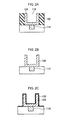
- FIG. 1 is a flowchart describing a method of manufacturing a capacitor according to an embodiment of the present invention
- FIGS. 2A through 2G are cross-sectional views illustrating processes in the method of manufacturing the capacitor according to the embodiment of the present invention.
- FIG. 3 is a cross-sectional view showing another example of the capacitor
- FIG. 4 is a longitudinal sectional view showing an example of a film forming apparatus used to form a dielectric film
- FIG. 5 is a transverse sectional view showing an example of a film forming apparatus used to form a dielectric film
- FIG. 6 is a timing chart showing timings of supplying gases when a first TiO 2 film to and a second TiO 2 film are formed.
- FIG. 7 is a timing chart showing gas supply timing when a ZrO 2 -based film is formed.
- a method of manufacturing a capacitor according to an embodiment of the present invention will be described below.
- a cylinder type capacitor is exemplary shown.
- FIG. 1 is a flowchart describing a method of manufacturing a capacitor according to an embodiment of the present invention
- FIGS. 2A through 2G are cross-sectional views showing processes for manufacturing the capacitor.
- a semiconductor wafer W in which a plurality of contacts 114 formed of, for example, Ti are formed to correspond to locations where capacitors will be formed an insulation layer 102 formed of SO 2 or the like is formed, and then, portions of the insulation layer 102 , which correspond to the contacts 114 , are removed by an etching process to form recess portions 116 of high aspect ratio.
- a lower electrode layer 104 is formed on a surface of the structure which is formed by the above processes to electrically connect to the contacts 114 , and an entire surface is polished by, for example, a chemical mechanical polishing (CMP) method, so that the lower electrode layer 104 only remains on inner walls of the concave portions 116 (operation 1 , FIG. 2A ).
- CMP chemical mechanical polishing
- the lower electrode layer 104 is typically formed as a TiN film, and may be formed by a chemical vapor deposition (CVD) method or an atomic layer deposition (ALD) method by using, for example, a TiCl 4 gas as a Ti material gas and using, for example, a NH 3 gas as a nitriding gas.
- CVD chemical vapor deposition
- ALD atomic layer deposition
- the insulation layer 102 is removed by a wet etching process to remain the lower electrode layer 104 of a cylindrical shape (operation 2 , FIG. 2B ).
- a first TiO 2 film 106 is formed on the lower electrode layer 104 of the cylindrical shape (operation 3 , FIG. 2C ).
- the first TiO 2 film 106 is formed to provide an interface control in regard to the lower electrode layer 104 , and restrains leakage current.
- the first TiO 2 film 106 may have a thin thickness of about 0.2 to 1.5 nm. If the thickness is less than about 0.2 nm, it is difficult to form the film, and if the thickness is greater than about 1.5 nm, an equivalent oxide thickness (EOT) or a capacitance equivalent thickness (CET) of the dielectric film is increased too much.
- EOT equivalent oxide thickness
- CET capacitance equivalent thickness
- the thickness of the first TiO 2 film 106 may be about 0.2 to 1.0 nm.
- the first TiO 2 film 106 may be appropriately formed by the CVD method or the ALD method, as will be described later.
- the first TiO 2 film 106 may be doped with Al, Si, Ta, Nb, or the like.
- a ZrO 2 -based film 108 is formed on the first TiO 2 film 106 (operation 4 , FIG. 2D ).
- the ZrO 2 -based film 108 is crystallized through a subsequent annealing process and serves to increase a dielectric constant of a second TiO 2 film 110 formed thereon.
- the ZrO 2 -based film 108 may have a thickness of about 1 to 10 nm. If the thickness is less than about 1 nm, it is difficult to crystallize the ZrO 2 through the annealing, and if the thickness is greater than about 10 nm, the dielectric constant of the dielectric film may be insufficient.
- the thickness of the ZrO 2 — based film 108 may be about 1 to 5 nm.
- the ZrO 2 — based film 108 may be appropriately formed by the CVD method or the ALD method, as will be described later.
- the ZrO 2 -based film 108 may include ZrO 2 alone. ZrO 2 doped with Al, Si, or the like, a ZAZ structure, in which a ZrO 2 film and Al 2 O 3 film are stacked, and a LAZO structure, in which a ZrO 2 film and an Al 2 O 3 film are alternately formed by an ALD method.
- an annealing process for improving crystallization property of the ZrO 2 is performed to the structure in which the ZrO 2 -based film 108 is formed (operation 5 , FIG. 2E ).
- the annealing is preferably performed within a temperature range from about 300° C. to 600° C. If the annealing temperature is less than about 300° C., it is difficult to crystallize the ZrO 2 in the ZrO 2 -based film 108 , and if the annealing temperature is higher than about 600° C., devices that have been formed before forming the capacitor may be thermally affected. More preferably, the annealing may be performed within a temperature range of about 350° C. to 600° C. The annealing may be performed under an oxygen atmosphere using an O 2 gas, an inert gas atmosphere using an N 2 gas, or a reduction atmosphere using an H 2 gas.
- the second TiO 2 film 110 is formed on the ZrO 2 -based film 110 (operation 6 , FIG. 2F ).
- the second TiO 2 film 110 is formed as a main capacity film.
- the second TiO 2 film 110 may be formed by the CVD or ALD method, as will be described later.
- the TiO 2 may have two kinds of crystal structures, that is, anatase type and rutile type.
- the anatase is a low temperature phase and has a relative dielectric constant of about 40
- the rutile is a high temperature phase and has a relative dielectric constant of 80 or greater.
- the anatase of the low temperature phase is grown, and thus. It is difficult to obtain a high dielectric constant.
- the second TiO 2 film 110 formed on the ZrO 2 -based film 108 has the rutile structure. Therefore, the second TiO 2 film 110 has a high dielectric constant, and contributes to a low EOT (low CET). Also, since the second TiO 2 film 110 has the rutile type crystal structure, a leakage current to an upper electrode layer 112 formed on the second TiO 2 film 110 may be reduced.
- the second TiO 2 film 110 may have a film thickness of about 1 to 20 nm. If the film thickness is less than about 1 nm, the leakage current is increased even though the EOT is good. If the film thickness is greater than about 20 nm, the EOT is increased although the leakage current is reduced. More preferably, the film thickness may be about 1 to 10 nm, and most preferably, about 5 to 10 nm.
- the second TiO 2 film 110 may be doped with Al, Si, Ta, Nb, or the like.
- the upper electrode layer 112 is formed on the second TiO 2 film 110 to complete the capacitor (operation 7 , FIG. 2G ).
- the upper electrode layer 112 is typically formed as a TiN film via the CVD method or the ALD method by using, for example, a TiCl 4 gas as a Ti material gas and using, for example, an NH 3 gas as a nitriding gas.
- the capacitor 120 includes the lower electrode layer 104 , the first TiO 2 film 106 , the ZrO 2 -based film 108 that is crystallized by the annealing process, the second TiO 2 film 110 , and the upper electrode layer 112 .
- the first TiO 2 film 106 , the ZrO 2 -based film 108 , and the second TiO 2 film 110 constitute a dielectric film.
- a total thickness of the dielectric film may be about 5 to 25 nm, and more preferably, about 5 to 15 nm.
- the leakage current to the lower electrode layer 104 may be restrained.
- the annealing process for crystallizing the ZrO 2 is performed, and thus, the ZrO 2 of the ZrO 2 -based film 108 may be crystallized, and the second TiO 2 film 110 which is formed on the ZrO 2 -based film 108 and serves as a capacity film can be grown to have the rutile structure. Accordingly, the dielectric constant of the second TiO 2 film 110 can be improved, and the leakage current can be restrained.
- the high dielectric constant property that is, the low EOT (low CET)
- the low leakage current can be compatibly achieved.
- a TiN film that is conventionally used can be used as an electrode material, and a special material or a base layer is not necessary. Thus, there is no difficulty in manufacturing the capacitor.
- the structure of the capacitor is not limited to the cylinder type, but may be formed as various types.
- the capacitor may have a filler type structure that is more advantageous for the fine structure.
- a filler type capacitor 120 ′ is fabricated by forming the first TiO 2 film 106 on a filler-shaped lower electrode layer 104 ′, forming the ZrO 2 -based film 108 , crystallizing the ZrO 2 of the ZrO 2 -based film 108 through the annealing process, forming the second TiO 2 film 110 , and forming the upper electrode layer 112 , in the same order as that of manufacturing the above capacitor 120 .
- FIG. 4 is a longitudinal sectional view of an example of a film forming apparatus 100 for forming the dielectric film
- FIG. 5 is a transverse sectional view of the film forming apparatus 100 of FIG. 4 .
- a heating apparatus is omitted.
- the film forming apparatus 100 includes a processing chamber 1 formed as a cylinder having opened lower end and a ceiling.
- the processing chamber 1 may be entirely formed of, for example, quartz
- a ceiling plate 2 formed of quartz is provided and sealed on the ceiling in the processing chamber 1 .
- a manifold 3 formed of, for example, a stainless steel cylinder, is connected to the lower opening of the processing chamber 1 via a sealing member 104 such as an O-ring.
- the manifold 3 supports a lower portion of the processing container 1 .
- a wafer boat 5 that is formed of quartz and holds a plurality of semiconductor wafers W (hereinafter, referred to as wafers) as processing targets, for example, about 50 to 100 semiconductor wafers W, in multiple stages is configured to be inserted into the processing container 1 from a lower portion of the manifold 3 .
- the wafer boat 5 includes three pillars 6 (refer to FIG. 5 ), and the plurality of wafers W are supported by grooves formed in the pillars 6 .
- the wafer boat 5 is placed on a table 8 via a thermos tube 7 formed of quartz.
- the table 8 is supported on a rotary shaft 10 that penetrates through a cover unit 9 which opens/closes the lower opening of the manifold 3 and is formed of, for example, stainless steel.
- a magnetic fluid seal 11 for example, is provided on a penetration portion of the rotary shaft 10 so as to airtightly seal and rotatably support the rotary shaft 10 ,
- the rotary shaft 10 is attached to a leading edge of an arm 13 supported by an elevation mechanism (not shown), for example, a boat elevator, so that the wafer boat 5 , the cover unit 9 , and the like are integrally elevated to be inserted into/withdrawn from the processing chamber 1 . Otherwise, the table 8 is fixedly formed at the cover unit 9 so as to perform processes of the wafers W without rotating the wafer boat 5 .
- an elevation mechanism for example, a boat elevator
- the film forming apparatus 100 includes an oxidizing agent supply mechanism 14 for supplying a oxidizing agent gas, for example, an O 3 gas, into the processing chamber 1 , a Zr source gas supply mechanism 15 for supplying a Zr source gas (Zr material gas) into the processing chamber 1 , and a Ti source gas supply mechanism 16 for supplying a Ti source gas (Ti material gas) into the processing chamber 1 . Also, the film forming apparatus 100 also includes a purge gas supply mechanism 30 for supplying an inert gas, for example, an N 2 gas, as a purge gas into the processing chamber 1 .
- a purge gas supply mechanism 30 for supplying an inert gas, for example, an N 2 gas, as a purge gas into the processing chamber 1 .
- the oxidizing agent supply mechanism 14 includes an oxidizing agent supply source 17 , an oxidizing agent pipe 18 for inducing the oxidizing agent from the oxidizing agent supply source 17 , and an oxidizing agent diffusion nozzle 19 which is connected to the oxidizing agent pipe 18 , is formed of a quartz pipe, penetrates into the manifold 3 through a side wall of the manifold 3 , bends upward and extends perpendicularly.
- a plurality of gas ejection holes 19 a are formed in the oxidizing agent diffusion nozzle 19 at predetermined intervals at the perpendicular portion of the oxidizing agent diffusion nozzle 19 , so that the oxidizing agent, for example, the O 3 gas, may be evenly discharged from the gas ejection holes 19 a toward the processing chamber 1 in a horizontal direction.
- An H 2 O gas, an O 2 gas, an NO 2 gas, an NO gas, and an N 2 O gas may be used as the oxidizing agent, in addition to the above O 3 gas.
- a plasma generation mechanism may be provided to plasmatize the oxidizing agent so as to improve reactivity.
- an O 2 gas and an H 2 gas may be used to cause radical oxidation.
- an ozonizer generating the O 3 gas is used as the oxidizing agent supply source 17 .
- the Zr source gas supply mechanism 15 includes a Zr source storage container 20 in which Zr source formed of a Zr compound is stored, a Zr source pipe 21 for inducing liquid Zr source from the Zr source storage container 20 , a vaporizer 22 connected to the Zr source pipe 21 for vaporizing the Zr source, a Zr source gas pipe 23 for inducing a Zr source gas generated by the vaporizer 22 , and a Zr source gas diffusion nozzle 24 which is formed of quartz pipe, is connected to the Zr source gas pipe 23 , penetrates into the manifold 3 through a side wall of the manifold 3 , bends upward and extends perpendicularly.
- a carrier gas pipe 22 a for supplying an N 2 gas as a carrier gas is connected to the vaporizer 22 .
- a plurality of gas ejection holes 24 a are formed in the Zr source gas diffusion nozzle 24 at predetermined intervals in a length direction of the Zr source gas diffusion nozzle 24 , so that the Zr source gas may be evenly discharged from the gas ejection holes 24 a in a horizontal direction.
- a Zr compound including a cyclopentadienyl ring such as cyclopentadienyl tris(dimethylamino)zirconium (ZrCp(NMe 2 ) 3 ; CPDTMZ), methycyclopentadienyl tris(dimethylamino)zirconium (Zr(MeCp)(NMe 2 ) 3 ; MCPDTMZ), and the like may be appropriately used.
- the Ti source gas supply mechanism 16 includes a Ti source storage container 25 in which a Ti source formed of a Ti compound is stored, a Ti source pipe 26 for inducing a liquid state Ti source from the Ti source storage container 25 , a vaporizer 27 connected to the Ti source pipe 26 to vaporize the Ti source, a Ti source gas pipe 28 for inducing a Ti source gas generated by the vaporizer 27 , and a Ti source gas diffusion nozzle 29 which is formed of a quartz pipe, is connected to the Ti source gas pipe 28 , penetrates into the manifold 3 through a side wall of the manifold 3 , bends upward and extends perpendicularly.
- a carrier gas pipe 27 a for supplying an N 2 gas as a carrier gas is connected to the vaporizer 27 .
- a plurality of gas ejection holes 29 a are formed in the Ti source gas diffusion nozzle 29 at predetermined intervals in a length direction of the Ti source gas diffusion nozzle 29 , so that the Ti source gas may be evenly discharged from the gas ejection holes 29 a into the processing chamber 1 in a horizontal direction.
- Ti compound for example, a compound including a cyclopentadienyl ring, such as methycyclopentadienyl tris(dimethylamino)titanium (Ti(MeCp)(NMe 2 ) 3 ; MCPDTMT) may be appropriately used.
- a compound including a cyclopentadienyl ring such as methycyclopentadienyl tris(dimethylamino)titanium (Ti(MeCp)(NMe 2 ) 3 ; MCPDTMT) may be appropriately used.
- the purge gas supply mechanism 30 includes a purge gas supply source 31 , a purge gas pipe 32 for inducing a purge gas from the purge gas supply source 31 , and a purge gas nozzle 33 connected to the purge gas pipe 32 and penetrating a side wall of the manifold 3 .
- An inert gas for example, an N 2 gas, may be used as the purge gas.
- An opening/closing valve 18 a and a flow controller 18 b such as a mass flow controller are provided in the oxidizing agent pipe 18 so that the oxidizing agent gas can be supplied while controlling a flow rate thereof.
- an opening/closing valve 32 a and a flow controller 32 b such as a mass flow controller are provided in the purge gas pipe 32 so that the purge gas can be supplied while controlling a flow rate thereof.
- a Zr source pressure feed pipe 20 a is inserted in the Zr source storage container 20 , and the liquid type Zr source is fed into the Zr source pipe 21 by supplying a pressure feed gas such as a He gas from the Zr source pressure feed pipe 20 a .
- a flow controller 21 a such as a liquid mass flow controller is provided in the Zr source pipe 21 , and a valve 23 a is provided in the Zr source gas pipe 23 .
- a Ti source pressure feed pipe 25 a is inserted in the Ti source storage container 25 , and the Ti source liquid is fed into the Ti source pipe 26 by supplying a pressure feed gas such as a He gas from the Ti source pressure feed pipe 25 a .
- a flow controller 26 a such as a liquid mass flow controller is provided in the Ti source pipe 26 , and a valve 28 a is provided in the Ti source gas pipe 28 .
- the oxidizing agent diffusion nozzle 19 for discharging the oxidizing agent is provided in a recess portion 1 a of the processing chamber 1 , and the Zr source gas diffusion nozzle 24 and the Ti source gas diffusion nozzle 29 are provided so that the oxidizing agent diffusion nozzle 19 can be interposed therebetween.
- An exhaust hole 37 for vacuum exhausting the processing chamber 1 is formed at a side opposite to the oxidizing agent diffusion nozzle 19 , the Zr source gas diffusion nozzle 24 , and the Ti source gas diffusion nozzle 29 in the processing chamber 1 .
- the exhaust hole 37 is formed thin and long by shaving off the side wall of the processing chamber 1 in an up-and-down direction.
- An exhaust hole cover member 38 having a U-shaped cross-section to cover the exhaust hole 37 is welded and attached to a portion which corresponds to the exhaust hole 37 in the processing chamber 1 .
- the exhaust hole cover member 38 extends upward along the side wall of the processing chamber 1 , and defines a gas outlet 39 at an upper portion of the processing chamber 1 .
- a vacuum exhaustion mechanism (not shown) which includes a vacuum pump and the like and performs vacuum suction is provided to the gas outlet 39 .
- the ZrO 2 -based film may be doped with Al, Si, or the like, and may have the ZAZ structure or the LAZO structure, and the first and second TiO 2 films may be doped with Al, Si, Ta, Nb, and the like.
- a supply mechanism for supplying a material of doped element or a material of Al when forming the ZAZ structure or the LAZO structure may be additionally provided.
- Control of each of the components of the film forming apparatus 100 for example, supplying and stopping of each gas by opening/closing the opening/closing valves 18 a , 23 a , 28 a , and 32 a , controlling of the flow rate of the gas or the liquid source by using the flow controller 18 b , 21 a , 26 a , and 32 b , switching of the gas introduced in the processing chamber 1 , controlling of the heating unit 40 , and the like are performed by a controller 50 formed of, for example, a micro processor (computer).
- a user interface 51 including a keyboard that receives an input operation of a command or the like for an operator to control the film forming apparatus 100 or a display that visibly displays an operating state of the film forming apparatus 100 is connected to the controller 50 .
- a memory unit 52 for storing a controlling program for performing the various processes performed in the film forming apparatus 100 under a control of the controller 50 or storing a program for performing a process in each of components of the film forming apparatus 100 according to processing condition, that is, a recipe, is connected to the controller 50 .
- the recipe is recorded in a recording medium of the memory unit 52 .
- the recording medium may be a fixed unit such as a hard disk, or a portable unit such as a CD-ROM, a DVD, a flash memory, or the like.
- the recipe may be appropriately transferred from another device via, for example, an exclusive line.
- a certain recipe is called out of the memory unit 52 by a command or the like from the user interface 51 , and executed in the controller 50 , and thus a predetermined process in the film forming apparatus 100 is performed under the control of the controller 50 .
- the recording medium of the memory unit 52 stores a program (that is, a processing recipe) for executing a film forming method that will be described below, and the program controls the film forming apparatus 100 to make the controller 50 execute the film forming method of the dielectric film that will be described below.
- the wafer boat 5 on which a plurality of, for example, about 50 to 100, wafers W are placed under room temperature is elevated to be loaded in the processing chamber 1 at a predetermined temperature from a lower portion of the processing chamber 1 , and the cover unit 9 closes the lower opening of the manifold 3 to seal the processing chamber 1 .
- the inside of the processing chamber 1 is maintained at predetermined processing pressure by performing a vacuum suction of the inside of the processing chamber 1 , and at the same time, a power supply to the heating unit 40 is controlled to increase the temperature of the wafers W to maintain the processing temperature. Then, a film forming process begins in a state where the wafer boat 5 is rotated.
- the first TiO 2 film is formed by using the above described Ti source gas formed of the Ti compound and the oxidizing agent, while the heating unit 40 heats the so processing chamber 1 to a temperature of about 200 to 300° C.
- the heating unit 40 heats the so processing chamber 1 to a temperature of about 200 to 300° C.
- a TiO 2 film having a predetermined film thickness is formed by performing, repeatedly and a plurality of times, a cycle of TiO 2 film forming operation via the ALD method, herein a cycle of TiO 2 film forming operation includes a step S 1 for supplying the Ti source gas to the processing chamber 1 to be adsorbed on a ZrO 2 film, a step S 2 for purging the inside of the processing chamber 1 by using a purge gas, a step S 3 for supplying a oxidizing agent gas, for example, an O 3 gas, to the processing chamber 1 to oxidize the Ti source gas, and a step S 4 for purging the inside of the processing chamber 1 with the purge gas.
- a cycle of TiO 2 film forming operation includes a step S 1 for supplying the Ti source gas to the processing chamber 1 to be adsorbed on a ZrO 2 film, a step S 2 for purging the inside of the processing chamber 1 by using a purge gas, a step S 3 for supplying a oxidizing agent
- the first TiO 2 film can be doped with the Al, Si, Ta, Nb, and the like, and in this case, a step of supplying a material of the element by the number of times according to a doped amount may be inserted in the repeated cycle.
- the Ti source storage container 25 of the Ti source gas supply mechanism 16 supplies the Ti compound that is the Ti source, the vaporizer 27 vaporizes the Ti compound to generate the Ti source gas, and the Ti source gas is supplied to the processing chamber 1 for a time period of T 1 from the gas ejection holes 29 a via the Ti source gas pipe 28 and the Ti source gas diffusion nozzle 29 . Accordingly, the Ti source gas is adsorbed on the lower electrode.
- the time period T 1 of the step S 1 may be, for example, about 0.1 to 1800 sec.
- a flow rate of the Ti source may be, for example, about 0.01 to 10 ml/min (ccm).
- a pressure in the processing chamber 1 may be, for example, about 0.3 to 66650 Pa.
- the oxidizing agent for example, the O 3 gas
- the oxidizing agent supply source 17 of the oxidizing agent supply mechanism 14 via the oxidizing agent pipe 18 and the oxidizing agent diffusion nozzle 19 . Accordingly, the Ti source adsorbed on the lower electrode is oxidized to form the TiO 2 film.
- a time period T 3 of the step S 3 may be within a range of about 0.1 to 1800 sec.
- a flow rate of the oxidizing agent may vary depending on the number of loaded wafers W or a kind of the oxidizing agent; however, when the O 3 gas is used as the oxidizing agent gas and the number of loaded wafers W is about 50 to 100, the flow rate of the oxidizing agent may be, for example, about 1 to 500 g/Nm 3 .
- the pressure in the processing chamber 1 may be, for example, about 0.3 to 66650 Pa.
- the steps S 2 and S 4 are performed to remove remaining gas in the processing chamber 1 after the step S 1 and step S 3 , so as to generate a desired reaction in a next step.
- the purge gas for example, an N 2 gas
- the purge gas supply source 31 of the purge gas supply mechanism 30 is supplied to the processing chamber 1 from the purge gas supply source 31 of the purge gas supply mechanism 30 via the purge gas pipe 32 and the purge gas nozzle 33 , so as to purge the inside of the processing chamber 1 .
- the vacuum suction and the supply of the purge gas are performed repeatedly to improve an efficiency of removing the remaining gas.
- Time periods T 2 and T 4 for performing the step S 2 and S 4 may be, for example, about 0.1 to 1800 sec.
- the pressure in the processing chamber 1 may be, for example, about 0.3 to 66650 Pa.
- a time for vacuum suction and a time for supplying the purge gas may be switched due to a difference of properties of the gas discharge. In particular, it takes longer to discharge the gas after performing the step S 1 than after the step S 3 and accordingly the time for performing the step S 2 after the step S 1 may be increased.
- the ZrO 2 -based film is formed by using the above described Zr source gas formed of the Zr compound and the oxidizing agent, while heating the inside the processing chamber 1 to a temperature of about 200 to 300° C. by using the heating unit 40 .
- a timing chart of FIG. 1 As shown in a timing chart of FIG.
- a ZrO 2 -based film having a predetermined film thickness is formed by performing, repeatedly and a plurality of times, a cycle of ZrO 2 film forming operation via the ALD method, herein the cycle of ZrO 2 film forming operation includes a step S 11 for supplying the Zr source gas to the processing chamber 1 to be adsorbed on the first TiO 2 film, a step S 12 for purging the inside of the processing chamber 1 by using a purge gas, a step S 13 for supplying a oxidizing agent gas, for example, an O 3 gas, to the processing chamber 1 to oxidize the Zr source gas, and a step S 14 for purging the inside of the processing chamber 1 with the purge gas.
- the cycle of ZrO 2 film forming operation includes a step S 11 for supplying the Zr source gas to the processing chamber 1 to be adsorbed on the first TiO 2 film, a step S 12 for purging the inside of the processing chamber 1 by using a purge gas, a step S 13 for supplying
- the ZrO 2 -based film may be doped with the Al, Si, or the like, or may have the ZAZ structure and the LAZO structure, and in this case, following operation may be performed.
- a step of supplying a material of the element may be inserted in the cycle of the steps S 11 through S 14 , by the number of times according to the doped amount.
- an Al compound supply mechanism is additionally provided, and then, a ZrO 2 film of a predetermined film thickness is formed by using the ALD operation for a predetermined times, an Al 2 O 5 film is formed by the same ALD operation, and additionally, a ZrO 2 film is formed by the ALD method.
- the Al compound supply mechanism is additionally provided as described above, and then, a Zr source gas supplying step, an oxidizing step, an Ar source gas supplying step, and an oxidizing step are alternately and repeatedly performed.
- the Zr source storage container 20 of the Zr source gas supply mechanism 15 supplies the Zr compound that is the Zr source, the vaporizer 22 vaporizes the Zr compound to generate the Zr source gas, and the Zr source gas is supplied to the processing chamber 1 for a time period of T 1 from the gas ejection holes 24 a via the Zr source gas pipe 23 and the Zr source gas diffusion nozzle 24 . Accordingly, the Zr source gas is adsorbed on the wafer W.
- the time period T 1 of the step S 11 may be, for example, about 0.1 to 1800 sec.
- a flow rate of the Zr source may be, for example, about 0.01 to 10 ml/min (ccm).
- a pressure in the processing chamber 1 may be, for example, about 0.3 to 66650 Pa.
- the step S 13 for supplying the oxidizing agent, and the steps S 12 and S 14 for purging are performed in the same manner as the step S 3 for supplying the oxidizing agent and the purging steps S 2 and S 4 when forming the first TiO 2 film.
- Time periods T 13 , T 12 , and T 14 are the same as T 3 , T 2 , and T 4 .
- the annealing process is performed for a predetermined time after finishing the forming of the ZrO 2 -based film, in a state where the pressure in the processing chamber 1 becomes a decompression state of a predetermined pressure while introducing a predetermined atmospheric gas to the processing chamber 1 and the heating unit 40 heats the processing chamber 1 to a temperature of about 300 to 600° C., as described above. If the annealing process is performed under an inert environment, the N 2 gas, i.e., may be introduced to the processing chamber 1 from the purge gas supply source 31 .
- the oxidizing agent may be introduced to the processing chamber 1 from the oxidizing agent supply source 17 or an O 2 gas may be introduced from O 2 gas introduction mechanism which is additionally provided. Also, if the annealing process is performed under a reduction environment, a mechanism for introducing a reducing gas such as an H 2 gas may be additionally provided.
- the second TiO 2 film can be formed by using the Ti source gas formed of the Ti compound and the oxidizing agent, according to the ALD method shown in the timing chart of FIG. 6 .
- the second TiO 2 film can be doped with the Al, Si, Ta, Nb, and the like, and in this case, a step of supplying a material of the element by a number of times according to a doped amount may be inserted in the repeated cycle.
- the first and second TiO 2 films are formed by using the Ti source gas and the oxidizing agent via the ALD method, and the ZrO 2 -based film is formed by using the Zr source gas and the oxidizing gas via the ALD method, and thus, a film having less impurities and defects may be obtained under a relatively low temperature.
- a compound containing the cyclopentadienyl ring is used as the Ti source gas and the Zr source gas, an side opposite to the cyclopentadienyl ring becomes an adsorption site, and thereby performing the adsorbing and arranging regularly and obtaining a dense film having less impurities and defects.
- a first TiO 2 film was formed to a thickness of about 1 nm
- a ZrO 2 film was formed on the first TiO 2 film to a thickness of about 5 nm
- an annealing was performed at a temperature of about 500° C. for about 10 minutes under an N 2 gas environment
- a second TiO 2 film was formed on the ZrO 2 film to a thickness of about 5 nm, thereby forming a dielectric film having a total thickness of about 11 nm.
- a TiN film as an upper electrode was formed on the second TiO 2 film to manufacture a flat capacitor sample.
- the first and second TiO 2 films were formed by using an MCPDTMT as the Ti source and the O 3 gas as the oxidizing agent in the ALD method having the sequences shown in the timing chart of FIG. 6 by the film forming apparatus 100 shown in FIG. 4 .
- the ZrO 2 film was formed by using a CPDTMZ as the Zr source and the O 3 gas as the oxidizing agent in the ALD method having the sequences shown in the timing chart of FIG. 7 by the film forming apparatus shown in FIG. 4 .
- the present invention may be variously modified without limiting to the above embodiments.
- the first and second TiO 2 films and the ZrO 2 -based film are formed by using the ALD method; however, the present invention is not limited thereto, and the above films may be formed by using the CVD method.
- the forming of the first and second TiO 2 films and the ZrO 2 -based film are formed by a batch-type film forming apparatus, in which the film forming operations are performed in a lump with respect to a plurality of wafers W loaded therein; however, the present invention is not limited thereto, and may be applied to a single-wafer type film forming apparatus which performs the film forming operation on one wafer at a time.
- the first TiO 2 film is formed on the lower electrode for interface control, and thus, the leakage current to the lower electrode may be restrained. Also, after forming the ZrO 2 -based film on the first TiO 2 film, the annealing process for crystallizing the ZrO 2 is performed, and thus, the ZrO 2 in the ZrO 2 -based film can be crystallized. Thus, the second TiO 2 film formed on the ZrO 2 -based film and serving as a capacity film can be grown to have the rutile structure. Accordingly, the dielectric constant of the second TiO 2 film is increased, and the leakage current to the upper electrode can be also restrained.
- the high dielectric constant property and the low leakage current can be achieved compatibly.
- the TiN film that is conventionally used can be used as the electrode material, and thus, a unique electrode material or a base is not necessary, and there is no difficulty in fabricating the capacitor.
Applications Claiming Priority (2)
| Application Number | Priority Date | Filing Date | Title |
|---|---|---|---|
| JP2012-023469 | 2012-02-06 | ||
| JP2012023469A JP5882075B2 (ja) | 2012-02-06 | 2012-02-06 | キャパシタの製造方法、キャパシタ、およびそれに用いられる誘電体膜の形成方法 |
Publications (2)
| Publication Number | Publication Date |
|---|---|
| US20130200491A1 US20130200491A1 (en) | 2013-08-08 |
| US8896097B2 true US8896097B2 (en) | 2014-11-25 |
Family
ID=48902192
Family Applications (1)
| Application Number | Title | Priority Date | Filing Date |
|---|---|---|---|
| US13/760,210 Active 2033-03-07 US8896097B2 (en) | 2012-02-06 | 2013-02-06 | Method of manufacturing capacitor, capacitor and method of forming dielectric film for use in capacitor |
Country Status (4)
| Country | Link |
|---|---|
| US (1) | US8896097B2 (zh) |
| JP (1) | JP5882075B2 (zh) |
| KR (1) | KR101609182B1 (zh) |
| TW (1) | TWI536453B (zh) |
Cited By (7)
| Publication number | Priority date | Publication date | Assignee | Title |
|---|---|---|---|---|
| US20140175422A1 (en) * | 2012-12-20 | 2014-06-26 | Intermolecular, Inc. | Deposition of Rutile Films with Very High Dielectric Constant |
| US9978753B2 (en) | 2016-06-02 | 2018-05-22 | Samsung Electronics Co., Ltd. | Semiconductor device and method of manufacturing the same |
| US10453913B2 (en) | 2017-04-26 | 2019-10-22 | Samsung Electronics Co., Ltd. | Capacitor, semiconductor device and methods of manufacturing the capacitor and the semiconductor device |
| US10593777B2 (en) | 2018-07-13 | 2020-03-17 | SK Hynix Inc. | Semiconductor device and method for fabricating the same |
| US10964614B2 (en) | 2018-09-28 | 2021-03-30 | SK Hynix Inc. | Semiconductor device and method for fabricating the same |
| US11133314B2 (en) | 2019-11-01 | 2021-09-28 | Samsung Electronics Co., Ltd. | Semiconductor memory device and method of fabricating the same |
| US11227912B2 (en) | 2019-06-11 | 2022-01-18 | Samsung Electronics Co., Ltd. | Integrated circuit device and method of manufacturing the same |
Families Citing this family (10)
| Publication number | Priority date | Publication date | Assignee | Title |
|---|---|---|---|---|
| US9105646B2 (en) * | 2012-12-31 | 2015-08-11 | Intermolecular, Inc. | Methods for reproducible flash layer deposition |
| DE102013109357A1 (de) * | 2013-08-29 | 2015-03-05 | Endress + Hauser Conducta Gesellschaft für Mess- und Regeltechnik mbH + Co. KG | Ionensensitive Schichtstruktur für einen ionensensitiven Sensor und Verfahren zur Herstellung derselben |
| JP6616070B2 (ja) * | 2013-12-01 | 2019-12-04 | ユージェヌス インコーポレイテッド | 誘電性複合体構造の作製方法及び装置 |
| JP2015188028A (ja) * | 2014-03-27 | 2015-10-29 | 東京エレクトロン株式会社 | 薄膜形成方法、及び、薄膜形成装置 |
| JP6458595B2 (ja) | 2015-03-27 | 2019-01-30 | 東京エレクトロン株式会社 | 成膜装置及び成膜方法並びに記憶媒体 |
| KR102350589B1 (ko) * | 2015-08-24 | 2022-01-14 | 삼성전자주식회사 | 박막 형성 방법 및 이를 이용한 집적회로 소자의 제조 방법 |
| TWI661076B (zh) * | 2016-10-06 | 2019-06-01 | 南韓商圓益Ips股份有限公司 | 複合膜製造方法 |
| US20180061608A1 (en) * | 2017-09-28 | 2018-03-01 | Oxford Instruments X-ray Technology Inc. | Window member for an x-ray device |
| US11688601B2 (en) * | 2020-11-30 | 2023-06-27 | International Business Machines Corporation | Obtaining a clean nitride surface by annealing |
| TW202247412A (zh) * | 2021-02-08 | 2022-12-01 | 日商東京威力科創股份有限公司 | 基板處理方法及基板處理裝置 |
Citations (14)
| Publication number | Priority date | Publication date | Assignee | Title |
|---|---|---|---|---|
| JP2001152339A (ja) | 1999-10-06 | 2001-06-05 | Samsung Electronics Co Ltd | 原子層蒸着法を用いた薄膜形成方法 |
| US6288420B1 (en) * | 1999-05-21 | 2001-09-11 | Sharp Laboratories Of America, Inc. | Composite iridium-metal-oxygen barrier structure with refractory metal companion barrier |
| US6365123B1 (en) * | 1998-12-18 | 2002-04-02 | Ford Global Technologies, Inc. | Sol-gel processed metal-zirconia materials |
| US6445033B1 (en) * | 1999-06-30 | 2002-09-03 | Nec Corporation | Gate-insulating film including oxide film |
| US6803635B2 (en) * | 2001-04-13 | 2004-10-12 | Kabushiki Kaisha Toshiba | MIS field effect transistor with metal oxynitride film |
| JP2004296814A (ja) | 2003-03-27 | 2004-10-21 | Elpida Memory Inc | 金属酸化膜の形成方法 |
| US20070102742A1 (en) * | 2005-11-10 | 2007-05-10 | Hynix Semiconductor Inc. | Capacitor and method for fabricating the same |
| US7309616B2 (en) * | 2003-03-13 | 2007-12-18 | Unity Semiconductor Corporation | Laser annealing of complex metal oxides (CMO) memory materials for non-volatile memory integrated circuits |
| JP2008181943A (ja) | 2007-01-23 | 2008-08-07 | Fujikura Ltd | ファイバ・パルスレーザ装置及びその制御方法 |
| US7473565B2 (en) * | 2002-05-28 | 2009-01-06 | Kabushiki Kaisha Toshiba | Semiconductor device and method of manufacturing the same |
| US7476916B2 (en) * | 2003-05-29 | 2009-01-13 | Nec Corporation | Semiconductor device having a mis-type fet, and methods for manufacturing the same and forming a metal oxide film |
| JP2009293302A (ja) | 2008-06-06 | 2009-12-17 | World Garage Door:Kk | 可動式間仕切り及び可動式間仕切り組立体 |
| WO2010082605A1 (ja) | 2009-01-15 | 2010-07-22 | 東京エレクトロン株式会社 | キャパシタ及びキャパシタの製造方法 |
| US20110018100A1 (en) * | 2008-03-28 | 2011-01-27 | Takashi Nakagawa | Capacitor, semiconductor device comprising the same, method for manufacturing the capacitor, and method for manufacturing the semiconductor device |
Family Cites Families (5)
| Publication number | Priority date | Publication date | Assignee | Title |
|---|---|---|---|---|
| TW476128B (en) * | 1999-09-24 | 2002-02-11 | Applied Materials Inc | Integrated method and apparatus for forming an enhanced capacitor |
| JP4792132B2 (ja) * | 2009-02-27 | 2011-10-12 | キヤノンアネルバ株式会社 | 誘電体ならびに半導体装置の製造方法、プログラム、および、記録媒体 |
| JP5647792B2 (ja) * | 2009-04-01 | 2015-01-07 | ピーエスフォー ルクスコ エスエイアールエルPS4 Luxco S.a.r.l. | キャパシタ用容量絶縁膜の製造方法 |
| JP2011222699A (ja) * | 2010-04-08 | 2011-11-04 | Elpida Memory Inc | 半導体用配線 |
| JP5576719B2 (ja) * | 2010-06-10 | 2014-08-20 | ルネサスエレクトロニクス株式会社 | 半導体装置の製造方法 |
-
2012
- 2012-02-06 JP JP2012023469A patent/JP5882075B2/ja active Active
-
2013
- 2013-01-31 KR KR1020130010761A patent/KR101609182B1/ko active IP Right Grant
- 2013-02-01 TW TW102104024A patent/TWI536453B/zh active
- 2013-02-06 US US13/760,210 patent/US8896097B2/en active Active
Patent Citations (14)
| Publication number | Priority date | Publication date | Assignee | Title |
|---|---|---|---|---|
| US6365123B1 (en) * | 1998-12-18 | 2002-04-02 | Ford Global Technologies, Inc. | Sol-gel processed metal-zirconia materials |
| US6288420B1 (en) * | 1999-05-21 | 2001-09-11 | Sharp Laboratories Of America, Inc. | Composite iridium-metal-oxygen barrier structure with refractory metal companion barrier |
| US6445033B1 (en) * | 1999-06-30 | 2002-09-03 | Nec Corporation | Gate-insulating film including oxide film |
| JP2001152339A (ja) | 1999-10-06 | 2001-06-05 | Samsung Electronics Co Ltd | 原子層蒸着法を用いた薄膜形成方法 |
| US6803635B2 (en) * | 2001-04-13 | 2004-10-12 | Kabushiki Kaisha Toshiba | MIS field effect transistor with metal oxynitride film |
| US7473565B2 (en) * | 2002-05-28 | 2009-01-06 | Kabushiki Kaisha Toshiba | Semiconductor device and method of manufacturing the same |
| US7309616B2 (en) * | 2003-03-13 | 2007-12-18 | Unity Semiconductor Corporation | Laser annealing of complex metal oxides (CMO) memory materials for non-volatile memory integrated circuits |
| JP2004296814A (ja) | 2003-03-27 | 2004-10-21 | Elpida Memory Inc | 金属酸化膜の形成方法 |
| US7476916B2 (en) * | 2003-05-29 | 2009-01-13 | Nec Corporation | Semiconductor device having a mis-type fet, and methods for manufacturing the same and forming a metal oxide film |
| US20070102742A1 (en) * | 2005-11-10 | 2007-05-10 | Hynix Semiconductor Inc. | Capacitor and method for fabricating the same |
| JP2008181943A (ja) | 2007-01-23 | 2008-08-07 | Fujikura Ltd | ファイバ・パルスレーザ装置及びその制御方法 |
| US20110018100A1 (en) * | 2008-03-28 | 2011-01-27 | Takashi Nakagawa | Capacitor, semiconductor device comprising the same, method for manufacturing the capacitor, and method for manufacturing the semiconductor device |
| JP2009293302A (ja) | 2008-06-06 | 2009-12-17 | World Garage Door:Kk | 可動式間仕切り及び可動式間仕切り組立体 |
| WO2010082605A1 (ja) | 2009-01-15 | 2010-07-22 | 東京エレクトロン株式会社 | キャパシタ及びキャパシタの製造方法 |
Cited By (13)
| Publication number | Priority date | Publication date | Assignee | Title |
|---|---|---|---|---|
| US20140175422A1 (en) * | 2012-12-20 | 2014-06-26 | Intermolecular, Inc. | Deposition of Rutile Films with Very High Dielectric Constant |
| US9222170B2 (en) * | 2012-12-20 | 2015-12-29 | Intermolecular, Inc. | Deposition of rutile films with very high dielectric constant |
| US10636795B2 (en) | 2016-06-02 | 2020-04-28 | Samsung Electronics Co., Ltd. | Semiconductor device and method of manufacturing the same |
| US10297600B2 (en) | 2016-06-02 | 2019-05-21 | Samsung Electronics Co., Ltd. | Semiconductor device and method of manufacturing the same |
| US9978753B2 (en) | 2016-06-02 | 2018-05-22 | Samsung Electronics Co., Ltd. | Semiconductor device and method of manufacturing the same |
| US11177263B2 (en) | 2016-06-02 | 2021-11-16 | Samsung Electronics Co., Ltd. | Semiconductor device and method of manufacturing the same |
| US10453913B2 (en) | 2017-04-26 | 2019-10-22 | Samsung Electronics Co., Ltd. | Capacitor, semiconductor device and methods of manufacturing the capacitor and the semiconductor device |
| US10658454B2 (en) | 2017-04-26 | 2020-05-19 | Samsung Electronics Co., Ltd. | Capacitor, semiconductor device and methods of manufacturing the capacitor and the semiconductor device |
| US10593777B2 (en) | 2018-07-13 | 2020-03-17 | SK Hynix Inc. | Semiconductor device and method for fabricating the same |
| US10964614B2 (en) | 2018-09-28 | 2021-03-30 | SK Hynix Inc. | Semiconductor device and method for fabricating the same |
| US11227912B2 (en) | 2019-06-11 | 2022-01-18 | Samsung Electronics Co., Ltd. | Integrated circuit device and method of manufacturing the same |
| US11133314B2 (en) | 2019-11-01 | 2021-09-28 | Samsung Electronics Co., Ltd. | Semiconductor memory device and method of fabricating the same |
| US11600621B2 (en) | 2019-11-01 | 2023-03-07 | Samsung Electronics Co., Ltd. | Semiconductor memory device and method of fabricating the same |
Also Published As
| Publication number | Publication date |
|---|---|
| KR20130090808A (ko) | 2013-08-14 |
| TW201342474A (zh) | 2013-10-16 |
| TWI536453B (zh) | 2016-06-01 |
| KR101609182B1 (ko) | 2016-04-05 |
| US20130200491A1 (en) | 2013-08-08 |
| JP5882075B2 (ja) | 2016-03-09 |
| JP2013161988A (ja) | 2013-08-19 |
Similar Documents
| Publication | Publication Date | Title |
|---|---|---|
| US8896097B2 (en) | Method of manufacturing capacitor, capacitor and method of forming dielectric film for use in capacitor | |
| US20150221529A1 (en) | Gas supply method and thermal treatment method | |
| JP5097554B2 (ja) | 半導体装置の製造方法、基板処理方法および基板処理装置 | |
| JP5661262B2 (ja) | 成膜方法および成膜装置 | |
| US20120280369A1 (en) | Method for manufacturing semiconductor device, substrate processing apparatus, and semiconductor device | |
| KR101552856B1 (ko) | 성막 방법 및 성막 장치 | |
| JP2011049531A (ja) | 半導体デバイスの製造方法、半導体デバイス及び基板処理装置 | |
| JP5221089B2 (ja) | 成膜方法、成膜装置および記憶媒体 | |
| JP5678252B2 (ja) | Sr−Ti−O系膜の成膜方法 | |
| WO2012090831A1 (ja) | 半導体デバイスの製造方法および基板処理装置 | |
| JP5248025B2 (ja) | SrTiO3膜の成膜方法およびコンピュータ読取可能な記憶媒体 | |
| TWI405264B (zh) | 金屬氧化物膜之形成 | |
| JP5751754B2 (ja) | 成膜方法および記憶媒体 | |
| KR101501803B1 (ko) | 성막 방법, 성막 장치 및 기억 매체 | |
| JP2012134311A (ja) | 半導体デバイスの製造方法及び基板処理装置 | |
| JP5095230B2 (ja) | SrTiO3膜の成膜方法およびコンピュータ読取可能な記憶媒体 | |
| JP2013117067A (ja) | 酸化ルテニウム膜の成膜方法 | |
| JP2009299101A (ja) | 半導体装置の製造方法および基板処理装置 | |
| US20110036288A1 (en) | Sr-ti-o-based film forming method and storage medium | |
| JP2011155033A (ja) | 半導体デバイスの製造方法および半導体デバイス |
Legal Events
| Date | Code | Title | Description |
|---|---|---|---|
| AS | Assignment |
Owner name: TOKYO ELECTRON LIMITED, JAPAN Free format text: ASSIGNMENT OF ASSIGNORS INTEREST;ASSIGNORS:WAMURA, YU;AKIYAMA, KOJI;HISHIYA, SHINGO;AND OTHERS;SIGNING DATES FROM 20130220 TO 20130313;REEL/FRAME:030041/0594 |
|
| STCF | Information on status: patent grant |
Free format text: PATENTED CASE |
|
| MAFP | Maintenance fee payment |
Free format text: PAYMENT OF MAINTENANCE FEE, 4TH YEAR, LARGE ENTITY (ORIGINAL EVENT CODE: M1551) Year of fee payment: 4 |
|
| MAFP | Maintenance fee payment |
Free format text: PAYMENT OF MAINTENANCE FEE, 8TH YEAR, LARGE ENTITY (ORIGINAL EVENT CODE: M1552); ENTITY STATUS OF PATENT OWNER: LARGE ENTITY Year of fee payment: 8 |