US8860051B2 - Textured phosphor conversion layer light emitting diode - Google Patents
Textured phosphor conversion layer light emitting diode Download PDFInfo
- Publication number
- US8860051B2 US8860051B2 US11/940,885 US94088507A US8860051B2 US 8860051 B2 US8860051 B2 US 8860051B2 US 94088507 A US94088507 A US 94088507A US 8860051 B2 US8860051 B2 US 8860051B2
- Authority
- US
- United States
- Prior art keywords
- led chip
- led
- light
- phosphor layer
- molding
- Prior art date
- Legal status (The legal status is an assumption and is not a legal conclusion. Google has not performed a legal analysis and makes no representation as to the accuracy of the status listed.)
- Active, expires
Links
Images


Classifications
-
- H—ELECTRICITY
- H01—ELECTRIC ELEMENTS
- H01L—SEMICONDUCTOR DEVICES NOT COVERED BY CLASS H10
- H01L33/00—Semiconductor devices with at least one potential-jump barrier or surface barrier specially adapted for light emission; Processes or apparatus specially adapted for the manufacture or treatment thereof or of parts thereof; Details thereof
- H01L33/02—Semiconductor devices with at least one potential-jump barrier or surface barrier specially adapted for light emission; Processes or apparatus specially adapted for the manufacture or treatment thereof or of parts thereof; Details thereof characterised by the semiconductor bodies
- H01L33/20—Semiconductor devices with at least one potential-jump barrier or surface barrier specially adapted for light emission; Processes or apparatus specially adapted for the manufacture or treatment thereof or of parts thereof; Details thereof characterised by the semiconductor bodies with a particular shape, e.g. curved or truncated substrate
- H01L33/22—Roughened surfaces, e.g. at the interface between epitaxial layers
-
- H—ELECTRICITY
- H01—ELECTRIC ELEMENTS
- H01L—SEMICONDUCTOR DEVICES NOT COVERED BY CLASS H10
- H01L33/00—Semiconductor devices with at least one potential-jump barrier or surface barrier specially adapted for light emission; Processes or apparatus specially adapted for the manufacture or treatment thereof or of parts thereof; Details thereof
- H01L33/005—Processes
- H01L33/0062—Processes for devices with an active region comprising only III-V compounds
- H01L33/0075—Processes for devices with an active region comprising only III-V compounds comprising nitride compounds
-
- H—ELECTRICITY
- H01—ELECTRIC ELEMENTS
- H01L—SEMICONDUCTOR DEVICES NOT COVERED BY CLASS H10
- H01L33/00—Semiconductor devices with at least one potential-jump barrier or surface barrier specially adapted for light emission; Processes or apparatus specially adapted for the manufacture or treatment thereof or of parts thereof; Details thereof
- H01L33/02—Semiconductor devices with at least one potential-jump barrier or surface barrier specially adapted for light emission; Processes or apparatus specially adapted for the manufacture or treatment thereof or of parts thereof; Details thereof characterised by the semiconductor bodies
- H01L33/04—Semiconductor devices with at least one potential-jump barrier or surface barrier specially adapted for light emission; Processes or apparatus specially adapted for the manufacture or treatment thereof or of parts thereof; Details thereof characterised by the semiconductor bodies with a quantum effect structure or superlattice, e.g. tunnel junction
- H01L33/06—Semiconductor devices with at least one potential-jump barrier or surface barrier specially adapted for light emission; Processes or apparatus specially adapted for the manufacture or treatment thereof or of parts thereof; Details thereof characterised by the semiconductor bodies with a quantum effect structure or superlattice, e.g. tunnel junction within the light emitting region, e.g. quantum confinement structure or tunnel barrier
-
- H—ELECTRICITY
- H01—ELECTRIC ELEMENTS
- H01L—SEMICONDUCTOR DEVICES NOT COVERED BY CLASS H10
- H01L33/00—Semiconductor devices with at least one potential-jump barrier or surface barrier specially adapted for light emission; Processes or apparatus specially adapted for the manufacture or treatment thereof or of parts thereof; Details thereof
- H01L33/02—Semiconductor devices with at least one potential-jump barrier or surface barrier specially adapted for light emission; Processes or apparatus specially adapted for the manufacture or treatment thereof or of parts thereof; Details thereof characterised by the semiconductor bodies
- H01L33/14—Semiconductor devices with at least one potential-jump barrier or surface barrier specially adapted for light emission; Processes or apparatus specially adapted for the manufacture or treatment thereof or of parts thereof; Details thereof characterised by the semiconductor bodies with a carrier transport control structure, e.g. highly-doped semiconductor layer or current-blocking structure
- H01L33/145—Semiconductor devices with at least one potential-jump barrier or surface barrier specially adapted for light emission; Processes or apparatus specially adapted for the manufacture or treatment thereof or of parts thereof; Details thereof characterised by the semiconductor bodies with a carrier transport control structure, e.g. highly-doped semiconductor layer or current-blocking structure with a current-blocking structure
-
- H—ELECTRICITY
- H01—ELECTRIC ELEMENTS
- H01L—SEMICONDUCTOR DEVICES NOT COVERED BY CLASS H10
- H01L33/00—Semiconductor devices with at least one potential-jump barrier or surface barrier specially adapted for light emission; Processes or apparatus specially adapted for the manufacture or treatment thereof or of parts thereof; Details thereof
- H01L33/02—Semiconductor devices with at least one potential-jump barrier or surface barrier specially adapted for light emission; Processes or apparatus specially adapted for the manufacture or treatment thereof or of parts thereof; Details thereof characterised by the semiconductor bodies
- H01L33/26—Materials of the light emitting region
- H01L33/30—Materials of the light emitting region containing only elements of group III and group V of the periodic system
- H01L33/32—Materials of the light emitting region containing only elements of group III and group V of the periodic system containing nitrogen
-
- H—ELECTRICITY
- H01—ELECTRIC ELEMENTS
- H01L—SEMICONDUCTOR DEVICES NOT COVERED BY CLASS H10
- H01L33/00—Semiconductor devices with at least one potential-jump barrier or surface barrier specially adapted for light emission; Processes or apparatus specially adapted for the manufacture or treatment thereof or of parts thereof; Details thereof
- H01L33/44—Semiconductor devices with at least one potential-jump barrier or surface barrier specially adapted for light emission; Processes or apparatus specially adapted for the manufacture or treatment thereof or of parts thereof; Details thereof characterised by the coatings, e.g. passivation layer or anti-reflective coating
-
- H—ELECTRICITY
- H01—ELECTRIC ELEMENTS
- H01L—SEMICONDUCTOR DEVICES NOT COVERED BY CLASS H10
- H01L33/00—Semiconductor devices with at least one potential-jump barrier or surface barrier specially adapted for light emission; Processes or apparatus specially adapted for the manufacture or treatment thereof or of parts thereof; Details thereof
- H01L33/48—Semiconductor devices with at least one potential-jump barrier or surface barrier specially adapted for light emission; Processes or apparatus specially adapted for the manufacture or treatment thereof or of parts thereof; Details thereof characterised by the semiconductor body packages
- H01L33/50—Wavelength conversion elements
- H01L33/501—Wavelength conversion elements characterised by the materials, e.g. binder
- H01L33/502—Wavelength conversion materials
-
- H—ELECTRICITY
- H01—ELECTRIC ELEMENTS
- H01L—SEMICONDUCTOR DEVICES NOT COVERED BY CLASS H10
- H01L33/00—Semiconductor devices with at least one potential-jump barrier or surface barrier specially adapted for light emission; Processes or apparatus specially adapted for the manufacture or treatment thereof or of parts thereof; Details thereof
- H01L33/48—Semiconductor devices with at least one potential-jump barrier or surface barrier specially adapted for light emission; Processes or apparatus specially adapted for the manufacture or treatment thereof or of parts thereof; Details thereof characterised by the semiconductor body packages
- H01L33/50—Wavelength conversion elements
- H01L33/505—Wavelength conversion elements characterised by the shape, e.g. plate or foil
-
- H—ELECTRICITY
- H01—ELECTRIC ELEMENTS
- H01L—SEMICONDUCTOR DEVICES NOT COVERED BY CLASS H10
- H01L33/00—Semiconductor devices with at least one potential-jump barrier or surface barrier specially adapted for light emission; Processes or apparatus specially adapted for the manufacture or treatment thereof or of parts thereof; Details thereof
- H01L33/48—Semiconductor devices with at least one potential-jump barrier or surface barrier specially adapted for light emission; Processes or apparatus specially adapted for the manufacture or treatment thereof or of parts thereof; Details thereof characterised by the semiconductor body packages
- H01L33/50—Wavelength conversion elements
- H01L33/508—Wavelength conversion elements having a non-uniform spatial arrangement or non-uniform concentration, e.g. patterned wavelength conversion layer, wavelength conversion layer with a concentration gradient of the wavelength conversion material
-
- H—ELECTRICITY
- H01—ELECTRIC ELEMENTS
- H01L—SEMICONDUCTOR DEVICES NOT COVERED BY CLASS H10
- H01L33/00—Semiconductor devices with at least one potential-jump barrier or surface barrier specially adapted for light emission; Processes or apparatus specially adapted for the manufacture or treatment thereof or of parts thereof; Details thereof
- H01L33/48—Semiconductor devices with at least one potential-jump barrier or surface barrier specially adapted for light emission; Processes or apparatus specially adapted for the manufacture or treatment thereof or of parts thereof; Details thereof characterised by the semiconductor body packages
- H01L33/58—Optical field-shaping elements
- H01L33/60—Reflective elements
-
- H—ELECTRICITY
- H01—ELECTRIC ELEMENTS
- H01L—SEMICONDUCTOR DEVICES NOT COVERED BY CLASS H10
- H01L33/00—Semiconductor devices with at least one potential-jump barrier or surface barrier specially adapted for light emission; Processes or apparatus specially adapted for the manufacture or treatment thereof or of parts thereof; Details thereof
- H01L33/48—Semiconductor devices with at least one potential-jump barrier or surface barrier specially adapted for light emission; Processes or apparatus specially adapted for the manufacture or treatment thereof or of parts thereof; Details thereof characterised by the semiconductor body packages
- H01L33/62—Arrangements for conducting electric current to or from the semiconductor body, e.g. lead-frames, wire-bonds or solder balls
-
- H—ELECTRICITY
- H01—ELECTRIC ELEMENTS
- H01L—SEMICONDUCTOR DEVICES NOT COVERED BY CLASS H10
- H01L2224/00—Indexing scheme for arrangements for connecting or disconnecting semiconductor or solid-state bodies and methods related thereto as covered by H01L24/00
- H01L2224/01—Means for bonding being attached to, or being formed on, the surface to be connected, e.g. chip-to-package, die-attach, "first-level" interconnects; Manufacturing methods related thereto
- H01L2224/42—Wire connectors; Manufacturing methods related thereto
- H01L2224/47—Structure, shape, material or disposition of the wire connectors after the connecting process
- H01L2224/48—Structure, shape, material or disposition of the wire connectors after the connecting process of an individual wire connector
- H01L2224/4805—Shape
- H01L2224/4809—Loop shape
- H01L2224/48091—Arched
-
- H—ELECTRICITY
- H01—ELECTRIC ELEMENTS
- H01L—SEMICONDUCTOR DEVICES NOT COVERED BY CLASS H10
- H01L2224/00—Indexing scheme for arrangements for connecting or disconnecting semiconductor or solid-state bodies and methods related thereto as covered by H01L24/00
- H01L2224/01—Means for bonding being attached to, or being formed on, the surface to be connected, e.g. chip-to-package, die-attach, "first-level" interconnects; Manufacturing methods related thereto
- H01L2224/42—Wire connectors; Manufacturing methods related thereto
- H01L2224/47—Structure, shape, material or disposition of the wire connectors after the connecting process
- H01L2224/49—Structure, shape, material or disposition of the wire connectors after the connecting process of a plurality of wire connectors
- H01L2224/491—Disposition
- H01L2224/49105—Connecting at different heights
- H01L2224/49107—Connecting at different heights on the semiconductor or solid-state body
-
- H—ELECTRICITY
- H01—ELECTRIC ELEMENTS
- H01L—SEMICONDUCTOR DEVICES NOT COVERED BY CLASS H10
- H01L2224/00—Indexing scheme for arrangements for connecting or disconnecting semiconductor or solid-state bodies and methods related thereto as covered by H01L24/00
- H01L2224/73—Means for bonding being of different types provided for in two or more of groups H01L2224/10, H01L2224/18, H01L2224/26, H01L2224/34, H01L2224/42, H01L2224/50, H01L2224/63, H01L2224/71
- H01L2224/732—Location after the connecting process
- H01L2224/73251—Location after the connecting process on different surfaces
- H01L2224/73265—Layer and wire connectors
-
- H—ELECTRICITY
- H01—ELECTRIC ELEMENTS
- H01L—SEMICONDUCTOR DEVICES NOT COVERED BY CLASS H10
- H01L2924/00—Indexing scheme for arrangements or methods for connecting or disconnecting semiconductor or solid-state bodies as covered by H01L24/00
- H01L2924/15—Details of package parts other than the semiconductor or other solid state devices to be connected
- H01L2924/181—Encapsulation
-
- H—ELECTRICITY
- H01—ELECTRIC ELEMENTS
- H01L—SEMICONDUCTOR DEVICES NOT COVERED BY CLASS H10
- H01L2933/00—Details relating to devices covered by the group H01L33/00 but not provided for in its subgroups
- H01L2933/0008—Processes
- H01L2933/0033—Processes relating to semiconductor body packages
- H01L2933/0041—Processes relating to semiconductor body packages relating to wavelength conversion elements
-
- H—ELECTRICITY
- H01—ELECTRIC ELEMENTS
- H01L—SEMICONDUCTOR DEVICES NOT COVERED BY CLASS H10
- H01L2933/00—Details relating to devices covered by the group H01L33/00 but not provided for in its subgroups
- H01L2933/0008—Processes
- H01L2933/0033—Processes relating to semiconductor body packages
- H01L2933/0058—Processes relating to semiconductor body packages relating to optical field-shaping elements
-
- H—ELECTRICITY
- H01—ELECTRIC ELEMENTS
- H01L—SEMICONDUCTOR DEVICES NOT COVERED BY CLASS H10
- H01L2933/00—Details relating to devices covered by the group H01L33/00 but not provided for in its subgroups
- H01L2933/0008—Processes
- H01L2933/0033—Processes relating to semiconductor body packages
- H01L2933/0066—Processes relating to semiconductor body packages relating to arrangements for conducting electric current to or from the semiconductor body
-
- H—ELECTRICITY
- H01—ELECTRIC ELEMENTS
- H01L—SEMICONDUCTOR DEVICES NOT COVERED BY CLASS H10
- H01L2933/00—Details relating to devices covered by the group H01L33/00 but not provided for in its subgroups
- H01L2933/0091—Scattering means in or on the semiconductor body or semiconductor body package
-
- H—ELECTRICITY
- H01—ELECTRIC ELEMENTS
- H01L—SEMICONDUCTOR DEVICES NOT COVERED BY CLASS H10
- H01L33/00—Semiconductor devices with at least one potential-jump barrier or surface barrier specially adapted for light emission; Processes or apparatus specially adapted for the manufacture or treatment thereof or of parts thereof; Details thereof
- H01L33/48—Semiconductor devices with at least one potential-jump barrier or surface barrier specially adapted for light emission; Processes or apparatus specially adapted for the manufacture or treatment thereof or of parts thereof; Details thereof characterised by the semiconductor body packages
- H01L33/50—Wavelength conversion elements
- H01L33/507—Wavelength conversion elements the elements being in intimate contact with parts other than the semiconductor body or integrated with parts other than the semiconductor body
Definitions
- Haskell entitled “WAFER SEPARATION TECHNIQUE FOR THE FABRICATION OF FREE-STANDING (AL, IN, GA)N WAFERS,” which application claims the benefit under 35U.S.C Section 119(e) of U.S. Provisional Application Ser. No. 60/670,810, filed Apr. 13, 2005, by James S. Speck, Troy J. Baker and Benjamin A. Haskell, entitled “WAFER SEPARATION TECHNIQUE FOR THE FABRICATION OF FREE-STANDING (AL, IN, GA)N WAFERS;”
- This invention is related to LED Light Extraction and white LED with high luminous efficacy for optoelectronic applications, and, more specifically, relates to a textured phosphor conversion layer LED.
- the phosphor conversion layer is typically placed directly on top of the blue GaN chip.
- the surface is usually smooth and conformal to the surface of the GaN chip.
- the blue photons from the GaN chip are down converted into photons of lower energy (Yellow, Green, and Red) in the phosphor conversion layer. A large fraction of these photons are internal reflected in the phosphor conversion layer and directed back toward the chip where they are reabsorbed. This results in a decrease in overall luminous efficiency.
- Previous applications of the phosphor conversion layer are limited to placing a gel or other liquid form of material onto the chip, and allowing the phosphor to cure. This non-uniform and typically smooth application of the phosphor does not take into account several factors that can be used to increase the efficiency of the LED.
- the present invention describes an (Al, Ga, In)N and light emitting diode (LED) combined with a textured, or shaped, phosphor conversion in which the multi directions of light can be extracted from the surfaces of the chip and phosphor layer before subsequently being extracted to air.
- the present invention combines the high light extraction efficiency LED chip with shaped (textured) phosphor layers to increase the total luminous efficacy of the device. As a result, this combined structure extracts more light out of the white LED.
- the present invention minimizes the internal reflection of the phosphor layer by preferential patterning the emitting surface to direct more light away from the absorbing chip structure.
- transparent electrode such as Indium Tin Oxide (ITO) or Zinc Oxide (ZnO), or the surface roughening of AlInGaN by patterning or anisotropically etching, or the roughening of ITO and ZnO, or the roughening of epoxy and glass or the roughening of the phosphor layer, are used.
- the present invention furthermore combines the high light extraction efficiency LED chip with shaped (textured) phosphor layers to increase the total luminous efficacy of the device. As a result, this combined structure extracts more light out of the LED.
- the invention relates to (Al, Ga, In)N LEDs and light extraction structure combined with phosphors and optimized optics for highly efficient (Al, Ga, In)N based light emitting diodes applications, and its fabrication method.
- Present invention describes a white high efficient LED created by maximizing extraction from the photon conversion layer.
- roughening the surface of a phosphor layer increases the luminous efficacy of a white LED.
- the phosphor is first prepared in a resin mixture. It is then poured directly onto an aluminum oxide 120-grit square piece of sandpaper (120 abrasive particles per inch).
- the optic used for the remote phosphor layer is then placed on top of the phosphor. This serves to flatten the phosphor on the sandpaper so that a thin uniform layer is produced. These items are then heated under the curing conditions for the resin.
- a further extension is the general combination of a shaped high refractive index light extraction material with transparent conducting electrodes, textured phosphor conversion layers and shaped optical elements.
- the overall effect is to achieve a device with superior luminous efficacy and a high output power.
- a Light Emitting Diode (LED) in accordance with the present invention comprises an LED chip, emitting light at a first wavelength region, an encapsulation layer, coupled to the LED chip, wherein the encapsulation layer is transparent at the first wavelength region, and a phosphor layer, coupled to the encapsulation layer and distant from the LED chip, the phosphor layer converting the light emitted by the LED chip in the first wavelength region to light in at least a second wavelength region, wherein at least a portion of a surface of the phosphor layer is textured.
- Such an LED further optionally comprises the LED being made from a material selected from the group comprising (Al, Ga, In)N material system, the (Al, Ga, In)As material system, the (Al, Ga, In)P material system, the (Al, Ga, In) AsPNSb material system, and the ZnGeN2 and ZnSnGeN2 material systems, the textured phosphor layer having a cone shape, the encapsulation layer comprising epoxy, glass, air, and other materials that are transparent at the emission wavelength, at least a portion of a second surface of the phosphor layer being textured, the transparent electrode comprising a material selected from a group comprising ITO, ZnO, and a thin metal, the LED chip further comprising a current spreading layer, a textured sapphire substrate being used for the LED chip to increase the light transmission from the LED chip, a backside of the textured sapphire substrate being textured, the LED being molded into an inverted cone shape, light being extracted from the LED in
- Another LED in accordance with the present invention comprises an LED chip, emitting light at a first wavelength region and having a first refractive index, an encapsulation layer, coupled to the LED chip, wherein the encapsulation layer is transparent at the first wavelength region and having a second refractive index less than the first refractive index, wherein the second refractive index is greater than 1, and a phosphor layer, coupled to the encapsulation layer and distant from the LED chip, the phosphor layer converting light emitted in the first wavelength region to light in at least a second wavelength region, wherein at least a portion of a surface of the phosphor layer farthest from the LED chip is not normal to the light emitted from the LED chip.
- Such an LED further optionally comprises the LED being made from a material selected from the group comprising (Al, Ga, In)N material system, the (Al, Ga, In)As material system, the (Al, Ga, In)P material system, the (Al, Ga, In) AsPNSb material system, and the ZnGeN2 and ZnSnGeN2 material systems, the phosphor layer having a cone shape, at least a portion of a second surface of the phosphor layer closer to the LED chip also being textured, the encapsulation layer comprising a material selected from a group comprising ITO, ZnO, and a thin metal, the LED chip further comprising a current spreading layer, and the encapsulation layer comprising epoxy, glass, and other materials that are transparent at the emission wavelength.
- the LED being made from a material selected from the group comprising (Al, Ga, In)N material system, the (Al, Ga, In)As material system, the (Al, Ga, In)P material system
- FIG. 1 illustrates the white LED structure of the present invention
- FIG. 2 illustrates the luminous efficacy of the white LEDs shown in FIG. 1 ;
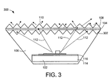
- FIG. 3 illustrates the white LED structure of the present invention with a roughened phosphor layer on both sides of the interface between the epoxy and the phosphor;
- FIG. 4 illustrates the one side roughened phosphor layer of the present invention placed directly on the LED chip
- FIG. 5 illustrates the dual-sided roughened phosphor layer of the present invention placed directly on the LED chip
- FIG. 6 illustrates the one side roughened phosphor layer of the present invention placed inside of the epoxy molding
- FIGS. 7 and 8 illustrate the dual-sided roughened phosphor layer of the present invention placed inside of the epoxy molding
- FIGS. 9 and 10 illustrate an LED structure of the present invention using thick epoxy layers
- FIG. 11 illustrates a cross-sectional view of an LED of the present invention molded into a spherical shape
- FIG. 12 illustrates the LED chip of the present invention with a roughened transparent oxide conductor layer
- FIG. 13 illustrates a current spreading layer in accordance with the present invention
- FIG. 14 illustrates a mirror placed outside of the spherical LED of the present invention
- FIG. 16 illustrates an internal mirror in accordance with the present invention
- FIG. 17 illustrates a emission schema in a direction normal to the LED emissions in accordance with the present invention
- FIG. 18 illustrates an alternative embodiment of the emission schema shown in FIG. 17 .
- FIG. 19 illustrates another embodiment of the present invention.
- FIG. 1 shows the structure of the white LEDs which utilize the phosphor to get the white emission color.
- the phosphor layer is located near the surface of the inverted cone shape epoxy molding.
- the surface of the phosphor layer is roughened, the luminous efficacy of the white LEDs is increased as shown in FIG. 2 in comparison with the white LEDs with a flat surface of the phosphor layer.
- the surface roughening improves the light extraction efficiency by reducing the reflection of the light at the interface between the phosphor layer and the air.
- the present invention also includes an (Al, Ga, In)N and light emitting diode (LED) in which the multiple directions of light can be extracted from the surfaces of the chip before then entering the shaped plastic optical element and subsequently extracted to air after exciting the phosphor.
- the (Al, Ga, In)N and transparent contact layers (ITO or ZnO) is combined with a shaped lens in which most light entering lens lies within the critical angle and is extracted.
- the present invention also includes a high efficient LED by minimizing the re-absorption of LED emission without any intentional mirrors attached to LED chip.
- the conventional LEDs have used a high reflective mirror in order to increase the front emission by reflecting the LED light forward direction. See FIGS. 1-3 .
- the present invention reduces reflection from the phosphor layer, plastic encapsulant surface, reflection from the ITO or ZnO surface, reduces reflection from the GaN by roughening, patterning or anisotropically etched surface (microcones), and minimizes light re-absorption by the emitting layer (active layer) without any intentional mirrors attached to LED chip, enables uniform light emitting from active layer to both sides of front and back sides.
- the present invention furthermore combines the high light extraction efficiency LED chip with shaped (textured) phosphor layers to increase the total luminous efficacy of the device. As a result, this combined structure extracts more light out of the LED. See FIGS. 4-19 .
- the details of the LED structure are not shown. Only the emitting layer (usually AlInGaN MQW), p-type GaN, n—GaN, sapphire substrate are shown. In the complete LED structure, there can be other layers such as p—AlGaN electron blocking layer, InGaN/GaN super lattices and others.
- the most important parts are surface of the LED chip because the light extraction efficiency is determined mainly by the surface layer or condition of the epitaxial wafers. So, only some parts (the surface layers) of the LED chip are shown in all of the figures.
- FIG. 1 illustrates a white LED structure of the present invention.
- Light Emitting Diode (LED) 100 comprises LED chip 102 and a phosphor layer 104 .
- the phosphor layer 104 is excited by the blue light from the LED chip 102 and converts the blue light, in the first wavelength region, to light in a second wavelength region.
- the phosphor layer is located near the surface of the inverted cone shape epoxy molding 106 to improve the conversion efficiency of the phosphor layer 104 .
- the surface 108 of the phosphor layer is roughened to increase the converted light extraction 110 from the phosphor layer 104 . At least a portion of surface 108 , rather than being completely planar, is roughened, textured, patterned, or otherwise made not normal to the light 112 emitted from the LED chip 102 so that reflection of light 112 is reduced. This irregular surface 108 may be generated through additional processing of phosphor layer 104 , or may occur as the phosphor layer 104 is applied to LED 100 , without departing from the scope of the present invention.
- LED chip 102 typically comprises a sapphire wafer 114 and a ITT-nitride LED active layer 116 .
- the active layer 116 typically emits blue light 112 , which excites phosphor layer 104 into producing yellow light 110 .
- a zinc oxide (ZnO) layer 106 can be formed with a refractive index that is between that of the LED chip 102 and that of air, and for ZnO layer 106 the refractive index n is 2.1.
- layer 106 can comprise ZnO, ITO, a thin metal, as well as an epoxy or some combination of these and other materials.
- layer 106 Any material can be used for layer 106 , so long as layer 106 is transmissive at the wavelengths being emitted by LED chip 102 .
- the blue light 112 and the yellow emissions 110 both emit from LED 100 to form white light that emits from the surface 118 of LED 100 .
- Graph 200 shows a chart of current on the x-axis and lumens per watt on the y-axis.
- Line 202 shows an un-roughened phosphor layer 104 , e.g., one with a flat upper surface rather than a roughened surface 108 .
- the surface 108 of the phosphor layer 104 is roughened, the luminous efficacy of the white LEDs is increased, as shown in graphs 204 and 206 , due to the improvement of the light extraction efficiency from the phosphor layer 104 .
- FIG. 3 illustrates the white LED structure with a roughened phosphor layer on both sides of the interface between the epoxy and the phosphor layer.
- the upper surface 108 is roughened or textured, and now, in LED 300 , at least a portion of the lower surface 302 of the phosphor layer 104 is also roughened or textured or otherwise made non-normal to the incident light 112 .
- This allows for less reflection of blue light 112 , and thus improves the efficiency of LED 300 , because now the light 112 that was previously reflected is now emitted from the upper surface 108 of LED 300 or excites phosphor layer 104 .
- the interface between the epoxy 106 and the phosphor layer 104 resulting in surface 302 , is roughened to improve the conversion efficiency of the phosphor layer 104 by reducing the reflection of the blue light 112 that is shown in FIG. 1 .
- the surface 302 can be created by texturing or roughening the surface of epoxy molding layer 106 , or by using other methods to generate a textured or roughened surface 302 . Further, the surface 302 may not be uniformly roughened or textured; the texture may take on different characteristics depending on where the LED chip 102 is located with respect to the surface 302 .
- FIG. 4 illustrates the one side roughened phosphor layer of the present invention placed directly on the LED chip.
- the phosphor layer 104 can be placed directly on LED chip 102 , and have a patterned, textured, or roughened upper surface 108 as described previously, such that LED 400 will also have an increased efficiency.
- the approach shown in LED 400 also reduces reflection of blue light 112 , and increases efficiency, because there is no reflecting surface between the emission of the LED chip 102 and the phosphor layer 104 .
- FIG. 5 illustrates the dual-sided roughened phosphor layer of the present invention placed directly on the LED chip.
- LED 402 shows that a dual-sided roughened phosphor layer 104 , i.e., with surfaces 108 and 302 , can also be placed directly on LED chip 102 , to increase efficiency further.
- FIG. 6 illustrates the one side roughened phosphor layer of the present invention placed inside of the epoxy molding.
- LED 404 uses a phosphor layer 104 inside of the epoxy layer 106 , rather than on top of epoxy layer 106 as shown in FIGS. 1 and 3 . This protects the phosphor layer 104 and upper surface 108 to allow for long-term high efficiency of LED 404 .
- FIGS. 7 and 8 illustrate the dual-sided roughened phosphor layer of the present invention placed inside of the epoxy molding.
- FIG. 7 shows LED 406 that has an internal phosphor layer 104 , with textured or roughened surfaces 108 and 302 .
- FIGS. 8A and 8B illustrate an embodiment of the LED of the present invention.
- LED 500 with emitted light 502 and active layer 504 are shown.
- Lead frame 506 and electrode 508 are shown as supporting glass plate 510 .
- the LED structure 500 is shown as being grown on a sapphire substrate.
- ITO Indium Tin Oxide
- layer 512 is deposited on p-type GaN layer 514 .
- an ITO layer 516 is coated onto glass plate 510 , and is attached to the deposited ITO layer 512 using epoxy as a glue.
- the other side 518 of glass plate 510 is roughened, patterned, or otherwise given a non-planar profile by a sand blast or other roughening technique, such as etching.
- the sapphire substrate is removed using the laser de-bonding technique.
- the Nitrogen-face (N face) GaN 520 is etched with wet etching such as KOH or HCL.
- LED chip 500 is put on a lead frame 506 which works for removing any heat that is generated by the LED chip 500 .
- the wire bonding 524 and 526 is done between bonding pads of the LED chip 528 and 530 and a lead frame 506 and electrode 508 to allow an electric current to flow through the lead frame 506 .
- the lead frame 506 is designed to extract the light from the back side of the LED chip effectively as shown in the figure, because lead frame 506 acts as a support around the edges of LED chip 500 , rather than supporting the entire underside of chip 500 .
- the LED light 532 is effectively extracted to both sides as emitted light 502 .
- the ohmic contact below the bonding pad of n—GaN is not shown for simplicity.
- the LED chip 500 is molded with a sphere shape molding 100 of plastic, epoxy, or glass, which acts as a lens to assist the emitted light 532 to escape from the LED and enter the air.
- FIG. 9 illustrates additional details of an embodiment of the present invention
- FIG. 10 illustrates details of another embodiment of the present invention.
- FIGS. 9 and 10 instead of the glass layer 510 as shown in FIG. 5 , a thick epoxy 600 is used. To make the electric contact, the epoxy 600 is partially removed, and ITO or a narrow stripe Au layer 602 is deposited on the epoxy 600 and the hole 604 . The operation of the LED is similar to the LED described with respect to FIG. 8 , except layer 514 is now roughened on the opposite side of active layer 504 to allow for additional light to be emitted from the reverse side of active layer 502 .
- the laser de-bonding step is not required, and, as such, the glass and thick epoxy sub-mount are also not required.
- ITO is deposited on p-type GaN and the backside of GaN substrate (typically Nitrogen-face GaN) is etched with a wet etching such as KOH and HCL. Then a cone-shaped surface is formed on the Nitrogen face GaN. The remainder of the fabrication and operational steps are similar to the LED described with respect to FIG. 8 .
- ITO layers e.g., layers 512 , 516 , etc.
- the roughening of the surface of p-type GaN 514 as surface 700 is effective to increase the light extraction through the p-type GaN 514 .
- ITO or ZnO are typically used after the surface roughening of Nitrogen-face GaN layer 520 . Since ITO and ZnO have a similar refractive index as GaN, the light reflection at the interface between ITO (ZnO) and GaN is minimized.
- FIGS. 11-14 illustrates embodiments of a spherical LED in accordance with the present invention.
- the LED chip of FIG. 5 is molded with epoxy or glass 800 as a sphere shape.
- the light 532 is extracted to air through the sphere molding 800 effectively, because the LED chip 500 is a small spot light source compared to the diameter of the spherical lens 800 .
- a phosphor layer 802 is placed or deposited near the outside surface of the lens molding 800 . In this case, the conversion efficiency of the blue light to white light is increased due to a small re-absorption of the LED light 532 due to a small back scattering of the LED light 532 by the phosphor layer 802 .
- FIG. 11B illustrates that chip 500 is mounted on frame 506 such that light 532 is also emitted from led 500 via surface 518 on the back side of chip 500 .
- the ITO or ZnO is roughened as surface 700 to improve the light extraction through the ITO or ZnO. Then, the epoxy 900 is sub-mounted.
- a current spreading layer (SiO2, SiN, transparent insulating material) 1000 is deposited to allow a uniform current to flow through the p-type GaN layer 512 , and contact 1002 is provided to contact frame 506 .
- a mirror 1100 is put outside of the sphere molding 800 in order to direct more light to a specific side of the LED package 500 .
- the shape of the mirror 1100 is typically designed such that any reflected light is directed away from the LED chip 500 to avoid or minimize reabsorption of light by the active layer 502 of the LED chip 500 .
- FIG. 15 illustrates another embodiment of the present invention.
- LED 1500 comprises an LED structure 1502 with an emitting layer 1504 that is grown on a flat sapphire substrate or a patterned sapphire substrate (PSS) 1506 to improve the light extraction efficiency through the interface between the LED structure 1502 and the sapphire substrate 1506 .
- the backside of the sapphire substrate 1506 is roughened to increase the light extraction from the sapphire substrate 1506 to the air or epoxy or glass 1508 .
- a preferred shape of the roughened surface is typically a cone-shaped surface, but other surface topologies can be used without departing from the scope of the present invention.
- an ITO or ZnO layer 1510 was deposited on p-type GaN. Then, bonding pad 1512 was formed on the ITO or ZnO layer 1510 , and an Ohmic contact/bonding pad 1514 on n-type GaN layer 1516 are formed after disclosing the n-type GaN by a selective etching through p-type GaN. Wire bonds 1518 and 1520 are added to connect the LED structure 1502 to the lead frame 1522 .
- the LED chip 1502 was molded as an inverted cone-shape for both the front and back sides by shaping epoxy/glass layers 1508 into inverted cone shapes.
- the phosphor layers 1524 were put near the top surface of the glass/epoxy layers 1508 molding. Typically, this means that the phosphor layer is placed at a distance far away from the LED chip 1502 . In this case, the conversion efficiency of the blue light to white light is increased due to a small re-absorption of the LED light due to a small back scattering by the phosphor to the LED chip.
- the surfaces 1526 and 1528 of the phosphor layers 1524 are roughened to improve the light extraction through the phosphor.
- the surfaces 1526 and 1528 may have different patterns or may be roughened in the same fashion as each other, as desired.
- FIG. 16 illustrates an internal mirror in accordance with the present invention.
- a mirror 1600 was put inside of the molding of epoxy/glass layer 1508 shown in FIG. 15 to increase the light output to a front side 1602 of LED chip 1502 .
- the shape of the mirror 1600 was designed for the reflected light not to reach the LED chip 1502 . If the reflected light can reach the LED chip 1502 , the LED light 1604 would be re-absorbed by the LED chip 1502 , which decreases the output power or the efficiency of the LED chip 1502 , and thus the efficiency of the LED 1600 would also drop.
- the mirror 1600 is partially attached to the LED chip 1502 or the substrate 1506 .
- This partial attachment of the mirror 1600 is not defined as attached mirror to the LED chip 1502 because the mirror of a conventional LED chip is attached to the whole rear surface of the LED chip at the front or the back sides of the LED chip, which would allow for re-absorption of the light within the LED chip, which is undesirable.
- the phosphor layer 1524 was put near the top surface of the molding layer 1508 . Again, this means that the phosphor layer 1524 should be put far away from the LED chip 1502 to allow the light to escape the LED chip 1502 . In this case, the conversion efficiency of the blue light to white light is increased due to a small re-absorption of the LED light due to a small back scattering by the phosphor layer 1524 . Then surface 1528 of the phosphor layer 1524 was roughened to improve the light extraction through the phosphor layer 1524 .
- FIGS. 17A and B illustrate an emission schema in a direction normal to the LED emissions in accordance with the present invention.
- LED 1700 comprises mirrors 1702 and 1704 and molding 1508 are designed as shown.
- the LED light 1604 is obtained from the direction of the side wall, or normal to the top emitting surface of the LED chip 1502 .
- the phosphor layer 1524 was put near the top surface of the molding 1508 .
- the conversion efficiency of the blue light to white light is increased due to a small re-absorption of the LED light 1604 due to a small back scattering by the phosphor layer 1524 to the LED chip.
- the surface 1528 of the phosphor layer 1524 is roughened to improve the conversion efficiency of the phosphor layer 1524 from blue light to yellow light.
- 17B shows lead frame 1522 with electrodes 1706 and 1708 , which allow light to pass through electrode 1706 through substrate 1506 and contribute to the light emitting from LED 1700 , increasing the efficiency of LED 1700 .
- these mirrors 1702 and 1704 can be a single mirror 1702 that is shaped as a conical or parabolic reflector to maximize the light emitting through surface 1528 if desired.
- FIGS. 18A and 18B illustrate an alternative embodiment of the emission schema shown in FIG. 17 .
- LED 1800 has mirrors 1702 and 1704 inside of the molding 1508 removed.
- the shape of the molding 1508 is an inverted cone shape.
- the angle 1802 of the inverted cone is determined for all of the LED light 1604 to reflect to the front side 1804 of LED 1800 .
- the critical angle of the reflection is sin ⁇ 1 (1/1.5). So, the angle of the inverted cone 1802 should be more than sin ⁇ 1 (1/1.5). Then the LED light 1604 is effectively extracted from the front surface 1804 of the inverted cone, which is approximately parallel to the side wall of the LED chip 1502 .
- a mirror 1806 coating can be applied to the epoxy layer 1508 to increase the reflection of the rear surface of the epoxy layer 1508 if desired.
- the phosphor layer 1524 is put near the top surface of the inverted cone-shape molding 1508 , which places the phosphor layer 1524 relatively far away from the LED chip 1502 .
- the conversion efficiency of the blue light to white light is increased due to a small re-absorption of the LED light 1604 due to a small back scattering by the phosphor layer 1524 to the LED chip 1502 .
- surface 1528 of the phosphor layer 1524 is roughened to improve the conversion efficiency of the phosphor layer 1524 from blue to yellow emission.
- the details of lead frame 1522 are shown in FIG. 17B .
- FIGS. 19A and B illustrates another embodiment of the present invention.
- LED 1900 uses a lead frame 1522 where the LED chip 1502 is placed that also uses a transparent plate 1902 such as glass, quartz and other materials, which is attached to the lead frame using a transparent epoxy 1904 as a die-bonding material.
- the transparent glass plate is used to extract the LED light 1604 to the epoxy molding 1508 on the underside of LED 1900 effectively.
- the details of lead frame 1522 are shown in FIG. 19B .
- Other portions of LED 1900 are similar to those described with respect to FIGS. 16-18 .
- the conversion efficiency of the phosphor layer is increased by increasing the light extraction from the phosphor layer and also by increasing the excitation efficiency of the phosphor layer.
- the mirror coated on lead frame is also included as the intentional mirrors
- the re-absorption of LED light is minimized and the light extraction efficiency is increased dramatically. Then, the light output power of the LEDs is increased dramatically. See FIGS. 4-19 .
- a Light Emitting Diode in accordance with the present invention comprises an LED chip, emitting light at a first wavelength region, an encapsulation layer, coupled to the LED chip, wherein the encapsulation layer is transparent at the first wavelength region, and a phosphor layer, coupled to the encapsulation layer and distant from the LED chip, the phosphor layer converting the light emitted by the LED chip in the first wavelength region to light in at least a second wavelength region, wherein at least a portion of a surface of the phosphor layer is textured.
- LED Light Emitting Diode
- Such an LED further optionally comprises the LED being made from a material selected from the group comprising (Al, Ga, In)N material system, the (Al, Ga, In)As material system, the (Al, Ga, In)P material system, the (Al, Ga, In) AsPNSb material system, and the ZnGeN2 and ZnSnGeN2 material systems, the textured phosphor layer having a cone shape, the encapsulation layer comprising epoxy, glass, air, and other materials that are transparent at the emission wavelength, at least a portion of a second surface of the phosphor layer being textured, the encapsulation layer comprising a material selected from a group comprising ITO, ZnO, and a thin metal, the LED chip further comprising a current spreading layer, a textured sapphire substrate being used for the LED chip to increase the light transmission from the LED chip, a backside of the textured sapphire substrate being textured, the LED being molded into an inverted cone shape, light being extracted from the
- Another LED in accordance with the present invention comprises an LED chip, emitting light at a first wavelength region and having a first refractive index, an encapsulation layer, coupled to the LED chip, wherein the encapsulation layer is transparent at the first wavelength region and having a second refractive index less than the first refractive index, wherein the second refractive index is greater than 1, and a phosphor layer, coupled to the encapsulation layer and distant from the LED chip, the phosphor layer converting light emitted in the first wavelength region to light in at least a second wavelength region, wherein at least a portion of a surface of the phosphor layer farthest from the LED chip is not normal to the light emitted from the LED chip.
- Such an LED further optionally comprises the LED being made from a material selected from the group comprising (Al, Ga, In)N material system, the (Al, Ga, In)As material system, the (Al, Ga, In)P material system, the (Al, Ga, In) AsPNSb material system, and the ZnGeN2 and ZnSnGeN2 material systems, the phosphor layer having a cone shape, at least a portion of a second surface of the phosphor layer closer to the LED chip also being textured, the encapsulation layer comprising a material selected from a group comprising ITO, ZnO, and a thin metal, the LED chip further comprising a current spreading layer, and the encapsulation layer comprising epoxy, glass, and other materials that are transparent at the emission wavelength.
- the LED being made from a material selected from the group comprising (Al, Ga, In)N material system, the (Al, Ga, In)As material system, the (Al, Ga, In)P material system
Priority Applications (4)
| Application Number | Priority Date | Filing Date | Title |
|---|---|---|---|
| US11/940,885 US8860051B2 (en) | 2006-11-15 | 2007-11-15 | Textured phosphor conversion layer light emitting diode |
| US14/461,151 US10217916B2 (en) | 2004-06-03 | 2014-08-15 | Transparent light emitting diodes |
| US14/483,501 US9240529B2 (en) | 2004-07-06 | 2014-09-11 | Textured phosphor conversion layer light emitting diode |
| US14/757,937 US9859464B2 (en) | 2004-07-06 | 2015-12-23 | Lighting emitting diode with light extracted from front and back sides of a lead frame |
Applications Claiming Priority (2)
| Application Number | Priority Date | Filing Date | Title |
|---|---|---|---|
| US86602406P | 2006-11-15 | 2006-11-15 | |
| US11/940,885 US8860051B2 (en) | 2006-11-15 | 2007-11-15 | Textured phosphor conversion layer light emitting diode |
Related Child Applications (1)
| Application Number | Title | Priority Date | Filing Date |
|---|---|---|---|
| US14/483,501 Continuation US9240529B2 (en) | 2004-07-06 | 2014-09-11 | Textured phosphor conversion layer light emitting diode |
Publications (2)
| Publication Number | Publication Date |
|---|---|
| US20080128730A1 US20080128730A1 (en) | 2008-06-05 |
| US8860051B2 true US8860051B2 (en) | 2014-10-14 |
Family
ID=39402256
Family Applications (3)
| Application Number | Title | Priority Date | Filing Date |
|---|---|---|---|
| US11/940,885 Active 2028-11-04 US8860051B2 (en) | 2004-06-03 | 2007-11-15 | Textured phosphor conversion layer light emitting diode |
| US14/483,501 Active US9240529B2 (en) | 2004-07-06 | 2014-09-11 | Textured phosphor conversion layer light emitting diode |
| US14/757,937 Active US9859464B2 (en) | 2004-07-06 | 2015-12-23 | Lighting emitting diode with light extracted from front and back sides of a lead frame |
Family Applications After (2)
| Application Number | Title | Priority Date | Filing Date |
|---|---|---|---|
| US14/483,501 Active US9240529B2 (en) | 2004-07-06 | 2014-09-11 | Textured phosphor conversion layer light emitting diode |
| US14/757,937 Active US9859464B2 (en) | 2004-07-06 | 2015-12-23 | Lighting emitting diode with light extracted from front and back sides of a lead frame |
Country Status (4)
| Country | Link |
|---|---|
| US (3) | US8860051B2 (ja) |
| EP (2) | EP2087563B1 (ja) |
| JP (2) | JP2010510659A (ja) |
| WO (1) | WO2008060586A2 (ja) |
Cited By (48)
| Publication number | Priority date | Publication date | Assignee | Title |
|---|---|---|---|---|
| US20150084081A1 (en) * | 2012-02-16 | 2015-03-26 | Korea University Research And Business Foundation | Method for manufacturing light-emitting device and light-emitting device manufactured using same |
| US20150371974A1 (en) * | 2014-06-18 | 2015-12-24 | X-Celeprint Limited | Micro assembled led displays and lighting elements |
| US20160133790A1 (en) * | 2004-07-06 | 2016-05-12 | The Regents Of The University Of California | Textured phosphor conversion layer light emitting diode |
| US9716082B2 (en) | 2014-08-26 | 2017-07-25 | X-Celeprint Limited | Micro assembled hybrid displays and lighting elements |
| US9741785B2 (en) | 2014-09-25 | 2017-08-22 | X-Celeprint Limited | Display tile structure and tiled display |
| US9786646B2 (en) | 2015-12-23 | 2017-10-10 | X-Celeprint Limited | Matrix addressed device repair |
| US9818725B2 (en) | 2015-06-01 | 2017-11-14 | X-Celeprint Limited | Inorganic-light-emitter display with integrated black matrix |
| US9871345B2 (en) | 2015-06-09 | 2018-01-16 | X-Celeprint Limited | Crystalline color-conversion device |
| US9980341B2 (en) | 2016-09-22 | 2018-05-22 | X-Celeprint Limited | Multi-LED components |
| US9991163B2 (en) | 2014-09-25 | 2018-06-05 | X-Celeprint Limited | Small-aperture-ratio display with electrical component |
| US9997100B2 (en) | 2014-09-25 | 2018-06-12 | X-Celeprint Limited | Self-compensating circuit for faulty display pixels |
| US9997102B2 (en) | 2016-04-19 | 2018-06-12 | X-Celeprint Limited | Wirelessly powered display and system |
| US9997501B2 (en) | 2016-06-01 | 2018-06-12 | X-Celeprint Limited | Micro-transfer-printed light-emitting diode device |
| US10008465B2 (en) | 2011-06-08 | 2018-06-26 | X-Celeprint Limited | Methods for surface attachment of flipped active components |
| US10008483B2 (en) | 2016-04-05 | 2018-06-26 | X-Celeprint Limited | Micro-transfer printed LED and color filter structure |
| US20180182934A1 (en) * | 2016-12-22 | 2018-06-28 | Osram Opto Semiconductors Gmbh | Light Emitting Unit |
| US10066819B2 (en) | 2015-12-09 | 2018-09-04 | X-Celeprint Limited | Micro-light-emitting diode backlight system |
| US10109753B2 (en) | 2016-02-19 | 2018-10-23 | X-Celeprint Limited | Compound micro-transfer-printed optical filter device |
| US10133426B2 (en) | 2015-06-18 | 2018-11-20 | X-Celeprint Limited | Display with micro-LED front light |
| US10153257B2 (en) | 2016-03-03 | 2018-12-11 | X-Celeprint Limited | Micro-printed display |
| US10150325B2 (en) | 2016-02-29 | 2018-12-11 | X-Celeprint Limited | Hybrid banknote with electronic indicia |
| US10150326B2 (en) | 2016-02-29 | 2018-12-11 | X-Celeprint Limited | Hybrid document with variable state |
| US10153256B2 (en) | 2016-03-03 | 2018-12-11 | X-Celeprint Limited | Micro-transfer printable electronic component |
| US10193025B2 (en) | 2016-02-29 | 2019-01-29 | X-Celeprint Limited | Inorganic LED pixel structure |
| US10200013B2 (en) | 2016-02-18 | 2019-02-05 | X-Celeprint Limited | Micro-transfer-printed acoustic wave filter device |
| US10198890B2 (en) | 2016-04-19 | 2019-02-05 | X-Celeprint Limited | Hybrid banknote with electronic indicia using near-field-communications |
| US10199546B2 (en) | 2016-04-05 | 2019-02-05 | X-Celeprint Limited | Color-filter device |
| US10217730B2 (en) | 2016-02-25 | 2019-02-26 | X-Celeprint Limited | Efficiently micro-transfer printing micro-scale devices onto large-format substrates |
| US10224231B2 (en) | 2016-11-15 | 2019-03-05 | X-Celeprint Limited | Micro-transfer-printable flip-chip structures and methods |
| US10230048B2 (en) | 2015-09-29 | 2019-03-12 | X-Celeprint Limited | OLEDs for micro transfer printing |
| US10255834B2 (en) | 2015-07-23 | 2019-04-09 | X-Celeprint Limited | Parallel redundant chiplet system for controlling display pixels |
| US10347168B2 (en) | 2016-11-10 | 2019-07-09 | X-Celeprint Limited | Spatially dithered high-resolution |
| US10361677B2 (en) | 2016-02-18 | 2019-07-23 | X-Celeprint Limited | Transverse bulk acoustic wave filter |
| US10380930B2 (en) | 2015-08-24 | 2019-08-13 | X-Celeprint Limited | Heterogeneous light emitter display system |
| US10395966B2 (en) | 2016-11-15 | 2019-08-27 | X-Celeprint Limited | Micro-transfer-printable flip-chip structures and methods |
| US10396137B2 (en) | 2017-03-10 | 2019-08-27 | X-Celeprint Limited | Testing transfer-print micro-devices on wafer |
| US10418331B2 (en) | 2010-11-23 | 2019-09-17 | X-Celeprint Limited | Interconnection structures and methods for transfer-printed integrated circuit elements with improved interconnection alignment tolerance |
| US10438859B2 (en) | 2016-12-19 | 2019-10-08 | X-Celeprint Limited | Transfer printed device repair |
| US10454010B1 (en) | 2006-12-11 | 2019-10-22 | The Regents Of The University Of California | Transparent light emitting diodes |
| US10600671B2 (en) | 2016-11-15 | 2020-03-24 | X-Celeprint Limited | Micro-transfer-printable flip-chip structures and methods |
| US10782002B2 (en) | 2016-10-28 | 2020-09-22 | X Display Company Technology Limited | LED optical components |
| US10836200B2 (en) * | 2017-11-13 | 2020-11-17 | X Display Company Technology Limited | Rigid micro-modules with ILED and light conductor |
| US11024608B2 (en) | 2017-03-28 | 2021-06-01 | X Display Company Technology Limited | Structures and methods for electrical connection of micro-devices and substrates |
| US11061276B2 (en) | 2015-06-18 | 2021-07-13 | X Display Company Technology Limited | Laser array display |
| US11137641B2 (en) | 2016-06-10 | 2021-10-05 | X Display Company Technology Limited | LED structure with polarized light emission |
| US11177460B2 (en) * | 2017-05-12 | 2021-11-16 | Boe Technology Group Co., Ltd. | Sub-pixel structure, pixel structure, display panel and display device |
| US11592166B2 (en) | 2020-05-12 | 2023-02-28 | Feit Electric Company, Inc. | Light emitting device having improved illumination and manufacturing flexibility |
| US11876042B2 (en) | 2020-08-03 | 2024-01-16 | Feit Electric Company, Inc. | Omnidirectional flexible light emitting device |
Families Citing this family (76)
| Publication number | Priority date | Publication date | Assignee | Title |
|---|---|---|---|---|
| US7781789B2 (en) * | 2006-11-15 | 2010-08-24 | The Regents Of The University Of California | Transparent mirrorless light emitting diode |
| US9130119B2 (en) * | 2006-12-11 | 2015-09-08 | The Regents Of The University Of California | Non-polar and semi-polar light emitting devices |
| US10655792B2 (en) * | 2014-09-28 | 2020-05-19 | Zhejiang Super Lighting Electric Appliance Co., Ltd. | LED bulb lamp |
| JP5372766B2 (ja) * | 2006-11-15 | 2013-12-18 | ザ リージェンツ オブ ザ ユニバーシティ オブ カリフォルニア | 光取り出し効率の高い球形led |
| US20090121250A1 (en) * | 2006-11-15 | 2009-05-14 | Denbaars Steven P | High light extraction efficiency light emitting diode (led) using glass packaging |
| TWI533351B (zh) | 2006-12-11 | 2016-05-11 | 美國加利福尼亞大學董事會 | 高效能非極性第三族氮化物光學裝置之金屬有機化學氣相沈積生長 |
| EP2174351A1 (en) | 2007-07-26 | 2010-04-14 | The Regents of the University of California | Light emitting diodes with a p-type surface |
| KR101383357B1 (ko) * | 2007-08-27 | 2014-04-10 | 엘지이노텍 주식회사 | 발광 소자 패키지 및 그 제조방법 |
| DE102007046849B4 (de) * | 2007-09-29 | 2014-11-06 | Advanced Micro Devices, Inc. | Verfahren zur Herstellung von Gateelektrodenstrukturen mit großem ε nach der Transistorherstellung |
| US7897985B2 (en) * | 2008-03-14 | 2011-03-01 | Osram Sylvania | LED light engine kernel and method of making the kernel |
| WO2009119034A1 (en) | 2008-03-26 | 2009-10-01 | Panasonic Corporation | Semiconductor light-emitting apparatus |
| US8105853B2 (en) * | 2008-06-27 | 2012-01-31 | Bridgelux, Inc. | Surface-textured encapsulations for use with light emitting diodes |
| TWI384651B (zh) * | 2008-08-20 | 2013-02-01 | Au Optronics Corp | 發光二極體結構及其製造方法 |
| JP2010062493A (ja) * | 2008-09-08 | 2010-03-18 | Stanley Electric Co Ltd | 半導体発光素子および半導体発光素子の製造方法 |
| US7825427B2 (en) * | 2008-09-12 | 2010-11-02 | Bridgelux, Inc. | Method and apparatus for generating phosphor film with textured surface |
| JP5431706B2 (ja) * | 2008-10-01 | 2014-03-05 | ミネベア株式会社 | 発光装置 |
| US8329060B2 (en) | 2008-10-22 | 2012-12-11 | General Electric Company | Blue-green and green phosphors for lighting applications |
| US8703016B2 (en) | 2008-10-22 | 2014-04-22 | General Electric Company | Phosphor materials and related devices |
| WO2010096578A1 (en) * | 2009-02-18 | 2010-08-26 | Osram Sylvania Inc. | Light source with leds, light guide and reflector |
| US20120098017A1 (en) * | 2009-05-15 | 2012-04-26 | Koito Manufacturing Co., Ltd. | Light emitting module, method of producing light-emitting module, and lighting fixture unit |
| DE102009023351A1 (de) | 2009-05-29 | 2010-12-02 | Osram Opto Semiconductors Gmbh | Optoelektronischer Halbleiterchip und Verfahren zur Herstellung eines optoelektronischen Halbleiterchips |
| JP5555318B2 (ja) | 2009-06-04 | 2014-07-23 | コーニンクレッカ フィリップス エヌ ヴェ | 効率の高い発光デバイス及び斯様なデバイスを製造する方法 |
| EP2443673B1 (de) * | 2009-06-19 | 2019-10-02 | OSRAM GmbH | Konversions-led mit erhöhter stabilität und verfahren zu ihrer herstellung |
| TWI396310B (zh) * | 2009-10-02 | 2013-05-11 | Everlight Electronics Co Ltd | 發光二極體結構 |
| US8783915B2 (en) | 2010-02-11 | 2014-07-22 | Bridgelux, Inc. | Surface-textured encapsulations for use with light emitting diodes |
| US8384105B2 (en) | 2010-03-19 | 2013-02-26 | Micron Technology, Inc. | Light emitting diodes with enhanced thermal sinking and associated methods of operation |
| JP5497520B2 (ja) * | 2010-04-14 | 2014-05-21 | 株式会社小糸製作所 | 発光モジュールおよび光波長変換部材 |
| JP5331051B2 (ja) * | 2010-04-21 | 2013-10-30 | パナソニック株式会社 | 発光素子 |
| KR101735670B1 (ko) * | 2010-07-13 | 2017-05-15 | 엘지이노텍 주식회사 | 발광 소자 |
| WO2012039168A1 (ja) * | 2010-09-21 | 2012-03-29 | 日本電気株式会社 | 蛍光体発光装置 |
| DE102010049312B4 (de) | 2010-10-22 | 2023-08-03 | OSRAM Opto Semiconductors Gesellschaft mit beschränkter Haftung | Verfahren zur Herstellung eines Konversionsplättchens und Konversionsplättchen |
| EP2450625B1 (en) * | 2010-11-08 | 2016-08-17 | LG Innotek Co., Ltd. | Lighting device comprising photoluminescent plate |
| US8314566B2 (en) | 2011-02-22 | 2012-11-20 | Quarkstar Llc | Solid state lamp using light emitting strips |
| TW201306323A (zh) | 2011-07-31 | 2013-02-01 | Walsin Lihwa Corp | 發光二極體裝置 |
| CN102916004A (zh) * | 2011-07-31 | 2013-02-06 | 华新丽华股份有限公司 | 发光二极管装置 |
| DE102011114641B4 (de) * | 2011-09-30 | 2021-08-12 | OSRAM Opto Semiconductors Gesellschaft mit beschränkter Haftung | Optoelektronisches Halbleiterbauelement und Verfahren zur Herstellung eines optoelektronischen Halbleiterbauelements |
| KR101969334B1 (ko) * | 2011-11-16 | 2019-04-17 | 엘지이노텍 주식회사 | 발광 소자 및 이를 구비한 발광 장치 |
| TW201327926A (zh) * | 2011-12-30 | 2013-07-01 | Ind Tech Res Inst | 光轉換結構和其應用之發光二極體的封裝結構 |
| WO2013121051A1 (en) * | 2012-02-16 | 2013-08-22 | University College Cork, National University Of Ireland, Cork | Micro -led array with filters |
| US10096742B2 (en) | 2012-03-28 | 2018-10-09 | Sensor Electronic Technology, Inc. | Light emitting device substrate with inclined sidewalls |
| US9595636B2 (en) | 2012-03-28 | 2017-03-14 | Sensor Electronic Technology, Inc. | Light emitting device substrate with inclined sidewalls |
| KR101364170B1 (ko) * | 2012-06-05 | 2014-02-20 | 포항공과대학교 산학협력단 | 백색 발광 다이오드 |
| TW201347238A (zh) | 2012-07-11 | 2013-11-16 | Walsin Lihwa Corp | 發光二極體裝置 |
| DE102012215113B4 (de) * | 2012-08-24 | 2022-02-03 | Pictiva Displays International Limited | Organische Leuchtdiode und Verfahren zum Betreiben einer organischen Leuchtdiode |
| JP2014082401A (ja) * | 2012-10-18 | 2014-05-08 | Ushio Inc | 蛍光光源装置 |
| US10125971B2 (en) * | 2013-02-19 | 2018-11-13 | Michael Graziano | LED lamp integrated to electric fan |
| JP2015015418A (ja) * | 2013-07-08 | 2015-01-22 | シャープ株式会社 | 半導体発光装置 |
| KR102076243B1 (ko) * | 2013-09-04 | 2020-02-12 | 엘지이노텍 주식회사 | 발광 소자 패키지 |
| KR20150039475A (ko) * | 2013-10-02 | 2015-04-10 | 엘지이노텍 주식회사 | 발광소자 |
| US11543083B2 (en) | 2014-09-28 | 2023-01-03 | Zhejiang Super Lighting Electric Appliance Co., Ltd | LED filament and LED light bulb |
| US11421827B2 (en) | 2015-06-19 | 2022-08-23 | Zhejiang Super Lighting Electric Appliance Co., Ltd | LED filament and LED light bulb |
| US11525547B2 (en) | 2014-09-28 | 2022-12-13 | Zhejiang Super Lighting Electric Appliance Co., Ltd | LED light bulb with curved filament |
| US11690148B2 (en) | 2014-09-28 | 2023-06-27 | Zhejiang Super Lighting Electric Appliance Co., Ltd. | LED filament and LED light bulb |
| US11686436B2 (en) | 2014-09-28 | 2023-06-27 | Zhejiang Super Lighting Electric Appliance Co., Ltd | LED filament and light bulb using LED filament |
| US11085591B2 (en) | 2014-09-28 | 2021-08-10 | Zhejiang Super Lighting Electric Appliance Co., Ltd | LED light bulb with curved filament |
| US11073248B2 (en) | 2014-09-28 | 2021-07-27 | Zhejiang Super Lighting Electric Appliance Co., Ltd. | LED bulb lamp |
| KR102315124B1 (ko) * | 2015-07-02 | 2021-10-20 | 쑤저우 레킨 세미컨덕터 컴퍼니 리미티드 | 발광소자 패키지 |
| TWI591864B (zh) * | 2015-08-26 | 2017-07-11 | 廣科精密股份有限公司 | 發光裝置及其製備方法 |
| DE102016101442A1 (de) * | 2016-01-27 | 2017-07-27 | Osram Opto Semiconductors Gmbh | Konversionselement und strahlungsemittierendes Halbleiterbauelement mit einem solchen Konversionselement |
| DE102016105988A1 (de) * | 2016-04-01 | 2017-10-05 | Osram Opto Semiconductors Gmbh | Konverter zur teilweisen Konversion einer Primärstrahlung und lichtemittierendes Bauelement |
| JP2017220478A (ja) * | 2016-06-03 | 2017-12-14 | 株式会社ディスコ | 発光ダイオードチップの製造方法及び発光ダイオードチップ |
| JP2017220479A (ja) * | 2016-06-03 | 2017-12-14 | 株式会社ディスコ | 発光ダイオードチップの製造方法 |
| JP2017224727A (ja) * | 2016-06-15 | 2017-12-21 | 株式会社ディスコ | 発光ダイオードチップの製造方法及び発光ダイオードチップ |
| JP2018010900A (ja) * | 2016-07-11 | 2018-01-18 | 株式会社ディスコ | 発光ダイオードチップの製造方法 |
| KR20180089117A (ko) | 2017-01-31 | 2018-08-08 | 삼성전자주식회사 | Led장치 및 이를 이용한 led램프 |
| DE102017002333A1 (de) * | 2017-03-13 | 2018-09-13 | Azur Space Solar Power Gmbh | Leuchtdiode |
| JP2018155968A (ja) * | 2017-03-17 | 2018-10-04 | 日亜化学工業株式会社 | 透光性部材の製造方法及び発光装置の製造方法 |
| JP2018170333A (ja) * | 2017-03-29 | 2018-11-01 | 株式会社東芝 | 半導体装置及びその製造方法 |
| JP2018186166A (ja) * | 2017-04-25 | 2018-11-22 | 株式会社ディスコ | 発光ダイオードチップの製造方法及び発光ダイオードチップ |
| KR102430500B1 (ko) | 2017-05-30 | 2022-08-08 | 삼성전자주식회사 | 반도체 발광소자 및 이를 이용한 led 모듈 |
| US10964852B2 (en) | 2018-04-24 | 2021-03-30 | Samsung Electronics Co., Ltd. | LED module and LED lamp including the same |
| WO2020146318A1 (en) | 2019-01-07 | 2020-07-16 | Glint Photonics, Inc. | Antireflective structures for light emitting diodes |
| KR20220001872A (ko) * | 2020-06-30 | 2022-01-06 | 엘지이노텍 주식회사 | 조명 장치 및 이를 포함하는 램프 |
| US11549680B2 (en) | 2020-07-08 | 2023-01-10 | Feit Electric Company, Inc. | Mirror with light emitting elements and stand |
| WO2023136880A1 (en) * | 2022-01-13 | 2023-07-20 | Ohio State Innovation Foundation | Photonic materials |
| DE102022104459A1 (de) * | 2022-02-24 | 2023-08-24 | Ams-Osram International Gmbh | Optoelektronische leuchtvorrichtung und verfahren |
Citations (121)
| Publication number | Priority date | Publication date | Assignee | Title |
|---|---|---|---|---|
| US3607463A (en) | 1968-08-02 | 1971-09-21 | Varian Associates | Method for growing tin-doped n-type epitaxial gallium arsenide from the liquid state |
| US3999280A (en) | 1973-06-25 | 1976-12-28 | Amp Incorporated | Narrow lead contact for automatic face down bonding of electronic chips |
| US4026692A (en) | 1975-12-15 | 1977-05-31 | Corning Glass Works | Press molding optical articles from acid hydrated glasses |
| US4497974A (en) | 1982-11-22 | 1985-02-05 | Exxon Research & Engineering Co. | Realization of a thin film solar cell with a detached reflector |
| US5416870A (en) | 1993-12-03 | 1995-05-16 | Motorola, Inc. | Optoelectronic interface device and method with reflective surface |
| JPH0927642A (ja) | 1995-07-13 | 1997-01-28 | Clarion Co Ltd | 照明装置 |
| US5696389A (en) | 1994-03-15 | 1997-12-09 | Kabushiki Kaisha Toshiba | Light-emitting semiconductor device |
| US5775792A (en) | 1995-06-29 | 1998-07-07 | Siemens Microelectronics, Inc. | Localized illumination using TIR technology |
| US5780867A (en) | 1996-03-07 | 1998-07-14 | Sandia Corporation | Broadband light-emitting diode |
| JPH10200165A (ja) | 1997-01-14 | 1998-07-31 | Sanken Electric Co Ltd | 半導体発光装置 |
| US5932048A (en) | 1995-04-06 | 1999-08-03 | Komatsu Electronic Metals Co., Ltd. | Method of fabricating direct-bonded semiconductor wafers |
| US6155699A (en) | 1999-03-15 | 2000-12-05 | Agilent Technologies, Inc. | Efficient phosphor-conversion led structure |
| EP1081771A2 (en) | 1999-09-03 | 2001-03-07 | Hewlett-Packard Company | Light emitting device |
| US20010033135A1 (en) | 2000-03-31 | 2001-10-25 | Duggal Anil Raj | Organic electroluminescent devices with enhanced light extraction |
| US6357889B1 (en) | 1999-12-01 | 2002-03-19 | General Electric Company | Color tunable light source |
| US6373188B1 (en) | 1998-12-22 | 2002-04-16 | Honeywell International Inc. | Efficient solid-state light emitting device with excited phosphors for producing a visible light output |
| US20020085601A1 (en) | 2000-12-29 | 2002-07-04 | Arima Optoelectronics Corporation | Light emitting diode with light conversion using scattering optical media |
| US6417019B1 (en) | 2001-04-04 | 2002-07-09 | Lumileds Lighting, U.S., Llc | Phosphor converted light emitting diode |
| US20020123204A1 (en) | 2001-03-01 | 2002-09-05 | Torvik John Tarje | Method of making a hybrid substrate having a thin silicon carbide membrane layer |
| US6452217B1 (en) | 2000-06-30 | 2002-09-17 | General Electric Company | High power LED lamp structure using phase change cooling enhancements for LED lighting products |
| US20020158578A1 (en) | 2001-03-14 | 2002-10-31 | Gelcore, Llc | LED devices |
| JP2003016808A (ja) | 2001-06-29 | 2003-01-17 | Matsushita Electric Ind Co Ltd | 照明装置 |
| US6515308B1 (en) | 2001-12-21 | 2003-02-04 | Xerox Corporation | Nitride-based VCSEL or light emitting diode with p-n tunnel junction current injection |
| US6547423B2 (en) | 2000-12-22 | 2003-04-15 | Koninklijke Phillips Electronics N.V. | LED collimation optics with improved performance and reduced size |
| US6548956B2 (en) | 1994-12-13 | 2003-04-15 | The Trustees Of Princeton University | Transparent contacts for organic devices |
| US6569544B1 (en) | 1997-07-31 | 2003-05-27 | Ecole Polytechnique Federale De Lausanne | Electroluminescent device |
| US6573537B1 (en) | 1999-12-22 | 2003-06-03 | Lumileds Lighting, U.S., Llc | Highly reflective ohmic contacts to III-nitride flip-chip LEDs |
| US6573530B1 (en) | 2001-02-09 | 2003-06-03 | Nortel Networks Limited | Multiple quantum well optoelectronic devices |
| US6607286B2 (en) | 2001-05-04 | 2003-08-19 | Lumileds Lighting, U.S., Llc | Lens and lens cap with sawtooth portion for light emitting diode |
| US20030215766A1 (en) | 2002-01-11 | 2003-11-20 | Ultradent Products, Inc. | Light emitting systems and kits that include a light emitting device and one or more removable lenses |
| US6674096B2 (en) | 2001-06-08 | 2004-01-06 | Gelcore Llc | Light-emitting diode (LED) package and packaging method for shaping the external light intensity distribution |
| US6686218B2 (en) | 2001-03-15 | 2004-02-03 | Opto Tech Corporation | Method for packaging a high efficiency electro-optics device |
| US20040046179A1 (en) | 2001-03-09 | 2004-03-11 | Johannes Baur | Radiation-emitting semiconductor component and method for producing the semiconductor component |
| US6717362B1 (en) | 2002-11-14 | 2004-04-06 | Agilent Technologies, Inc. | Light emitting diode with gradient index layering |
| US20040079408A1 (en) | 2002-10-23 | 2004-04-29 | The Boeing Company | Isoelectronic surfactant suppression of threading dislocations in metamorphic epitaxial layers |
| US6729746B2 (en) | 2000-03-14 | 2004-05-04 | Toyoda Gosei Co., Ltd. | Light source device |
| US20040089868A1 (en) | 2002-11-06 | 2004-05-13 | Schang-Jing Hon | Gallium nitride based compound semiconductor light-emitting device and manufacturing method therefor |
| US6746295B2 (en) | 1999-04-22 | 2004-06-08 | Osram-Opto Semiconductors Gmbh & Co. Ohg | Method of producing an LED light source with lens |
| US6784460B2 (en) | 2002-10-10 | 2004-08-31 | Agilent Technologies, Inc. | Chip shaping for flip-chip light emitting diode |
| US20040211970A1 (en) | 2003-04-24 | 2004-10-28 | Yoshiaki Hayashimoto | Semiconductor light emitting device with reflectors having cooling function |
| US20050032257A1 (en) | 2000-09-12 | 2005-02-10 | Camras Michael D. | Method of forming light emitting devices with improved light extraction efficiency |
| US20050029528A1 (en) | 2003-08-06 | 2005-02-10 | Rohm Co., Ltd. | Semiconductor light emitting device |
| US20050035354A1 (en) | 2003-08-14 | 2005-02-17 | Dicon Fiberoptics, Inc | Light emiting diodes with current spreading layer |
| US20050062830A1 (en) | 2003-09-22 | 2005-03-24 | Fuji Photo Film Co., Ltd. | Light irradiating unit and optical fixing unit |
| US20050077532A1 (en) | 2000-12-28 | 2005-04-14 | Toyoda Gosei Co., Ltd. | Light emitting device |
| US20050082562A1 (en) | 2003-10-15 | 2005-04-21 | Epistar Corporation | High efficiency nitride based light emitting device |
| US20050093008A1 (en) | 2003-10-31 | 2005-05-05 | Toyoda Gosei Co., Ltd. | Light emitting element and light emitting device |
| US20050111240A1 (en) | 2003-10-08 | 2005-05-26 | Seiko Epson Corporation | Light source unit and projector |
| EP1536487A1 (en) | 2002-05-28 | 2005-06-01 | Matsushita Electric Works, Ltd. | Light emitting element, light emitting device and surface emission illuminating device using it |
| US20050121688A1 (en) | 2003-12-03 | 2005-06-09 | Sumitomo Electric Industries, Ltd. | Light emitting device |
| US20050133810A1 (en) | 1999-03-15 | 2005-06-23 | Roberts John K. | Opto-electronic assembly having an encapsulant with at least two different functional zones |
| JP2005191197A (ja) | 2003-12-25 | 2005-07-14 | Kyocera Corp | 発光装置 |
| WO2005064666A1 (en) | 2003-12-09 | 2005-07-14 | The Regents Of The University Of California | Highly efficient gallium nitride based light emitting diodes via surface roughening |
| US20050156510A1 (en) | 2004-01-21 | 2005-07-21 | Chua Janet B.Y. | Device and method for emitting output light using group IIB element selenide-based and group IIA element gallium sulfide-based phosphor materials |
| US20050184300A1 (en) | 2004-02-25 | 2005-08-25 | Mikio Tazima | Light-emitting semiconductor device and method of fabrication |
| US20050189551A1 (en) | 2004-02-26 | 2005-09-01 | Hui Peng | High power and high brightness white LED assemblies and method for mass production of the same |
| WO2005083037A1 (en) | 2004-02-20 | 2005-09-09 | Philips Intellectual Property & Standards Gmbh | Illumination system comprising a radiation source and a fluorescent material |
| US20050205884A1 (en) | 2004-03-19 | 2005-09-22 | Lumileds Lighting U.S., Llc | Semiconductor light emitting devices including in-plane light emitting layers |
| US20050212002A1 (en) | 2004-03-29 | 2005-09-29 | Daisuke Sanga | Semiconductor light emitting device |
| JP2005268323A (ja) | 2004-03-16 | 2005-09-29 | Sumitomo Electric Ind Ltd | 半導体発光装置 |
| US20050224830A1 (en) | 2004-04-09 | 2005-10-13 | Blonder Greg E | Illumination devices comprising white light emitting diodes and diode arrays and method and apparatus for making them |
| US6961190B1 (en) | 1999-07-26 | 2005-11-01 | Labosphere Institute | Bulk lens, light emitting body, lighting device and optical information system |
| US20050243570A1 (en) | 2004-04-23 | 2005-11-03 | Chaves Julio C | Optical manifold for light-emitting diodes |
| US20050248271A1 (en) * | 2004-05-07 | 2005-11-10 | Ng Kee Y | Method of applying light-converting material and device thereof |
| US20050265404A1 (en) * | 2004-05-28 | 2005-12-01 | Ian Ashdown | Luminance enhancement apparatus and method |
| US20060001186A1 (en) | 2004-06-30 | 2006-01-05 | Richardson Gary A | IOL and method of manufacturing an IOL |
| US20060009006A1 (en) | 2004-07-06 | 2006-01-12 | The Regents Of The University Of California | Method for wafer bonding (Al, In, Ga)N and Zn(S, Se) for optoelectronic applications |
| US20060008941A1 (en) | 2002-12-16 | 2006-01-12 | Basf Aktiengesellschaft | Growth of planar, non-polar a-plane gallium nitride by hydride vapor phase epitaxy |
| JP2006024615A (ja) | 2004-07-06 | 2006-01-26 | Matsushita Electric Ind Co Ltd | Led照明光源およびその製造方法 |
| JP2006032387A (ja) | 2004-07-12 | 2006-02-02 | Asahi Rubber:Kk | Ledランプ |
| US6997580B2 (en) | 2003-09-19 | 2006-02-14 | Mattel, Inc. | Multidirectional light emitting diode unit |
| US6998281B2 (en) | 2000-10-12 | 2006-02-14 | General Electric Company | Solid state lighting device with reduced form factor including LED with directional emission and package with microoptics |
| US20060054905A1 (en) | 2004-09-10 | 2006-03-16 | The Regents Of The University Of California | White, single or multi-color light emitting diodes by recycling guided modes |
| US7053419B1 (en) | 2000-09-12 | 2006-05-30 | Lumileds Lighting U.S., Llc | Light emitting diodes with improved light extraction efficiency |
| US20060138439A1 (en) | 2000-04-19 | 2006-06-29 | Georg Bogner | High radiance LED chip and a method for producing same |
| US20060145170A1 (en) | 2005-01-03 | 2006-07-06 | Samsung Electro-Mechanics Co., Ltd. | Nitride based semiconductor light emitting device |
| US20060163601A1 (en) | 2003-02-28 | 2006-07-27 | Volker Harle | Lighting module and method the production thereof |
| US20060171152A1 (en) * | 2005-01-20 | 2006-08-03 | Toyoda Gosei Co., Ltd. | Light emitting device and method of making the same |
| US20060175624A1 (en) | 2005-02-09 | 2006-08-10 | The Regents Of The University Of California | Semiconductor light-emitting device |
| US20060186418A1 (en) | 2004-05-18 | 2006-08-24 | Edmond John A | External extraction light emitting diode based upon crystallographic faceted surfaces |
| US7098589B2 (en) | 2003-04-15 | 2006-08-29 | Luminus Devices, Inc. | Light emitting devices with high light collimation |
| US20060194359A1 (en) | 2005-02-28 | 2006-08-31 | The Regents Of The University Of California | Horizontal emitting, vertical emitting, beam shaped, distributed feedback (DFB) lasers by growth over a patterned substrate |
| US20060192217A1 (en) | 2005-02-28 | 2006-08-31 | The Regents Of The University Of California | High efficiency light emitting diode (LED) with optimized photonic crystal extractor |
| JP2006237264A (ja) | 2005-02-24 | 2006-09-07 | Kyocera Corp | 発光装置および照明装置 |
| US20060202219A1 (en) | 2005-03-09 | 2006-09-14 | Kabushiki Kaisha Toshiba | Semiconductor light emitting device and semiconductor light emitting apparatus |
| US20060202226A1 (en) | 2005-02-28 | 2006-09-14 | The Regents Of The University Of California | Single or multi-color high efficiency light emitting diode (LED) by growth over a patterned substrate |
| US7119271B2 (en) | 2001-10-12 | 2006-10-10 | The Boeing Company | Wide-bandgap, lattice-mismatched window layer for a solar conversion device |
| US20060234486A1 (en) | 2005-04-13 | 2006-10-19 | Speck James S | Wafer separation technique for the fabrication of free-standing (Al,In,Ga)N wafers |
| US7126159B2 (en) | 2002-03-05 | 2006-10-24 | Rohm Co., Ltd. | Plural leds mounted within a central cutout of a surrounding circular reflective electrode |
| US20060237723A1 (en) | 2005-04-22 | 2006-10-26 | Kabushiki Kaisha Toshiba | Semiconductor device and method of manufacturing the same |
| US20060246722A1 (en) | 2005-04-13 | 2006-11-02 | Speck James S | Etching technique for the fabrication of thin (AI, In, Ga)N layers |
| JP2005191514A5 (ja) | 2004-04-01 | 2006-11-02 | ||
| US20060243993A1 (en) | 2005-04-29 | 2006-11-02 | Hon Hai Precision Industry Co., Ltd. | Light emitting diode chip and light emitting diode using the same |
| US7135709B1 (en) | 1999-09-30 | 2006-11-14 | Osram Gmbh | Surface structured light-emitting diode with improved current coupling |
| US20070001185A1 (en) | 2005-06-29 | 2007-01-04 | Lu Ying T | LED backlight module |
| US20070001186A1 (en) | 2005-06-17 | 2007-01-04 | Akihiko Murai | (Al, Ga, In)N and ZnO direct wafer bonded structure for optoelectronic applications, and its fabrication method |
| US20070012940A1 (en) * | 2005-07-14 | 2007-01-18 | Samsung Electro-Mechanics Co., Ltd. | Wavelength-convertible light emitting diode package |
| US20070019409A1 (en) | 2005-07-25 | 2007-01-25 | Toyoda Gosei Co., Ltd. | Light source device with equalized colors split, and method of making same |
| US20070085100A1 (en) | 2005-10-14 | 2007-04-19 | The Regents Of The University Of California | Photonic structures for efficient light extraction and conversion in multi-color light emitting devices |
| US20070102721A1 (en) | 2005-11-04 | 2007-05-10 | Denbaars Steven P | High light extraction efficiency light emitting diode (LED) |
| US20070120135A1 (en) | 2002-08-30 | 2007-05-31 | Soules Thomas F | Coated led with improved efficiency |
| US20070125995A1 (en) | 2005-12-02 | 2007-06-07 | Weisbuch Claude C | Horizontal emitting, vertical emitting, beam shaped, distributed feedback (DFB) lasers fabricated by growth over a patterned substrate with multiple overgrowth |
| US20070145397A1 (en) | 2005-12-08 | 2007-06-28 | Denbaars Steven P | High efficiency light emitting diode (led) |
| US20070147072A1 (en) | 2005-12-23 | 2007-06-28 | General Electric Company | Optical structures that provide directionally enhanced luminance |
| US7250728B2 (en) | 2004-04-21 | 2007-07-31 | Au Optronics | Bottom and top emission OLED pixel structure |
| US7253447B2 (en) | 2003-02-28 | 2007-08-07 | Citizen Electronics Co., Ltd. | Light emitting element and light emitting device with the light emitting element and method for manufacturing the light emitting element |
| US20070189013A1 (en) | 2006-02-10 | 2007-08-16 | Ford Timothy D F | Light emitting and receiving device |
| US7268371B2 (en) | 1997-06-03 | 2007-09-11 | Philips Lumileds Lighting Company, Llc | Light extraction from a semiconductor light emitting device via chip shaping |
| US20070252164A1 (en) | 2006-02-17 | 2007-11-01 | Hong Zhong | METHOD FOR GROWTH OF SEMIPOLAR (Al,In,Ga,B)N OPTOELECTRONIC DEVICES |
| US7329982B2 (en) | 2004-10-29 | 2008-02-12 | 3M Innovative Properties Company | LED package with non-bonded optical element |
| US7358537B2 (en) * | 2004-03-19 | 2008-04-15 | Industrial Technology Research Institute | Light emitting diode and fabrication method thereof |
| US20080128731A1 (en) | 2006-11-15 | 2008-06-05 | The Regents Of The University Of California | Transparent mirrorless light emitting diode |
| US20080128730A1 (en) | 2006-11-15 | 2008-06-05 | The Regents Of The University Of California | Textured phosphor conversion layer light emitting diode |
| US20080135864A1 (en) | 2006-11-15 | 2008-06-12 | The Regents Of The University Of California | High light extraction efficiency light emitting diode (led) with emitters within structured materials |
| US7390117B2 (en) | 2006-05-02 | 2008-06-24 | 3M Innovative Properties Company | LED package with compound converging optical element |
| US20080149949A1 (en) | 2006-12-11 | 2008-06-26 | The Regents Of The University Of California | Lead frame for transparent and mirrorless light emitting diodes |
| US20080182420A1 (en) | 2006-11-15 | 2008-07-31 | The Regents Of The University Of California | Ion beam treatment for the structural integrity of air-gap iii-nitride devices produced by the photoelectrochemical (pec) etching |
| DE19807758B4 (de) | 1997-06-03 | 2008-08-14 | Philips Lumileds Lighting Company, LLC, San Jose | Lichtemittierende Diodenstruktur und Verfahren zu deren Herstellung |
| US20080191191A1 (en) | 2005-06-27 | 2008-08-14 | Seoul Opto Device Co., Ltd. | Light Emitting Diode of a Nanorod Array Structure Having a Nitride-Based Multi Quantum Well |
| US7414270B2 (en) | 2005-03-18 | 2008-08-19 | Samsung Electro-Mechanics Co., Ltd. | Side-emitting LED package having scattering area and backlight apparatus incorporating the LED lens |
| US7687813B2 (en) | 2006-11-15 | 2010-03-30 | The Regents Of The University Of California | Standing transparent mirrorless light emitting diode |
Family Cites Families (41)
| Publication number | Priority date | Publication date | Assignee | Title |
|---|---|---|---|---|
| JPS5324300Y2 (ja) | 1973-01-26 | 1978-06-22 | ||
| JPS592193B2 (ja) * | 1976-08-19 | 1984-01-17 | 岡谷電機産業株式会社 | パイロツトランプの製造方法 |
| JPH08195508A (ja) * | 1995-01-18 | 1996-07-30 | Sony Corp | 半導体発光素子 |
| EP1439586B1 (de) | 1996-06-26 | 2014-03-12 | OSRAM Opto Semiconductors GmbH | Licht abstrahlendes Halbleiterbauelement mit Lumineszenzkonversionselement |
| JP3083783B2 (ja) * | 1997-06-25 | 2000-09-04 | 株式会社東芝 | 窒化ガリウム系半導体発光素子および発光装置 |
| US5952681A (en) | 1997-11-24 | 1999-09-14 | Chen; Hsing | Light emitting diode emitting red, green and blue light |
| JP2000277808A (ja) * | 1999-03-23 | 2000-10-06 | Sanyo Electric Co Ltd | 光源装置およびその製造方法 |
| KR100425566B1 (ko) | 1999-06-23 | 2004-04-01 | 가부시키가이샤 시티즌 덴시 | 발광 다이오드 |
| JP3172947B2 (ja) * | 1999-10-22 | 2001-06-04 | ラボ・スフィア株式会社 | 発光体を用いた照明装置 |
| JP2002064221A (ja) * | 2000-08-18 | 2002-02-28 | Hitachi Cable Ltd | 発光ダイオード |
| JP3831614B2 (ja) | 2001-01-10 | 2006-10-11 | 三洋電機株式会社 | 発光又は受光装置の製造方法 |
| JP2002280614A (ja) * | 2001-03-14 | 2002-09-27 | Citizen Electronics Co Ltd | 発光ダイオード |
| KR100828351B1 (ko) | 2001-04-17 | 2008-05-08 | 삼성전자주식회사 | 발광 소자 및 이를 적용한 디스플레이 장치 |
| WO2002090825A1 (fr) | 2001-04-23 | 2002-11-14 | Lab. Sphere Corporation | Dispositif d'eclairage faisant intervenir l'utilisation d'une diode electroluminescente |
| JP4055503B2 (ja) * | 2001-07-24 | 2008-03-05 | 日亜化学工業株式会社 | 半導体発光素子 |
| TW563264B (en) * | 2002-10-11 | 2003-11-21 | Highlink Technology Corp | Base of optoelectronic device |
| JP2004158557A (ja) * | 2002-11-05 | 2004-06-03 | Shurai Kagi Kofun Yugenkoshi | 類似フリップチップ型の発光ダイオード装置パッケージ |
| WO2004068910A1 (ja) | 2003-01-24 | 2004-08-12 | Semiconductor Energy Laboratory Co. Ltd. | 発光装置及びその製造方法、並びに前記発光装置を用いた電気機器 |
| JP4254266B2 (ja) * | 2003-02-20 | 2009-04-15 | 豊田合成株式会社 | 発光装置及び発光装置の製造方法 |
| US6835960B2 (en) * | 2003-03-03 | 2004-12-28 | Opto Tech Corporation | Light emitting diode package structure |
| JP4526776B2 (ja) | 2003-04-02 | 2010-08-18 | 株式会社半導体エネルギー研究所 | 発光装置及び電子機器 |
| JP2006523003A (ja) | 2003-04-08 | 2006-10-05 | コーニンクレッカ フィリップス エレクトロニクス エヌ ヴィ | 両面発光装置に係る発明 |
| US20040239611A1 (en) | 2003-06-02 | 2004-12-02 | Huang Kuo Jui | Double-sided light emitting backlight module |
| US20040263064A1 (en) | 2003-06-24 | 2004-12-30 | Cheng-Wen Huang | Integrated double-sided organic light-emitting display |
| JP2003347586A (ja) * | 2003-07-08 | 2003-12-05 | Toshiba Corp | 半導体発光素子 |
| WO2005043637A1 (ja) * | 2003-10-31 | 2005-05-12 | Toyoda Gosei Co., Ltd. | 発光装置 |
| JP4124102B2 (ja) | 2003-11-12 | 2008-07-23 | 松下電工株式会社 | 多重反射防止構造を備えた発光素子とその製造方法 |
| JP2006066868A (ja) * | 2004-03-23 | 2006-03-09 | Toyoda Gosei Co Ltd | 固体素子および固体素子デバイス |
| JP3908240B2 (ja) | 2004-06-07 | 2007-04-25 | 統寶光電股▲分▼有限公司 | 発光ダイオード構造 |
| JP4590994B2 (ja) * | 2004-09-09 | 2010-12-01 | 豊田合成株式会社 | 発光装置およびその製造方法 |
| JP2006128227A (ja) * | 2004-10-26 | 2006-05-18 | Mitsubishi Cable Ind Ltd | 窒化物半導体発光素子 |
| KR100664988B1 (ko) | 2004-11-04 | 2007-01-09 | 삼성전기주식회사 | 광추출효율이 향상된 반도체 발광소자 |
| KR100700004B1 (ko) | 2004-11-10 | 2007-03-26 | 삼성에스디아이 주식회사 | 양면 발광 유기전계발광소자 및 그의 제조 방법 |
| JP3852465B2 (ja) * | 2004-11-29 | 2006-11-29 | 日亜化学工業株式会社 | 発光装置及びその形成方法 |
| JP5255745B2 (ja) * | 2005-01-31 | 2013-08-07 | 三菱化学株式会社 | 窒化物半導体発光素子 |
| JP2006287113A (ja) * | 2005-04-04 | 2006-10-19 | Toyoda Gosei Co Ltd | 発光素子およびこれを用いた発光装置 |
| JP2006294907A (ja) * | 2005-04-12 | 2006-10-26 | Showa Denko Kk | 窒化ガリウム系化合物半導体発光素子 |
| FR2892594B1 (fr) * | 2005-10-21 | 2007-12-07 | Saint Gobain | Structure lumineuse comportant au moins une diode electroluminescente, sa fabrication et ses applications |
| KR100626365B1 (ko) | 2005-10-28 | 2006-09-20 | 한국에너지기술연구원 | 반사형 구조의 발광다이오드 |
| JP2007165811A (ja) | 2005-12-16 | 2007-06-28 | Nichia Chem Ind Ltd | 発光装置 |
| JP2006229259A (ja) * | 2006-05-30 | 2006-08-31 | Kyocera Corp | 発光装置 |
-
2007
- 2007-11-15 WO PCT/US2007/023972 patent/WO2008060586A2/en active Application Filing
- 2007-11-15 US US11/940,885 patent/US8860051B2/en active Active
- 2007-11-15 JP JP2009537203A patent/JP2010510659A/ja not_active Ceased
- 2007-11-15 EP EP07862038.2A patent/EP2087563B1/en active Active
- 2007-11-15 EP EP20140177879 patent/EP2843716A3/en not_active Withdrawn
-
2014
- 2014-06-26 JP JP2014131217A patent/JP2014187397A/ja active Pending
- 2014-09-11 US US14/483,501 patent/US9240529B2/en active Active
-
2015
- 2015-12-23 US US14/757,937 patent/US9859464B2/en active Active
Patent Citations (132)
| Publication number | Priority date | Publication date | Assignee | Title |
|---|---|---|---|---|
| US3607463A (en) | 1968-08-02 | 1971-09-21 | Varian Associates | Method for growing tin-doped n-type epitaxial gallium arsenide from the liquid state |
| US3999280A (en) | 1973-06-25 | 1976-12-28 | Amp Incorporated | Narrow lead contact for automatic face down bonding of electronic chips |
| US4026692A (en) | 1975-12-15 | 1977-05-31 | Corning Glass Works | Press molding optical articles from acid hydrated glasses |
| US4497974A (en) | 1982-11-22 | 1985-02-05 | Exxon Research & Engineering Co. | Realization of a thin film solar cell with a detached reflector |
| US5416870A (en) | 1993-12-03 | 1995-05-16 | Motorola, Inc. | Optoelectronic interface device and method with reflective surface |
| US5696389A (en) | 1994-03-15 | 1997-12-09 | Kabushiki Kaisha Toshiba | Light-emitting semiconductor device |
| US6548956B2 (en) | 1994-12-13 | 2003-04-15 | The Trustees Of Princeton University | Transparent contacts for organic devices |
| US5932048A (en) | 1995-04-06 | 1999-08-03 | Komatsu Electronic Metals Co., Ltd. | Method of fabricating direct-bonded semiconductor wafers |
| US5775792A (en) | 1995-06-29 | 1998-07-07 | Siemens Microelectronics, Inc. | Localized illumination using TIR technology |
| JPH0927642A (ja) | 1995-07-13 | 1997-01-28 | Clarion Co Ltd | 照明装置 |
| US5780867A (en) | 1996-03-07 | 1998-07-14 | Sandia Corporation | Broadband light-emitting diode |
| JPH10200165A (ja) | 1997-01-14 | 1998-07-31 | Sanken Electric Co Ltd | 半導体発光装置 |
| US7268371B2 (en) | 1997-06-03 | 2007-09-11 | Philips Lumileds Lighting Company, Llc | Light extraction from a semiconductor light emitting device via chip shaping |
| DE19807758B4 (de) | 1997-06-03 | 2008-08-14 | Philips Lumileds Lighting Company, LLC, San Jose | Lichtemittierende Diodenstruktur und Verfahren zu deren Herstellung |
| US6569544B1 (en) | 1997-07-31 | 2003-05-27 | Ecole Polytechnique Federale De Lausanne | Electroluminescent device |
| US6373188B1 (en) | 1998-12-22 | 2002-04-16 | Honeywell International Inc. | Efficient solid-state light emitting device with excited phosphors for producing a visible light output |
| US20050133810A1 (en) | 1999-03-15 | 2005-06-23 | Roberts John K. | Opto-electronic assembly having an encapsulant with at least two different functional zones |
| US6155699A (en) | 1999-03-15 | 2000-12-05 | Agilent Technologies, Inc. | Efficient phosphor-conversion led structure |
| US6746295B2 (en) | 1999-04-22 | 2004-06-08 | Osram-Opto Semiconductors Gmbh & Co. Ohg | Method of producing an LED light source with lens |
| US6961190B1 (en) | 1999-07-26 | 2005-11-01 | Labosphere Institute | Bulk lens, light emitting body, lighting device and optical information system |
| EP1081771A2 (en) | 1999-09-03 | 2001-03-07 | Hewlett-Packard Company | Light emitting device |
| US7135709B1 (en) | 1999-09-30 | 2006-11-14 | Osram Gmbh | Surface structured light-emitting diode with improved current coupling |
| US6357889B1 (en) | 1999-12-01 | 2002-03-19 | General Electric Company | Color tunable light source |
| US6573537B1 (en) | 1999-12-22 | 2003-06-03 | Lumileds Lighting, U.S., Llc | Highly reflective ohmic contacts to III-nitride flip-chip LEDs |
| US6729746B2 (en) | 2000-03-14 | 2004-05-04 | Toyoda Gosei Co., Ltd. | Light source device |
| US20010033135A1 (en) | 2000-03-31 | 2001-10-25 | Duggal Anil Raj | Organic electroluminescent devices with enhanced light extraction |
| US20060138439A1 (en) | 2000-04-19 | 2006-06-29 | Georg Bogner | High radiance LED chip and a method for producing same |
| US6452217B1 (en) | 2000-06-30 | 2002-09-17 | General Electric Company | High power LED lamp structure using phase change cooling enhancements for LED lighting products |
| US20050032257A1 (en) | 2000-09-12 | 2005-02-10 | Camras Michael D. | Method of forming light emitting devices with improved light extraction efficiency |
| US7053419B1 (en) | 2000-09-12 | 2006-05-30 | Lumileds Lighting U.S., Llc | Light emitting diodes with improved light extraction efficiency |
| US6998281B2 (en) | 2000-10-12 | 2006-02-14 | General Electric Company | Solid state lighting device with reduced form factor including LED with directional emission and package with microoptics |
| US6547423B2 (en) | 2000-12-22 | 2003-04-15 | Koninklijke Phillips Electronics N.V. | LED collimation optics with improved performance and reduced size |
| US20050077532A1 (en) | 2000-12-28 | 2005-04-14 | Toyoda Gosei Co., Ltd. | Light emitting device |
| US20020085601A1 (en) | 2000-12-29 | 2002-07-04 | Arima Optoelectronics Corporation | Light emitting diode with light conversion using scattering optical media |
| US6573530B1 (en) | 2001-02-09 | 2003-06-03 | Nortel Networks Limited | Multiple quantum well optoelectronic devices |
| US20020123204A1 (en) | 2001-03-01 | 2002-09-05 | Torvik John Tarje | Method of making a hybrid substrate having a thin silicon carbide membrane layer |
| US20040046179A1 (en) | 2001-03-09 | 2004-03-11 | Johannes Baur | Radiation-emitting semiconductor component and method for producing the semiconductor component |
| US20020158578A1 (en) | 2001-03-14 | 2002-10-31 | Gelcore, Llc | LED devices |
| US6686218B2 (en) | 2001-03-15 | 2004-02-03 | Opto Tech Corporation | Method for packaging a high efficiency electro-optics device |
| US6417019B1 (en) | 2001-04-04 | 2002-07-09 | Lumileds Lighting, U.S., Llc | Phosphor converted light emitting diode |
| US6607286B2 (en) | 2001-05-04 | 2003-08-19 | Lumileds Lighting, U.S., Llc | Lens and lens cap with sawtooth portion for light emitting diode |
| US6674096B2 (en) | 2001-06-08 | 2004-01-06 | Gelcore Llc | Light-emitting diode (LED) package and packaging method for shaping the external light intensity distribution |
| JP2003016808A (ja) | 2001-06-29 | 2003-01-17 | Matsushita Electric Ind Co Ltd | 照明装置 |
| US7119271B2 (en) | 2001-10-12 | 2006-10-10 | The Boeing Company | Wide-bandgap, lattice-mismatched window layer for a solar conversion device |
| US6515308B1 (en) | 2001-12-21 | 2003-02-04 | Xerox Corporation | Nitride-based VCSEL or light emitting diode with p-n tunnel junction current injection |
| US20030215766A1 (en) | 2002-01-11 | 2003-11-20 | Ultradent Products, Inc. | Light emitting systems and kits that include a light emitting device and one or more removable lenses |
| US7126159B2 (en) | 2002-03-05 | 2006-10-24 | Rohm Co., Ltd. | Plural leds mounted within a central cutout of a surrounding circular reflective electrode |
| EP1536487A1 (en) | 2002-05-28 | 2005-06-01 | Matsushita Electric Works, Ltd. | Light emitting element, light emitting device and surface emission illuminating device using it |
| US20040094772A1 (en) | 2002-06-11 | 2004-05-20 | Schang-Jing Hon | Gallium nitride based compound semiconductor light-emitting device and manufacturing method therefor |
| US20070120135A1 (en) | 2002-08-30 | 2007-05-31 | Soules Thomas F | Coated led with improved efficiency |
| US6784460B2 (en) | 2002-10-10 | 2004-08-31 | Agilent Technologies, Inc. | Chip shaping for flip-chip light emitting diode |
| US20040079408A1 (en) | 2002-10-23 | 2004-04-29 | The Boeing Company | Isoelectronic surfactant suppression of threading dislocations in metamorphic epitaxial layers |
| US20040089868A1 (en) | 2002-11-06 | 2004-05-13 | Schang-Jing Hon | Gallium nitride based compound semiconductor light-emitting device and manufacturing method therefor |
| US6717362B1 (en) | 2002-11-14 | 2004-04-06 | Agilent Technologies, Inc. | Light emitting diode with gradient index layering |
| US20060008941A1 (en) | 2002-12-16 | 2006-01-12 | Basf Aktiengesellschaft | Growth of planar, non-polar a-plane gallium nitride by hydride vapor phase epitaxy |
| US20060163601A1 (en) | 2003-02-28 | 2006-07-27 | Volker Harle | Lighting module and method the production thereof |
| US7253447B2 (en) | 2003-02-28 | 2007-08-07 | Citizen Electronics Co., Ltd. | Light emitting element and light emitting device with the light emitting element and method for manufacturing the light emitting element |
| US7098589B2 (en) | 2003-04-15 | 2006-08-29 | Luminus Devices, Inc. | Light emitting devices with high light collimation |
| US20040211970A1 (en) | 2003-04-24 | 2004-10-28 | Yoshiaki Hayashimoto | Semiconductor light emitting device with reflectors having cooling function |
| US20050029528A1 (en) | 2003-08-06 | 2005-02-10 | Rohm Co., Ltd. | Semiconductor light emitting device |
| US20050035354A1 (en) | 2003-08-14 | 2005-02-17 | Dicon Fiberoptics, Inc | Light emiting diodes with current spreading layer |
| US6997580B2 (en) | 2003-09-19 | 2006-02-14 | Mattel, Inc. | Multidirectional light emitting diode unit |
| US20050062830A1 (en) | 2003-09-22 | 2005-03-24 | Fuji Photo Film Co., Ltd. | Light irradiating unit and optical fixing unit |
| US20050111240A1 (en) | 2003-10-08 | 2005-05-26 | Seiko Epson Corporation | Light source unit and projector |
| US20050082562A1 (en) | 2003-10-15 | 2005-04-21 | Epistar Corporation | High efficiency nitride based light emitting device |
| US20050093008A1 (en) | 2003-10-31 | 2005-05-05 | Toyoda Gosei Co., Ltd. | Light emitting element and light emitting device |
| US20050121688A1 (en) | 2003-12-03 | 2005-06-09 | Sumitomo Electric Industries, Ltd. | Light emitting device |
| US7704763B2 (en) | 2003-12-09 | 2010-04-27 | The Regents Of The University Of California | Highly efficient group-III nitride based light emitting diodes via fabrication of structures on an N-face surface |
| WO2005064666A1 (en) | 2003-12-09 | 2005-07-14 | The Regents Of The University Of California | Highly efficient gallium nitride based light emitting diodes via surface roughening |
| JP2005191197A (ja) | 2003-12-25 | 2005-07-14 | Kyocera Corp | 発光装置 |
| US20050156510A1 (en) | 2004-01-21 | 2005-07-21 | Chua Janet B.Y. | Device and method for emitting output light using group IIB element selenide-based and group IIA element gallium sulfide-based phosphor materials |
| WO2005083037A1 (en) | 2004-02-20 | 2005-09-09 | Philips Intellectual Property & Standards Gmbh | Illumination system comprising a radiation source and a fluorescent material |
| US20050184300A1 (en) | 2004-02-25 | 2005-08-25 | Mikio Tazima | Light-emitting semiconductor device and method of fabrication |
| US20050189551A1 (en) | 2004-02-26 | 2005-09-01 | Hui Peng | High power and high brightness white LED assemblies and method for mass production of the same |
| JP2005268323A (ja) | 2004-03-16 | 2005-09-29 | Sumitomo Electric Ind Ltd | 半導体発光装置 |
| US7358537B2 (en) * | 2004-03-19 | 2008-04-15 | Industrial Technology Research Institute | Light emitting diode and fabrication method thereof |
| US20050205884A1 (en) | 2004-03-19 | 2005-09-22 | Lumileds Lighting U.S., Llc | Semiconductor light emitting devices including in-plane light emitting layers |
| US20050212002A1 (en) | 2004-03-29 | 2005-09-29 | Daisuke Sanga | Semiconductor light emitting device |
| JP2005191514A5 (ja) | 2004-04-01 | 2006-11-02 | ||
| US20050224830A1 (en) | 2004-04-09 | 2005-10-13 | Blonder Greg E | Illumination devices comprising white light emitting diodes and diode arrays and method and apparatus for making them |
| US7157745B2 (en) * | 2004-04-09 | 2007-01-02 | Blonder Greg E | Illumination devices comprising white light emitting diodes and diode arrays and method and apparatus for making them |
| US7250728B2 (en) | 2004-04-21 | 2007-07-31 | Au Optronics | Bottom and top emission OLED pixel structure |
| US20050243570A1 (en) | 2004-04-23 | 2005-11-03 | Chaves Julio C | Optical manifold for light-emitting diodes |
| US20050248271A1 (en) * | 2004-05-07 | 2005-11-10 | Ng Kee Y | Method of applying light-converting material and device thereof |
| US20060186418A1 (en) | 2004-05-18 | 2006-08-24 | Edmond John A | External extraction light emitting diode based upon crystallographic faceted surfaces |
| US20050265404A1 (en) * | 2004-05-28 | 2005-12-01 | Ian Ashdown | Luminance enhancement apparatus and method |
| US20060001186A1 (en) | 2004-06-30 | 2006-01-05 | Richardson Gary A | IOL and method of manufacturing an IOL |
| US20060009006A1 (en) | 2004-07-06 | 2006-01-12 | The Regents Of The University Of California | Method for wafer bonding (Al, In, Ga)N and Zn(S, Se) for optoelectronic applications |
| US7344958B2 (en) | 2004-07-06 | 2008-03-18 | The Regents Of The University Of California | Method for wafer bonding (A1, In, Ga)N and Zn(S, Se) for optoelectronic applications |
| JP2006024615A (ja) | 2004-07-06 | 2006-01-26 | Matsushita Electric Ind Co Ltd | Led照明光源およびその製造方法 |
| JP2006032387A (ja) | 2004-07-12 | 2006-02-02 | Asahi Rubber:Kk | Ledランプ |
| US20060054905A1 (en) | 2004-09-10 | 2006-03-16 | The Regents Of The University Of California | White, single or multi-color light emitting diodes by recycling guided modes |
| US7223998B2 (en) | 2004-09-10 | 2007-05-29 | The Regents Of The University Of California | White, single or multi-color light emitting diodes by recycling guided modes |
| US7329982B2 (en) | 2004-10-29 | 2008-02-12 | 3M Innovative Properties Company | LED package with non-bonded optical element |
| JP2006191103A (ja) | 2005-01-03 | 2006-07-20 | Samsung Electro Mech Co Ltd | 窒化物半導体発光素子 |
| US20060145170A1 (en) | 2005-01-03 | 2006-07-06 | Samsung Electro-Mechanics Co., Ltd. | Nitride based semiconductor light emitting device |
| US20060171152A1 (en) * | 2005-01-20 | 2006-08-03 | Toyoda Gosei Co., Ltd. | Light emitting device and method of making the same |
| US20060175624A1 (en) | 2005-02-09 | 2006-08-10 | The Regents Of The University Of California | Semiconductor light-emitting device |
| JP2006237264A (ja) | 2005-02-24 | 2006-09-07 | Kyocera Corp | 発光装置および照明装置 |
| US7755096B2 (en) | 2005-02-28 | 2010-07-13 | The Regents Of The University Of California | Single or multi-color high efficiency light emitting diode (LED) by growth over a patterned substrate |
| US7582910B2 (en) | 2005-02-28 | 2009-09-01 | The Regents Of The University Of California | High efficiency light emitting diode (LED) with optimized photonic crystal extractor |
| US20060202226A1 (en) | 2005-02-28 | 2006-09-14 | The Regents Of The University Of California | Single or multi-color high efficiency light emitting diode (LED) by growth over a patterned substrate |
| US7345298B2 (en) | 2005-02-28 | 2008-03-18 | The Regents Of The University Of California | Horizontal emitting, vertical emitting, beam shaped, distributed feedback (DFB) lasers by growth over a patterned substrate |
| US20060194359A1 (en) | 2005-02-28 | 2006-08-31 | The Regents Of The University Of California | Horizontal emitting, vertical emitting, beam shaped, distributed feedback (DFB) lasers by growth over a patterned substrate |
| US20060192217A1 (en) | 2005-02-28 | 2006-08-31 | The Regents Of The University Of California | High efficiency light emitting diode (LED) with optimized photonic crystal extractor |
| US7291864B2 (en) | 2005-02-28 | 2007-11-06 | The Regents Of The University Of California | Single or multi-color high efficiency light emitting diode (LED) by growth over a patterned substrate |
| US20060202219A1 (en) | 2005-03-09 | 2006-09-14 | Kabushiki Kaisha Toshiba | Semiconductor light emitting device and semiconductor light emitting apparatus |
| US7414270B2 (en) | 2005-03-18 | 2008-08-19 | Samsung Electro-Mechanics Co., Ltd. | Side-emitting LED package having scattering area and backlight apparatus incorporating the LED lens |
| US20060234486A1 (en) | 2005-04-13 | 2006-10-19 | Speck James S | Wafer separation technique for the fabrication of free-standing (Al,In,Ga)N wafers |
| US20060246722A1 (en) | 2005-04-13 | 2006-11-02 | Speck James S | Etching technique for the fabrication of thin (AI, In, Ga)N layers |
| US20060237723A1 (en) | 2005-04-22 | 2006-10-26 | Kabushiki Kaisha Toshiba | Semiconductor device and method of manufacturing the same |
| US20060243993A1 (en) | 2005-04-29 | 2006-11-02 | Hon Hai Precision Industry Co., Ltd. | Light emitting diode chip and light emitting diode using the same |
| US20070001186A1 (en) | 2005-06-17 | 2007-01-04 | Akihiko Murai | (Al, Ga, In)N and ZnO direct wafer bonded structure for optoelectronic applications, and its fabrication method |
| US7719020B2 (en) | 2005-06-17 | 2010-05-18 | The Regents Of The University Of California | (Al,Ga,In)N and ZnO direct wafer bonded structure for optoelectronic applications, and its fabrication method |
| US20080191191A1 (en) | 2005-06-27 | 2008-08-14 | Seoul Opto Device Co., Ltd. | Light Emitting Diode of a Nanorod Array Structure Having a Nitride-Based Multi Quantum Well |
| US20070001185A1 (en) | 2005-06-29 | 2007-01-04 | Lu Ying T | LED backlight module |
| US20070012940A1 (en) * | 2005-07-14 | 2007-01-18 | Samsung Electro-Mechanics Co., Ltd. | Wavelength-convertible light emitting diode package |
| US20070019409A1 (en) | 2005-07-25 | 2007-01-25 | Toyoda Gosei Co., Ltd. | Light source device with equalized colors split, and method of making same |
| US20070085100A1 (en) | 2005-10-14 | 2007-04-19 | The Regents Of The University Of California | Photonic structures for efficient light extraction and conversion in multi-color light emitting devices |
| US20070102721A1 (en) | 2005-11-04 | 2007-05-10 | Denbaars Steven P | High light extraction efficiency light emitting diode (LED) |
| US20070125995A1 (en) | 2005-12-02 | 2007-06-07 | Weisbuch Claude C | Horizontal emitting, vertical emitting, beam shaped, distributed feedback (DFB) lasers fabricated by growth over a patterned substrate with multiple overgrowth |
| US20070145397A1 (en) | 2005-12-08 | 2007-06-28 | Denbaars Steven P | High efficiency light emitting diode (led) |
| US20070147072A1 (en) | 2005-12-23 | 2007-06-28 | General Electric Company | Optical structures that provide directionally enhanced luminance |
| US20070189013A1 (en) | 2006-02-10 | 2007-08-16 | Ford Timothy D F | Light emitting and receiving device |
| US20070252164A1 (en) | 2006-02-17 | 2007-11-01 | Hong Zhong | METHOD FOR GROWTH OF SEMIPOLAR (Al,In,Ga,B)N OPTOELECTRONIC DEVICES |
| US7390117B2 (en) | 2006-05-02 | 2008-06-24 | 3M Innovative Properties Company | LED package with compound converging optical element |
| US20080182420A1 (en) | 2006-11-15 | 2008-07-31 | The Regents Of The University Of California | Ion beam treatment for the structural integrity of air-gap iii-nitride devices produced by the photoelectrochemical (pec) etching |
| US20080135864A1 (en) | 2006-11-15 | 2008-06-12 | The Regents Of The University Of California | High light extraction efficiency light emitting diode (led) with emitters within structured materials |
| US20080128730A1 (en) | 2006-11-15 | 2008-06-05 | The Regents Of The University Of California | Textured phosphor conversion layer light emitting diode |
| US20080128731A1 (en) | 2006-11-15 | 2008-06-05 | The Regents Of The University Of California | Transparent mirrorless light emitting diode |
| US7687813B2 (en) | 2006-11-15 | 2010-03-30 | The Regents Of The University Of California | Standing transparent mirrorless light emitting diode |
| US20080149949A1 (en) | 2006-12-11 | 2008-06-26 | The Regents Of The University Of California | Lead frame for transparent and mirrorless light emitting diodes |
Non-Patent Citations (16)
| Title |
|---|
| Extended European search report for European application No. 07862038.2 dated Jan. 6, 2012. |
| Fujii, T. et al., "Increase in the extraction efficiency of GaN-based light-emitting diodes via surface roughening," Appl. Phys. Lett., Feb. 9, 2004, pp. 855-857, vol. 84, No. 6. |
| International Search Report dated May 23, 2008, for PCT application No. PCT/US2007/023972 filed on Nov. 15, 2007. |
| International Search Report mailed Nov. 1, 2007. |
| Japanese Denial of Entry of Amendment (with English translation) dated Feb. 28, 2014 for Japanese Patent Application No. 2009-537203. |
| Japanese Office Action (with English translation) dated Feb. 28, 2014 for Japanese Patent Application No. 2009-537203. |
| Japanese Office Action (with English translation) dated Jun. 12, 2013 for Japanese Patent Application No. 2009-537203. |
| Japanese Office Action dated Jun. 4, 2012 for JP application No. 2009-537203. |
| Jasinski, J. et al., "Microstructure of GaAs/GaN interfaces produced by direct wafer fusion," Appl. Phys. Lett., Oct. 21, 2002, pp. 3152-3154, vol. 81, No. 17. |
| Kish, F.A. et al., "Very high-efficiency semiconductor wafer-bonded transparent-substrate (AlxGz1-x)0.5In0.5P/GaP light-emitting diodes," Appl. Phys. Lett., May 23, 1998, pp. 2839-2841, vol. 64, No. 21. |
| Liau, Z.L. et al., "Wafer fusion: A novel technique for optoelectronic device fabrication and monolithic integration," Appl. Phys. Lett., Feb. 19, 1990, pp. 737-739, vol. 56, No. 8. |
| Murai, A. et al., "Hexagonal pyramid shaped light-emitting diodes based on ZnO and GaN direct wafer bonding," Applied Physics Letters, vol. 89, No. 17, Oct. 26, 2006, pp. 171116-1-171116-3. |
| Murai, A. et al., "Wafer Bonding of GaN and ZnSSe for Optoelectronic Applications," Jpn. J. Appl. Phys., 2004, pp. L1275-L1277, vol. 43, No. 10A. |
| Nakahara, K. et al., "Improved external efficiency InGaN-based light-emitting diodes with transparent conductive Ga-doped ZnO as p-electrodes," Jpn. J. or Applied Physics 2004, pp. L180-L182, vol. 43(2A). |
| Nakamura, S. et al., "High-brightness InGaN blue, green and yellow light-emitting diodes with quantum well structures," Jpn. J. Appl. Phys. 1995, L797-L799, vol. 34 (Part 2, 7A). |
| Narukawa, Y. et al., "Ultra-High Efficiency White Light Emitting Diodes," Jpn. J. Appl. Phys., 2006, pp. L1084-L1086, vol. 45, No. 41. |
Cited By (82)
| Publication number | Priority date | Publication date | Assignee | Title |
|---|---|---|---|---|
| US9859464B2 (en) * | 2004-07-06 | 2018-01-02 | The Regents Of The University Of California | Lighting emitting diode with light extracted from front and back sides of a lead frame |
| US20160133790A1 (en) * | 2004-07-06 | 2016-05-12 | The Regents Of The University Of California | Textured phosphor conversion layer light emitting diode |
| US10658557B1 (en) | 2006-12-11 | 2020-05-19 | The Regents Of The University Of California | Transparent light emitting device with light emitting diodes |
| US10644213B1 (en) | 2006-12-11 | 2020-05-05 | The Regents Of The University Of California | Filament LED light bulb |
| US10454010B1 (en) | 2006-12-11 | 2019-10-22 | The Regents Of The University Of California | Transparent light emitting diodes |
| US10593854B1 (en) | 2006-12-11 | 2020-03-17 | The Regents Of The University Of California | Transparent light emitting device with light emitting diodes |
| US10418331B2 (en) | 2010-11-23 | 2019-09-17 | X-Celeprint Limited | Interconnection structures and methods for transfer-printed integrated circuit elements with improved interconnection alignment tolerance |
| US10008465B2 (en) | 2011-06-08 | 2018-06-26 | X-Celeprint Limited | Methods for surface attachment of flipped active components |
| US10262966B2 (en) | 2011-06-08 | 2019-04-16 | X-Celeprint Limited | Methods for surface attachment of flipped active components |
| US20150084081A1 (en) * | 2012-02-16 | 2015-03-26 | Korea University Research And Business Foundation | Method for manufacturing light-emitting device and light-emitting device manufactured using same |
| US9705042B2 (en) | 2014-06-18 | 2017-07-11 | X-Celeprint Limited | Micro assembled LED displays and lighting elements |
| US10431719B2 (en) | 2014-06-18 | 2019-10-01 | X-Celeprint Limited | Display with color conversion |
| US10985143B2 (en) | 2014-06-18 | 2021-04-20 | X Display Company Technology Limited | Micro assembled LED displays and lighting elements |
| US10446719B2 (en) | 2014-06-18 | 2019-10-15 | X-Celeprint Limited | Micro assembled LED displays and lighting elements |
| US9991423B2 (en) | 2014-06-18 | 2018-06-05 | X-Celeprint Limited | Micro assembled LED displays and lighting elements |
| US9698308B2 (en) | 2014-06-18 | 2017-07-04 | X-Celeprint Limited | Micro assembled LED displays and lighting elements |
| US10224460B2 (en) | 2014-06-18 | 2019-03-05 | X-Celeprint Limited | Micro assembled LED displays and lighting elements |
| US10833225B2 (en) * | 2014-06-18 | 2020-11-10 | X Display Company Technology Limited | Micro assembled LED displays and lighting elements |
| US9520537B2 (en) | 2014-06-18 | 2016-12-13 | X-Celeprint Limited | Micro assembled LED displays and lighting elements |
| US20150371974A1 (en) * | 2014-06-18 | 2015-12-24 | X-Celeprint Limited | Micro assembled led displays and lighting elements |
| US9716082B2 (en) | 2014-08-26 | 2017-07-25 | X-Celeprint Limited | Micro assembled hybrid displays and lighting elements |
| US9991163B2 (en) | 2014-09-25 | 2018-06-05 | X-Celeprint Limited | Small-aperture-ratio display with electrical component |
| US10181507B2 (en) | 2014-09-25 | 2019-01-15 | X-Celeprint Limited | Display tile structure and tiled display |
| US9741785B2 (en) | 2014-09-25 | 2017-08-22 | X-Celeprint Limited | Display tile structure and tiled display |
| US9899465B2 (en) | 2014-09-25 | 2018-02-20 | X-Celeprint Limited | Redistribution layer for substrate contacts |
| US9997100B2 (en) | 2014-09-25 | 2018-06-12 | X-Celeprint Limited | Self-compensating circuit for faulty display pixels |
| US10170535B2 (en) | 2014-09-25 | 2019-01-01 | X-Celeprint Limited | Active-matrix touchscreen |
| US10381430B2 (en) | 2014-09-25 | 2019-08-13 | X-Celeprint Limited | Redistribution layer for substrate contacts |
| US9818725B2 (en) | 2015-06-01 | 2017-11-14 | X-Celeprint Limited | Inorganic-light-emitter display with integrated black matrix |
| US9871345B2 (en) | 2015-06-09 | 2018-01-16 | X-Celeprint Limited | Crystalline color-conversion device |
| US10164404B2 (en) | 2015-06-09 | 2018-12-25 | X-Celeprint Limited | Crystalline color-conversion device |
| US10133426B2 (en) | 2015-06-18 | 2018-11-20 | X-Celeprint Limited | Display with micro-LED front light |
| US10289252B2 (en) | 2015-06-18 | 2019-05-14 | X-Celeprint Limited | Display with integrated electrodes |
| US11061276B2 (en) | 2015-06-18 | 2021-07-13 | X Display Company Technology Limited | Laser array display |
| US10395582B2 (en) | 2015-07-23 | 2019-08-27 | X-Celeprint Limited | Parallel redundant chiplet system with printed circuits for reduced faults |
| US10255834B2 (en) | 2015-07-23 | 2019-04-09 | X-Celeprint Limited | Parallel redundant chiplet system for controlling display pixels |
| US10380930B2 (en) | 2015-08-24 | 2019-08-13 | X-Celeprint Limited | Heterogeneous light emitter display system |
| US10230048B2 (en) | 2015-09-29 | 2019-03-12 | X-Celeprint Limited | OLEDs for micro transfer printing |
| US11289652B2 (en) | 2015-09-29 | 2022-03-29 | X Display Company Technology Limited | OLEDs for micro transfer printing |
| US10066819B2 (en) | 2015-12-09 | 2018-09-04 | X-Celeprint Limited | Micro-light-emitting diode backlight system |
| US10451257B2 (en) | 2015-12-09 | 2019-10-22 | X-Celeprint Limited | Micro-light-emitting diode backlight system |
| US9786646B2 (en) | 2015-12-23 | 2017-10-10 | X-Celeprint Limited | Matrix addressed device repair |
| US11139797B2 (en) | 2016-02-18 | 2021-10-05 | X-Celeprint Limited | Micro-transfer-printed acoustic wave filter device |
| US10200013B2 (en) | 2016-02-18 | 2019-02-05 | X-Celeprint Limited | Micro-transfer-printed acoustic wave filter device |
| US10361677B2 (en) | 2016-02-18 | 2019-07-23 | X-Celeprint Limited | Transverse bulk acoustic wave filter |
| US10109753B2 (en) | 2016-02-19 | 2018-10-23 | X-Celeprint Limited | Compound micro-transfer-printed optical filter device |
| US10468398B2 (en) | 2016-02-25 | 2019-11-05 | X-Celeprint Limited | Efficiently micro-transfer printing micro-scale devices onto large-format substrates |
| US10217730B2 (en) | 2016-02-25 | 2019-02-26 | X-Celeprint Limited | Efficiently micro-transfer printing micro-scale devices onto large-format substrates |
| US10150326B2 (en) | 2016-02-29 | 2018-12-11 | X-Celeprint Limited | Hybrid document with variable state |
| US10150325B2 (en) | 2016-02-29 | 2018-12-11 | X-Celeprint Limited | Hybrid banknote with electronic indicia |
| US10193025B2 (en) | 2016-02-29 | 2019-01-29 | X-Celeprint Limited | Inorganic LED pixel structure |
| US10675905B2 (en) | 2016-02-29 | 2020-06-09 | X-Celeprint Limited | Hybrid banknote with electronic indicia |
| US10153256B2 (en) | 2016-03-03 | 2018-12-11 | X-Celeprint Limited | Micro-transfer printable electronic component |
| US10153257B2 (en) | 2016-03-03 | 2018-12-11 | X-Celeprint Limited | Micro-printed display |
| US10930623B2 (en) | 2016-03-03 | 2021-02-23 | X Display Company Technology Limited | Micro-transfer printable electronic component |
| US10008483B2 (en) | 2016-04-05 | 2018-06-26 | X-Celeprint Limited | Micro-transfer printed LED and color filter structure |
| US10522719B2 (en) | 2016-04-05 | 2019-12-31 | X-Celeprint Limited | Color-filter device |
| US10199546B2 (en) | 2016-04-05 | 2019-02-05 | X-Celeprint Limited | Color-filter device |
| US10692844B2 (en) | 2016-04-05 | 2020-06-23 | X Display Company Technology Limited | Micro-transfer printed LED and color filter structures |
| US9997102B2 (en) | 2016-04-19 | 2018-06-12 | X-Celeprint Limited | Wirelessly powered display and system |
| US10198890B2 (en) | 2016-04-19 | 2019-02-05 | X-Celeprint Limited | Hybrid banknote with electronic indicia using near-field-communications |
| US10217308B2 (en) | 2016-04-19 | 2019-02-26 | X-Celeprint Limited | Hybrid banknote with electronic indicia using near-field-communications |
| US9997501B2 (en) | 2016-06-01 | 2018-06-12 | X-Celeprint Limited | Micro-transfer-printed light-emitting diode device |
| US11137641B2 (en) | 2016-06-10 | 2021-10-05 | X Display Company Technology Limited | LED structure with polarized light emission |
| US9980341B2 (en) | 2016-09-22 | 2018-05-22 | X-Celeprint Limited | Multi-LED components |
| US10782002B2 (en) | 2016-10-28 | 2020-09-22 | X Display Company Technology Limited | LED optical components |
| US10347168B2 (en) | 2016-11-10 | 2019-07-09 | X-Celeprint Limited | Spatially dithered high-resolution |
| US10600671B2 (en) | 2016-11-15 | 2020-03-24 | X-Celeprint Limited | Micro-transfer-printable flip-chip structures and methods |
| US10224231B2 (en) | 2016-11-15 | 2019-03-05 | X-Celeprint Limited | Micro-transfer-printable flip-chip structures and methods |
| US10964583B2 (en) | 2016-11-15 | 2021-03-30 | X Display Company Technology Limited | Micro-transfer-printable flip-chip structures and methods |
| US10395966B2 (en) | 2016-11-15 | 2019-08-27 | X-Celeprint Limited | Micro-transfer-printable flip-chip structures and methods |
| US10431487B2 (en) | 2016-11-15 | 2019-10-01 | X-Celeprint Limited | Micro-transfer-printable flip-chip structures and methods |
| US10438859B2 (en) | 2016-12-19 | 2019-10-08 | X-Celeprint Limited | Transfer printed device repair |
| US20180182934A1 (en) * | 2016-12-22 | 2018-06-28 | Osram Opto Semiconductors Gmbh | Light Emitting Unit |
| US10396137B2 (en) | 2017-03-10 | 2019-08-27 | X-Celeprint Limited | Testing transfer-print micro-devices on wafer |
| US11024608B2 (en) | 2017-03-28 | 2021-06-01 | X Display Company Technology Limited | Structures and methods for electrical connection of micro-devices and substrates |
| US11177460B2 (en) * | 2017-05-12 | 2021-11-16 | Boe Technology Group Co., Ltd. | Sub-pixel structure, pixel structure, display panel and display device |
| US10836200B2 (en) * | 2017-11-13 | 2020-11-17 | X Display Company Technology Limited | Rigid micro-modules with ILED and light conductor |
| US11890890B2 (en) | 2017-11-13 | 2024-02-06 | X Display Company Technology Limited | Rigid micro-modules with iLED and light conductor |
| US11592166B2 (en) | 2020-05-12 | 2023-02-28 | Feit Electric Company, Inc. | Light emitting device having improved illumination and manufacturing flexibility |
| US11796163B2 (en) | 2020-05-12 | 2023-10-24 | Feit Electric Company, Inc. | Light emitting device having improved illumination and manufacturing flexibility |
| US11876042B2 (en) | 2020-08-03 | 2024-01-16 | Feit Electric Company, Inc. | Omnidirectional flexible light emitting device |
Also Published As
| Publication number | Publication date |
|---|---|
| JP2014187397A (ja) | 2014-10-02 |
| EP2843716A3 (en) | 2015-04-29 |
| WO2008060586A3 (en) | 2008-10-09 |
| US9240529B2 (en) | 2016-01-19 |
| US20150014732A1 (en) | 2015-01-15 |
| EP2087563A2 (en) | 2009-08-12 |
| EP2843716A2 (en) | 2015-03-04 |
| US20080128730A1 (en) | 2008-06-05 |
| US9859464B2 (en) | 2018-01-02 |
| EP2087563B1 (en) | 2014-09-24 |
| WO2008060586A8 (en) | 2008-08-07 |
| WO2008060586A2 (en) | 2008-05-22 |
| EP2087563A4 (en) | 2012-02-08 |
| US20160133790A1 (en) | 2016-05-12 |
| JP2010510659A (ja) | 2010-04-02 |
Similar Documents
| Publication | Publication Date | Title |
|---|---|---|
| US9859464B2 (en) | Lighting emitting diode with light extracted from front and back sides of a lead frame | |
| US10644213B1 (en) | Filament LED light bulb | |
| JP5372766B2 (ja) | 光取り出し効率の高い球形led | |
| US7781789B2 (en) | Transparent mirrorless light emitting diode | |
| US8022423B2 (en) | Standing transparent mirrorless light emitting diode | |
| US20090121250A1 (en) | High light extraction efficiency light emitting diode (led) using glass packaging | |
| US7956371B2 (en) | High efficiency light emitting diode (LED) | |
| JP6038443B2 (ja) | 半導体発光装置および半導体発光装置の製造方法 | |
| US20080149949A1 (en) | Lead frame for transparent and mirrorless light emitting diodes |
Legal Events
| Date | Code | Title | Description |
|---|---|---|---|
| AS | Assignment |
Owner name: THE REGENTS OF THE UNIVERSITY OF CALIFORNIA, CALIF Free format text: ASSIGNMENT OF ASSIGNORS INTEREST;ASSIGNORS:FELLOWS, NATALIE N.;DENBAARS, STEVEN P.;NAKAMURA, SHUJI;REEL/FRAME:020370/0770;SIGNING DATES FROM 20071213 TO 20071218 Owner name: THE REGENTS OF THE UNIVERSITY OF CALIFORNIA, CALIF Free format text: ASSIGNMENT OF ASSIGNORS INTEREST;ASSIGNORS:FELLOWS, NATALIE N.;DENBAARS, STEVEN P.;NAKAMURA, SHUJI;SIGNING DATES FROM 20071213 TO 20071218;REEL/FRAME:020370/0770 |
|
| STCF | Information on status: patent grant |
Free format text: PATENTED CASE |
|
| MAFP | Maintenance fee payment |
Free format text: PAYMENT OF MAINTENANCE FEE, 4TH YEAR, LARGE ENTITY (ORIGINAL EVENT CODE: M1551) Year of fee payment: 4 |
|
| MAFP | Maintenance fee payment |
Free format text: PAYMENT OF MAINTENANCE FEE, 8TH YEAR, LARGE ENTITY (ORIGINAL EVENT CODE: M1552); ENTITY STATUS OF PATENT OWNER: LARGE ENTITY Year of fee payment: 8 |