US8039893B2 - CMOS inverter coupling circuit comprising vertical transistors - Google Patents
CMOS inverter coupling circuit comprising vertical transistors Download PDFInfo
- Publication number
- US8039893B2 US8039893B2 US12/284,327 US28432708A US8039893B2 US 8039893 B2 US8039893 B2 US 8039893B2 US 28432708 A US28432708 A US 28432708A US 8039893 B2 US8039893 B2 US 8039893B2
- Authority
- US
- United States
- Prior art keywords
- gate
- diffusion layer
- wiring line
- semiconductor device
- channel
- Prior art date
- Legal status (The legal status is an assumption and is not a legal conclusion. Google has not performed a legal analysis and makes no representation as to the accuracy of the status listed.)
- Active
Links
- 230000008878 coupling Effects 0.000 title claims abstract description 39
- 238000010168 coupling process Methods 0.000 title claims abstract description 39
- 238000005859 coupling reaction Methods 0.000 title claims abstract description 39
- 239000004065 semiconductor Substances 0.000 claims abstract description 645
- 238000009792 diffusion process Methods 0.000 claims abstract description 393
- 239000000758 substrate Substances 0.000 claims description 93
- 229910021420 polycrystalline silicon Inorganic materials 0.000 claims description 88
- 229920005591 polysilicon Polymers 0.000 claims description 88
- 229910052751 metal Inorganic materials 0.000 claims description 55
- 239000002184 metal Substances 0.000 claims description 55
- 238000000034 method Methods 0.000 description 154
- 238000004519 manufacturing process Methods 0.000 description 148
- VYPSYNLAJGMNEJ-UHFFFAOYSA-N Silicium dioxide Chemical compound O=[Si]=O VYPSYNLAJGMNEJ-UHFFFAOYSA-N 0.000 description 18
- XUIMIQQOPSSXEZ-UHFFFAOYSA-N Silicon Chemical compound [Si] XUIMIQQOPSSXEZ-UHFFFAOYSA-N 0.000 description 18
- 229910052814 silicon oxide Inorganic materials 0.000 description 18
- 229910052710 silicon Inorganic materials 0.000 description 14
- 239000010703 silicon Substances 0.000 description 14
- 150000004767 nitrides Chemical class 0.000 description 7
- 230000003247 decreasing effect Effects 0.000 description 4
- 238000005468 ion implantation Methods 0.000 description 4
- 230000010354 integration Effects 0.000 description 3
- 230000003647 oxidation Effects 0.000 description 3
- 238000007254 oxidation reaction Methods 0.000 description 3
- ZOXJGFHDIHLPTG-UHFFFAOYSA-N Boron Chemical compound [B] ZOXJGFHDIHLPTG-UHFFFAOYSA-N 0.000 description 2
- PXHVJJICTQNCMI-UHFFFAOYSA-N Nickel Chemical compound [Ni] PXHVJJICTQNCMI-UHFFFAOYSA-N 0.000 description 2
- 229910052796 boron Inorganic materials 0.000 description 2
- 238000007599 discharging Methods 0.000 description 2
- 239000012535 impurity Substances 0.000 description 2
- OAICVXFJPJFONN-UHFFFAOYSA-N Phosphorus Chemical compound [P] OAICVXFJPJFONN-UHFFFAOYSA-N 0.000 description 1
- 229910052785 arsenic Inorganic materials 0.000 description 1
- RQNWIZPPADIBDY-UHFFFAOYSA-N arsenic atom Chemical compound [As] RQNWIZPPADIBDY-UHFFFAOYSA-N 0.000 description 1
- 229910017052 cobalt Inorganic materials 0.000 description 1
- 239000010941 cobalt Substances 0.000 description 1
- GUTLYIVDDKVIGB-UHFFFAOYSA-N cobalt atom Chemical compound [Co] GUTLYIVDDKVIGB-UHFFFAOYSA-N 0.000 description 1
- 230000000694 effects Effects 0.000 description 1
- 238000005516 engineering process Methods 0.000 description 1
- 229910052759 nickel Inorganic materials 0.000 description 1
- 238000001020 plasma etching Methods 0.000 description 1
- 125000006850 spacer group Chemical group 0.000 description 1
- 238000004544 sputter deposition Methods 0.000 description 1
Images


Classifications
-
- H—ELECTRICITY
- H01—ELECTRIC ELEMENTS
- H01L—SEMICONDUCTOR DEVICES NOT COVERED BY CLASS H10
- H01L21/00—Processes or apparatus adapted for the manufacture or treatment of semiconductor or solid state devices or of parts thereof
- H01L21/70—Manufacture or treatment of devices consisting of a plurality of solid state components formed in or on a common substrate or of parts thereof; Manufacture of integrated circuit devices or of parts thereof
- H01L21/77—Manufacture or treatment of devices consisting of a plurality of solid state components or integrated circuits formed in, or on, a common substrate
- H01L21/78—Manufacture or treatment of devices consisting of a plurality of solid state components or integrated circuits formed in, or on, a common substrate with subsequent division of the substrate into plural individual devices
- H01L21/82—Manufacture or treatment of devices consisting of a plurality of solid state components or integrated circuits formed in, or on, a common substrate with subsequent division of the substrate into plural individual devices to produce devices, e.g. integrated circuits, each consisting of a plurality of components
- H01L21/822—Manufacture or treatment of devices consisting of a plurality of solid state components or integrated circuits formed in, or on, a common substrate with subsequent division of the substrate into plural individual devices to produce devices, e.g. integrated circuits, each consisting of a plurality of components the substrate being a semiconductor, using silicon technology
- H01L21/8232—Field-effect technology
- H01L21/8234—MIS technology, i.e. integration processes of field effect transistors of the conductor-insulator-semiconductor type
- H01L21/8238—Complementary field-effect transistors, e.g. CMOS
-
- H—ELECTRICITY
- H01—ELECTRIC ELEMENTS
- H01L—SEMICONDUCTOR DEVICES NOT COVERED BY CLASS H10
- H01L27/00—Devices consisting of a plurality of semiconductor or other solid-state components formed in or on a common substrate
- H01L27/02—Devices consisting of a plurality of semiconductor or other solid-state components formed in or on a common substrate including semiconductor components specially adapted for rectifying, oscillating, amplifying or switching and having at least one potential-jump barrier or surface barrier; including integrated passive circuit elements with at least one potential-jump barrier or surface barrier
- H01L27/04—Devices consisting of a plurality of semiconductor or other solid-state components formed in or on a common substrate including semiconductor components specially adapted for rectifying, oscillating, amplifying or switching and having at least one potential-jump barrier or surface barrier; including integrated passive circuit elements with at least one potential-jump barrier or surface barrier the substrate being a semiconductor body
- H01L27/08—Devices consisting of a plurality of semiconductor or other solid-state components formed in or on a common substrate including semiconductor components specially adapted for rectifying, oscillating, amplifying or switching and having at least one potential-jump barrier or surface barrier; including integrated passive circuit elements with at least one potential-jump barrier or surface barrier the substrate being a semiconductor body including only semiconductor components of a single kind
- H01L27/085—Devices consisting of a plurality of semiconductor or other solid-state components formed in or on a common substrate including semiconductor components specially adapted for rectifying, oscillating, amplifying or switching and having at least one potential-jump barrier or surface barrier; including integrated passive circuit elements with at least one potential-jump barrier or surface barrier the substrate being a semiconductor body including only semiconductor components of a single kind including field-effect components only
- H01L27/088—Devices consisting of a plurality of semiconductor or other solid-state components formed in or on a common substrate including semiconductor components specially adapted for rectifying, oscillating, amplifying or switching and having at least one potential-jump barrier or surface barrier; including integrated passive circuit elements with at least one potential-jump barrier or surface barrier the substrate being a semiconductor body including only semiconductor components of a single kind including field-effect components only the components being field-effect transistors with insulated gate
- H01L27/092—Devices consisting of a plurality of semiconductor or other solid-state components formed in or on a common substrate including semiconductor components specially adapted for rectifying, oscillating, amplifying or switching and having at least one potential-jump barrier or surface barrier; including integrated passive circuit elements with at least one potential-jump barrier or surface barrier the substrate being a semiconductor body including only semiconductor components of a single kind including field-effect components only the components being field-effect transistors with insulated gate complementary MIS field-effect transistors
-
- H—ELECTRICITY
- H01—ELECTRIC ELEMENTS
- H01L—SEMICONDUCTOR DEVICES NOT COVERED BY CLASS H10
- H01L21/00—Processes or apparatus adapted for the manufacture or treatment of semiconductor or solid state devices or of parts thereof
- H01L21/70—Manufacture or treatment of devices consisting of a plurality of solid state components formed in or on a common substrate or of parts thereof; Manufacture of integrated circuit devices or of parts thereof
- H01L21/71—Manufacture of specific parts of devices defined in group H01L21/70
- H01L21/768—Applying interconnections to be used for carrying current between separate components within a device comprising conductors and dielectrics
-
- H—ELECTRICITY
- H01—ELECTRIC ELEMENTS
- H01L—SEMICONDUCTOR DEVICES NOT COVERED BY CLASS H10
- H01L27/00—Devices consisting of a plurality of semiconductor or other solid-state components formed in or on a common substrate
- H01L27/02—Devices consisting of a plurality of semiconductor or other solid-state components formed in or on a common substrate including semiconductor components specially adapted for rectifying, oscillating, amplifying or switching and having at least one potential-jump barrier or surface barrier; including integrated passive circuit elements with at least one potential-jump barrier or surface barrier
- H01L27/04—Devices consisting of a plurality of semiconductor or other solid-state components formed in or on a common substrate including semiconductor components specially adapted for rectifying, oscillating, amplifying or switching and having at least one potential-jump barrier or surface barrier; including integrated passive circuit elements with at least one potential-jump barrier or surface barrier the substrate being a semiconductor body
-
- H—ELECTRICITY
- H01—ELECTRIC ELEMENTS
- H01L—SEMICONDUCTOR DEVICES NOT COVERED BY CLASS H10
- H01L27/00—Devices consisting of a plurality of semiconductor or other solid-state components formed in or on a common substrate
- H01L27/02—Devices consisting of a plurality of semiconductor or other solid-state components formed in or on a common substrate including semiconductor components specially adapted for rectifying, oscillating, amplifying or switching and having at least one potential-jump barrier or surface barrier; including integrated passive circuit elements with at least one potential-jump barrier or surface barrier
- H01L27/12—Devices consisting of a plurality of semiconductor or other solid-state components formed in or on a common substrate including semiconductor components specially adapted for rectifying, oscillating, amplifying or switching and having at least one potential-jump barrier or surface barrier; including integrated passive circuit elements with at least one potential-jump barrier or surface barrier the substrate being other than a semiconductor body, e.g. an insulating body
- H01L27/1203—Devices consisting of a plurality of semiconductor or other solid-state components formed in or on a common substrate including semiconductor components specially adapted for rectifying, oscillating, amplifying or switching and having at least one potential-jump barrier or surface barrier; including integrated passive circuit elements with at least one potential-jump barrier or surface barrier the substrate being other than a semiconductor body, e.g. an insulating body the substrate comprising an insulating body on a semiconductor body, e.g. SOI
-
- H—ELECTRICITY
- H01—ELECTRIC ELEMENTS
- H01L—SEMICONDUCTOR DEVICES NOT COVERED BY CLASS H10
- H01L21/00—Processes or apparatus adapted for the manufacture or treatment of semiconductor or solid state devices or of parts thereof
- H01L21/70—Manufacture or treatment of devices consisting of a plurality of solid state components formed in or on a common substrate or of parts thereof; Manufacture of integrated circuit devices or of parts thereof
- H01L21/77—Manufacture or treatment of devices consisting of a plurality of solid state components or integrated circuits formed in, or on, a common substrate
- H01L21/78—Manufacture or treatment of devices consisting of a plurality of solid state components or integrated circuits formed in, or on, a common substrate with subsequent division of the substrate into plural individual devices
- H01L21/82—Manufacture or treatment of devices consisting of a plurality of solid state components or integrated circuits formed in, or on, a common substrate with subsequent division of the substrate into plural individual devices to produce devices, e.g. integrated circuits, each consisting of a plurality of components
- H01L21/822—Manufacture or treatment of devices consisting of a plurality of solid state components or integrated circuits formed in, or on, a common substrate with subsequent division of the substrate into plural individual devices to produce devices, e.g. integrated circuits, each consisting of a plurality of components the substrate being a semiconductor, using silicon technology
- H01L21/8232—Field-effect technology
- H01L21/8234—MIS technology, i.e. integration processes of field effect transistors of the conductor-insulator-semiconductor type
- H01L21/8238—Complementary field-effect transistors, e.g. CMOS
- H01L21/823885—Complementary field-effect transistors, e.g. CMOS with a particular manufacturing method of vertical transistor structures, i.e. with channel vertical to the substrate surface
-
- H—ELECTRICITY
- H01—ELECTRIC ELEMENTS
- H01L—SEMICONDUCTOR DEVICES NOT COVERED BY CLASS H10
- H01L29/00—Semiconductor devices adapted for rectifying, amplifying, oscillating or switching, or capacitors or resistors with at least one potential-jump barrier or surface barrier, e.g. PN junction depletion layer or carrier concentration layer; Details of semiconductor bodies or of electrodes thereof ; Multistep manufacturing processes therefor
- H01L29/66—Types of semiconductor device ; Multistep manufacturing processes therefor
- H01L29/68—Types of semiconductor device ; Multistep manufacturing processes therefor controllable by only the electric current supplied, or only the electric potential applied, to an electrode which does not carry the current to be rectified, amplified or switched
- H01L29/76—Unipolar devices, e.g. field effect transistors
- H01L29/772—Field effect transistors
- H01L29/78—Field effect transistors with field effect produced by an insulated gate
- H01L29/786—Thin film transistors, i.e. transistors with a channel being at least partly a thin film
- H01L29/78642—Vertical transistors
-
- H—ELECTRICITY
- H01—ELECTRIC ELEMENTS
- H01L—SEMICONDUCTOR DEVICES NOT COVERED BY CLASS H10
- H01L2924/00—Indexing scheme for arrangements or methods for connecting or disconnecting semiconductor or solid-state bodies as covered by H01L24/00
- H01L2924/0001—Technical content checked by a classifier
- H01L2924/0002—Not covered by any one of groups H01L24/00, H01L24/00 and H01L2224/00
Definitions
- FIG. 1 shows a conventional two-stage CMOS inverter using SGTs in which an output from a first inverter is input to a second inverter (S. Watanabe, K. Tsuchida, D. Takashima, Y. Oowaki, A. Nitayama, K. Hieda, H. Takato, K. Sunouchi, F. Horiguchi, K. Ohuchi, F. Masuoka, H. Hara, “A Nobel Circuit Technology with Surrounding Gate Transistors (SGT's) for Ultra High Density DRAM's”, IEEE JSSC, Vol. 30, No. 9, 1995).
- the first inverter includes two pMOS SGTs 01 and 02 and one nMOS SGT 03 .
- a first MOS transistor for a first conductivity type channel which has a structure where a drain, a gate, and a source are arranged in a vertical direction with respect to a substrate and the gate surrounds an island-shaped semiconductor layer;
- a second MOS transistor for a second conductivity type channel different from the first conductivity type channel which has a structure where a drain, a gate, and a source are arranged in a vertical direction with respect to the substrate and the gate surrounds an island-shaped semiconductor layer;
- an output terminal of the CMOS inverter arranged so as to connect a drain diffusion layer of the first MOS transistor with a drain diffusion layer of the second MOS transistor in an island-shaped semiconductor lower layer;
- the semiconductor device further has a coupling portion that is used to connect the output terminal of an n ⁇ 1th CMOS inverter with the input terminal of an nth CMOS inverter when arranging each of the n CMOS inverters with respect to the substrate, and the coupling portion is arranged between the substrate and the power supply wiring line for the first MOS transistor.
- the power supply wiring lines for the second MOS transistors of the respective CMOS inverters are connected with each other on the source diffusion layers.
- an input terminal of the second CMOS inverter arranged so as to connect the gate of the n-channel semiconductor device with the gate of the p-channel semiconductor device;
- an output terminal of the second CMOS inverter arranged so as to connect a drain diffusion layer of the n-channel semiconductor device with a drain diffusion layer of the p-channel semiconductor device in the island-shaped semiconductor lower layer;
- the output terminal of the first CMOS inverter is connected with the input terminal of the second CMOS inverter
- a semiconductor device comprising a CMOS inverter coupling circuit in which CMOS inverters arranged in at least two rows and two columns are coupled with each other, wherein the CMOS inverter in a first row and a second column is a CMOS inverter having:
- one n-channel semiconductor device having a structure where a drain, gate, and a source are arranged in a vertical direction with respect to a substrate and the gate surrounds an island-shaped semiconductor layer;
- CMOS inverter in the first row and the second column, which is arranged so as to connect the gate of the n-channel semiconductor device with the gate of the p-channel semiconductor device;
- CMOS inverter in the second row and the first column, which is arranged so as to connect the gate of the n-channel semiconductor device with the gate of the p-channel semiconductor device;
- the second power supply wiring line V CC connected with the source diffusion layers of the two p-channel semiconductor devices in the CMOS inverter in the first row and the first column;
- FIG. 10 is a Y 1 -Y′ 1 cross-sectional process drawing showing the manufacture example of the semiconductor device according to the present invention.
- FIG. 12 is an X-X′ cross-sectional process drawing showing the manufacture example of the semiconductor device according to the present invention.
- FIG. 17 is a Y 2 -Y′ 2 cross-sectional process drawing showing the manufacture example of the semiconductor device according to the present invention.
- FIG. 18 is an X-X′ cross-sectional process drawing showing the manufacture example of the semiconductor device according to the present invention.
- FIG. 21 is an X-X′ cross-sectional process drawing showing the manufacture example of the semiconductor device according to the present invention.
- FIG. 23 is a Y 2 -Y′ 2 cross-sectional process drawing showing the manufacture example of the semiconductor device according to the present invention.
- FIG. 25 is a Y 1 -Y′ 1 cross-sectional process drawing showing the manufacture example of the semiconductor device according to the present invention.
- FIG. 26 is a Y 2 -Y′ 2 cross-sectional process drawing showing the manufacture example of the semiconductor device according to the present invention.
- FIG. 29 is a Y 2 -Y′ 2 cross-sectional process drawing showing the manufacture example of the semiconductor device according to the present invention.
- FIG. 36 is an X-X′ cross-sectional process drawing showing the manufacture example of the semiconductor device according to the present invention.
- FIG. 38 is a Y 2 -Y′ 2 cross-sectional process drawing showing the manufacture example of the semiconductor device according to the present invention.
- FIG. 39 is an X-X′ cross-sectional process drawing showing the manufacture example of the semiconductor device according to the present invention.
- FIG. 41 is a Y 2 -Y′ 2 cross-sectional process drawing showing the manufacture example of the semiconductor device according to the present invention.
- FIG. 43 is a Y 1 -Y′ 1 cross-sectional process drawing showing the manufacture example of the semiconductor device according to the present invention.
- FIG. 44 is a Y 2 -Y′ 2 cross-sectional process drawing showing the manufacture example of the semiconductor device according to the present invention.
- FIG. 45 is an X-X′ cross-sectional process drawing showing the manufacture example of the semiconductor device according to the present invention.
- FIG. 48 is an X-X′ cross-sectional process drawing showing the manufacture example of the semiconductor device according to the present invention.
- FIG. 50 is a Y 2 -Y′ 2 cross-sectional process drawing showing the manufacture example of the semiconductor device according to the present invention.
- FIG. 52 is a Y 1 -Y′ 1 cross-sectional process drawing showing the manufacture example of the semiconductor device according to the present invention.
- FIG. 58 is a Y 1 -Y′ 1 cross-sectional process drawing showing the manufacture example of the semiconductor device according to the present invention.
- FIG. 61 is a Y 1 -Y′ 1 cross-sectional process drawing showing the manufacture example of the semiconductor device according to the present invention.
- FIG. 63 is an X-X′ cross-sectional process drawing showing the manufacture example of the semiconductor device according to the present invention.
- FIG. 67 is a Y 1 -Y′ 1 cross-sectional process drawing showing the manufacture example of the semiconductor device according to the present invention.
- FIG. 70 is a Y 1 -Y′ 1 cross-sectional process drawing showing the manufacture example of the semiconductor device according to the present invention.
- FIG. 72 is an X-X′ cross-sectional process drawing showing the manufacture example of the semiconductor device according to the present invention.
- FIG. 73 is a Y 1 -Y′ 1 cross-sectional process drawing showing the manufacture example of the semiconductor device according to the present invention.
- FIG. 74 is a Y 2 -Y′ 2 cross-sectional process drawing showing the manufacture example of the semiconductor device according to the present invention.
- FIG. 75 is an X-X′ cross-sectional process drawing showing the manufacture example of the semiconductor device according to the present invention.
- FIG. 77 is a Y 2 -Y′ 2 cross-sectional process drawing showing the manufacture example of the semiconductor device according to the present invention.
- FIG. 84 is an X-X′ cross-sectional process drawing showing the manufacture example of the semiconductor device according to the present invention.
- FIG. 94 is a Y 1 -Y′ 1 cross-sectional process drawing showing the manufacture example of the semiconductor device according to the present invention.
- FIG. 97 is a Y 1 -Y′ 1 cross-sectional process drawing showing the manufacture example of the semiconductor device according to the present invention.
- FIG. 100 is a Y 1 -Y′ 1 cross-sectional process drawing showing the manufacture example of the semiconductor device according to the present invention.
- FIG. 108 is an X-X′ cross-sectional process drawing showing the manufacture example of the semiconductor device according to the present invention.
- FIG. 110 is a Y 2 -Y′ 2 cross-sectional process drawing showing the manufacture example of the semiconductor device according to the present invention.
- FIG. 115 is a Y 1 -Y′ 1 cross-sectional process drawing showing the manufacture example of the semiconductor device according to the present invention.
- FIG. 119 is a Y 2 -Y′ 2 cross-sectional process drawing showing the manufacture example of the semiconductor device according to the present invention.
- FIG. 120 is an X-X′ cross-sectional process drawing showing the manufacture example of the semiconductor device according to the present invention.
- FIG. 124 is a Y 1 -Y′ 1 cross-sectional process drawing showing the manufacture example of the semiconductor device according to the present invention.
- FIG. 126 is an X-X′ cross-sectional process drawing showing the manufacture example of the semiconductor device according to the present invention.
- FIG. 127 is a Y 1 -Y′ 1 cross-sectional process drawing showing the manufacture example of the semiconductor device according to the present invention.
- FIG. 128 is a Y 2 -Y′ 2 cross-sectional process drawing showing the manufacture example of the semiconductor device according to the present invention
- FIG. 131 is a Y 2 -Y′ 2 cross-sectional process drawing showing the manufacture example of the semiconductor device according to the present invention.
- FIG. 132 is an X-X′ cross-sectional process drawing showing the manufacture example of the semiconductor device according to the present invention.
- FIG. 135 is an X-X′ cross-sectional process drawing showing the manufacture example of the semiconductor device according to the present invention.
- FIG. 136 is a Y 1 -Y′ 1 cross-sectional process drawing showing the manufacture example of the semiconductor device according to the present invention.
- FIG. 138 is an X-X′ cross-sectional process drawing showing the manufacture example of the semiconductor device according to the present invention.
- FIG. 141 is an X-X′ cross-sectional process drawing showing the manufacture example of the semiconductor device according to the present invention.
- FIG. 142 is a Y 1 -Y′ 1 cross-sectional process drawing showing the manufacture example of the semiconductor device according to the present invention.
- FIG. 143 is a Y 2 -Y′ 2 cross-sectional process drawing showing the manufacture example of the semiconductor device according to the present invention.
- FIG. 144 is an X-X′ cross-sectional process drawing showing the manufacture example of the semiconductor device according to the present invention.
- FIG. 145 is a Y 1 -Y′ 1 cross-sectional process drawing showing the manufacture example of the semiconductor device according to the present invention.
- FIG. 146 is a Y 2 -Y′ 2 cross-sectional process drawing showing the manufacture example of the semiconductor device according to the present invention.
- FIG. 154 is a cross-sectional view corresponding to an X 1 -X′ 1 cross-sectional view in FIG. 153 of the semiconductor device according to the present invention.
- FIG. 156 is a cross-sectional view corresponding to an X 3 -X′ 3 cross-sectional view in FIG. 153 of the semiconductor device according to the present invention.
- FIG. 158 is a cross-sectional view corresponding to a Y 2 -Y′ 2 cross-sectional view in FIG. 153 of the semiconductor device according to the present invention.
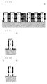
- FIGS. 2 , 3 , 4 , and 5 show a layout and cross-sectional structures of a semiconductor device according to the present invention.
- an output terminal wiring line 22 of an island-shaped semiconductor lower layer and a drain diffusion layer 23 are formed on a silicon oxide film 08 , an island-shaped semiconductor layer 24 is formed thereon, a source diffusion layer 25 is formed on the island-shaped semiconductor layer 24 , and a gate 26 is formed in a channel region of sidewalls sandwiched between the drain diffusion layer and the source diffusion layer through a gate insulating film, thereby forming an n-channel semiconductor device (an n-channel MOS transistor).
- island-shaped semiconductor lower portion wiring line 22 and drain diffusion layers 27 and 30 are formed on the silicon oxide film 08 , island-shaped semiconductor layers 28 and 31 are formed thereon, source diffusion layers 29 and 32 are formed on the island-shaped semiconductor layers 28 and 31 , the gate 26 is formed in a channel region of sidewalls sandwiched between each drain diffusion layer and each source diffusion layer through a gate insulating film, thereby forming p-channel semiconductor devices (p-channel MOS transistors).
- the two p-channel semiconductor devices and the one n-channel semiconductor device form a first inverter.
- a first power supply wiring line V SS 20 is formed on the source diffusion layers 12 and 25 of the n-channel semiconductor devices, and a second power supply wiring line V CC 33 is formed on the source diffusion layers 29 and 32 of the p-channel semiconductor devices in the first inverter.
- a second power supply wiring line V CC wiring line 21 is formed on the source diffusion layers 16 and 19 of the p-channel semiconductor devices in the second inverter.
- n CMOS inverters when the n CMOS inverters are aligned with respect to a substrate, it is preferable to arrange the p-channel MOS transistor of an n ⁇ 1th CMOS inverter and the p-channel MOS transistor of an nth CMOS inverter so as to be adjacent to each other and arrange the n-channel MOS transistor of the nth CMOS inverter and the n-channel MOS transistor of an n+1th CMOS inverter so as to be adjacent to each other.
- the two p-channel MOS transistors and the two n-channel transistors are arranged to be adjacent to each other, the first and second power supply wiring lines can be shortened, and resistances produced from the power supply wiring lines can be reduced.
- the p-channel MOS transistors and the n-channel MOS transistors may be counterchanged to constitute the plurality of inverters.
- the n CMOS inverters aligned with respect to the substrate may be arranged in m rows (m is two or above) with respect to the substrate.
- Phosphor is implanted based on, e.g., the ion implantation method to form n-type silicon 104 , 105 , 106 , and 107 ( FIG. 18 (X-X′), FIG. 19 (Y 1 -Y′ 1 ), FIG. 20 (Y 2 -Y′ 2 )).
- the polysilicon is etched ( FIG. 33 (X-X′), FIG. 34 (Y 1 -Y′ 1 ), FIG. 35 (Y 2 -Y′ 2 )).
- An oxide film 117 is deposited, flattened based on CMP, and then etched back ( FIG. 54 (X-X′), FIG. 55 (Y 1 -Y′ 1 ), FIG. 56 (Y 2 -Y′ 2 )).
- Oxidation is carried out to form gate insulating films 119 , 120 , 121 , 122 , 123 , and 124 ( FIG. 60 (X-X′), FIG. 61 (Y 1 -Y′ 1 ), FIG. 62 (Y 2 -Y′ 2 )).
- the nitride film, the polysilicon, and the nitride film are etched to form the input terminal lines, i.e., the gates 13 and 26 ( FIG. 72 (X-X′), FIG. 73 (Y 1 -Y′ 1 ), FIG. 74 (Y 2 -Y′ 2 )).
- An oxide film 127 is deposited, flattened based on CMP, and then etched back ( FIG. 78 (X-X′), FIG. 79 (Y 1 -Y′ 1 ), FIG. 80 (Y 2 -Y′ 2 )).
- Resists required to form a contact between the gates and the island-shaped semiconductor lower layer are formed ( FIG. 81 (X-X′), FIG. 82 (Y 1 -Y′ 1 ), FIG. 83 (Y 2 -Y′ 2 )).
- the oxide film is etched to form a contact 128 between the gates and the island-shaped semiconductor lower layer ( FIG. 84 (X-X′), FIG. 85 (Y 1 -Y′ 1 ), FIG. 86 (Y 2 -Y′ 2 )).
- FIG. 105 A resist required to form drain diffusion layers and source diffusion layers of p-channel semiconductor devices is formed ( FIG. 105 (X-X′), FIG. 106 (Y 1 -Y′ 1 ), FIG. 107 (Y 2 -Y′ 2 )).
- the oxide film is delaminated, and a heat process is carried out to ionize an impurity ( FIG. 111 (X-X′), FIG. 112 (Y 1 -Y′ 1 ), FIG. 113 (Y 2 -Y′ 2 )).
- An oxide film 130 is deposited, flattened based on CMP, and then etched back ( FIG. 126 (X-X′), FIG. 127 (Y 1 -Y′ 1 ), FIG. 128 (Y 2 -Y′ 2 )).
- Resists required to form contacts that connect the source diffusion layers 12 and 25 of the n-channel semiconductor devices with a first power supply wiring line V SS 20 and contacts that connect the source diffusion layers 29 and 32 of the p-channel semiconductor devices in a first inverter with a second power supply wiring line V CC 33 are formed, and resists required to form contacts that connect the source diffusion layers 16 and 19 of the p-channel semiconductor devices in a second inverter with a second power supply wiring line V CC 21 are formed ( FIG. 129 (X-X′), FIG. 130 (Y 1 -Y′ 1 ), FIG. 131 (Y 2 -Y′ 2 )).
- the oxide film is etched to form contacts 133 and 134 that connect the source diffusion layers 12 and 25 of the n-channel semiconductor devices with the first power supply wiring line V SS 20 , contacts 135 and 136 that connect the source diffusion layers 29 and 32 of the p-channel semiconductor devices in the first inverter with the second power supply wiring line V CC 33 , and contacts 132 and 131 that connect the source diffusion layers 16 and 19 of the p-channel semiconductor devices in the second inverter with the second power supply wiring line V CC 21 ( FIG. 132 (X-X′), FIG. 133 (Y 1 -Y′ 1 ), FIG. 134 (Y 2 -Y′ 2 )).
- the resists are delaminated ( FIG. 135 (X-X′), FIG. 136 (Y 1 -Y′ 1 ), FIG. 137 (Y 2 -Y′ 2 )).
- the metal is etched to form the first power supply wiring line V SS 20 and the second power supply wiring lines V CC 21 and 33 ( FIG. 144 (X-X′), FIG. 145 (Y 1 -Y′ 1 ), FIG. 146 (Y 2 -Y′ 2 )).
- the resists are delaminated ( FIG. 147 (X-X′), FIG. 148 (Y 1 -Y′ 1 ), FIG. 149 (Y 2 -Y′ 2 )).
- An oxide film 138 is deposited and flattened based on CMP ( FIG. 150 (X-X′), FIG. 151 (Y 1 -Y′ 1 ), FIG. 152 (Y 2 -Y′ 2 )).
- FIG. 153 shows a CMOS inverter coupling circuit in which CMOS inverters are arranged in three rows and two columns as a specific example of the circuits arranged in m rows (m is two or above). It is to be noted that an example where one CMOS inverter has two P-channel MOS transistors (p-channel semiconductor devices) in a column direction will be explained, but the number of the P-channel MOS transistors in the column direction of the CMOS inverter may be one.
- FIG. 154 is an X 1 -X′ 1 cross-sectional view
- FIG. 155 is an X 2 -X′ 2 cross-sectional view
- FIG. 156 is an X 3 -X′ 3 cross-sectional view
- FIG. 157 is a Y 1 -Y′ 1 cross-sectional view
- FIG. 158 is a Y 2 -Y′ 2 cross-sectional view.
- an output terminal wiring line 215 of an island-shaped semiconductor lower layer and a drain diffusion layer 216 are formed on a silicon oxide film 201 , an island-shaped semiconductor layer 217 is formed thereon, a source diffusion layer 218 is formed on the island-shaped semiconductor layer 217 , and a gate 219 is formed in a channel region of sidewalls sandwiched between the drain diffusion layer and the source diffusion layer through a gate insulating film, thereby forming an n-channel semiconductor device.
- the output terminal wiring line 215 of the island-shaped semiconductor lower layer and drain diffusion layers 220 and 223 are formed on the silicon oxide film 201 , island-shaped semiconductor layers 221 and 224 are formed thereon, source diffusion layers 222 and 225 are formed on the island-shaped semiconductor layers 221 and 224 , and the gate 219 is formed in the channel region of sidewalls sandwiched between the drain diffusion layers and the source diffusion layers through the gate insulating film, thereby forming p-channel semiconductor devices.
- the two p-channel semiconductor devices and the one n-channel semiconductor device form an inverter arranged in a third row and a second column.
- an output terminal wiring line 202 of the island-shaped semiconductor lower layer and a drain diffusion layer 203 are formed on the silicon oxide film 201 , an island-shaped semiconductor layer 204 is formed thereon, a source diffusion layer 205 is formed on the island-shaped semiconductor layer 204 , and a gate 206 is formed in a channel region of sidewalls sandwiched between the drain diffusion layer and the source diffusion layer through a gate insulating film, thereby forming an n-channel semiconductor device.
- an output terminal wiring line 315 of the island-shaped semiconductor lower layer and a drain diffusion layer 316 is formed on the silicon oxide film 201 , an island-shaped semiconductor layer 317 is formed thereon, a source diffusion layer 318 is formed on the island-shaped semiconductor layer 317 , and a gate 319 is formed in a channel region of sidewalls sandwiched between the drain diffusion layer and the source diffusion layer through a gate insulating film, thereby forming an n-channel semiconductor device.
- the output terminal wiring line 315 of the island-shaped semiconductor lower layer and drain diffusion layers 320 and 323 are formed on the silicon oxide film 201 , island-shaped semiconductor layers 321 and 324 are formed thereon, source diffusion layers 322 and 325 are formed on the island-shaped semiconductor layers 321 and 324 , and the gate 319 is formed in the channel region of sidewalls sandwiched between the drain diffusion layers and the source diffusion layers through the gate insulating film, thereby forming p-channel semiconductor device.
- the two p-channel semiconductor devices and the one n-channel semiconductor device form an inverter arranged in a second row and the second column.
- the output terminal wiring line 402 of the island-shaped semiconductor lower layer and drain diffusion layers 407 and 410 are formed on the silicon oxide film 201 , island-shaped semiconductor layers 408 and 411 are formed thereon, source diffusion layers 409 and 412 are formed on the island-shaped semiconductor layers 408 and 411 , and the gate 406 is formed in the channel region of sidewalls sandwiched between the drain diffusion layers and the source diffusion layers through the gate insulating film, thereby forming p-channel semiconductor devices.
- the two p-channel semiconductor devices and the one n-channel semiconductor device form an inverter arranged in the first row and the first column.
- the present invention has the first power supply wiring lines V SS and the second power supply wiring lines V CC supplied from upper sides of both the nMOS SGT and the pMOS SGT, and has:
- a metal wiring line connecting the respective contacts with each other is not required, thereby providing a semiconductor device formed of the highly integrated CMOS inverter coupling circuit using SGTs.
Landscapes
- Engineering & Computer Science (AREA)
- Power Engineering (AREA)
- Microelectronics & Electronic Packaging (AREA)
- General Physics & Mathematics (AREA)
- Condensed Matter Physics & Semiconductors (AREA)
- Computer Hardware Design (AREA)
- Physics & Mathematics (AREA)
- Manufacturing & Machinery (AREA)
- Metal-Oxide And Bipolar Metal-Oxide Semiconductor Integrated Circuits (AREA)
- Thin Film Transistor (AREA)
- Electrodes Of Semiconductors (AREA)
- Semiconductor Integrated Circuits (AREA)
- Logic Circuits (AREA)
Applications Claiming Priority (3)
| Application Number | Priority Date | Filing Date | Title |
|---|---|---|---|
| JP2007-143891 | 2007-05-30 | ||
| JP2007143891A JP5130596B2 (ja) | 2007-05-30 | 2007-05-30 | 半導体装置 |
| PCT/JP2008/052450 WO2008146505A1 (fr) | 2007-05-30 | 2008-02-14 | Dispositif à semi-conducteurs |
Related Parent Applications (1)
| Application Number | Title | Priority Date | Filing Date |
|---|---|---|---|
| PCT/JP2008/052450 Continuation WO2008146505A1 (fr) | 2007-05-30 | 2008-02-14 | Dispositif à semi-conducteurs |
Publications (2)
| Publication Number | Publication Date |
|---|---|
| US20090057722A1 US20090057722A1 (en) | 2009-03-05 |
| US8039893B2 true US8039893B2 (en) | 2011-10-18 |
Family
ID=40074778
Family Applications (1)
| Application Number | Title | Priority Date | Filing Date |
|---|---|---|---|
| US12/284,327 Active US8039893B2 (en) | 2007-05-30 | 2008-09-19 | CMOS inverter coupling circuit comprising vertical transistors |
Country Status (7)
| Country | Link |
|---|---|
| US (1) | US8039893B2 (fr) |
| EP (2) | EP2061075B1 (fr) |
| JP (1) | JP5130596B2 (fr) |
| KR (1) | KR101057438B1 (fr) |
| CN (1) | CN101542715B (fr) |
| TW (1) | TW200847397A (fr) |
| WO (1) | WO2008146505A1 (fr) |
Cited By (39)
| Publication number | Priority date | Publication date | Assignee | Title |
|---|---|---|---|---|
| US20100207201A1 (en) * | 2008-01-29 | 2010-08-19 | Fujio Masuoka | Semiconductor device and production method therefor |
| US20100264484A1 (en) * | 2009-04-17 | 2010-10-21 | Fujio Masuoka | Semiconductor device |
| US20100270611A1 (en) * | 2009-04-28 | 2010-10-28 | Fujio Masuoka | Semiconductor device including a mos transistor and production method therefor |
| US20100308422A1 (en) * | 2009-06-05 | 2010-12-09 | Unisantis Electronics (Japan) Ltd. | Semiconductor device |
| US20110062521A1 (en) * | 2009-09-16 | 2011-03-17 | Fujio Masuoka | Semiconductor device |
| US20110089496A1 (en) * | 2009-08-11 | 2011-04-21 | Unisantis Electronics (Japan) Ltd. | Semiconductor device and production method |
| US20110260259A1 (en) * | 2010-04-21 | 2011-10-27 | Fujio Masuoka | Semiconductor device |
| US8319293B2 (en) | 2009-03-25 | 2012-11-27 | Unisantis Electronics Singapore Pte Ltd. | Semiconductor device and production method therefor |
| US8482041B2 (en) | 2007-10-29 | 2013-07-09 | Unisantis Electronics Singapore Pte Ltd. | Semiconductor structure and method of fabricating the semiconductor structure |
| US8487357B2 (en) | 2010-03-12 | 2013-07-16 | Unisantis Electronics Singapore Pte Ltd. | Solid state imaging device having high sensitivity and high pixel density |
| US8486785B2 (en) | 2010-06-09 | 2013-07-16 | Unisantis Electronics Singapore Pte Ltd. | Surround gate CMOS semiconductor device |
| US8564034B2 (en) | 2011-09-08 | 2013-10-22 | Unisantis Electronics Singapore Pte. Ltd. | Solid-state imaging device |
| US8575662B2 (en) | 2010-03-08 | 2013-11-05 | Unisantis Electronics Singapore Pte Ltd. | Solid state imaging device having high pixel density |
| US8610202B2 (en) | 2009-10-01 | 2013-12-17 | Unisantis Electronics Singapore Pte Ltd. | Semiconductor device having a surrounding gate |
| US8669601B2 (en) | 2011-09-15 | 2014-03-11 | Unisantis Electronics Singapore Pte. Ltd. | Method for producing semiconductor device and semiconductor device having pillar-shaped semiconductor |
| US8748938B2 (en) | 2012-02-20 | 2014-06-10 | Unisantis Electronics Singapore Pte. Ltd. | Solid-state imaging device |
| US8772175B2 (en) | 2011-12-19 | 2014-07-08 | Unisantis Electronics Singapore Pte. Ltd. | Method for manufacturing semiconductor device and semiconductor device |
| US8916478B2 (en) | 2011-12-19 | 2014-12-23 | Unisantis Electronics Singapore Pte. Ltd. | Method for manufacturing semiconductor device and semiconductor device |
| US9117528B2 (en) | 2014-01-20 | 2015-08-25 | Unisantis Electronics Singapore Pte. Ltd. | Semiconductor device |
| US9153697B2 (en) | 2010-06-15 | 2015-10-06 | Unisantis Electronics Singapore Pte Ltd. | Surrounding gate transistor (SGT) structure |
| US20160042783A1 (en) * | 2013-10-23 | 2016-02-11 | Unisantis Electronics Singapore Pte. Ltd. | Semiconductor device with a plurality of surrounding gate transistors |
| US20160056173A1 (en) * | 2013-09-03 | 2016-02-25 | Unisantis Electronics Singapore Pte. Ltd. | Semiconductor device with surrounding gate transistors in a nand circuit |
| US20160155842A1 (en) * | 2014-11-27 | 2016-06-02 | Unisantis Electronics Singapore Pte. Ltd. | Pillar-shaped semiconductor device and method for producing the same |
| US9449988B2 (en) | 2013-08-08 | 2016-09-20 | Unisantis Electronics Singapore Pte. Ltd. | Semiconductor device with six transistors forming a nor circuit |
| US9484424B2 (en) | 2013-07-30 | 2016-11-01 | Unisantis Electronics Singapore Pte. Ltd. | Semiconductor device with a NAND circuit having four transistors |
| US9590631B2 (en) | 2014-04-22 | 2017-03-07 | Unisantis Electronics Singapore Pte. Ltd. | Semiconductor device |
| US9601510B2 (en) | 2013-08-08 | 2017-03-21 | Unisantis Electronics Singapore Pte. Ltd. | Semiconductor device with six transistors forming a NAND circuit |
| US9627496B2 (en) | 2013-07-30 | 2017-04-18 | Unisantis Electronics Singapore Pte. Ltd. | Semiconductor with a two-input NOR circuit |
| US9627407B2 (en) | 2014-04-22 | 2017-04-18 | Unisantis Electronics Singapore Pte. Ltd. | Semiconductor device comprising a NOR decoder with an inverter |
| US9646991B2 (en) | 2013-09-03 | 2017-05-09 | Unisantis Electronics Singapore Pte. Ltd. | Semiconductor device with surrounding gate transistors in a NOR circuit |
| US9666578B1 (en) | 2016-04-12 | 2017-05-30 | International Business Machines Corporation | Vertical FETs with high density capacitor |
| US20170365611A1 (en) * | 2016-06-20 | 2017-12-21 | Samsung Electronics Co., Ltd. | Semiconductor device |
| US9859421B1 (en) * | 2016-09-21 | 2018-01-02 | International Business Machines Corporation | Vertical field effect transistor with subway etch replacement metal gate |
| US9876015B1 (en) | 2017-02-16 | 2018-01-23 | International Business Machines Corporation | Tight pitch inverter using vertical transistors |
| US20180138093A1 (en) * | 2016-09-08 | 2018-05-17 | International Business Machines Corporation | Low resistance source-drain contacts using high temperature silicides |
| US10720364B2 (en) | 2018-08-20 | 2020-07-21 | International Business Machines Corporation | Forming vertical transistor devices with greater layout flexibility and packing density |
| US10944012B2 (en) | 2019-01-02 | 2021-03-09 | International Business Machines Corporation | Area-efficient inverter using stacked vertical transistors |
| US20210193834A1 (en) * | 2019-12-24 | 2021-06-24 | Samsung Electronics Co., Ltd. | Semiconductor devices |
| US11908907B2 (en) | 2020-12-11 | 2024-02-20 | International Business Machines Corporation | VFET contact formation |
Families Citing this family (50)
| Publication number | Priority date | Publication date | Assignee | Title |
|---|---|---|---|---|
| JP5122212B2 (ja) * | 2007-08-02 | 2013-01-16 | ユニサンティス エレクトロニクス シンガポール プライベート リミテッド | 半導体装置 |
| KR100946084B1 (ko) * | 2008-03-27 | 2010-03-10 | 주식회사 하이닉스반도체 | 반도체 소자의 수직형 트랜지스터 및 그 형성방법 |
| JP5323610B2 (ja) * | 2009-08-18 | 2013-10-23 | ユニサンティス エレクトロニクス シンガポール プライベート リミテッド | 半導体装置とその製造方法 |
| JP5006375B2 (ja) * | 2009-12-10 | 2012-08-22 | ユニサンティス エレクトロニクス シンガポール プライベート リミテッド | 半導体装置及びその製造方法 |
| KR101723864B1 (ko) * | 2010-10-08 | 2017-04-07 | 삼성전자주식회사 | 수직 채널 트랜지스터를 구비하는 반도체 장치 및 그 제조 방법 |
| US8598633B2 (en) * | 2012-01-16 | 2013-12-03 | GlobalFoundries, Inc. | Semiconductor device having contact layer providing electrical connections |
| CN103531635B (zh) * | 2013-09-18 | 2016-03-16 | 北京大学 | 一种基于纳米线的立式环栅晶体管及其制备方法 |
| US9373623B2 (en) * | 2013-12-20 | 2016-06-21 | Taiwan Semiconductor Manufacturing Company Limited | Multi-layer semiconductor structures for fabricating inverter chains |
| WO2015155863A1 (fr) | 2014-04-10 | 2015-10-15 | ユニサンティス エレクトロニクス シンガポール プライベート リミテッド | Dispositif à semi-conducteur |
| WO2015155862A1 (fr) | 2014-04-10 | 2015-10-15 | ユニサンティス エレクトロニクス シンガポール プライベート リミテッド | Dispositif à semi-conducteurs |
| US9755033B2 (en) | 2014-06-13 | 2017-09-05 | Taiwan Semiconductor Manufacturing Co., Ltd. | Semiconductor device and method of forming vertical structure |
| EP3158588A4 (fr) * | 2014-06-23 | 2018-01-17 | Intel Corporation | Techniques de formation d'architectures de transistor verticales |
| US9490331B2 (en) * | 2014-06-30 | 2016-11-08 | Taiwan Semiconductor Manufacturing Company Limited | Formation of semiconductor arrangement comprising buffer layer and semiconductor column overlying buffer layer |
| JP5990843B2 (ja) | 2014-07-14 | 2016-09-14 | ユニサンティス エレクトロニクス シンガポール プライベート リミテッドUnisantis Electronics Singapore Pte Ltd. | 半導体装置の製造方法、及び、半導体装置 |
| JP5928658B1 (ja) | 2014-08-07 | 2016-06-01 | ユニサンティス エレクトロニクス シンガポール プライベート リミテッドUnisantis Electronics Singapore Pte Ltd. | 半導体装置の製造方法、及び、半導体装置 |
| US9673054B2 (en) * | 2014-08-18 | 2017-06-06 | Micron Technology, Inc. | Array of gated devices and methods of forming an array of gated devices |
| WO2016031014A1 (fr) | 2014-08-28 | 2016-03-03 | ユニサンティス エレクトロニクス シンガポール プライベート リミテッド | Dispositif à semi-conducteur et procédé de fabrication de dispositif à semi-conducteur |
| WO2016035213A1 (fr) | 2014-09-05 | 2016-03-10 | ユニサンティス エレクトロニクス シンガポール プライベート リミテッド | Dispositif à semiconducteurs |
| KR101743864B1 (ko) | 2015-01-28 | 2017-06-07 | 허천신 | 수직형 씨모스 인버터 소자 |
| WO2016139755A1 (fr) | 2015-03-03 | 2016-09-09 | ユニサンティス エレクトロニクス シンガポール プライベート リミテッド | Dispositif à semi-conducteurs |
| US9842651B2 (en) | 2015-11-25 | 2017-12-12 | Sunrise Memory Corporation | Three-dimensional vertical NOR flash thin film transistor strings |
| US9892800B2 (en) | 2015-09-30 | 2018-02-13 | Sunrise Memory Corporation | Multi-gate NOR flash thin-film transistor strings arranged in stacked horizontal active strips with vertical control gates |
| US11120884B2 (en) | 2015-09-30 | 2021-09-14 | Sunrise Memory Corporation | Implementing logic function and generating analog signals using NOR memory strings |
| US10121553B2 (en) | 2015-09-30 | 2018-11-06 | Sunrise Memory Corporation | Capacitive-coupled non-volatile thin-film transistor NOR strings in three-dimensional arrays |
| US10692874B2 (en) | 2017-06-20 | 2020-06-23 | Sunrise Memory Corporation | 3-dimensional NOR string arrays in segmented stacks |
| JP7203054B2 (ja) | 2017-06-20 | 2023-01-12 | サンライズ メモリー コーポレイション | 3次元nor型メモリアレイアーキテクチャ及びその製造方法 |
| US10608008B2 (en) | 2017-06-20 | 2020-03-31 | Sunrise Memory Corporation | 3-dimensional nor strings with segmented shared source regions |
| US10290639B2 (en) * | 2017-09-12 | 2019-05-14 | Globalfoundries Inc. | VNW SRAM with trinity cross-couple PD/PU contact and method for producing the same |
| US10366983B2 (en) * | 2017-12-29 | 2019-07-30 | Micron Technology, Inc. | Semiconductor devices including control logic structures, electronic systems, and related methods |
| US10340267B1 (en) * | 2017-12-29 | 2019-07-02 | Micron Technology, Inc. | Semiconductor devices including control logic levels, and related memory devices, control logic assemblies, electronic systems, and methods |
| US10297290B1 (en) * | 2017-12-29 | 2019-05-21 | Micron Technology, Inc. | Semiconductor devices, and related control logic assemblies, control logic devices, electronic systems, and methods |
| US10475812B2 (en) | 2018-02-02 | 2019-11-12 | Sunrise Memory Corporation | Three-dimensional vertical NOR flash thin-film transistor strings |
| CN112567516A (zh) | 2018-07-12 | 2021-03-26 | 日升存储公司 | 三维nor存储器阵列的制造方法 |
| US11069696B2 (en) * | 2018-07-12 | 2021-07-20 | Sunrise Memory Corporation | Device structure for a 3-dimensional NOR memory array and methods for improved erase operations applied thereto |
| US11751391B2 (en) | 2018-07-12 | 2023-09-05 | Sunrise Memory Corporation | Methods for fabricating a 3-dimensional memory structure of nor memory strings |
| TWI713195B (zh) | 2018-09-24 | 2020-12-11 | 美商森恩萊斯記憶體公司 | 三維nor記憶電路製程中之晶圓接合及其形成之積體電路 |
| EP3891780A4 (fr) | 2018-12-07 | 2022-12-21 | Sunrise Memory Corporation | Procédés de formation de réseaux de chaînes de mémoire de type nor verticales multicouches |
| US11670620B2 (en) | 2019-01-30 | 2023-06-06 | Sunrise Memory Corporation | Device with embedded high-bandwidth, high-capacity memory using wafer bonding |
| CN113424319A (zh) | 2019-02-11 | 2021-09-21 | 日升存储公司 | 垂直薄膜晶体管以及作为用于三维存储器阵列的位线连接器的应用 |
| US11515309B2 (en) | 2019-12-19 | 2022-11-29 | Sunrise Memory Corporation | Process for preparing a channel region of a thin-film transistor in a 3-dimensional thin-film transistor array |
| US11675500B2 (en) | 2020-02-07 | 2023-06-13 | Sunrise Memory Corporation | High capacity memory circuit with low effective latency |
| US11561911B2 (en) | 2020-02-24 | 2023-01-24 | Sunrise Memory Corporation | Channel controller for shared memory access |
| US11507301B2 (en) | 2020-02-24 | 2022-11-22 | Sunrise Memory Corporation | Memory module implementing memory centric architecture |
| US11705496B2 (en) | 2020-04-08 | 2023-07-18 | Sunrise Memory Corporation | Charge-trapping layer with optimized number of charge-trapping sites for fast program and erase of a memory cell in a 3-dimensional NOR memory string array |
| US11937424B2 (en) | 2020-08-31 | 2024-03-19 | Sunrise Memory Corporation | Thin-film storage transistors in a 3-dimensional array of nor memory strings and process for fabricating the same |
| US11842777B2 (en) | 2020-11-17 | 2023-12-12 | Sunrise Memory Corporation | Methods for reducing disturb errors by refreshing data alongside programming or erase operations |
| US11848056B2 (en) | 2020-12-08 | 2023-12-19 | Sunrise Memory Corporation | Quasi-volatile memory with enhanced sense amplifier operation |
| CN113299761A (zh) * | 2021-05-12 | 2021-08-24 | 深圳市华星光电半导体显示技术有限公司 | 阵列基板及其制备方法、显示面板 |
| TW202310429A (zh) | 2021-07-16 | 2023-03-01 | 美商日升存儲公司 | 薄膜鐵電電晶體的三維記憶體串陣列 |
| CN117712147A (zh) * | 2022-09-07 | 2024-03-15 | 长鑫存储技术有限公司 | 半导体结构及其形成方法、版图结构 |
Citations (12)
| Publication number | Priority date | Publication date | Assignee | Title |
|---|---|---|---|---|
| US4740826A (en) * | 1985-09-25 | 1988-04-26 | Texas Instruments Incorporated | Vertical inverter |
| JPH0271556A (ja) | 1988-09-06 | 1990-03-12 | Toshiba Corp | 半導体装置 |
| JPH02188966A (ja) | 1989-01-17 | 1990-07-25 | Toshiba Corp | Mos型半導体装置 |
| JPH03145761A (ja) | 1989-11-01 | 1991-06-20 | Toshiba Corp | 半導体装置 |
| US5208172A (en) * | 1992-03-02 | 1993-05-04 | Motorola, Inc. | Method for forming a raised vertical transistor |
| US5258635A (en) | 1988-09-06 | 1993-11-02 | Kabushiki Kaisha Toshiba | MOS-type semiconductor integrated circuit device |
| US6448953B1 (en) * | 1999-02-23 | 2002-09-10 | Seiko Epson Corporation | Driving circuit for electrooptical device, electrooptical device, and electronic apparatus |
| JP2004165297A (ja) | 2002-11-11 | 2004-06-10 | Fujitsu Ltd | 半導体装置 |
| US20040173844A1 (en) | 2003-03-05 | 2004-09-09 | Advanced Analogic Technologies, Inc. Advanced Analogic Technologies (Hongkong) Limited | Trench power MOSFET with planarized gate bus |
| JP2004356314A (ja) | 2003-05-28 | 2004-12-16 | Fujio Masuoka | 半導体装置 |
| JP2005268438A (ja) | 2004-03-17 | 2005-09-29 | Sharp Corp | 電界効果トランジスタおよびその作製方法 |
| US20060028861A1 (en) * | 2004-08-04 | 2006-02-09 | Gong-Heum Han | Semiconductor memory device and method for arranging and manufacturing the same |
Family Cites Families (9)
| Publication number | Priority date | Publication date | Assignee | Title |
|---|---|---|---|---|
| JPS6113661A (ja) * | 1984-06-29 | 1986-01-21 | Nippon Telegr & Teleph Corp <Ntt> | 半導体装置およびその製造方法 |
| JP3403231B2 (ja) * | 1993-05-12 | 2003-05-06 | 三菱電機株式会社 | 半導体装置およびその製造方法 |
| DE19781675B4 (de) * | 1996-03-28 | 2006-08-24 | Intel Corporation, Santa Clara | Speicherzellengestaltung mit vertikal gestapelten Überkeuzungen |
| KR20010056494A (ko) * | 1999-12-15 | 2001-07-04 | 윤종용 | 반도체 메모리 장치의 주변회로 레이아웃 방법 |
| TW541627B (en) * | 2001-03-26 | 2003-07-11 | Halo Lsi Inc | Stitch and select implementation in twin monos array |
| US7138685B2 (en) * | 2002-12-11 | 2006-11-21 | International Business Machines Corporation | Vertical MOSFET SRAM cell |
| JP2005310921A (ja) * | 2004-04-19 | 2005-11-04 | Okayama Prefecture | Mos型半導体装置及びその製造方法 |
| US20060261406A1 (en) * | 2005-05-18 | 2006-11-23 | Yijian Chen | Vertical integrated-gate CMOS device and its fabrication process |
| JP5114968B2 (ja) * | 2007-02-20 | 2013-01-09 | 富士通セミコンダクター株式会社 | 半導体装置及びその製造方法 |
-
2007
- 2007-05-30 JP JP2007143891A patent/JP5130596B2/ja active Active
-
2008
- 2008-02-14 WO PCT/JP2008/052450 patent/WO2008146505A1/fr active Application Filing
- 2008-02-14 KR KR1020087030390A patent/KR101057438B1/ko active IP Right Grant
- 2008-02-14 EP EP08711292.6A patent/EP2061075B1/fr active Active
- 2008-02-14 CN CN2008800004151A patent/CN101542715B/zh active Active
- 2008-02-14 EP EP13174146.4A patent/EP2645411A3/fr not_active Withdrawn
- 2008-03-25 TW TW097110485A patent/TW200847397A/zh unknown
- 2008-09-19 US US12/284,327 patent/US8039893B2/en active Active
Patent Citations (14)
| Publication number | Priority date | Publication date | Assignee | Title |
|---|---|---|---|---|
| US4740826A (en) * | 1985-09-25 | 1988-04-26 | Texas Instruments Incorporated | Vertical inverter |
| JPH0271556A (ja) | 1988-09-06 | 1990-03-12 | Toshiba Corp | 半導体装置 |
| US5258635A (en) | 1988-09-06 | 1993-11-02 | Kabushiki Kaisha Toshiba | MOS-type semiconductor integrated circuit device |
| JPH02188966A (ja) | 1989-01-17 | 1990-07-25 | Toshiba Corp | Mos型半導体装置 |
| JPH03145761A (ja) | 1989-11-01 | 1991-06-20 | Toshiba Corp | 半導体装置 |
| US5208172A (en) * | 1992-03-02 | 1993-05-04 | Motorola, Inc. | Method for forming a raised vertical transistor |
| US6448953B1 (en) * | 1999-02-23 | 2002-09-10 | Seiko Epson Corporation | Driving circuit for electrooptical device, electrooptical device, and electronic apparatus |
| JP2004165297A (ja) | 2002-11-11 | 2004-06-10 | Fujitsu Ltd | 半導体装置 |
| US20040173844A1 (en) | 2003-03-05 | 2004-09-09 | Advanced Analogic Technologies, Inc. Advanced Analogic Technologies (Hongkong) Limited | Trench power MOSFET with planarized gate bus |
| CN1757117A (zh) | 2003-03-05 | 2006-04-05 | 先进模拟科技公司 | 具有平坦化的栅极总线的沟槽功率金属氧化物半导体场效应晶体管 |
| JP2004356314A (ja) | 2003-05-28 | 2004-12-16 | Fujio Masuoka | 半導体装置 |
| US20040262681A1 (en) | 2003-05-28 | 2004-12-30 | Fujio Masuoka | Semiconductor device |
| JP2005268438A (ja) | 2004-03-17 | 2005-09-29 | Sharp Corp | 電界効果トランジスタおよびその作製方法 |
| US20060028861A1 (en) * | 2004-08-04 | 2006-02-09 | Gong-Heum Han | Semiconductor memory device and method for arranging and manufacturing the same |
Non-Patent Citations (4)
| Title |
|---|
| Claim recitation for U.S. Appl. No. 12/697,683, filed Feb. 1, 2010. * |
| Iwai, Makoto et al., "High-Performance Buried-Gate Surrounding Gate Transistor for Future Three-Dimensional Devices," Japanese Journal of Applied Physics, vol. 43, No. 10, 2004, pp. 6904-6906. |
| Watanebe, et al, "A Novel Circuit Technology with Surrounding Gate Transistors (SGT's) for Ultra High Density DRAM's", IEEE Journal of Solid-State Circuits, vol. 30, No. 9, pp. 960-971, 1995. |
| Written Opinion of the International Search Authority issued May 9, 2008 in International application No. PCT/JP2008/052450. |
Cited By (66)
| Publication number | Priority date | Publication date | Assignee | Title |
|---|---|---|---|---|
| US8482041B2 (en) | 2007-10-29 | 2013-07-09 | Unisantis Electronics Singapore Pte Ltd. | Semiconductor structure and method of fabricating the semiconductor structure |
| US20100207201A1 (en) * | 2008-01-29 | 2010-08-19 | Fujio Masuoka | Semiconductor device and production method therefor |
| US8598650B2 (en) | 2008-01-29 | 2013-12-03 | Unisantis Electronics Singapore Pte Ltd. | Semiconductor device and production method therefor |
| US8319293B2 (en) | 2009-03-25 | 2012-11-27 | Unisantis Electronics Singapore Pte Ltd. | Semiconductor device and production method therefor |
| US8642426B2 (en) | 2009-03-25 | 2014-02-04 | Unisantis Electronics Singapore Pte Ltd. | Semiconductor device and production method therefor |
| US8212311B2 (en) * | 2009-04-17 | 2012-07-03 | Unisantis Electronics Singapore Pte Ltd. | Semiconductor device having increased gate length implemented by surround gate transistor arrangements |
| US20100264484A1 (en) * | 2009-04-17 | 2010-10-21 | Fujio Masuoka | Semiconductor device |
| US8647947B2 (en) | 2009-04-28 | 2014-02-11 | Unisantis Electronics Singapore Pte Ltd. | Semiconductor device including a MOS transistor and production method therefor |
| US20100270611A1 (en) * | 2009-04-28 | 2010-10-28 | Fujio Masuoka | Semiconductor device including a mos transistor and production method therefor |
| US8497548B2 (en) | 2009-04-28 | 2013-07-30 | Unisantis Electronics Singapore Pte Ltd. | Semiconductor device including a MOS transistor and production method therefor |
| US20100308422A1 (en) * | 2009-06-05 | 2010-12-09 | Unisantis Electronics (Japan) Ltd. | Semiconductor device |
| US8772881B2 (en) | 2009-06-05 | 2014-07-08 | Unisantis Electronics Singapore Pte Ltd. | Semiconductor device |
| US9059309B2 (en) | 2009-08-11 | 2015-06-16 | Unisantis Electronics Singapore Pte Ltd. | Semiconductor device and production method |
| US20110089496A1 (en) * | 2009-08-11 | 2011-04-21 | Unisantis Electronics (Japan) Ltd. | Semiconductor device and production method |
| US9484268B2 (en) | 2009-08-11 | 2016-11-01 | Unisantis Electronics Singapore Pte Ltd. | Semiconductor device and production method |
| US8558317B2 (en) | 2009-08-11 | 2013-10-15 | Unisantis Electronics Singapore Pte Ltd. | Semiconductor device and production method |
| US20110062521A1 (en) * | 2009-09-16 | 2011-03-17 | Fujio Masuoka | Semiconductor device |
| US8441066B2 (en) | 2009-09-16 | 2013-05-14 | Unisantis Electronics Singapore Pte Ltd. | Semiconductor device |
| US8610202B2 (en) | 2009-10-01 | 2013-12-17 | Unisantis Electronics Singapore Pte Ltd. | Semiconductor device having a surrounding gate |
| US8575662B2 (en) | 2010-03-08 | 2013-11-05 | Unisantis Electronics Singapore Pte Ltd. | Solid state imaging device having high pixel density |
| US8487357B2 (en) | 2010-03-12 | 2013-07-16 | Unisantis Electronics Singapore Pte Ltd. | Solid state imaging device having high sensitivity and high pixel density |
| US20110260259A1 (en) * | 2010-04-21 | 2011-10-27 | Fujio Masuoka | Semiconductor device |
| US8319288B2 (en) * | 2010-04-21 | 2012-11-27 | Unisantis Electronics Singapore Pte Ltd. | Semiconductor device |
| US8609494B2 (en) | 2010-06-09 | 2013-12-17 | Unisantis Electronics Singapore Pte Ltd. | Surround gate CMOS semiconductor device |
| US8486785B2 (en) | 2010-06-09 | 2013-07-16 | Unisantis Electronics Singapore Pte Ltd. | Surround gate CMOS semiconductor device |
| US9153697B2 (en) | 2010-06-15 | 2015-10-06 | Unisantis Electronics Singapore Pte Ltd. | Surrounding gate transistor (SGT) structure |
| US8564034B2 (en) | 2011-09-08 | 2013-10-22 | Unisantis Electronics Singapore Pte. Ltd. | Solid-state imaging device |
| US8669601B2 (en) | 2011-09-15 | 2014-03-11 | Unisantis Electronics Singapore Pte. Ltd. | Method for producing semiconductor device and semiconductor device having pillar-shaped semiconductor |
| US9245889B2 (en) | 2011-12-19 | 2016-01-26 | Unisantis Electronics Singapore Pte. Ltd. | Method for manufacturing semiconductor device and semiconductor device |
| US9748244B2 (en) | 2011-12-19 | 2017-08-29 | Unisantis Electronics Singapore Pte. Ltd. | Method for manufacturing semiconductor device and semiconductor device |
| US8916478B2 (en) | 2011-12-19 | 2014-12-23 | Unisantis Electronics Singapore Pte. Ltd. | Method for manufacturing semiconductor device and semiconductor device |
| US8772175B2 (en) | 2011-12-19 | 2014-07-08 | Unisantis Electronics Singapore Pte. Ltd. | Method for manufacturing semiconductor device and semiconductor device |
| US9035384B2 (en) | 2011-12-19 | 2015-05-19 | Unisantis Electronics Singapore Pte. Ltd. | Semiconductor device |
| US9806163B2 (en) | 2011-12-19 | 2017-10-31 | Unisantis Electronics Singapore Pte. Ltd. | Semiconductor device having an nMOS SGT and a pMOS SGT |
| US9362353B2 (en) | 2011-12-19 | 2016-06-07 | Unisantis Electronics Singapore Pte. Ltd. | Semiconductor device |
| US9478545B2 (en) | 2011-12-19 | 2016-10-25 | Unisantis Electronics Singapore Pte. Ltd. | Method for manufacturing semiconductor device and semiconductor device |
| US8748938B2 (en) | 2012-02-20 | 2014-06-10 | Unisantis Electronics Singapore Pte. Ltd. | Solid-state imaging device |
| US9627496B2 (en) | 2013-07-30 | 2017-04-18 | Unisantis Electronics Singapore Pte. Ltd. | Semiconductor with a two-input NOR circuit |
| US9484424B2 (en) | 2013-07-30 | 2016-11-01 | Unisantis Electronics Singapore Pte. Ltd. | Semiconductor device with a NAND circuit having four transistors |
| US9601510B2 (en) | 2013-08-08 | 2017-03-21 | Unisantis Electronics Singapore Pte. Ltd. | Semiconductor device with six transistors forming a NAND circuit |
| US9449988B2 (en) | 2013-08-08 | 2016-09-20 | Unisantis Electronics Singapore Pte. Ltd. | Semiconductor device with six transistors forming a nor circuit |
| US20160056173A1 (en) * | 2013-09-03 | 2016-02-25 | Unisantis Electronics Singapore Pte. Ltd. | Semiconductor device with surrounding gate transistors in a nand circuit |
| US9646991B2 (en) | 2013-09-03 | 2017-05-09 | Unisantis Electronics Singapore Pte. Ltd. | Semiconductor device with surrounding gate transistors in a NOR circuit |
| US9716092B2 (en) | 2013-09-03 | 2017-07-25 | Unisantis Electronics Singapore Pte. Ltd. | Semiconductor device with surrounding gate transistors in a NAND circuit |
| US10910039B2 (en) | 2013-10-23 | 2021-02-02 | Unisantis Electronics Singapore Pte. Ltd. | Semiconductor device with a plurality of surrounding gate transistors |
| US10311945B2 (en) * | 2013-10-23 | 2019-06-04 | Unisantis Electronics Singapore Pte. Ltd. | Semiconductor device with a plurality of surrounding gate transistors |
| US20160042783A1 (en) * | 2013-10-23 | 2016-02-11 | Unisantis Electronics Singapore Pte. Ltd. | Semiconductor device with a plurality of surrounding gate transistors |
| US9117528B2 (en) | 2014-01-20 | 2015-08-25 | Unisantis Electronics Singapore Pte. Ltd. | Semiconductor device |
| US9590631B2 (en) | 2014-04-22 | 2017-03-07 | Unisantis Electronics Singapore Pte. Ltd. | Semiconductor device |
| US9627407B2 (en) | 2014-04-22 | 2017-04-18 | Unisantis Electronics Singapore Pte. Ltd. | Semiconductor device comprising a NOR decoder with an inverter |
| US9673321B2 (en) * | 2014-11-27 | 2017-06-06 | Unisantis Electronics Singapore Pte. Ltd. | Pillar-shaped semiconductor device and method for producing the same |
| US20160155842A1 (en) * | 2014-11-27 | 2016-06-02 | Unisantis Electronics Singapore Pte. Ltd. | Pillar-shaped semiconductor device and method for producing the same |
| US10050124B2 (en) | 2014-11-27 | 2018-08-14 | Unisantis Electronics Singapore Pte. Ltd. | Method for producing a pillar-shaped semiconductor device |
| US9666578B1 (en) | 2016-04-12 | 2017-05-30 | International Business Machines Corporation | Vertical FETs with high density capacitor |
| US10128254B2 (en) * | 2016-06-20 | 2018-11-13 | Samsung Electronics Co., Ltd. | Semiconductor device |
| US20170365611A1 (en) * | 2016-06-20 | 2017-12-21 | Samsung Electronics Co., Ltd. | Semiconductor device |
| US20180138093A1 (en) * | 2016-09-08 | 2018-05-17 | International Business Machines Corporation | Low resistance source-drain contacts using high temperature silicides |
| US11062956B2 (en) * | 2016-09-08 | 2021-07-13 | International Business Machines Corporation | Low resistance source-drain contacts using high temperature silicides |
| US9859421B1 (en) * | 2016-09-21 | 2018-01-02 | International Business Machines Corporation | Vertical field effect transistor with subway etch replacement metal gate |
| US10141309B2 (en) | 2017-02-16 | 2018-11-27 | International Business Machines Corporation | Tight pitch inverter using vertical transistors |
| US9876015B1 (en) | 2017-02-16 | 2018-01-23 | International Business Machines Corporation | Tight pitch inverter using vertical transistors |
| US10720364B2 (en) | 2018-08-20 | 2020-07-21 | International Business Machines Corporation | Forming vertical transistor devices with greater layout flexibility and packing density |
| US10944012B2 (en) | 2019-01-02 | 2021-03-09 | International Business Machines Corporation | Area-efficient inverter using stacked vertical transistors |
| US20210193834A1 (en) * | 2019-12-24 | 2021-06-24 | Samsung Electronics Co., Ltd. | Semiconductor devices |
| US11769830B2 (en) * | 2019-12-24 | 2023-09-26 | Samsung Electronics Co., Ltd. | Semiconductor devices |
| US11908907B2 (en) | 2020-12-11 | 2024-02-20 | International Business Machines Corporation | VFET contact formation |
Also Published As
| Publication number | Publication date |
|---|---|
| EP2061075A1 (fr) | 2009-05-20 |
| EP2061075B1 (fr) | 2013-10-09 |
| US20090057722A1 (en) | 2009-03-05 |
| KR101057438B1 (ko) | 2011-08-17 |
| KR20090025236A (ko) | 2009-03-10 |
| WO2008146505A1 (fr) | 2008-12-04 |
| CN101542715A (zh) | 2009-09-23 |
| EP2061075A4 (fr) | 2012-06-13 |
| EP2645411A2 (fr) | 2013-10-02 |
| JP2008300558A (ja) | 2008-12-11 |
| EP2645411A3 (fr) | 2013-12-04 |
| JP5130596B2 (ja) | 2013-01-30 |
| CN101542715B (zh) | 2011-08-31 |
| TW200847397A (en) | 2008-12-01 |
Similar Documents
| Publication | Publication Date | Title |
|---|---|---|
| US8039893B2 (en) | CMOS inverter coupling circuit comprising vertical transistors | |
| JP5122212B2 (ja) | 半導体装置 | |
| US8212311B2 (en) | Semiconductor device having increased gate length implemented by surround gate transistor arrangements | |
| US11735479B2 (en) | Assemblies containing PMOS decks vertically-integrated with NMOS decks, and methods of forming integrated assemblies | |
| US8319288B2 (en) | Semiconductor device | |
| US8772881B2 (en) | Semiconductor device | |
| US8441066B2 (en) | Semiconductor device | |
| WO2011121738A1 (fr) | Dispositif semi-conducteur et procédé de fabrication de celui-ci | |
| JP2011216657A (ja) | 半導体装置 | |
| US20070241400A1 (en) | Semiconductor device | |
| US10032779B2 (en) | Semiconductor device with plasma damage protecting elements | |
| JP2005101217A (ja) | スタティックランダムアクセスメモリ | |
| CN107026158B (zh) | 基于沟槽的电荷泵装置 | |
| US20050205938A1 (en) | Semiconductor device and method of manufacture the same | |
| US8664063B2 (en) | Method of producing a semiconductor device and semiconductor device | |
| US6849904B2 (en) | Efficient source diffusion interconnect, MOS transistor and standard cell layout utilizing same | |
| JPH01235369A (ja) | 半導体集積回路装置 | |
| JP2007311694A (ja) | 半導体装置 |
Legal Events
| Date | Code | Title | Description |
|---|---|---|---|
| AS | Assignment |
Owner name: UNISANTIS ELECTRONICS (JAPAN) LTD., JAPAN Free format text: ASSIGNMENT OF ASSIGNORS INTEREST;ASSIGNORS:MASUOKA, FUJIO;NAKAMURA, HIROKI;REEL/FRAME:021644/0184 Effective date: 20080812 Owner name: TOHOKU UNIVERSITY, JAPAN Free format text: ASSIGNMENT OF ASSIGNORS INTEREST;ASSIGNORS:MASUOKA, FUJIO;NAKAMURA, HIROKI;REEL/FRAME:021644/0184 Effective date: 20080812 |
|
| AS | Assignment |
Owner name: UNISANTIS ELECTRONICS SINGAPORE PTE LTD., SINGAPOR Free format text: ASSIGNMENT OF ASSIGNORS INTEREST;ASSIGNOR:UNISANTIS ELECTRONICS JAPAN LTD.;REEL/FRAME:026968/0968 Effective date: 20110913 |
|
| STCF | Information on status: patent grant |
Free format text: PATENTED CASE |
|
| CC | Certificate of correction | ||
| FEPP | Fee payment procedure |
Free format text: PAYOR NUMBER ASSIGNED (ORIGINAL EVENT CODE: ASPN); ENTITY STATUS OF PATENT OWNER: SMALL ENTITY |
|
| FPAY | Fee payment |
Year of fee payment: 4 |
|
| MAFP | Maintenance fee payment |
Free format text: PAYMENT OF MAINTENANCE FEE, 8TH YR, SMALL ENTITY (ORIGINAL EVENT CODE: M2552); ENTITY STATUS OF PATENT OWNER: SMALL ENTITY Year of fee payment: 8 |
|
| MAFP | Maintenance fee payment |
Free format text: PAYMENT OF MAINTENANCE FEE, 12TH YR, SMALL ENTITY (ORIGINAL EVENT CODE: M2553); ENTITY STATUS OF PATENT OWNER: SMALL ENTITY Year of fee payment: 12 |