US7856330B2 - Measuring apparatus, testing apparatus, and electronic device - Google Patents
Measuring apparatus, testing apparatus, and electronic device Download PDFInfo
- Publication number
- US7856330B2 US7856330B2 US11/623,101 US62310107A US7856330B2 US 7856330 B2 US7856330 B2 US 7856330B2 US 62310107 A US62310107 A US 62310107A US 7856330 B2 US7856330 B2 US 7856330B2
- Authority
- US
- United States
- Prior art keywords
- signal
- test
- under
- section
- measuring apparatus
- Prior art date
- Legal status (The legal status is an assumption and is not a legal conclusion. Google has not performed a legal analysis and makes no representation as to the accuracy of the status listed.)
- Expired - Fee Related, expires
Links
Images

Classifications
-
- G—PHYSICS
- G01—MEASURING; TESTING
- G01R—MEASURING ELECTRIC VARIABLES; MEASURING MAGNETIC VARIABLES
- G01R31/00—Arrangements for testing electric properties; Arrangements for locating electric faults; Arrangements for electrical testing characterised by what is being tested not provided for elsewhere
- G01R31/28—Testing of electronic circuits, e.g. by signal tracer
- G01R31/317—Testing of digital circuits
- G01R31/31725—Timing aspects, e.g. clock distribution, skew, propagation delay
-
- G—PHYSICS
- G01—MEASURING; TESTING
- G01R—MEASURING ELECTRIC VARIABLES; MEASURING MAGNETIC VARIABLES
- G01R31/00—Arrangements for testing electric properties; Arrangements for locating electric faults; Arrangements for electrical testing characterised by what is being tested not provided for elsewhere
- G01R31/28—Testing of electronic circuits, e.g. by signal tracer
- G01R31/317—Testing of digital circuits
- G01R31/3181—Functional testing
- G01R31/319—Tester hardware, i.e. output processing circuits
- G01R31/3193—Tester hardware, i.e. output processing circuits with comparison between actual response and known fault free response
- G01R31/31937—Timing aspects, e.g. measuring propagation delay
Definitions
- a testing apparatus detects a data pattern of the signal-under-test by comparing a voltage values of the signal-under-test outputted out of the electronic device with threshold voltage when a predetermined test pattern is inputted to the electronic device. Then, it judges whether or not the data pattern coincides with the pattern of the expected values.
- a tenth aspect of the present invention provides a measuring apparatus that measures signal-under-test of which signal level is changed at a predetermined bit time interval.
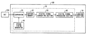
- the measuring apparatus includes: a strobe timing generator that sequentially generates strobes arranged at substantially even time intervals; a level comparison section that detects the level of the signal-under-test at a timing at which each strobe is sequentially provided; a capture memory that stores therein the signal level outputted by the level comparison section; and a digital signal processing section that calculates a comparison result indicating whether each logical value of data series including data which have substantially even time intervals and each of which interval is larger than a bit time interval of the signal-under-test is corresponding to an expected logical value and calculates a measurement result of the signal-under-test based on the comparison result.
- a judging section that judges the pass/fail result for the device under test based on the signal-under-test measured by the measuring apparatus.
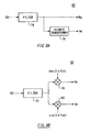
- FIGS. 5A and 5B are diagrams showing exemplary configurations of a digital signal processing section.
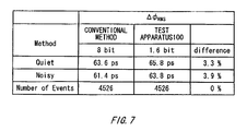
- FIG. 7 is a table showing jitter values actually measured by the testing apparatus as compared to jitter values actually measured by a conventional jitter measuring method.
- FIGS. 8A and 8B show exemplary configurations of a band limiting section.
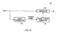
- FIG. 12 is a diagram showing another exemplary configuration of the measuring apparatus.
- FIG. 19 is a diagram showing a strobe signal generated by the strobe timing generator 30 .
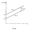
- FIG. 28 shows an example of instantaneous linear phase ⁇ J (t) and ⁇ K (t) of a signal-under-test J and a signal-under-test K;
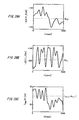
- FIG. 38 shows an example of series of comparison results obtained by the processing described in FIG. 37 :
- FIG. 38A shows an example of data series of the signal-under-test; and
- FIG. 38B shows an example of series of comparison results;
- FIG. 42 is an example of the spectrum of the signal-under-test measured by using the measuring apparatus 10 for the bit error rate
- the strobe timing generator 30 sequentially generates strobes at substantially even time intervals.
- the strobe timing generator 30 may sequentially generates strobes in synchronism with the period of the signal-under-test.
- the capture memory 40 stores a comparison result outputted from the comparator 20 .
- the capture memory 40 aligns and stores the comparison results sequentially outputted from the comparator 20 with respect to the associated strobe phase.
- the digital signal processing section 60 calculates jitter in the signal-under-test based on the comparison result stored in the capture memory 40 .
- the digital signal processing section 60 may calculate jitter in the signal-under-test by a method described later with reference to FIG. 5A and FIG. 5B . Additionally, the digital signal processing section 60 may calculate jitter in the signal-under-test by the other known technique.
- the data according to a signal processing method of the digital signal processing section 60 is inputted to the digital signal processing section 60 .
- the digital signal processing section 60 calculates jitter in the signal-under-test based on such as the zero crossing point of the signal-under-test, it is preferred that a signal indicative of a discrete value whose magnitude presents a discrete value in a range smaller than n (where, n is a real number).
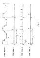
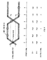
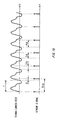
- FIG. 2 sows an example of strobe generated by a strobe timing generator 30 .
- the period of the signal-under-test is referred as T in the present embodiment.
- the strobe timing generator 30 sequentially generates strobes at substantially even time intervals in synchronism with or asynchronism with the period T of the signal-under-test.
- the testing apparatus 100 operates for each period (T 0 , T 1 , T 2 . . . ) corresponding to the operating period (test rate) in synchronism with the period T of the signal-under-test.
- the strobe timing generator 30 may generate a single strobe or plurality of strobes for each cycle in accordance with each test rate as shown in (1) and (2) of FIG. 2 . Additionally, the strobe timing generator 30 may generate strobes in asynchronism with the test rate as shown in (3) of FIG. 2 . At this time, the number of strobes generated for each cycle is defined based on the period for which the strobe timing generator 30 generates a strobe and the test rate. For example, the strobe timing generator 30 may be an oscillator circuit that operates independent of the operating period of the testing apparatus 100 .
- the period T of the signal-under-test may be corresponding to the test rate of the testing apparatus 100 or may not be corresponding to that. Additionally, when the testing apparatus 100 performs a functional test described later, it is preferred that the period T of the signal-under-test is corresponding to the test rate.
- the digital signal convert section 50 converts each of the comparison results (High, High), (Low, High) and (Low, Low) to digital values 1, 0 and ⁇ 1, respectively.
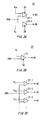
- the comparator 20 shown in FIG. 3B outputs different comparison results depending on whether or not the voltage value of the signal-under-test is greater than a threshold voltage value VT fed thereto. That is, the comparator 20 according to the present embodiment outputs the result by comparing two values.
- the comparator 20 includes a comparator 22 to which a threshold voltage value VT and the signal-under-test are inputted.
- the comparator 22 compares the voltage value of the signal-under-test with the threshold voltage value VT in response to a strobe provided from the strobe timing generator 30 . For example, when the voltage value of the signal-under-test is more than the threshold voltage value VT, the comparator 22 outputs the logical value indicative of High level. Meanwhile, when the voltage value of the signal-under-test is less than the threshold voltage value VT, the comparator 22 outputs the logical value indicative of Low level.
- the comparator 20 outputs the logical value outputted by the comparator 22 as a comparison result.
- the instantaneous phase estimating section 66 generates an instantaneous phase signal indicative of the instantaneous phase of a digital signal.
- the instantaneous phase of the digital signal can be derived form the inverse tangent (arctangent) of the ratio between the real part and the imaginary part of the analytic signal.
- FIG. 9 shows an example of frequency band passing through a filter 74 .
- the filter 74 passes therethrough the band without the carrier frequency among the frequency component of the signal-under-test.
- the carrier frequency component of the signal-under-test is not noise component and has energy larger than that of the other frequency component. Therefore, when the component of the carrier frequency is not removed, it will be required for the apparatus to provide a measuring range and an arithmetic operation range in which the energy of the carrier frequency may be dominant even though it is an unnecessary component in the measurement of noise. Therefore, it is unable to maintain sufficient resolution in the arithmetic operation and others for noise components that have very small energy as compared to the components of the carrier frequency and hence it is unable to accurately measure the noise component.
- the measuring apparatus 10 removes the carrier frequency component of the signal-under-test and extracts the noise component to be measured, so that the noise component can be accurately measured. Moreover, it is preferred that the filter 74 also removes the high frequency component of the carrier frequency component.
- the filter 75 receives a signal-under-test outputted by the device under test 200 , passes therethough an appropriate frequency components to be measured and inputs the same to the comparator 20 .
- the strobe timing generator 30 may sequentially generate further more strobes in another embodiment. By sequentially changing the offsets of those strobes, the an equivalent time measurement can be performed with high frequency.
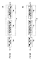
- FIG. 12 shows another example of the measuring apparatus 10 .
- the measuring apparatus 10 according to the present embodiment further includes a clock regenerator 25 in addition to the components of the measuring apparatus 10 described with reference to FIG. 1 .
- the other components are the same as those of the measuring apparatus 10 described with reference to FIG. 1-FIG . 11 , so that the description is omitted.
- the clock regenerator 25 generates a recovered clock in synchronism with a signal-under-test based on the signal-under-test and inputs the recovered clock to the strobe timing generator 30 as a trigger signal.
- the timing at starting to generate the strobe A and the strobe B described in FIG. 11 can be controlled, so that the strobe A and the strobe B having a predetermined phase difference therebetween can be generated.
- the measuring apparatus 10 may further more comparators 20 in another embodiment.
- a measurement with higher frequency can be performed by changing the offset of the strobe inputted to each comparator 20 .
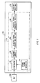
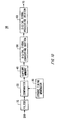
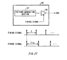
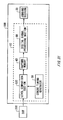
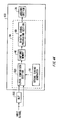
- the testing apparatus 100 further include a pattern generator 65 and a pattern comparison section 55 in addition to the components of the testing apparatus 100 described with reference to FIG. 1-FIG . 16 .
- the judging section 70 includes a logic judging section 75 and a jitter judging section 77 .
- Each of the other components has the function and the configuration of the components with the reference numerals the same as those of the components described with reference to FIG. 1-FIG . 16 .
- the strobe timing generator 30 generates a strobe.
- the strobe timing generator 30 When the functional test is performed, the strobe timing generator 30 generates the strobe in accordance with a test rate synchronized with the period of the signal-under-test. For example, the strobe timing generator 30 generates one strobe signal at almost-center timing of each test rate. Thereby the comparator 20 detects the logic level for each period of the signal-under-test.
- the pattern comparator 55 compares whether the logic level of the signal-under-test given by the comparison result stored in the capture memory 40 is coincident with a predetermined expected value pattern.
- the expected value pattern may be generated by the pattern generator 65 based on the logic level pattern of the test signal.
- the logic judging section 75 judges the pass/fail result for the device under test 200 based on the comparison result by the pattern comparison section 55 .
- the measuring apparatus 10 may have the same configuration as that of the measuring apparatus 10 described with reference to FIG. 1-FIG . 16 . Additionally, the measuring apparatus 10 may have the same configuration as that of the measuring apparatus 10 which will be described with reference to FIG. 19-FIG . 45 .
- the measuring apparatus 10 may include the comparator(s) 20 and the capture memory 40 . In this case, the comparators(s) 20 receive(s) strobes described with reference to FIG. 1-FIG . 16 .
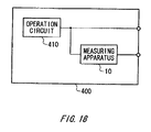
- the strobe may be provided from the outside, and also may be generated within the electronic device 400 .
- the phase of the strobe signal relative to that of the signal-under-test is changed by 5 ps for each period.
- the waveform is substantially the same for each period of the signal-under-test, so that the signal-under-test can be equivalently sampled at the period 5 ps.
- the digital signal converting section 50 may retrieve the comparison results with the total number of samples, which is determined by satisfying the restriction of corresponding to the integer number of cycles of the signal-under-test. That is, the digital signal converting section 50 may obtain the division result by calculating (the period of the signal-under-test)/(the difference between the period of the strobe and the period of the signal-under-test), and retrieve data with the integer multiple of the division result from the comparison results being continuously stored in the capture memory 40 .
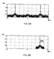
- FIG. 20B shows an example of extracted frequency component
- FIG. 20B shows an example of frequency component extracted when the carrier frequency of the signal-under-test is about 16 MHz, and the cutoff frequency is about 15 MHz+ ⁇ 5 MHz.
- the digital signal processing section 60 performs inverse Fourier Transform on the extracted frequency components to convert the same to a signal in the time domain.
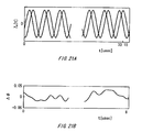
- FIG. 21A shows an example of signal in the time domain.
- the digital signal processing section 60 calculates the instantaneous phase ⁇ (t) of the signal-under-test based on the analytic signal. Additionally, the digital signal processing section 60 calculates the instantaneous phase noise ⁇ (t) of the signal-under-test by removing the linear component from the instantaneous phase.
- the method of calculating the instantaneous phase noise ⁇ (t) from the instantaneous phase ⁇ (t) is the same as the method shown in FIG. 6A .
- FIG. 21B shows an example of calculated instantaneous phase noise ⁇ (t).
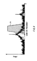
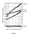
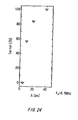
- FIG. 23 is a diagram illustrating the measurement band width dependency of the jitter value calculated for the cycle resolution ( ⁇ ).
- the jitter value according to the present embodiment is calculated for each cycle resolution ( ⁇ ) when the rms value of the jitter variation included in the signal-under-test is 2 ps.
- the horizontal axis in FIG. 23 is corresponding to the cutoff frequency shown in FIG. 23 .
- the cycle resolution ( ⁇ ) may be defined based on the standard deviation of the probability density function of jitter in the signal-under-test.
- the cycle resolution ( ⁇ ) i.e. an equivalent sampling interval based on the standard deviation will be described.
- ⁇ indicates the standard deviation of the probability density function of the jitter in the signal-under-test.
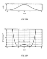
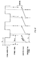
- FIG. 26 shows a relationship between the cycle resolution ( ⁇ ) and the measurement error.
- the horizontal axis indicates the cycle resolution ( ⁇ ) normalized by 2 ⁇ in FIG. 26 .
- the vertical axis indicates the measurement error corresponding to the above-described bias error. Additionally, measurements are performed four times as shown by circles and squares, and the measurement results are approximated by a curved line in the present embodiment.
- the strobe timing generator 30 of the measuring apparatus 10 may set or select the period of the strobes based on the standard deviation of the probability density function of jitter in the signal-under-test. For example, the strobe timing generator 30 may set the period of the strobes such that the standard deviation ⁇ of the jitter to be measured and the period of the signal-under-test are previously provided and the cycle resolution ( ⁇ ) is substantially equal to twice as large as the standard deviation ⁇ . The strobe timing generator 30 may set the period of the strobes such that the measurement error due to bias component is fallen within allowance. In this case, it is preferred that the strobe timing generator 30 sets the period of the strobes such that the cycle resolution ( ⁇ ) is around twice as large as the standard deviation ⁇ .
- the strobe timing generator 30 may select the timing set in which the cycle resolution ⁇ of the period is minimum among the timing sets, and also may select the timing set in which the cycle resolution ⁇ of the period is less than the value twice as large as the jitter value to be measured.
- the testing apparatus 100 when the testing apparatus 100 measures the deterministic skew or the random skew described in FIG. 28 and FIG. 29 , it is preferred that the testing apparatus 100 has two comparators 20 at the same time. Additionally, the same strobes are provided to the comparators 20 . That is, the testing apparatus 100 under-samples two signal-under-tests inputted to the comparators 20 at a time.
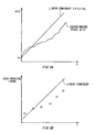
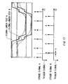
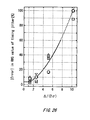
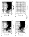
- FIG. 30 shows a comparison between a jitter measurement result by the testing apparatus 100 and a jitter measurement result by using a signal source analyzer E5052A.
- the range of the result of jitter measurement by using the signal source analyzer is indicated by dotted lines in FIG. 30 .
- the signal source analyzer may be a general measuring apparatus having a function to measure jitter.
- the strobe timing generator 30 sequentially generates strobes which are arranged at substantially even time intervals and each of which interval is larger than a bit time interval of the level of the signal-under-test is changed. Additionally, the signal-under test may be a signal of which signal level is alternatively changed to/from H level/L level for each bit time interval.
- the level comparison section 520 detects the signal level of the signal-under-test at a timing at which each strobe is sequentially provided.
- the level comparison section 520 may detect the signal level of the signal-under-test by using the comparator 20 described with reference to FIG. 1 .
- the voltage comparator 520 may sequentially compare the voltage value of the signal-under-test and the given threshold voltage value at a timing at which each strobe is sequentially provided. For example, the level comparison section 520 may output logical value 1 when the voltage value of the signal-under-test is greater than the threshold voltage value, and output a logical value ⁇ 1 when the comparison section 520 may compare a plurality of threshold voltage value different from each other with the voltage value of the signal-under-test. In this case, the level comparison section 520 outputs plural kinds of logical values corresponding to plural kinds of comparison results.
- the strobe timing generator 30 sequentially generates strobes at a period (T+ ⁇ ) different from the test rate (T) of the signal-under-test by a predetermined value ( ⁇ ). Moreover, the strobe timing generator 30 may output strobes for the signal-under-test for a period which does not satisfy Nyquist sampling theorem. For example, when the logical value of the signal-under-test is changed alternatively to H level or L level for each bit time interval, Nyquist sampling theorem is satisfied provided that the period of the strobe is less than the bit time interval (T). The strobe timing generator 30 may sequentially output strobes at a period slightly larger than the bit time interval. In this case, the level comparison section 520 detects H level and L level of the signal-under-test substantially in turn.
- the digital signal processing section holds the original value of 1 st , 3 rd , 5 th , 7 th 9 th . . . of data 60 among the data shown in FIG. 33A and FIG. 33B .
- the spectrum shown in FIG. 32C can be calculated by shifting the frequency components of the spectrum shown in FIG. 33B by ⁇ .
- the digital signal processing section 60 may calculate the spectrum of the signal-under-test (as shown in the right figure of FIG. 33C ) by shifting by ⁇ the frequency of the spectrum (the right figure of FIG. 33B ) obtained by Fourier-transforming the data series (the left figure of FIG. 33B ) which has not been processed to invert the data value. Further, the digital signal processing section 60 may calculate the waveform (as shown in the left figure of FIG. 33C ) of the signal-under-test by performing inverse Fourier transform on the such calculated spectrum of the signal-under-test.
- the inversion of the logical value may be a processing to convert the logic value H to the logic value L and convert the logic value L to the logic value H.
- the inversion of the data value may be a processing to invert the level of the signal-under-test, such as the voltage value on the basis of the intermediate level of the signal-under-test, such as zero voltage.
- FIG. 35 shows an example of configuration of the digital signal processing section 60 .
- the digital signal processing section 60 may perform at least a part of function of each component shown in FIG. 35 .
- the digital signal processing section 60 may be an electric computer.
- a program that causes the electronic computer to function as the digital signal processing section 60 described later in FIG. 35 is loaded onto the electronic computer.
- the jitter calculating section 632 calculates jitter in the signal-under-test based on the instantaneous phase noise calculated by the instantaneous phase noise calculating section 630 .
- the jitter calculating section 632 may calculate timing jitter for each edge of the signal-under-test by resampling the instantaneous phase noise at an edge timing of the signal-under-test.
- the edge timing of the signal-under-test may be a timing at which the waveform of the signal-under-test crosses the zero level.
- the jitter calculating section 632 may include a zero-crossing sampler that resamples the instantaneous phase noise.
- the jitter calculating section 632 may calculate periodic jitter in the signal-under-test based on the timing jitter and also may calculate peak-to-peak jitter in the signal-under-test.
- the analytic signal calculating section 626 calculates analytic signal z a (t) of the signal-under-test from the spectrum S a (f) of the signal-under-test in S 1006 .
- the analytic signal calculating section 626 obtains the analytic signal z a (t) as shown in FIG. 21A by extracting a predetermined frequency components of the spectrum Sa(f) of the signal-under-test z a (t) and perform the inverse Fourier transform on the same as shown in FIG. 20B .
- the instantaneous phase calculating section 628 obtains a continuous linear phase by removing the discontinuous phases from ARG(z a (t)) by means of a phase unwrapping by sequentially adding 2 ⁇ to the discontinuous phases ARG(z a (t)).
- the instantaneous phase noise calculating section 630 calculates instantaneous phase noise ⁇ (t) of the signal-under-test from instantaneous phase ⁇ (t) of the signal-under-test in S 1010 .
- the instantaneous phase noise calculating section 630 calculates the instantaneous phase noise ⁇ (t) by subtracting linear component 2 ⁇ f beat + ⁇ 0 from the instantaneous phase ⁇ (t) as described in FIG. 21B .
- the f beat is a frequency for equivalently sampling the signal-under-test with the cycle resolution ( ⁇ ).
- the f beat may be indicated by the following expression.
- the instantaneous phase noise calculating section 630 coverts the instantaneous phase noise ⁇ (t) in radian unit to the instantaneous phase noise ⁇ (t) in time unit in S 1012 .
- the instantaneous phase noise calculating section 630 may calculate the instantaneous phase noise ⁇ 100 (t) in time unit by dividing the instantaneous phase noise ⁇ (t) in radian unit by 2 ⁇ f 0 .
- f 0 is the average frequency of the signal-under-test calculated in S 1002 .
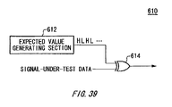
- FIG. 38 shows and example of series of comparison results obtained by the processing described in FIG. 37 .
- the measuring apparatus 10 alternately inverts the expected value (expected logical value) foe each bit time interval and compares the same with the logical value of the signal-under-test. For example, the measuring apparatus 10 inverts the expected values one by one.
- the waveform, the spectrum and the jitter of the signal-under-test described in FIG. 35 can be calculated based on the comparison result series shown in FIG. 38B . Additionally, the measuring apparatus 10 may calculate the comparison result series shown in FIG. 38B . Additionally, the measuring apparatus 10 may calculate the comparison result series not by inverting the expected value but by fixing the expected value to the logical value H. At this time, the comparison result series is equivalent to the data series shown in the left figure of FIG. 34B . As described above, the measuring apparatus 10 may calculate the spectrum of the signal-under-test by shifting by ⁇ the frequency of the spectrum obtained by performing the Fourier transform on the comparison result series. Additionally, the measuring apparatus 10 may calculate jitter in the signal-under-test based on the frequency components around any peak of the spectrum obtained by performing the Fourier-transform on the comparison result series.
- the code control section 610 may further include a test result memory that stores therein the comparison result outputted by the logical comparison section 614 .
- a circuit connected to the code control section 610 performs a signal processing based on the data series of the comparison result stored in the test result memory.
- the testing apparatus 100 may split the logical value outputted by the comparator 20 and provide the same to the capture memory 40 and the logical comparison section 614 .
- the output of the logical comparison section 614 is stored in the test result memory.
- the discrete signal converting section 50 and the digital signal processing section 60 process the data stored in either the capture memory 40 or the test result memory. For example, processing the data stored in the test result memory, the discrete signal converting section 50 and the digital signal processing section 60 may perform the processing as described with reference to FIG. 37-FIG . 43 .
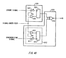
- FIG. 40 shows another configuration example of the level comparison section 520 and the code control section 610 .
- FIG. 41 is a timing chart showing an example of operation of the level comparison section 520 and the code control section shown in FIG. 40 .
- the expected value generating section 612 of the code control section 610 according to the present embodiment generates an expected value based on the signal-under-test.
- the measuring apparatus 10 may have a circuit that generates a synchronizing signal.
- the measuring apparatus 10 may have circuit that generate the synchronizing signal by using an oscillator circuit.
- the measuring apparatus 10 may have a circuit that generate the synchronizing signal based on the signal-under-test.
- the measuring apparatus 10 may have a clock recovering circuit that reproduce a clock synchronized with the signal-under-test by using such as a PLL circuit.
- the logical comparison section 614 may invert the input from the expected value generating section 612 and receive the same. Additionally, as shown in FIG. 40 , the exclusive OR of the output by the expected value generating section 612 and the output by the level comparison section 520 may be inverted and outputted.
- the state of the signal-under-test can be measured with a simple configuration.
- FIG. 42 is an example of the spectrum of the signal-under-test measured by using the measuring apparatus 10 for measuring the bit error rate.
- the horizontal axis of FIG. 42 indicates an offset frequency from the carrier frequency. That is, the spectrum of FIG. 42 indicates the spectrum of the jitter components.
- the measuring apparatus for measuring the bit error rate Even if the measuring apparatus for measuring the bit error rate is used, it can observe that jitter in the signal-under-test can be measured as shown in FIG. 42 .
- the period difference between the signal-under-test and the strobe is increased, the measurement resolution is increased, so that the measurement error is increased. If the period difference is octuple, and jitter is not detected in the present embodiment. Therefore, it is preferred that the period difference is more reduced.
- the expected value generating section 612 may generating an expected value fixed to a predetermined logical value. As shown in FIG. 43A , the expected value generating section 612 may generate the expected value fixed to the logical value H, for example. By such processing, the comparison result series can be obtained as shown in FIG. 43B .
- the digital signal processing section 60 may calculate the waveform, the spectrum and the jitter of the signal-under-test based on the comparison result series as described with reference to FIG. 35 .
- the voltage comparator 520 measures a signal inputted to the device under test 200 and a signal corresponding to the input signal outputted from the device under test 200 .
- the level comparison section 520 may measure the input signal and the output signal substantially at a time.
- the gain calculating section 634 calculates the jitter gain of the device under test 200 based on the jitter in the input signal and jitter in the output signal calculated by the jitter calculating section 632 , For example, the gain calculating section 634 may calculate the jitter gain of the device under test 200 based on the jitter ratio between the input signal and the output signal. Additionally, the gain calculating section 634 may calculate the jitter gain for each frequency component of sine wave jitter. In this case, the levels of the corresponding frequency components may be compared in the spectrum corresponding to jitter component for each of the input signal and the output signal calculated by the spectrum calculating section 624 .
- the analytic signal generating section 626 generates an analytic signal for each of the first signal-under-test and the second signal-under-test.
- the instantaneous phase calculating section 628 calculates the instantaneous phase for each of the first signal-under-test and the second signal-under-test.
- the above-described deterministic skew calculating section calculates the deterministic skew between the first signal-under-test and the second signal-under-test based on the instantaneous phase for each of the signal-under-test calculated by the instantaneous phase calculating section 628 .
- the digital signal processing section 60 may further include the random skew described with reference to FIG. 28 and FIG. 29 .
- the level comparison section 520 , the analytic signal generating section 626 and the instantaneous phase calculating 628 perform processing the same as the processing to calculate the above-described deterministic skew.
- the strobe timing generator 30 sequentially generates strobes which are arranged at substantially even time intervals and each of which interval is larger than the bit time interval.
- the strobe timing generator 30 may sequentially generates strobes which are arranged at substantially even time intervals and each of which interval is smaller than the bit time interval.
- the digital signal processing section 60 may generate a data series including data which are arranged at substantially even time intervals and each of which interval is larger than the bit time interval by removing the sampled data or the result by comparing with the expected value. Thereby the processing the same as that described in the embodiment can be performed.
- the jitter measurement of the device under test can be performed at low cost according to the present embodiment. Additionally, since the timing noise can be measured independent of the amplitude noise, the timing jitter can be accurately measured. Moreover, a measurement of jitter in a clock and data having the frequency higher than the maximum frequency of the strobe which can be generated by the strobe timing generator can be performed .
- a jitter test can be performed by using the hardware configuration of the current testing apparatus. That is, jitter can be measured by comparing the sample value with the expected value without pattern-matching.
Landscapes
- Engineering & Computer Science (AREA)
- General Engineering & Computer Science (AREA)
- Physics & Mathematics (AREA)
- General Physics & Mathematics (AREA)
- Tests Of Electronic Circuits (AREA)
Priority Applications (12)
| Application Number | Priority Date | Filing Date | Title |
|---|---|---|---|
| US11/623,101 US7856330B2 (en) | 2006-02-27 | 2007-01-15 | Measuring apparatus, testing apparatus, and electronic device |
| JP2008502777A JP4948522B2 (ja) | 2006-02-27 | 2007-02-26 | 測定装置、試験装置、及び電子デバイス |
| PCT/JP2007/053548 WO2007099918A1 (ja) | 2006-02-27 | 2007-02-26 | 測定装置、試験装置、及び電子デバイス |
| PCT/JP2007/053681 WO2007099970A1 (ja) | 2006-02-27 | 2007-02-27 | 測定装置、試験装置、電子デバイス、測定方法、プログラム、及び記録媒体 |
| TW096106844A TW200746708A (en) | 2006-02-27 | 2007-02-27 | Measuring device, testing device, electronic element, measuring method, program and record medium |
| PCT/JP2007/053682 WO2007099971A1 (ja) | 2006-02-27 | 2007-02-27 | 測定装置、試験装置、電子デバイス、プログラム、及び記録媒体 |
| JP2008502805A JP4948524B2 (ja) | 2006-02-27 | 2007-02-27 | 測定装置、試験装置、電子デバイス、プログラム、及び記録媒体 |
| JP2008502804A JP4948523B2 (ja) | 2006-02-27 | 2007-02-27 | 測定装置、試験装置、電子デバイス、測定方法、プログラム、及び記録媒体 |
| TW096106773A TW200739092A (en) | 2006-02-27 | 2007-02-27 | Measuring apparatus, testing apparatus, and electronic device |
| TW096106843A TW200739093A (en) | 2006-02-27 | 2007-02-27 | Measuring device, testing device, electronic element, program and record medium |
| US12/198,105 US8442788B2 (en) | 2006-02-27 | 2008-08-25 | Measuring device, test device, electronic device, measuring method, program, and recording medium |
| US12/198,096 US7970565B2 (en) | 2006-02-27 | 2008-08-25 | Measuring device, test device, electronic device, program, and recording medium |
Applications Claiming Priority (3)
| Application Number | Priority Date | Filing Date | Title |
|---|---|---|---|
| US11/362,536 US7398169B2 (en) | 2006-02-27 | 2006-02-27 | Measuring apparatus, measuring method, testing apparatus, testing method, and electronics device |
| US11/550,811 US7421355B2 (en) | 2006-02-27 | 2006-10-19 | Measuring apparatus, measuring method, testing apparatus, testing method, and electronic device |
| US11/623,101 US7856330B2 (en) | 2006-02-27 | 2007-01-15 | Measuring apparatus, testing apparatus, and electronic device |
Related Parent Applications (2)
| Application Number | Title | Priority Date | Filing Date |
|---|---|---|---|
| US11/362,536 Continuation-In-Part US7398169B2 (en) | 2006-02-27 | 2006-02-27 | Measuring apparatus, measuring method, testing apparatus, testing method, and electronics device |
| US11/550,811 Continuation-In-Part US7421355B2 (en) | 2006-02-27 | 2006-10-19 | Measuring apparatus, measuring method, testing apparatus, testing method, and electronic device |
Related Child Applications (2)
| Application Number | Title | Priority Date | Filing Date |
|---|---|---|---|
| PCT/JP2007/053681 Continuation-In-Part WO2007099970A1 (ja) | 2006-02-27 | 2007-02-27 | 測定装置、試験装置、電子デバイス、測定方法、プログラム、及び記録媒体 |
| PCT/JP2007/053682 Continuation-In-Part WO2007099971A1 (ja) | 2006-02-27 | 2007-02-27 | 測定装置、試験装置、電子デバイス、プログラム、及び記録媒体 |
Publications (2)
| Publication Number | Publication Date |
|---|---|
| US20080040060A1 US20080040060A1 (en) | 2008-02-14 |
| US7856330B2 true US7856330B2 (en) | 2010-12-21 |
Family
ID=38459024
Family Applications (1)
| Application Number | Title | Priority Date | Filing Date |
|---|---|---|---|
| US11/623,101 Expired - Fee Related US7856330B2 (en) | 2006-02-27 | 2007-01-15 | Measuring apparatus, testing apparatus, and electronic device |
Country Status (4)
| Country | Link |
|---|---|
| US (1) | US7856330B2 (ja) |
| JP (3) | JP4948522B2 (ja) |
| TW (3) | TW200739093A (ja) |
| WO (3) | WO2007099918A1 (ja) |
Cited By (6)
| Publication number | Priority date | Publication date | Assignee | Title |
|---|---|---|---|---|
| US20100153065A1 (en) * | 2007-09-11 | 2010-06-17 | Tokyo Electron Limited | Information processing device, information processing method and program |
| US20100275072A1 (en) * | 2009-04-24 | 2010-10-28 | Advantest Corporation | Correcting apparatus, pdf measurement apparatus, jitter measurement apparatus, jitter separation apparatus, electric device, correcting method, program, and recording medium |
| US20120001657A1 (en) * | 2010-06-30 | 2012-01-05 | Tektronix, Inc. | Apparatus and method for improved edge triggering in a test and measurement instrument |
| JP4948522B2 (ja) * | 2006-02-27 | 2012-06-06 | 株式会社アドバンテスト | 測定装置、試験装置、及び電子デバイス |
| US20140362895A1 (en) * | 2013-06-06 | 2014-12-11 | Hong Fu Jin Precision Industry (Shenzhen) Co., Ltd. | Method, program product, and test device for testing bit error rate of network module |
| US20170257107A1 (en) * | 2014-11-28 | 2017-09-07 | Advantest Corporation | Removal of sampling clock jitter induced in an output signal of an analog-to-digital converter |
Families Citing this family (18)
| Publication number | Priority date | Publication date | Assignee | Title |
|---|---|---|---|---|
| US7286947B1 (en) * | 2006-04-13 | 2007-10-23 | International Business Machines Corporation | Method and apparatus for determining jitter and pulse width from clock signal comparisons |
| US7945405B2 (en) * | 2008-05-08 | 2011-05-17 | Advantest Corporation | Jitter measurement apparatus, jitter measurement method, recording media, communication system and test apparatus |
| US7797121B2 (en) * | 2007-06-07 | 2010-09-14 | Advantest Corporation | Test apparatus, and device for calibration |
| JP5426821B2 (ja) * | 2007-09-05 | 2014-02-26 | オリンパス株式会社 | 内視鏡システム |
| US7808252B2 (en) * | 2007-12-13 | 2010-10-05 | Advantest Corporation | Measurement apparatus and measurement method |
| CN101932942B (zh) | 2008-02-05 | 2014-01-29 | 株式会社村田制作所 | 测定误差的修正方法及电子元器件特性测定装置 |
| US7933728B2 (en) * | 2008-05-08 | 2011-04-26 | Advantest Corporation | Skew measurement apparatus, skew measurement method, recording media and test apparatus |
| US8185336B2 (en) * | 2008-10-30 | 2012-05-22 | Advantest Corporation | Test apparatus, test method, program, and recording medium reducing the influence of variations |
| JPWO2010058441A1 (ja) * | 2008-11-19 | 2012-04-12 | 株式会社アドバンテスト | 試験装置、試験方法、および、プログラム |
| JP2010237214A (ja) * | 2009-03-30 | 2010-10-21 | Advantest Corp | ジッタ測定装置、ジッタ算出器、ジッタ測定方法、プログラム、記録媒体、通信システム、および試験装置 |
| JP5243340B2 (ja) * | 2009-05-08 | 2013-07-24 | 株式会社アドバンテスト | 試験装置および試験方法 |
| US8923894B1 (en) * | 2013-08-01 | 2014-12-30 | Tektronix, Inc. | Device for automated signal capture and location based on real-time analysis of signal characteristics |
| CN109884518A (zh) * | 2017-12-06 | 2019-06-14 | 爱德万测试公司 | 测试装置及测试方法 |
| US11047898B2 (en) * | 2019-02-12 | 2021-06-29 | Bae Systems Information And Electronic Systems Integration Inc. | Vector processing using amplitude or power detectors |
| CN111487447B (zh) * | 2020-05-09 | 2022-06-28 | 深圳市鼎阳科技股份有限公司 | 一种用于实现快速测量的数字示波器 |
| JP2022094048A (ja) * | 2020-12-14 | 2022-06-24 | 国立大学法人東海国立大学機構 | 信号較正装置、信号較正方法およびプログラム |
| JP7364616B2 (ja) * | 2021-04-14 | 2023-10-18 | アンリツ株式会社 | ジッタ耐力測定装置及びジッタ耐力測定方法 |
| CN113608109B (zh) * | 2021-08-10 | 2024-06-18 | 山东普赛通信科技股份有限公司 | 一种无线产品分时分频测试方法及系统 |
Citations (13)
| Publication number | Priority date | Publication date | Assignee | Title |
|---|---|---|---|---|
| US5260670A (en) | 1992-01-16 | 1993-11-09 | Tektronix, Inc. | Equivalent time sampler using an oscillator |
| JPH10288653A (ja) | 1997-04-15 | 1998-10-27 | Advantest Corp | ジッタ測定方法及び半導体試験装置 |
| WO2000046606A1 (fr) | 1999-02-08 | 2000-08-10 | Advantest Corporation | Dispositif et procede de mesure de gigue |
| JP2001289892A (ja) | 2000-01-31 | 2001-10-19 | Advantest Corp | ジッタ測定装置及びその方法 |
| DE10083886T1 (de) | 1999-11-19 | 2002-04-11 | Advantest Corp | Jittermessgerät und -verfahren sowie das Jittermessgerät aufweisendes Halbleiter-IC-Testgerät |
| US20030018442A1 (en) | 2001-04-03 | 2003-01-23 | Takahiro Yamaguchi | Apparatus for and method of measuring cross-correlation coefficient between signals |
| JP2003179142A (ja) | 2001-12-10 | 2003-06-27 | Nec Microsystems Ltd | ジッタ検査回路を搭載した半導体装置およびそのジッタ検査方法 |
| JP2004093345A (ja) | 2002-08-30 | 2004-03-25 | Renesas Technology Corp | ジッタ測定回路 |
| JP2004125552A (ja) | 2002-10-01 | 2004-04-22 | Advantest Corp | ジッタ測定装置、及び試験装置 |
| EP1508813A1 (en) | 2003-08-20 | 2005-02-23 | Agilent Technologies, Inc. | Spectral jitter analysis allowing jitter modulation waveform analysis |
| US20050149784A1 (en) | 2003-12-16 | 2005-07-07 | Masahiro Ishida | Testing apparatus and testing method |
| JP2005189093A (ja) | 2003-12-25 | 2005-07-14 | Advantest Corp | 試験装置 |
| US20050179576A1 (en) | 2004-02-12 | 2005-08-18 | Renesas Technology Corp. | Test circuit for evaluating characteristic of analog signal of device |
Family Cites Families (2)
| Publication number | Priority date | Publication date | Assignee | Title |
|---|---|---|---|---|
| US7856330B2 (en) * | 2006-02-27 | 2010-12-21 | Advantest Corporation | Measuring apparatus, testing apparatus, and electronic device |
| US7970565B2 (en) * | 2006-02-27 | 2011-06-28 | Advantest Corporation | Measuring device, test device, electronic device, program, and recording medium |
-
2007
- 2007-01-15 US US11/623,101 patent/US7856330B2/en not_active Expired - Fee Related
- 2007-02-26 WO PCT/JP2007/053548 patent/WO2007099918A1/ja active Application Filing
- 2007-02-26 JP JP2008502777A patent/JP4948522B2/ja not_active Expired - Fee Related
- 2007-02-27 WO PCT/JP2007/053682 patent/WO2007099971A1/ja active Application Filing
- 2007-02-27 JP JP2008502805A patent/JP4948524B2/ja not_active Expired - Fee Related
- 2007-02-27 WO PCT/JP2007/053681 patent/WO2007099970A1/ja active Application Filing
- 2007-02-27 TW TW096106843A patent/TW200739093A/zh unknown
- 2007-02-27 TW TW096106773A patent/TW200739092A/zh unknown
- 2007-02-27 JP JP2008502804A patent/JP4948523B2/ja not_active Expired - Fee Related
- 2007-02-27 TW TW096106844A patent/TW200746708A/zh unknown
Patent Citations (14)
| Publication number | Priority date | Publication date | Assignee | Title |
|---|---|---|---|---|
| US5260670A (en) | 1992-01-16 | 1993-11-09 | Tektronix, Inc. | Equivalent time sampler using an oscillator |
| JPH10288653A (ja) | 1997-04-15 | 1998-10-27 | Advantest Corp | ジッタ測定方法及び半導体試験装置 |
| WO2000046606A1 (fr) | 1999-02-08 | 2000-08-10 | Advantest Corporation | Dispositif et procede de mesure de gigue |
| DE10083886T1 (de) | 1999-11-19 | 2002-04-11 | Advantest Corp | Jittermessgerät und -verfahren sowie das Jittermessgerät aufweisendes Halbleiter-IC-Testgerät |
| JP2001289892A (ja) | 2000-01-31 | 2001-10-19 | Advantest Corp | ジッタ測定装置及びその方法 |
| US20030018442A1 (en) | 2001-04-03 | 2003-01-23 | Takahiro Yamaguchi | Apparatus for and method of measuring cross-correlation coefficient between signals |
| JP2003179142A (ja) | 2001-12-10 | 2003-06-27 | Nec Microsystems Ltd | ジッタ検査回路を搭載した半導体装置およびそのジッタ検査方法 |
| JP2004093345A (ja) | 2002-08-30 | 2004-03-25 | Renesas Technology Corp | ジッタ測定回路 |
| JP2004125552A (ja) | 2002-10-01 | 2004-04-22 | Advantest Corp | ジッタ測定装置、及び試験装置 |
| DE10393446T5 (de) | 2002-10-01 | 2005-09-08 | Advantest Corp. | Jittermessgerät und Testgerät |
| EP1508813A1 (en) | 2003-08-20 | 2005-02-23 | Agilent Technologies, Inc. | Spectral jitter analysis allowing jitter modulation waveform analysis |
| US20050149784A1 (en) | 2003-12-16 | 2005-07-07 | Masahiro Ishida | Testing apparatus and testing method |
| JP2005189093A (ja) | 2003-12-25 | 2005-07-14 | Advantest Corp | 試験装置 |
| US20050179576A1 (en) | 2004-02-12 | 2005-08-18 | Renesas Technology Corp. | Test circuit for evaluating characteristic of analog signal of device |
Non-Patent Citations (6)
| Title |
|---|
| Anderson, Christopher R. et al. "Performance Analysis of a Time-Interleaved Sampling Architecture for a Software Defined Ultra Wideband Receiver." Mobile and Portable Radio Research Group. Virginia Polytechnic Institute and State University. Proceeding of the SDR 05 Technical Conference and Product Exposition. Copyright © 2005 SDR Forum. 13 pages. |
| German Patent & Trademark Office. File No. 11 2007 000 506.8-35. Applicant Name: Advantest Corporation. Office Action dated Feb. 26, 2010. English Language Translation. 17 pages. |
| German Patent & Trademark Office. File No. 11 2007 000 506.8-35. Applicant Name: Advantest Corporation. Office Action dated Feb. 26, 2010. German Language. 13 pages. |
| German Patent & Trademark Office. File No. 11 2007 000 507.6-35. Applicant Name: Advantest Corporation. Office Action dated Mar. 3, 2010. English Language Translation. 15 pages. |
| German Patent & Trademark Office. File No. 11 2007 000 507.6-35. Applicant Name: Advantest Corporation. Office Action dated Mar. 3, 2010. German Language. 13 pages. |
| Jitter Measurements for CLK Generators or Synthesizers, Maxim Integrated Products, Sep. 26, 2003, pp. 1-4. |
Cited By (9)
| Publication number | Priority date | Publication date | Assignee | Title |
|---|---|---|---|---|
| JP4948522B2 (ja) * | 2006-02-27 | 2012-06-06 | 株式会社アドバンテスト | 測定装置、試験装置、及び電子デバイス |
| US20100153065A1 (en) * | 2007-09-11 | 2010-06-17 | Tokyo Electron Limited | Information processing device, information processing method and program |
| KR101150791B1 (ko) * | 2007-09-11 | 2012-06-13 | 도쿄엘렉트론가부시키가이샤 | 정보 처리 장치, 정보 처리 방법 및, 프로그램이 기록된 컴퓨터 판독가능 기록매체 |
| US20100275072A1 (en) * | 2009-04-24 | 2010-10-28 | Advantest Corporation | Correcting apparatus, pdf measurement apparatus, jitter measurement apparatus, jitter separation apparatus, electric device, correcting method, program, and recording medium |
| US8312327B2 (en) * | 2009-04-24 | 2012-11-13 | Advantest Corporation | Correcting apparatus, PDF measurement apparatus, jitter measurement apparatus, jitter separation apparatus, electric device, correcting method, program, and recording medium |
| US20120001657A1 (en) * | 2010-06-30 | 2012-01-05 | Tektronix, Inc. | Apparatus and method for improved edge triggering in a test and measurement instrument |
| US20140362895A1 (en) * | 2013-06-06 | 2014-12-11 | Hong Fu Jin Precision Industry (Shenzhen) Co., Ltd. | Method, program product, and test device for testing bit error rate of network module |
| US20170257107A1 (en) * | 2014-11-28 | 2017-09-07 | Advantest Corporation | Removal of sampling clock jitter induced in an output signal of an analog-to-digital converter |
| US9954546B2 (en) * | 2014-11-28 | 2018-04-24 | Advantest Corporation | Removal of sampling clock jitter induced in an output signal of an analog-to-digital converter |
Also Published As
| Publication number | Publication date |
|---|---|
| JPWO2007099971A1 (ja) | 2009-07-23 |
| WO2007099970A1 (ja) | 2007-09-07 |
| JPWO2007099918A1 (ja) | 2009-07-16 |
| TW200739093A (en) | 2007-10-16 |
| JP4948524B2 (ja) | 2012-06-06 |
| US20080040060A1 (en) | 2008-02-14 |
| WO2007099918A1 (ja) | 2007-09-07 |
| JP4948522B2 (ja) | 2012-06-06 |
| TW200746708A (en) | 2007-12-16 |
| JP4948523B2 (ja) | 2012-06-06 |
| TW200739092A (en) | 2007-10-16 |
| WO2007099971A1 (ja) | 2007-09-07 |
| JPWO2007099970A1 (ja) | 2009-07-23 |
Similar Documents
| Publication | Publication Date | Title |
|---|---|---|
| US7856330B2 (en) | Measuring apparatus, testing apparatus, and electronic device | |
| US7970565B2 (en) | Measuring device, test device, electronic device, program, and recording medium | |
| US7398169B2 (en) | Measuring apparatus, measuring method, testing apparatus, testing method, and electronics device | |
| JP5183520B2 (ja) | 測定装置および試験方法 | |
| US6990417B2 (en) | Jitter estimating apparatus and estimating method | |
| US7421355B2 (en) | Measuring apparatus, measuring method, testing apparatus, testing method, and electronic device | |
| US7636387B2 (en) | Measuring apparatus and measuring method | |
| US7317309B2 (en) | Wideband signal analyzing apparatus, wideband period jitter analyzing apparatus, and wideband skew analyzing apparatus | |
| US6922439B2 (en) | Apparatus for and method of measuring jitter | |
| US8442788B2 (en) | Measuring device, test device, electronic device, measuring method, program, and recording medium | |
| US7797121B2 (en) | Test apparatus, and device for calibration | |
| US20090048796A1 (en) | Test apparatus | |
| US7263150B2 (en) | Probability estimating apparatus and method for peak-to-peak clock skews | |
| US7206340B2 (en) | Characterizing jitter of repetitive patterns | |
| US6737852B2 (en) | Clock skew measuring apparatus and method | |
| US6775321B1 (en) | Apparatus for and method of measuring a jitter | |
| US8023558B2 (en) | Method and apparatus for measuring the input frequency response of a digital receiver | |
| US7638997B2 (en) | Phase measurement apparatus | |
| US20030219086A1 (en) | Jitter identification using a wide bandwidth oscilloscope |
Legal Events
| Date | Code | Title | Description |
|---|---|---|---|
| AS | Assignment |
Owner name: ADVANTEST CORPORATION, JAPAN Free format text: ASSIGNMENT OF ASSIGNORS INTEREST;ASSIGNORS:HOU, HARRY;YAMAGUCHI, TAKAHIRO;REEL/FRAME:019201/0518;SIGNING DATES FROM 20070124 TO 20070220 Owner name: ADVANTEST CORPORATION, JAPAN Free format text: ASSIGNMENT OF ASSIGNORS INTEREST;ASSIGNORS:HOU, HARRY;YAMAGUCHI, TAKAHIRO;SIGNING DATES FROM 20070124 TO 20070220;REEL/FRAME:019201/0518 |
|
| FEPP | Fee payment procedure |
Free format text: PAYOR NUMBER ASSIGNED (ORIGINAL EVENT CODE: ASPN); ENTITY STATUS OF PATENT OWNER: LARGE ENTITY |
|
| REMI | Maintenance fee reminder mailed | ||
| LAPS | Lapse for failure to pay maintenance fees | ||
| STCH | Information on status: patent discontinuation |
Free format text: PATENT EXPIRED DUE TO NONPAYMENT OF MAINTENANCE FEES UNDER 37 CFR 1.362 |
|
| FP | Lapsed due to failure to pay maintenance fee |
Effective date: 20141221 |