US7166889B2 - Semiconductor memory device having a gate electrode and a method of manufacturing thereof - Google Patents
Semiconductor memory device having a gate electrode and a method of manufacturing thereof Download PDFInfo
- Publication number
- US7166889B2 US7166889B2 US10/396,463 US39646303A US7166889B2 US 7166889 B2 US7166889 B2 US 7166889B2 US 39646303 A US39646303 A US 39646303A US 7166889 B2 US7166889 B2 US 7166889B2
- Authority
- US
- United States
- Prior art keywords
- layer
- oxide layer
- memory device
- semiconductor memory
- volatile semiconductor
- Prior art date
- Legal status (The legal status is an assumption and is not a legal conclusion. Google has not performed a legal analysis and makes no representation as to the accuracy of the status listed.)
- Expired - Fee Related
Links
Images


Classifications
-
- H—ELECTRICITY
- H10—SEMICONDUCTOR DEVICES; ELECTRIC SOLID-STATE DEVICES NOT OTHERWISE PROVIDED FOR
- H10B—ELECTRONIC MEMORY DEVICES
- H10B69/00—Erasable-and-programmable ROM [EPROM] devices not provided for in groups H10B41/00 - H10B63/00, e.g. ultraviolet erasable-and-programmable ROM [UVEPROM] devices
-
- H—ELECTRICITY
- H10—SEMICONDUCTOR DEVICES; ELECTRIC SOLID-STATE DEVICES NOT OTHERWISE PROVIDED FOR
- H10B—ELECTRONIC MEMORY DEVICES
- H10B41/00—Electrically erasable-and-programmable ROM [EEPROM] devices comprising floating gates
- H10B41/30—Electrically erasable-and-programmable ROM [EEPROM] devices comprising floating gates characterised by the memory core region
Definitions
- This present invention relates to a semiconductor memory device having a gate electrode and a method of manufacturing thereof, for example, a nonvolatile semiconductor memory device with a floating gate.
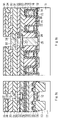
- FIG. 18 a shows a cross sectional view of a conventional nonvolatile semiconductor memory device.
- FIG. 18 b shows a cross sectional view of the conventional nonvolatile semiconductor memory device perpendicular direction to the FIG. 18 a .
- silicon oxide layers 123 , 128 , 131 , and 133 silicon oxide layers 123 , 128 , 131 , and 133 , a silicon nitride layer 134 , and a poly imide resin layer 135 is laminated above memory cells 200 .
- the memory cell 200 has first and second gate insulation layers 112 and 116 , a floating gate that comprises first and second poly crystalline silicon layers 114 and 115 , a control gate that comprises a third poly crystalline silicon layer 117 , a tungsten (W) silicide layer 118 , a silicon oxide layer 119 that is used as a mask layer, and diffusion layers 300 .
- a silicon nitride layer 121 is formed so as to cover the memory cells 200 .
- An insulation layer 122 is fulfilled among the memory cells 200 .
- FIGS. 19 to 24 show cross sectional views of manufacturing steps of the conventional nonvolatile semiconductor memory device. These FIGS. 19 to 24 are cross sectional views in same direction as the FIG. 18 b .
- FIGS. 19 to 24 are cross sectional views in same direction as the FIG. 18 b .
- memory cells are formed on a semiconductor substrate 111 .
- Element isolation layers 113 that have a STI (Shallow Trench Isolation) structure are formed in order to isolate among element regions (See FIG. 18 a ).
- a second silicon oxide layer 120 with a thickness of, for instance, 10 nm is formed on side surfaces of first to third poly crystalline silicon layers 114 , 115 , and 117 , a second gate insulation film 116 , and a tungsten silicide layer 118 and on surface of a first gate insulation layer 112 by adding heat with, for instance, 800 degrees centigrade and nitrogen atmosphere followed by adding heat with oxidization atmosphere.
- Diffusion layers 300 which are used as source or drain regions are formed by using an ion implantation method.
- a first silicon nitride layer 121 with a thickness of, for instance, 40 nm is formed on the first and second silicon oxide layers 119 and 120 by using a CVD (Chemical Vapor Deposition).
- the memory cells 200 are covered with the first silicon nitride layer 121 .
- a first insulation film 122 a that comprises a BPSG (Boron Phosphorous Silicate Glass) layer with a thickness of, for instance, 300 nm is formed on the first silicon nitride layer 121 by using a CVD method. After that, Heat with, for instance, 850 degrees centigrade and nitrogen atmosphere is added, thereby making the first insulation film 122 a reflowed.
- BPSG Bipolar Phosphorous Silicate Glass
- a second insulation film 122 b with a thickness of, for instance, 300 nm is deposited on the first insulation film 122 a . And then, heat with, for instance, 850 degrees centigrade and nitrogen atmosphere is added, thereby making the second insulation film 122 b reflowed.
- the first and second insulation layer are called as a insulation layer 122 .
- the insulation film 122 is flattened by using a CMP (Chemical Mechanical Polish) method so that an upper surface of the first silicon nitride layer 121 that is used as a stopper layer, is exposed. And then, Heat with, for instance, 850 degrees centigrade, 15 minutes, and nitrogen atmosphere, is added, thereby making the insulation layer 122 reflowd. Sequentially, heat with, for instance, 950 degrees centigrade and nitrogen atmosphere is added. A third silicon oxide layer 123 with a thickness of, for instance, 350 nm is deposed on the first silicon nitride layer 121 and the insulation layer 122 by using a plasma CVD method.
- CMP Chemical Mechanical Polish
- a photo resist layer (not shown) is processed to a predetermined pattern by using a photolithography technique. Predetermined portions of the third silicon oxide layer 123 and the insulation layer 122 are removed by using the photo resist layer as a mask and a RIE (Reactive Ion Etching) method. Thereby a first contact hole 124 is formed. After that, the photo resist layer is removed.
- RIE Reactive Ion Etching
- Portions of the first silicon nitride layer 121 , the second silicon oxide layer 120 , and the first gate insulation layer 112 that are formed at a bottom portion of the contact hole 124 , are removed so as to expose an upper surface of the semiconductor substrate 111 by using the third silicon oxide layer 123 as a mask and a RIE method. And then, Formations on a side surface of the first contact hole 124 are removed.
- a fourth poly crystalline silicon layer 125 with, for instance, 300 nm in thickness is deposited in the first contact hole 124 and on the third silicon oxide layer 123 by using a low pressure CVD method. By using a CDE (Chemical Dry Etching) method, the fourth poly crystalline silicon layer 125 deposited on the third silicon oxide layer 123 , is removed.
- an upper portion of the fourth poly crystalline silicon layer 125 is removed so that an upper surface of the fourth poly crystalline silicon layer 125 is lower than that of the third silicon oxide layer 123 . And then, heat with, for instance, 950 degrees centigrade and nitrogen atmosphere is added.
- a photo resist layer (not shown) is formed and processed to a predetermined pattern.
- the third silicon oxide layer 123 , the insulation layer 122 , and the first silicon nitride layer 121 are removed by using the photo resist layer with the predetermined pattern and a RIE method, thereby forming a second contact hole (not shown) on the semiconductor substrate 111 and a third contact hole (not shown) on the second poly crystalline silicon layer 115 .
- the third silicon oxide layer 123 , the first silicon nitride layer 121 , the first silicon oxide layer 119 , and the tungsten silicide layer 118 are removed, thereby forming a fourth contact hole (not shown) on the third poly crystalline silicon layer 117 .
- the photo resist layer of the predetermined pattern is removed.
- a photo resist layer (not shown) is formed and processed to a predetermined pattern.
- the third silicon oxide layer 123 is removed by using the photo resist layer of the predetermined pattern and a RIE method. And then, the photo resist layer of the predetermined pattern is removed.
- Impurities are injected into desirable areas of the silicon substrate 111 by using an ion implantation method.
- the impurities injected into the silicon substrate 111 are activated with, for instance, 950 degrees centigrade and nitrogen atmosphere by using a RTA (Rapid Thermal Annealing) method.
- RTA Rapid Thermal Annealing
- heat is added with, for instance, 550 degrees centigrade, 90 minutes, and nitrogen atmosphere.
- a first tungsten layer 127 with a thickness, for instance, of 400 nm is deposited on the titanium layer 126 .
- the titanium layer 126 and the first tungsten layer 127 are flattened to such an extent that an upper surface of the third silicon oxide layer 123 is exposed.
- Heat is added with, for instance, 400 degrees centigrade, 30 minutes, and a mixture gas of hydrogen and nitrogen.
- a fourth silicon oxide layer 128 is deposited on the third silicon oxide layer 123 , the titanium layer 126 , the first tungsten layer 127 .
- a photo resist layer (not shown) is patterned.
- the fourth silicon oxide layer 128 is processed by using the patterned photo resist layer as a mask, thereby, exposing a part of an upper surface of the tungsten layer 127 .
- the pattern photo resist layer is removed.
- a barrier metal layer (not shown) is formed on the first tungsten layer 127 and the fourth silicon oxide layer 128 .
- a second tungsten layer 129 is deposited on the barrier metal layer.
- the barrier metal layer and the second tungsten layer 129 are flattened to such an extent to expose an upper surface of the fourth silicon oxide layer 128 .
- a laminated layer 130 that comprises a barrier metal layer/an Al—Cu layer/a barrier metal layer (hereinafter, called as a first metal layer) is deposited.
- a photo resist layer (not shown) is patterned.
- the first metal layer is processed. And then, the patterned photo resist layer is removed.
- a fifth silicon oxide layer 131 is deposited on the fourth silicon oxide layer 128 and the first metal layer 130 . And then, by using a CMP method, the fifth silicon oxide layer 131 is flattened.
- a photo resist layer (not shown) is formed and patterned by using a photo lithography method. After that, the fifth silicon oxide layer 131 is removed by using the patterned photo resist layer as a mask, thereby espousing a part of an upper surface of the first metal layer 130 . The patterned photo resist layer is removed.
- a laminated layer (hereinafter called as a second metal layer 132 ) comprising a barrier metal layer and the Al—Cu layer is deposited.
- a photo resist layer (not shown) is formed on the second layer 132 and patterned by using a photo lithography method. After that, the second metal layer 132 is removed by using a patterned photo resist layer as a mask.
- a sixth silicon oxide layer 133 is formed on the fifth silicon oxide layer 131 and the second metal layer 132 . And then, heat is added with, for instance, 400 degrees centigrade and a mixture gas of hydrogen and nitrogen.
- a second silicon nitride layer 134 is formed on the fifth silicon oxide layer 131 , a poly imide resin layer 135 is deposited on the second silicon nitride layer 134 .
- the poly imide resin layer 35 , the second silicon nitride layer 134 , and the sixth silicon oxide layer 133 are removed, thereby exposing a part of an upper surface of the second metal layer 132 .
- a data retention test that is performed after the repeat test of date reprogramming operation, an alteration of “0” data (a situation where minus charged electrons are stored in the floating gate) into “1” data occurs. Therefore, it is difficult that the guaranteed number of a reprogramming test is increased.
- the data retention test is defined as a test for evaluating quickly at a high temperature.
- a first aspect of the present invention is providing a non-volatile semiconductor memory device, comprising: a memory cell having a tunnel oxide layer formed on a semiconducor substrate, a floating gate formed on the tunnel oxide layer, a control gate to which voltage is supplied, a source diffusion layer and a drain diffusion layer, the souce and drain diffusion layers formed in the semiconductor substrate adjacent to the tunnel oxide layer; a contact layer connected to the drain diffusion layer; and a layer formed above the memory cell, the layer comprising at least one of: 1) a silicon oxide layer to which nitrogen are doped, 2) a silicon oxide layer to which aluminum are doped, 3) an aluminum oxide layer, 4) a silicon layer to which titanium are doped, 5) a silicon oxide layer to which two of nitrogen, aluminum, and titanium are doped, 6) a silicon oxide layer to which nitrogen, aluminum, and titanium are doped, 7) a titanium oxide layer, 8) a titanium and aluminum oxide layer, 9) a simple metal layer comprising one of Ti, Ni, Co, Zr, Cu, Pt,
- a second aspect of the present invention is providing a method of manufacturing a non-volatile semiconductor memory device, comprising: forming a source diffusion layer and a drain diffusion layer in a semiconductor substrate: forming a tunnel oxide layer on the semiconductor substrate adjacent to the source and the drain diffusion layers: forming a floating gate above the tunnel oxide layer; forming a control gate above the floating gate; and forming a layer formed above the memory cell, the layer comprising at least one of: 1) a silicon oxide layer to which nitrogen are doped, 2) a silicon oxide layer to which aluminum are doped, 3) an aluminum oxide layer, 4) a silicon oxide layer to which titanium are doped, 5) a silicon oxide layer to which two of nitrogen, aluminum, and titanium are doped, 6) a silicon oxide layer to which nitrogen, aluminum, and titanium are doped, 7) a titanium oxide layer, 8) a titanium and aluminum oxide layer, 9) a simple metal layer comprising one of Ti, Ni, Co, Zr, Cu, Pt, V, Mg, U, Nd, La,
- FIG. 1 a shows a cross sectional view of a non-volatile semiconductor memory device of a first embodiment in a present invention.
- FIG. 1 b shows a cross sectional view perpendicular to a non-volatile semiconductor memory device shown in FIG. 1 a.
- FIG. 2 shows a manufacturing step of a non-volatile semiconductor memory device associated with the first embodiment of the present invention.
- FIG. 3 shows a manufacturing step of a non-volatile semiconductor memory device associated with the first embodiment of the present invention followed by FIG. 2 .
- FIG. 4 shows a manufacturing step of a non-volatile semiconductor memory device associated with the first embodiment of the present invention followed by FIG. 3 .
- FIG. 5 shows a manufacturing step of a non-volatile semiconductor memory device associated with the first embodiment of the present invention followed by FIG. 4 .
- FIG. 6 shows a manufacturing step of a non-volatile semiconductor memory device associated with the first embodiment of the present invention followed by FIG. 5 .
- FIG. 7 shows a manufacturing step of a non-volatile semiconductor memory device associated with the first embodiment of the present invention followed by FIG. 6 .
- FIG. 8 shows a cross sectional view of a non-volatile semiconductor memory device of a second embodiment in a present invention.
- FIG. 8 b shows a cross sectional view perpendicular to a non-volatile semiconductor memory device shown in FIG. 8 a.
- FIG. 9 shows a manufacturing step of a non-volatile semiconductor memory device associated with the second embodiment of the present invention followed by FIG. 8 .
- FIG. 10 shows a manufacturing step of a non-volatile semiconductor memory device associated with the second embodiment of the present invention followed by FIG. 9 .
- FIG. 11 shows a manufacturing step of a non-volatile semiconductor memory device associated with the second embodiment of the present invention followed by FIG. 10 .
- FIG. 12 shows a manufacturing step of a non-volatile semiconductor memory device associated with the second embodiment of the present invention followed by FIG. 11 .
- FIG. 13 shows a cross sectional view of a non-volatile semiconductor memory device of a third embodiment in a present invention.
- FIG. 13 b shows a cross sectional view perpendicular to a non-volatile semiconductor memory device shown in FIG. 13 a.
- FIG. 14 shows a manufacturing step of a non-volatile semiconductor memory device associated with the third embodiment of the present invention followed by FIG. 13 .
- FIG. 15 shows a manufacturing step of a non-volatile semiconductor memory device associated with the third embodiment of the present invention followed by FIG. 14 .
- FIG. 16 shows a cross sectional view of a non-volatile semiconductor memory device of a fourth embodiment in a present invention.
- FIG. 16 b shows a cross sectional view perpendicular to a non-volatile semiconductor memory device shown in FIG. 16 a.
- FIG. 17 shows a manufacturing step of a non-volatile semiconductor memory device associated with the fourth embodiment of the present invention followed by FIG. 16 .
- FIG. 18 a shows a cross sectional view of a conventional non-volatile semiconductor memory device.
- FIG. 18 b shows a cross sectional view perpendicular to a non-volatile semiconductor memory device shown in FIG. 18 a.
- FIG. 19 shows a manufacturing step of the conventional non-volatile semiconductor memory device.
- FIG. 20 shows a manufacturing step of a conventional non-volatile semiconductor device followed by FIG. 19 .
- FIG. 21 shows a manufacturing step of a conventional non-volatile semiconductor device followed by FIG. 20 .
- FIG. 22 shows a manufacturing step of a conventional non-volatile semiconductor device followed by FIG. 21 .
- FIG. 23 shows a manufacturing step of a conventional non-volatile semiconductor device followed by FIG. 22 .
- FIG. 24 shows a manufacturing step of a conventional non-volatile semiconductor device followed by FIG. 23 .
- FIG. 25 shows a diagram of a memory card in which a semiconductor memory device is arranged.
- FIG. 26 shows a diagram of a memory card in which a semiconductor memory device and a controller are arranged.
- FIG. 27 shows a diagram of a card holder to which a memory card is inserted.
- FIG. 28 shows a diagram of a connecting apparatus, a board, and a connecting wire.
- FIG. 29 shows a diagram of a PC, a connecting apparatus, and a connecting wire.
- FIG. 30 shows a diagram of an IC chip including a semiconductor memory device, and an IC card on which the IC card is allocated.
- FIG. 31 shows a schematic diagram of an IC card and an IC chip.
- a layer to capture the hydrogen or to prevent the hydrogen from diffusing is formed above a non-volatile semiconductor memory device in order to upgrade the data retention characteristic.
- the layer to capture the hydrogen or prevent the hydrogen from diffusing is Al 2 O 3 (Aluminum oxide) layer.
- the Al 2 O 3 (Aluminum oxide) layer is formed above the non-volatile semiconductor memory device.
- FIG. 1 a shows a cross sectional view of the non-volatile semiconductor memory device of the first embodiment in the present invention.
- FIG. 1 b shows a perpendicular cross sectional view of the FIG. 1 a .
- a structure and a manufacturing method of the first embodiment in the present invention will be explained.
- the non-volatile semiconductor memory device of the present invention has an Al 2 O 3 (Aluminum oxide) layer 10 to capture the hydrogen or to prevent the hydrogen from diffusing above the non-volatile semiconductor memory device.
- the Al 2 O 3 (Aluminum oxide) layer 10 is formed between the non-volatile semiconductor memory device and a second metal layer 32 .
- the non-volatile semiconductor memory device has first and second gate insulating films 12 and 16 , a floating gate of first and second polycrystalline silicon layers 14 and 15 , a control gate of a third polycrystalline silicon layer 17 , a tungsten (W) silicide layer 18 , and a first silicon oxide 19 used as a mask layer of a gate electrode that comprises the floating gate, the control gate, and the tungsten (W) silicide layer 18 .
- a first silicon oxide layer 21 is formed to cover the non-volatile semiconductor memory device.
- An insulating film 22 is buried among the non-volatile semiconductor memory devices.
- the Al 2 O 3 layer 10 is formed on a silicon nitride layer 21 that is formed on the first silicon oxide 19 , and the insulating layer 22 that is buried among the non-volatile semiconductor memory devices.
- FIGS. 2 through 15 show cross sectional views in which a manufacturing method of the non-volatile semiconductor memory device of the first embodiment in the present invention is depicted.
- the FIGS. 2 through 15 show cross sectional views in same direction as FIG. 1 b .
- the manufacturing method of the non-volatile semiconductor memory device of the first embodiment in the present invention will be explained.
- a gate insulation film 12 is formed on a semiconductor substrate 11 .
- the gate electrodes 500 are formed on the gate insulation film 12 .
- each of the gate electrode 500 is comprised of the floating gate of the first and second polycrystalline silicon layers 14 and 15 , the second gate insulation film 16 , the control gate of the third polycrystalline silicon layer 17 , and the tungsten (W) silicide layer 18 .
- the first silicon oxide 19 is formed on the tungsten (W) silicide layer 18 .
- element isolation insulation layers 13 each of which has a STI (Shallow Trench Isolation) structure are formed ( FIG. 1 a ).
- heat is added with, for instance, 800 degrees centigrade and nitrogen atmosphere.
- heat is add with oxide atmosphere, thereby forming a second silicon oxide layer 20 with, for instance, a thickness of 10 nm on surfaces of the first to third poly crystalline silicon layer 14 , 15 , and 17 , the second gate insulation film 16 , and the tungsten silicide layer 18 , and on upper surface of the first gate insulation layer 12 .
- impurities are implanted to areas of source and drain regions 52 .
- a silicon nitride layer 21 with, for instance, a thickness of 40 nm is formed on the first and second silicon layer 19 and 20 . Thereby, the non-volatile semiconductor memory devices are covered with the first silicon nitride layer 21 . And then, by using a CVD method, a first insulation layer 22 a of a BPSG (Boron Phosphorous Silicon Glass) layer with, for instance, a thickness of 300 nm is formed on the first silicon nitride layer 21 . After that, heat is added with, for instance, 850 degrees centigrade and nitrogen atmosphere. Thereby, the insulation film 22 a is reflowed.
- BPSG Bipolar Phosphorous Silicon Glass
- a second insulation film 22 b with, for instance, 850 degrees centigrade and nitrogen atmosphere is formed on the first insulation film 22 a . After that, heat is added with, for instance, 850 degrees centigrade and nitrogen atmosphere. Thereby, the second insulation layer 22 b is reflowed.
- the first and second insulation layer 22 a and 22 b are referred as a insulation layer 22 .
- the insulation layer 22 is flattened to such an extent that an upper surface of the first silicon nitride layer 21 that is used as a stopper layer is exposed. After that, heat is added with, for instance, 850 degrees centigrade, 15 minutes, and nitrogen atmosphere. Thereby, the insulation layer 22 is reflowed. Sequentially, heat is added with, for instance, 950 degrees centigrade and nitrogen atmosphere.
- a PVD Physical Vapor Deposition
- the Al 2 O 3 (Aluminum oxide) layer 10 with, for instance, a thickness of 10 nm is formed on the insulation layer 22 .
- a third silicon oxide layer 23 with, for instance, a thickness of 350 nm is formed on the Al 2 O 3 layer 10 by using a plasma CVD method.
- a resist layer (not shown) is processed into a predetermined pattern by using a photo lithography technique, predetermined portions of the third silicon oxide layer 23 , the Al 2 O 3 layer 10 , and the insulation layer 22 are removed to form a first contact hole 24 by using the patterned resist layer as a mask, and a RIE (Reactive Ion Etching) method. After that, the patterned resist layer is removed.
- the first silicon nitride layer 21 , the second silicon oxide layer 20 , and the first gate insulation film 12 which are formed on a bottom portion of the first contact hole 24 , are removed so as to expose an upper surface of the semiconductor substrate 11 by using a RIE method and the third silicon oxide layer 23 as a mask. After that, formation that is formed on a side surface of the first contact hole 24 is removed.
- a fourth poly crystalline silicon layer 25 with, for instance, a thickness of 300 nm is formed in the first contact hole 24 and on the third silicon oxide layer 23 .
- CDE Chemical Dry Etching
- an upper portion of the fourth poly crystalline silicon layer 25 is removed so that an upper surface of the fourth poly crystalline silicon layer 25 is lower than that of the third silicon oxide layer 25 .
- heat is added with, for instance, 950 degrees centigrade and nitrogen atmosphere.
- a resist layer (not shown) is formed and patterned with a predetermined pattern. And then, by using a RIE method and the patterned resist layer as a mask, the third silicon oxide layer 23 , the insulation layer 22 , and the first silicon nitride layer 21 are removed, thereby forming a second contact hole (not shown), which reaches the upper surface of the semiconductor substrate 11 . At same time, the third silicon oxide layer 23 , the insulation layer 22 , and the first silicon nitride layer 21 are removed, thereby forming a third contact hole (not shown), which reaches the upper surface of the second poly crystalline silicon layer 15 .
- the third silicon oxide layer 23 , the first silicon nitride layer 21 , the first silicon oxide layer 19 , and the tungsten silicide layer 18 are removed, thereby forming a fourth contact hole (not shown), which reaches the upper surface of the third poly crystalline silicon layer 15 .
- a resist layer (not shown) is formed and patterned with a predetermined pattern. And then, by using a RIE method and the patterned resist layer as a mask, the third silicon oxide layer 23 is removed. After that, the patterned resist layer is removed. Impurities are injected into a desirable area by using an ion implantation method. And then, heat is added by using a RTA (Rapid Thermal Annealing) method with, for instance, 950 degrees centigrade and nitrogen atmosphere, thereby activating the impurities injected.
- RTA Rapid Thermal Annealing
- a Ti (titanium) layer 26 with, for instance, a thickness of 30 nm is formed.
- Heat is added with, for instance, 550 degrees centigrade, 90 minutes, and nitrogen atmosphere containing hydrogen.
- a first W (tungsten) layer 27 with, for instance, a thickness of 400 nm is formed on the Ti layer 26 by using a PVD method.
- the Ti layer 26 and the first W layer 27 is flattened to such an extent that an upper surface of the third silicon oxide layer 23 is exposed by using a CMP method.
- heat is added with, for instance, 400 degrees centigrade, 30 minutes, and a mixture gas of hydrogen and nitrogen.
- a fourth silicon oxide layer 28 is formed on the third silicon oxide layer 23 , the Ti layer 26 , and the first W layer 27 .
- a resist layer (not shown) is formed and patterned.
- the fourth silicon oxide layer 28 is removed by using the patterned resist layer as a mask, thereby exposing a portion of an upper surface of the first W layer 27 .
- the resist layer patterned is removed.
- a barrier metal (not shown) is formed on the first W layer 27 and the fourth silicon oxide layer 28 .
- a second W layer 29 is formed on the barrier metal. After that, by using a CMP method, the barrier metal and the second W layer 29 are flattened to such an extent that an upper surface of the fourth silicon oxide layer 28 is exposed.
- a fifth silicon oxide layer 31 is formed on the fourth silicon oxide layer 28 and the first metal layer 30 .
- the fifth silicon oxide layer 31 is flattened.
- a resist layer (not shown) is formed and patterned.
- the fifth silicon oxide layer 31 is processed, thereby exposing a portion of an upper surface of the first metal layer 30 .
- the resist layer patterned is removed.
- a laminated layer 32 that is comprised of a barrier metal layer/an Al—Cu layer (hereinafter, referred as a second metal layer), is formed.
- a resist layer (not shown) is formed and patterned.
- the second metal layer 32 is processed. After that, the resist layer patterned is removed.
- a sixth silicon oxide layer 33 is formed on the fifth silicon oxide layer 31 and the second metal layer 32 .
- heat is added with, for instance, 400 degrees centigrade and a mixture gas of hydrogen and nitrogen.
- a second silicon nitride layer 34 is formed on the fifth silicon oxide layer 31 .
- a poly imide resin 35 is formed on the second silicon nitride layer 34 .
- portions of the poly imide resin 35 , the second silicon nitride layer 34 , and the sixth silicon oxide layer 33 are removed, thereby exposing a portion of an upper surface of the second metal layer 32 .
- a layer that is formed above the non-volatile semiconductor memory device would not be limited to the Al 2 O 3 layer 10 and may be a layer that prevents hydrogen from diffusing (containing a layer that captures hydrogen).
- the layer that prevents hydrogen from diffusing may be a layer as follows.
- a first example of the layer that prevents hydrogen from diffusing is a silicon oxide layer to which nitride are doped.
- the silicon oxide layer to which nitride are doped may be formed by injecting nitrogen atoms into a silicon oxide layer with, for instance, acceleration energy 25 KeV and dose quantity 1 ⁇ 10 15 cm ⁇ 2 .
- the silicon oxide layer to which nitride are doped may be formed by a CVD method that can use gas with nitrogen and without hydrogen, for instance, N 2 O or NF 3 etc.
- the silicon oxide layer to which nitride are doped may be formed by adding heat with, for instance, 800 degrees centigrade, ammonia (NH 3 ) atmosphere and 30 minutes.
- the silicon oxide layer to which nitride may be formed by a HDPCV method.
- a second example of the layer that prevents hydrogen from diffusing is a silicon oxide layer to which aluminum are doped.
- the silicon oxide layer to which aluminum are doped may be formed by injecting aluminum ions into a silicon oxide layer.
- the silicon oxide layer to which aluminum are doped may be formed by using a CVD method.
- the silicon oxide layer to which aluminum are doped may be formed by adding heat with oxygen atmosphere after forming an alloy of Al and Si.
- the silicon oxide layer to which aluminum are doped may be formed by using a PVD method.
- a third example of the layer that prevents hydrogen from diffusing is an aluminum oxide layer.
- the aluminum oxide layer may be formed by using a CVD or a PVD method. Also, the aluminum oxide layer may be formed by adding heat with oxygen atmosphere after aluminum was formed.
- a fourth example of the layer that prevents hydrogen from diffusing is a silicon oxide layer to which titanium are doped.
- the silicon oxide layer to which titanium are doped may be formed by injecting titanium ions into a silicon oxide layer. Also, the silicon oxide layer to which titanium are doped may be formed by using a CVD method.
- a fifth example of the layer that prevents hydrogen from diffusing is a silicon oxide layer to which two of nitrogen, aluminum, and titanium are doped.
- a sixth example of the layer that prevents hydrogen from diffusing is a silicon oxide layer to which nitrogen, aluminum, and titanium are doped.
- a seventh example of the layer that prevents hydrogen from diffusing is a titanium oxide layer.
- the titanium oxide layer may be formed by a PVD method.
- the titanium oxide layer may be formed by adding heat with oxygen atmosphere after forming a titanium layer.
- An eighth example of the layer that prevents hydrogen from diffusing is a titanium and aluminum oxide layer.
- a ninth example of the layer that prevents hydrogen from diffusing is a simple metal layer comprising one of Ti, Ni, Co, Zr, Cu, Pt, V, Mg, U, Nd, La, and Sc.
- the layer that prevents hydrogen from diffusing may be an alloy layer comprising at least two of Ti, Ni, Co, Zr, Cu, Pt, V, Mg, U, Nd, La, and Sc, and the at least two of Ti, Ni, Co, Zr, Cu, Pt, V, Mg, U, Nd, La, and Sc are included 50% or more.
- the layer that prevents hydrogen from diffusing may be a nitrogenous layer of the alloy layer.
- the layer that prevents hydrogen from diffusing may be a hydrogenated layer of the alloy layer.
- the layer that prevents hydrogen from diffusing is, for instance, TiNi, Ti—Co, Ti—Cu, Ni—Zr, Ti—Pt, or Zr—Cu etc.
- the Al 2 O 3 layer is formed above the memory cell, thereby preventing hydrogen from intruding into the memory cell.
- a data retention test after programming a data to the memory cell which is a test for measuring a time period in which data is stored in the memory cell programmed, results in 0.3 V or less of fluctuations in threshold voltage in the first embodiment as opposed to about 0.5 V of that in a conventional technique.
- the first embodiment of the present invention allows a characteristic of the data retention to make good.
- a silicon oxide layer to which nitrogen is doped can be used instead of the third silicon oxide layer 23 .
- the silicon oxide layer to which nitrogen are doped is formed by a CVD method at which SiH 4 , N 2 O, and N 2 are used.
- the silicon oxide layer to which nitrogen are doped can prevent furthermore hydrogen from intruding into the memory cell, thereby making an improvement of the data retention characteristic.
- a second embodiment of the present invention is different from the first embodiment of the present invention in that an Al 2 O 3 layer is formed on a silicon oxide layer that is formed above memory cells.
- FIG. 8 a shows a cross sectional view of a non-volatile semiconductor memory device of the second embodiment in the present invention.
- FIG. 8 b shows a cross sectional view perpendicular to the non-volatile semiconductor memory device shown in FIG. 8 a .
- the structure of the non-volatile semiconductor memory device of the second embodiment is different from that of the first embodiment in that a Al 2 O 3 layer 10 is formed on a third silicon oxide layer 23 that is formed above memory cells. Similarly to the first embodiment, the Al 2 O 3 layer 10 is formed between the memory cells and a second metal layer 32 .
- FIGS. 9 to 12 show cross sectional views of manufacturing the non-volatile semiconductor memory device of the second embodiment in the present invention. Hereinafter, a manufacturing step of the non-volatile semiconductor memory device of the second embodiment will be explained.
- the insulation film 22 is flattened, by using a CMP method, so as to expose an upper surface of the first silicon nitride layer 23 that is used as a stopper layer.
- the insulation film 22 is reflowed by adding heat with, for instance, 850 degrees centigrade, 15 minutes, and nitrogen atmosphere followed by adding heat with, for instance, 950 degrees centigrade and nitrogen atmosphere.
- a third silicon oxide layer 23 with, for instance, 350 nm in thickness is formed on the first silicon nitride layer 21 and the insulation film 22 .
- a resist layer (not shown) with a predetermined pattern is formed. Predetermined portions of the third silicon oxide layer 23 and the insulation film 22 are removed by using a RIE method and the patterned resist layer as a mask, thereby forming a first contact hole 24 . After that, the patterned resist layer is removed.
- a forth polycrystalline silicon layer 25 is formed in the first contact hole after the first silicon nitride layer 21 , the second silicon oxide layer 20 , and the first gate insulation film 12 that are formed on a bottom of the first contact hole 24 , are removed. After that, Second to fourth contact holes are formed (not shown).
- a Ti layer 26 and a first W layer 27 are formed after the third silicon oxide layer 23 is processed. And then, by using a CMP method, the Ti layer 26 and the first W layer 27 are flattened so as to expose an upper surface of the third silicon oxide layer 23 .
- an Al 2 O 3 layer 10 with, for instance, 10 nm in thickness is formed on the third silicon oxide 23 , the Ti layer 26 , and the first W layer 27 .
- a fourth silicon oxide layer 28 is formed on the Al 2 O 3 layer 10 . Portions of the fourth silicon oxide layer 28 and the Al 2 O 3 layer 10 are removed, thereby exposing a portion of an upper surface of the first W layer 27 .
- a second W layer 29 is formed on the first W layer 27 and the fourth silicon oxide layer 28 , and then, the second W layer is flattened.
- a first metal layer 30 is formed on the fourth silicon oxide layer 28 and the second W layer 29 . After that, the first metal layer 30 is processed.
- a fifth silicon oxide layer 31 is formed on the fourth silicon oxide layer 28 and the first metal layer 30 .
- the fifth silicon oxide layer 31 is flattened. And then, the fifth silicon oxide layer 31 is processed, thereby exposing a portion of an upper surface of the first metal layer 30 .
- the second metal layer 32 is formed and processed.
- a sixth silicon oxide layer 33 , a second silicon nitride layer 34 , and a poly imide resin layer 35 are formed. After that, the poly imide resin layer 35 , the second silicon nitride layer 34 , and the sixth silicon oxide layer 33 are processed, thereby exposing a portion of an upper surface of the second metal layer 32 .
- the second embodiment of the present invention has same effects as the first embodiment of the present invention.
- a silicon oxide layer in which nitrogen are doped could be allowed to use, instead of the fourth silicon oxide layer 28 .
- the silicon oxide layer in which nitrogen are doped could be formed by using a plasma CVD method with, for instance, SiH 4 , N 2 O, and N 2 .
- a third embodiment of the present invention is different from the first embodiment of the present invention in that an Al 2 O 3 layer is formed on a silicon oxide layer that is formed above an upper lines.
- FIG. 13 a shows a cross sectional view of a non-volatile semiconductor memory device of the third embodiment in the present invention.
- FIG. 13 b shows a cross sectional view perpendicular to the non-volatile semiconductor memory device shown in FIG. 13 a .
- a non-volatile semiconductor memory device of the third embodiment in the present invention is different from that of the first embodiment in the present invention in that an Al 2 O 3 layer 10 is formed on a sixth silicon oxide layer 33 that is formed on a second metal layer 32 . Therefore, we will omit an explanation about a structure of the non-volatile semiconductor memory device in the third embodiment, because the structure of the non-volatile semiconductor memory device in the third embodiment is same as that of the first embodiment.
- FIGS. 14 and 15 show cross sectional views of the manufacturing steps of the non-volatile semiconductor memory device of the third embodiment in the present invention.
- FIGS. 14 and 15 show cross sectional views of the manufacturing steps of the non-volatile semiconductor memory device of the third embodiment in the present invention.
- same manufacturing steps of the non-volatile semiconductor memory device in the third embodiment as that of the first embodiment would be omitted or simplified.
- a fourth silicon oxide layer 28 is formed on the third silicon oxide layer 23 , the Ti layer 26 , and the first W layer 27 .
- a predetermined portion of the fourth silicon oxide layer 28 is removed so as to expose a portion of an upper surface of the first W layer 27 .
- a second W layer 29 is formed on the first W layer 27 and the fourth silicon oxide layer 28 . And then, the second W layer 29 is flattened. After that, the first metal layer 30 is formed and processed.
- a fifth silicon oxide layer 31 is formed on the fourth silicon oxide layer 28 and the first metal layer 30 , and then, the fifth silicon oxide layer 31 is flattened. After that, a predetermined portion of the fifth silicon oxide layer 31 is removed so as to expose a portion of an upper surface of the first metal layer 30 .
- a second metal layer 32 is formed and processed.
- a sixth silicon oxide layer 33 with, for instance, 900 nm in thickness is formed on the fifth silicon oxide layer 31 and the second metal layer 32 followed by adding heat with, for instance, 400 degrees centigrade and mixture gas of hydrogen and nitrogen.
- a PVD method an Al 2 O 3 layer 10 with, for instance, 10 nm in thickness is formed on the sixth silicon oxide layer 33 .
- a second silicon nitride layer 34 is formed on the fifth silicon nitride layer 31 .
- a poly imide resin layer 35 is formed on the second silicon nitride layer 34 .
- the poly imide resin layer 35 is annealed, and then predetermined portions of the poly imide resin layer 35 , the second silicon nitride 34 , and the sixth silicon oxide layer 33 is removed, thereby exposing a portion of an upper surface of the second metal layer 32 .
- the third embodiment of the present invention has same effects as the first embodiment of the present invention.
- a silicon oxide layer in which nitrogen are doped could be allowed to use, instead of the sixth silicon oxide layer 33 .
- the silicon oxide layer in which nitrogen are doped could be formed by using a plasma CVD method with, for instance, SiH 4 , N 2 O, and N 2 .
- the silicon oxide layer in which nitrogen are doped could be formed by using a HDPVCD method with, for instance, SiH 4 , N 2 O, and N 2 .
- an upper line layer and a layer that captures hydrogen or prevents hydrogen from diffusing are laminated
- FIG. 16 a shows a cross sectional view of a non-volatile semiconductor memory device of the fourth embodiment in the present invention.
- FIG. 16 b shows a cross sectional view perpendicular to the non-volatile semiconductor memory device shown in FIG. 16 a .
- a non-volatile semiconductor memory device of the fourth embodiment in the present invention is different from that of the first embodiment in the present invention in that a third metal layer 32 ′ is a laminated layer that comprises a Ti layer/a TiN layer/a Al—Cu layer.
- the third layer 32 ′ (the laminated layer) could have not only a function of capturing hydrogen or preventing hydrogen from diffusing, as stated before in the first embodiment, but also a function of a conducting layer. It is desirable to provide not only the third layer 32 ′ that is electrically connected to the first metal layer 30 , but also conducting layers 39 that are electrically separated.
- An explanation of the other structures of the fourth embodiment in the present invention will be omitted, because they are same as that of the first embodiment in the present invention.
- FIG. 17 shows sectional view of a manufacturing step of the non-volatile semiconductor memory device in the fourth embodiment.
- FIG. 17 shows sectional view of a manufacturing step of the non-volatile semiconductor memory device in the fourth embodiment.
- a fifth silicon oxide layer 31 is formed on the fourth silicon oxide layer 28 and the first metal layer 30 .
- the fifth silicon oxide layer 31 is flattened.
- a resist layer (not shown) with a predetermined pattern is formed.
- a predetermined portion of the fifth silicon oxide layer 31 is removed, thereby exposing a portion of an upper surface of the first metal layer 30 .
- the resist layer with the predetermined pattern is removed.
- a laminated layer 32 ′ (referred to a third metal layer) comprising a Ti layer/a TiN layer/a Al—Cu layer is formed on the first metal layer 30 and the fifth silicon oxide layer 31 .
- the third metal layer 32 ′ is composed of the Ti layer with, for instance, 25 nm in thickness, the TiN layer with, for instance, 25 nm in thickness, and the Al—Cu layer with, for instance, 800 nm in thickness that are formed in order from the lowest layer.
- a resist layer (not shown) with a predetermined pattern is formed by using a photolithography technique
- a predetermined portion of the third metal layer 32 ′ is removed by using the patterned resist layer as a mask. It is desirable to provide not only the third layer 32 ′ that is electrically connected to the first metal layer 30 , but also conducting layers 39 that are electrically separated.
- a sixth silicon oxide layer 22 with, for instance, 900 nm in thickness is formed on the fifth silicon oxide layer 31 and the third metal layer 32 ′, followed by adding heat with, for instance, 400 degrees centigrade and mixture atmosphere of hydrogen and nitrogen. And then, by using a plasma CVD method, a second silicon nitride layer 34 is formed on the fifth silicon oxide layer 31 . A poly imide resin layer 35 is formed on the second silicon nitride layer 34 .
- predetermined portions of the poly imide resin layer 35 , the second silicon nitride layer 34 , and the sixth silicon oxide layer 33 are removed, thereby exposing a portion of an upper surface of the third metal layer 32 ′.
- the fourth embodiment of the present invention has same effects as the first embodiment of the present invention.
- the layer that captures hydrogen or prevents hydrogen from diffusing such as the Al 2 O 3 layer 10 could be a plurality of layers that captures hydrogen or prevents hydrogen from diffusing.
- the first metal layer 30 could be a plurality of layers that captures hydrogen or prevents hydrogen from diffusing.
- both the fist metal layer and the third metal layer 32 ′ are a plurality of layers that captures hydrogen or prevents hydrogen from diffusing.
- the embodiments stated above include variety inventions. Therefore, the variety of inventions could be achieved by a combination of a plurality of proper elements disclosed in this specification. For example, even if a few elements in the embodiment are omitted, when the layer captures hydrogen or prevents hydrogen from diffusing into the memory cell, elements excluding the few elements from the embodiment could be an invention.
- an non-volatile semiconductor memory device in which a data retention characteristic is improved, could be provided.
- FIG. 25 A memory card having the above mentioned semiconductor memory device is shown in FIG. 25 . As shown in FIG. 25 , the semiconductor memory device receives/outputs predetermined signals and data from/to an external device (not shown).
- a signal line (DAT), a command line enable signal line (CLE), an address line enable signal line (ALE) and a ready/busy signal line (R/B) are connected to the memory card having the above mentioned semiconductor memory device.
- the signal line (DAT) transfers data, address or command signals.
- the command line enable signal line (CLE) transfers a signal which indicates that a command signal is transferred on the signal line (DAT).
- the address line enable signal line (ALE) transfers a signal which indicates that an address signal is transferred on the signal line (DAT).
- the ready/busy signal line (R/B) transfers a signal which indicates whether the memory device is ready or not.
- FIG. 26 Another example of a memory card is shown in FIG. 26 .
- the memory card shown in FIG. 26 differs from the memory card presented in FIG. 25 in that the memory card includes a controller which controls the semiconductor memory device and receives/transfers predetermined signals from/to an external device (not shown).
- the controller includes an interface unit (I/F), a micro processor unit (MPU), a buffer RAM and an error correction code unit (ECC).
- the interface unit (I/F) receives/outputs predetermined signals from/to an external device (not shown).
- the micro processor unit converts a logical address into a physical address.
- the buffer RAM stores data temporarily.
- the error correction code unit generates an error correction code.
- a command signal line (CMD), a clock signal line (CLK) and a signal line (DAT) are connected to the memory card.
- FIG. 27 Another application is shown in FIG. 27 .
- the card holder is connected to electronic device (not shown).
- the card holder may have a part of the functions of the controller.
- FIG. 28 Another application is shown in FIG. 28 .
- the memory card or the card holder to which the memory card is inserted is inserted to a connecting apparatus.
- the connecting apparatus is connected to a board via a connecting wire and an interface circuit.
- the board has a CPU (Central Processing Unit) and a bus.
- CPU Central Processing Unit
- FIG. 29 Another application is shown in FIG. 29 .
- the memory card or the card holder to which the memory card is inserted is inserted to a connecting apparatus.
- the connecting apparatus is connected to PC (Personal Computer) via connecting wire.
- FIGS. 30 and 31 Another application is shown in FIGS. 30 and 31 .
- An IC chip that includes the above-mentioned semiconductor memory device is located on an IC card that is made of plastic or something like that.
- FIG. 31 shows a detail block diagram of the IC card and the IC chip presented in FIG. 30 .
- the IC chip has a connecting terminal that is configured to connect to an external device (not shown), and a memory chip that includes the above-mentioned semiconductor memory device, a ROM, a RAM, and a CPU.
- the CPU contains a calculation section and a control section that is configured to connect to the semiconductor memory device.
Landscapes
- Semiconductor Memories (AREA)
- Non-Volatile Memory (AREA)
Applications Claiming Priority (2)
| Application Number | Priority Date | Filing Date | Title |
|---|---|---|---|
| JP2002-102818 | 2002-04-04 | ||
| JP2002102818A JP2003297956A (ja) | 2002-04-04 | 2002-04-04 | 半導体記憶装置及びその製造方法 |
Publications (2)
| Publication Number | Publication Date |
|---|---|
| US20040013009A1 US20040013009A1 (en) | 2004-01-22 |
| US7166889B2 true US7166889B2 (en) | 2007-01-23 |
Family
ID=28786275
Family Applications (1)
| Application Number | Title | Priority Date | Filing Date |
|---|---|---|---|
| US10/396,463 Expired - Fee Related US7166889B2 (en) | 2002-04-04 | 2003-03-26 | Semiconductor memory device having a gate electrode and a method of manufacturing thereof |
Country Status (5)
| Country | Link |
|---|---|
| US (1) | US7166889B2 (ja) |
| JP (1) | JP2003297956A (ja) |
| KR (1) | KR100482711B1 (ja) |
| CN (1) | CN100514653C (ja) |
| TW (1) | TWI233185B (ja) |
Cited By (6)
| Publication number | Priority date | Publication date | Assignee | Title |
|---|---|---|---|---|
| US20060038218A1 (en) * | 2004-08-23 | 2006-02-23 | Toshitake Yaegashi | Semiconductor integrated circuit device |
| US20070275553A1 (en) * | 2006-05-25 | 2007-11-29 | Elpida Memory, Inc. | Method for manufacturing semiconductor device |
| US20080157160A1 (en) * | 2006-12-27 | 2008-07-03 | Spansion Llc | Local interconnect having increased misalignment tolerance |
| US20130241068A1 (en) * | 2012-03-16 | 2013-09-19 | Kabushiki Kaisha Toshiba | Semiconductor device and method for forming the same |
| US8835248B2 (en) * | 2012-05-24 | 2014-09-16 | Sandisk Technologies Inc. | Method for forming metal wire |
| US9397225B2 (en) | 2011-03-25 | 2016-07-19 | Semiconductor Energy Laboratory Co., Ltd. | Semiconductor device and method for manufacturing the same |
Families Citing this family (16)
| Publication number | Priority date | Publication date | Assignee | Title |
|---|---|---|---|---|
| US7101813B2 (en) * | 2002-12-04 | 2006-09-05 | Micron Technology Inc. | Atomic layer deposited Zr-Sn-Ti-O films |
| JP4340517B2 (ja) | 2003-10-30 | 2009-10-07 | Okiセミコンダクタ株式会社 | 半導体装置及びその製造方法 |
| JP4668981B2 (ja) * | 2004-03-29 | 2011-04-13 | インダストリー−ユニバーシティ・コーペレーション・ファウンデーション・ハンヤン・ユニバーシティ | 重合体中のナノ結晶体を用いるフラッシュメモリ装置 |
| US20050287747A1 (en) * | 2004-06-29 | 2005-12-29 | International Business Machines Corporation | Doped nitride film, doped oxide film and other doped films |
| US7081421B2 (en) * | 2004-08-26 | 2006-07-25 | Micron Technology, Inc. | Lanthanide oxide dielectric layer |
| US7494939B2 (en) * | 2004-08-31 | 2009-02-24 | Micron Technology, Inc. | Methods for forming a lanthanum-metal oxide dielectric layer |
| US7588988B2 (en) * | 2004-08-31 | 2009-09-15 | Micron Technology, Inc. | Method of forming apparatus having oxide films formed using atomic layer deposition |
| US7235501B2 (en) * | 2004-12-13 | 2007-06-26 | Micron Technology, Inc. | Lanthanum hafnium oxide dielectrics |
| US7662729B2 (en) * | 2005-04-28 | 2010-02-16 | Micron Technology, Inc. | Atomic layer deposition of a ruthenium layer to a lanthanide oxide dielectric layer |
| US7927948B2 (en) | 2005-07-20 | 2011-04-19 | Micron Technology, Inc. | Devices with nanocrystals and methods of formation |
| JP2007088018A (ja) * | 2005-09-20 | 2007-04-05 | Renesas Technology Corp | 半導体装置およびその製造方法 |
| KR100687760B1 (ko) | 2005-10-19 | 2007-02-27 | 한국전자통신연구원 | 급격한 금속-절연체 전이를 하는 절연체 및 그 제조방법,이를 이용한 소자 |
| JP2008166594A (ja) | 2006-12-28 | 2008-07-17 | Toshiba Corp | 不揮発性半導体記憶装置およびその製造方法 |
| US8283224B2 (en) * | 2008-12-23 | 2012-10-09 | Texas Instruments Incorporated | Ammonia pre-treatment in the fabrication of a memory cell |
| CN101562228B (zh) * | 2009-05-27 | 2011-03-30 | 中山大学 | 一种非挥发性电阻存储元件及其制备方法 |
| US9012904B2 (en) * | 2011-03-25 | 2015-04-21 | Semiconductor Energy Laboratory Co., Ltd. | Semiconductor device and method for manufacturing the same |
Citations (31)
| Publication number | Priority date | Publication date | Assignee | Title |
|---|---|---|---|---|
| JPH02281663A (ja) | 1989-03-22 | 1990-11-19 | Intel Corp | 半導体装置の製造方法 |
| JPH04177761A (ja) | 1990-11-09 | 1992-06-24 | Mitsubishi Electric Corp | 半導体記憶装置 |
| JPH0563208A (ja) | 1991-02-21 | 1993-03-12 | Toshiba Corp | 不揮発性半導体記憶装置およびその製造方法 |
| US5343514A (en) * | 1993-12-10 | 1994-08-30 | Snyder Gary K | Telephone line powered system |
| US5656519A (en) | 1995-02-14 | 1997-08-12 | Nec Corporation | Method for manufacturing salicide semiconductor device |
| JPH09331031A (ja) | 1996-06-12 | 1997-12-22 | Nec Corp | 強誘電体を用いた半導体集積回路とその製造方法 |
| WO1998031053A1 (fr) | 1997-01-13 | 1998-07-16 | Hitachi, Ltd. | Dispositif de stockage a semiconducteur |
| JPH1187633A (ja) | 1997-09-02 | 1999-03-30 | Fujitsu Ltd | 半導体装置の製造方法 |
| US5895239A (en) | 1998-09-14 | 1999-04-20 | Vanguard International Semiconductor Corporation | Method for fabricating dynamic random access memory (DRAM) by simultaneous formation of tungsten bit lines and tungsten landing plug contacts |
| US5953609A (en) * | 1995-12-14 | 1999-09-14 | Nec Corporation | Method of manufacturing a semiconductor memory device |
| JPH11284067A (ja) | 1998-03-27 | 1999-10-15 | Toshiba Corp | 半導体装置およびその製造方法 |
| US6040605A (en) * | 1998-01-28 | 2000-03-21 | Hitachi, Ltd. | Semiconductor memory device |
| US6104430A (en) * | 1994-09-28 | 2000-08-15 | Ricoh Company, Ltd. | Digital electronic still camera which receives an input/output control program through a detachable communication interface card |
| JP2000260888A (ja) | 1999-03-09 | 2000-09-22 | Sanyo Electric Co Ltd | 不揮発性半導体記憶装置とその製造方法 |
| US6137179A (en) | 1998-07-24 | 2000-10-24 | Taiwan Semiconductor Manufacturing Company | Method for fabricating capacitor-over-bit line (COB) dynamic random access memory (DRAM) using tungsten landing plug contacts and TI/TIN bit lines |
| US6144060A (en) * | 1997-07-31 | 2000-11-07 | Samsung Electronics Co., Ltd. | Integrated circuit devices having buffer layers therein which contain metal oxide stabilized by heat treatment under low temperature |
| JP2001015703A (ja) | 1999-07-02 | 2001-01-19 | Nec Corp | 混載lsi半導体装置 |
| JP2001028404A (ja) | 1999-07-13 | 2001-01-30 | Sanyo Electric Co Ltd | 不揮発性半導体記憶装置とその製造方法 |
| WO2001024237A1 (en) | 1999-09-28 | 2001-04-05 | Symetrix Corporation | Integrated circuits with barrier layers and methods of fabricating same |
| US6242299B1 (en) | 1999-04-01 | 2001-06-05 | Ramtron International Corporation | Barrier layer to protect a ferroelectric capacitor after contact has been made to the capacitor electrode |
| US20010006239A1 (en) | 1999-12-30 | 2001-07-05 | Bee-Lyong Yang | Semiconductor device having a capacitor and method for the manufacture thereof |
| US6258649B1 (en) | 1998-09-03 | 2001-07-10 | Hitachi, Ltd | Semiconductor integrated circuit device and method of manufacturing the same |
| JP2001223342A (ja) | 1999-12-22 | 2001-08-17 | Texas Instr Inc <Ti> | 半導体デバイスの強誘電性コンデンサ下に位置する導電性プラグを平坦化する方法 |
| US6301155B1 (en) * | 1999-09-17 | 2001-10-09 | Sony Corporation | Non-volatile semiconductor memory device and method of reading same |
| US6479343B1 (en) * | 1999-04-12 | 2002-11-12 | Samsung Electronics Co., Ltd. | DRAM cell capacitor and manufacturing method thereof |
| US6528413B2 (en) * | 2001-03-27 | 2003-03-04 | Fujitsu Limited | Semiconductor device and method of manufacturing the same |
| US6548108B1 (en) * | 1997-11-03 | 2003-04-15 | Alcan Technology & Management Ltd. | Process for manufacturing packaging film |
| US6593190B2 (en) * | 2001-02-19 | 2003-07-15 | Samsung Electronics Co., Lte | Non-volatile memory device having a bit line contact pad and method for manufacturing the same |
| US6618072B2 (en) * | 2000-10-30 | 2003-09-09 | Nec Corporation | Moving picture coding apparatus and TV phone using the same |
| US6653201B2 (en) * | 2001-09-20 | 2003-11-25 | Hynix Semiconductor Inc. | Method for forming an isolation region in a semiconductor device |
| US6693321B1 (en) * | 2002-05-15 | 2004-02-17 | Advanced Micro Devices, Inc. | Replacing layers of an intergate dielectric layer with high-K material for improved scalability |
Family Cites Families (4)
| Publication number | Priority date | Publication date | Assignee | Title |
|---|---|---|---|---|
| JPH07335641A (ja) * | 1994-06-03 | 1995-12-22 | Sony Corp | シリコン酸化膜の形成方法及び半導体装置の酸化膜 |
| JPH11111951A (ja) * | 1997-09-30 | 1999-04-23 | Sanyo Electric Co Ltd | 半導体装置とその製造方法 |
| JP3447939B2 (ja) * | 1997-12-10 | 2003-09-16 | 株式会社東芝 | 不揮発性半導体メモリ及びデータ読み出し方法 |
| JP4130494B2 (ja) * | 1998-03-30 | 2008-08-06 | 株式会社東芝 | 不揮発性半導体メモリ |
-
2002
- 2002-04-04 JP JP2002102818A patent/JP2003297956A/ja active Pending
-
2003
- 2003-02-26 TW TW092104034A patent/TWI233185B/zh not_active IP Right Cessation
- 2003-02-27 KR KR10-2003-0012268A patent/KR100482711B1/ko not_active IP Right Cessation
- 2003-02-28 CN CNB031066879A patent/CN100514653C/zh not_active Expired - Fee Related
- 2003-03-26 US US10/396,463 patent/US7166889B2/en not_active Expired - Fee Related
Patent Citations (33)
| Publication number | Priority date | Publication date | Assignee | Title |
|---|---|---|---|---|
| JPH02281663A (ja) | 1989-03-22 | 1990-11-19 | Intel Corp | 半導体装置の製造方法 |
| JPH04177761A (ja) | 1990-11-09 | 1992-06-24 | Mitsubishi Electric Corp | 半導体記憶装置 |
| JPH0563208A (ja) | 1991-02-21 | 1993-03-12 | Toshiba Corp | 不揮発性半導体記憶装置およびその製造方法 |
| US5343514A (en) * | 1993-12-10 | 1994-08-30 | Snyder Gary K | Telephone line powered system |
| US6104430A (en) * | 1994-09-28 | 2000-08-15 | Ricoh Company, Ltd. | Digital electronic still camera which receives an input/output control program through a detachable communication interface card |
| US5656519A (en) | 1995-02-14 | 1997-08-12 | Nec Corporation | Method for manufacturing salicide semiconductor device |
| US5953609A (en) * | 1995-12-14 | 1999-09-14 | Nec Corporation | Method of manufacturing a semiconductor memory device |
| JPH09331031A (ja) | 1996-06-12 | 1997-12-22 | Nec Corp | 強誘電体を用いた半導体集積回路とその製造方法 |
| WO1998031053A1 (fr) | 1997-01-13 | 1998-07-16 | Hitachi, Ltd. | Dispositif de stockage a semiconducteur |
| US6342712B1 (en) | 1997-01-13 | 2002-01-29 | Hitachi, Ltd. | Semiconductor storage device with ferrielectric capacitor and metal-oxide isolation |
| US6635913B2 (en) | 1997-01-13 | 2003-10-21 | Hitachi, Ltd. | Semiconductor storage device |
| US6144060A (en) * | 1997-07-31 | 2000-11-07 | Samsung Electronics Co., Ltd. | Integrated circuit devices having buffer layers therein which contain metal oxide stabilized by heat treatment under low temperature |
| JPH1187633A (ja) | 1997-09-02 | 1999-03-30 | Fujitsu Ltd | 半導体装置の製造方法 |
| US6548108B1 (en) * | 1997-11-03 | 2003-04-15 | Alcan Technology & Management Ltd. | Process for manufacturing packaging film |
| US6040605A (en) * | 1998-01-28 | 2000-03-21 | Hitachi, Ltd. | Semiconductor memory device |
| JPH11284067A (ja) | 1998-03-27 | 1999-10-15 | Toshiba Corp | 半導体装置およびその製造方法 |
| US6137179A (en) | 1998-07-24 | 2000-10-24 | Taiwan Semiconductor Manufacturing Company | Method for fabricating capacitor-over-bit line (COB) dynamic random access memory (DRAM) using tungsten landing plug contacts and TI/TIN bit lines |
| US6258649B1 (en) | 1998-09-03 | 2001-07-10 | Hitachi, Ltd | Semiconductor integrated circuit device and method of manufacturing the same |
| US5895239A (en) | 1998-09-14 | 1999-04-20 | Vanguard International Semiconductor Corporation | Method for fabricating dynamic random access memory (DRAM) by simultaneous formation of tungsten bit lines and tungsten landing plug contacts |
| JP2000260888A (ja) | 1999-03-09 | 2000-09-22 | Sanyo Electric Co Ltd | 不揮発性半導体記憶装置とその製造方法 |
| US6242299B1 (en) | 1999-04-01 | 2001-06-05 | Ramtron International Corporation | Barrier layer to protect a ferroelectric capacitor after contact has been made to the capacitor electrode |
| US6479343B1 (en) * | 1999-04-12 | 2002-11-12 | Samsung Electronics Co., Ltd. | DRAM cell capacitor and manufacturing method thereof |
| JP2001015703A (ja) | 1999-07-02 | 2001-01-19 | Nec Corp | 混載lsi半導体装置 |
| JP2001028404A (ja) | 1999-07-13 | 2001-01-30 | Sanyo Electric Co Ltd | 不揮発性半導体記憶装置とその製造方法 |
| US6301155B1 (en) * | 1999-09-17 | 2001-10-09 | Sony Corporation | Non-volatile semiconductor memory device and method of reading same |
| WO2001024237A1 (en) | 1999-09-28 | 2001-04-05 | Symetrix Corporation | Integrated circuits with barrier layers and methods of fabricating same |
| JP2001223342A (ja) | 1999-12-22 | 2001-08-17 | Texas Instr Inc <Ti> | 半導体デバイスの強誘電性コンデンサ下に位置する導電性プラグを平坦化する方法 |
| US20010006239A1 (en) | 1999-12-30 | 2001-07-05 | Bee-Lyong Yang | Semiconductor device having a capacitor and method for the manufacture thereof |
| US6618072B2 (en) * | 2000-10-30 | 2003-09-09 | Nec Corporation | Moving picture coding apparatus and TV phone using the same |
| US6593190B2 (en) * | 2001-02-19 | 2003-07-15 | Samsung Electronics Co., Lte | Non-volatile memory device having a bit line contact pad and method for manufacturing the same |
| US6528413B2 (en) * | 2001-03-27 | 2003-03-04 | Fujitsu Limited | Semiconductor device and method of manufacturing the same |
| US6653201B2 (en) * | 2001-09-20 | 2003-11-25 | Hynix Semiconductor Inc. | Method for forming an isolation region in a semiconductor device |
| US6693321B1 (en) * | 2002-05-15 | 2004-02-17 | Advanced Micro Devices, Inc. | Replacing layers of an intergate dielectric layer with high-K material for improved scalability |
Cited By (21)
| Publication number | Priority date | Publication date | Assignee | Title |
|---|---|---|---|---|
| US7977728B2 (en) | 2004-08-23 | 2011-07-12 | Kabushiki Kaisha Toshiba | Non-volatile NAND memory semiconductor integrated circuit |
| US8354705B2 (en) | 2004-08-23 | 2013-01-15 | Kabushiki Kaisha Toshiba | Non-volatile NAND memory semiconductor integrated circuit |
| US7309891B2 (en) * | 2004-08-23 | 2007-12-18 | Kabushiki Kaisha Toshiba | Non-volatile and memory semiconductor integrated circuit |
| US20080070362A1 (en) * | 2004-08-23 | 2008-03-20 | Toshitake Yaegashi | Method of manufacturing a non-volatile nand memory semiconductor integrated circuit |
| US8330204B2 (en) | 2004-08-23 | 2012-12-11 | Kabushiki Kaisha Toshiba | Non-volatile NAND memory semiconductor integrated circuit |
| US20060038218A1 (en) * | 2004-08-23 | 2006-02-23 | Toshitake Yaegashi | Semiconductor integrated circuit device |
| US7687346B2 (en) | 2004-08-23 | 2010-03-30 | Kabushiki Kaisha Toshiba | Method of manufacturing a non-volatile NAND memory semiconductor integrated circuit |
| US20100184266A1 (en) * | 2004-08-23 | 2010-07-22 | Toshitake Yaegashi | method of manufacturing a non-volatile nand memory semiconductor integrated circuit |
| US7582554B2 (en) * | 2006-05-25 | 2009-09-01 | Elpida Memory, Inc. | Method for manufacturing semiconductor device |
| US20070275553A1 (en) * | 2006-05-25 | 2007-11-29 | Elpida Memory, Inc. | Method for manufacturing semiconductor device |
| US20110084330A1 (en) * | 2006-12-27 | 2011-04-14 | Spansion Llc | Local interconnect having increased misalignment tolerance |
| US20110129976A1 (en) * | 2006-12-27 | 2011-06-02 | Spansion Llc | Local interconnect having increased misalignment tolerance |
| US7879718B2 (en) * | 2006-12-27 | 2011-02-01 | Spansion Llc | Local interconnect having increased misalignment tolerance |
| US8283249B2 (en) | 2006-12-27 | 2012-10-09 | Spansion Llc | Local interconnect having increased misalignment tolerance |
| US8314454B2 (en) | 2006-12-27 | 2012-11-20 | Spansion Llc | Local interconnect having increased misalignment tolerance |
| US20080157160A1 (en) * | 2006-12-27 | 2008-07-03 | Spansion Llc | Local interconnect having increased misalignment tolerance |
| US8617983B2 (en) | 2006-12-27 | 2013-12-31 | Spansion Llc | Local interconnect having increased misalignment tolerance |
| US9397225B2 (en) | 2011-03-25 | 2016-07-19 | Semiconductor Energy Laboratory Co., Ltd. | Semiconductor device and method for manufacturing the same |
| US20130241068A1 (en) * | 2012-03-16 | 2013-09-19 | Kabushiki Kaisha Toshiba | Semiconductor device and method for forming the same |
| US9355846B2 (en) * | 2012-03-16 | 2016-05-31 | Kabushiki Kaisha Toshiba | Non-uniform silicon dioxide and air gap for separating memory cells |
| US8835248B2 (en) * | 2012-05-24 | 2014-09-16 | Sandisk Technologies Inc. | Method for forming metal wire |
Also Published As
| Publication number | Publication date |
|---|---|
| CN1449044A (zh) | 2003-10-15 |
| KR20030079674A (ko) | 2003-10-10 |
| KR100482711B1 (ko) | 2005-04-14 |
| CN100514653C (zh) | 2009-07-15 |
| JP2003297956A (ja) | 2003-10-17 |
| TWI233185B (en) | 2005-05-21 |
| TW200400600A (en) | 2004-01-01 |
| US20040013009A1 (en) | 2004-01-22 |
Similar Documents
| Publication | Publication Date | Title |
|---|---|---|
| US7166889B2 (en) | Semiconductor memory device having a gate electrode and a method of manufacturing thereof | |
| US8198667B2 (en) | Semiconductor memory device and method for manufacturing same | |
| TW561513B (en) | Semiconductor device and method of manufacturing the same | |
| US6723625B2 (en) | Semiconductor device having thin electrode laye adjacent gate insulator and method of manufacture | |
| TWI424532B (zh) | 半導體裝置 | |
| KR101524824B1 (ko) | 패턴 구조체 형성 방법 | |
| CN1943037B (zh) | 半导体器件及其制造方法 | |
| US7732261B2 (en) | Semiconductor device and a method of manufacturing the same | |
| JP4825541B2 (ja) | 半導体装置の製造方法 | |
| US6975019B2 (en) | Semiconductor memory device having a multi-layered interlayer insulation consisting of deuterium and nitride | |
| JP3389112B2 (ja) | 不揮発性半導体記憶装置及びその製造方法 | |
| JPH11150195A (ja) | 半導体装置及びその製造方法 | |
| US6770932B2 (en) | Semiconductor memory device having a memory region and a peripheral region, and a manufacturing method thereof | |
| US6603171B2 (en) | Electronic devices with nonvolatile memory cells of reduced dimensions | |
| US6720613B1 (en) | Method of fabricating multi-bit flash memory | |
| US6977408B1 (en) | High-performance non-volatile memory device and fabrication process | |
| JP5053084B2 (ja) | 半導体装置およびその製造方法 | |
| CN101211856A (zh) | 制造半导体器件的方法 | |
| US20100327341A1 (en) | Nonvolatile semiconductor memory device having charge storage layers and manufacturing method thereof | |
| US7271062B2 (en) | Non-volatile memory cell and fabricating method thereof and method of fabricating non-volatile memory | |
| JP2004104009A (ja) | 半導体装置及びその製造方法 | |
| US7847340B2 (en) | Semiconductor device and method for manufacturing the same | |
| JP2007005527A (ja) | 半導体装置 | |
| JPH11289021A (ja) | 半導体集積回路装置およびその製造方法ならびにマイクロコンピュータ | |
| US20020145162A1 (en) | Non-volatile semiconductor storage device and method for producing the same |
Legal Events
| Date | Code | Title | Description |
|---|---|---|---|
| AS | Assignment |
Owner name: KABUSHIKI KAISHA TOSHIBA, JAPAN Free format text: ASSIGNMENT OF ASSIGNORS INTEREST;ASSIGNORS:TSUNODA, HIROAKI;KOBAYASHI, HIDEYUKI;HIMENO, YOSHIAKI;AND OTHERS;REEL/FRAME:014273/0272;SIGNING DATES FROM 20030626 TO 20030630 |
|
| FPAY | Fee payment |
Year of fee payment: 4 |
|
| REMI | Maintenance fee reminder mailed | ||
| LAPS | Lapse for failure to pay maintenance fees | ||
| STCH | Information on status: patent discontinuation |
Free format text: PATENT EXPIRED DUE TO NONPAYMENT OF MAINTENANCE FEES UNDER 37 CFR 1.362 |
|
| FP | Lapsed due to failure to pay maintenance fee |
Effective date: 20150123 |