US6614184B2 - Display panel and display panel production method - Google Patents
Display panel and display panel production method Download PDFInfo
- Publication number
- US6614184B2 US6614184B2 US09/824,466 US82446601A US6614184B2 US 6614184 B2 US6614184 B2 US 6614184B2 US 82446601 A US82446601 A US 82446601A US 6614184 B2 US6614184 B2 US 6614184B2
- Authority
- US
- United States
- Prior art keywords
- substrate
- dielectric layer
- silver
- panel
- display panel
- Prior art date
- Legal status (The legal status is an assumption and is not a legal conclusion. Google has not performed a legal analysis and makes no representation as to the accuracy of the status listed.)
- Expired - Fee Related, expires
Links
Images


Classifications
-
- H—ELECTRICITY
- H01—ELECTRIC ELEMENTS
- H01J—ELECTRIC DISCHARGE TUBES OR DISCHARGE LAMPS
- H01J9/00—Apparatus or processes specially adapted for the manufacture, installation, removal, maintenance of electric discharge tubes, discharge lamps, or parts thereof; Recovery of material from discharge tubes or lamps
- H01J9/24—Manufacture or joining of vessels, leading-in conductors or bases
-
- H—ELECTRICITY
- H01—ELECTRIC ELEMENTS
- H01J—ELECTRIC DISCHARGE TUBES OR DISCHARGE LAMPS
- H01J9/00—Apparatus or processes specially adapted for the manufacture, installation, removal, maintenance of electric discharge tubes, discharge lamps, or parts thereof; Recovery of material from discharge tubes or lamps
- H01J9/02—Manufacture of electrodes or electrode systems
-
- H—ELECTRICITY
- H01—ELECTRIC ELEMENTS
- H01J—ELECTRIC DISCHARGE TUBES OR DISCHARGE LAMPS
- H01J11/00—Gas-filled discharge tubes with alternating current induction of the discharge, e.g. alternating current plasma display panels [AC-PDP]; Gas-filled discharge tubes without any main electrode inside the vessel; Gas-filled discharge tubes with at least one main electrode outside the vessel
- H01J11/10—AC-PDPs with at least one main electrode being out of contact with the plasma
- H01J11/12—AC-PDPs with at least one main electrode being out of contact with the plasma with main electrodes provided on both sides of the discharge space
-
- H—ELECTRICITY
- H01—ELECTRIC ELEMENTS
- H01J—ELECTRIC DISCHARGE TUBES OR DISCHARGE LAMPS
- H01J11/00—Gas-filled discharge tubes with alternating current induction of the discharge, e.g. alternating current plasma display panels [AC-PDP]; Gas-filled discharge tubes without any main electrode inside the vessel; Gas-filled discharge tubes with at least one main electrode outside the vessel
- H01J11/20—Constructional details
- H01J11/34—Vessels, containers or parts thereof, e.g. substrates
- H01J11/38—Dielectric or insulating layers
-
- H—ELECTRICITY
- H01—ELECTRIC ELEMENTS
- H01J—ELECTRIC DISCHARGE TUBES OR DISCHARGE LAMPS
- H01J9/00—Apparatus or processes specially adapted for the manufacture, installation, removal, maintenance of electric discharge tubes, discharge lamps, or parts thereof; Recovery of material from discharge tubes or lamps
- H01J9/02—Manufacture of electrodes or electrode systems
- H01J9/14—Manufacture of electrodes or electrode systems of non-emitting electrodes
-
- H—ELECTRICITY
- H01—ELECTRIC ELEMENTS
- H01J—ELECTRIC DISCHARGE TUBES OR DISCHARGE LAMPS
- H01J2211/00—Plasma display panels with alternate current induction of the discharge, e.g. AC-PDPs
- H01J2211/20—Constructional details
- H01J2211/34—Vessels, containers or parts thereof, e.g. substrates
- H01J2211/38—Dielectric or insulating layers
Definitions
- the present invention relates to a display panel used for displaying images, such as for a computer or television, especially a display panel with silver electrodes formed on the panel surface, and to a production method for such a display panel.
- PDP plasma display panels
- a PDP has a front glass substrate and a back glass substrate, separated by barrier ribs.
- a plurality of display electrodes are formed in a stripe pattern on the back of the front glass substrate (the side facing the back glass substrate), and a dielectric layer is formed covering the electrodes.
- the front glass substrate is made from a soda-lime-borosilicate glass sheet, and the display electrodes are Cr—Cu—Cr or silver, which are relatively easily formed.
- a silver electrode can be formed by thin-film method, but the relatively low-cost thick-film method is used also.
- the first step in the thick-film method is to form a thick silver film in the shape of the electrode pattern, by applying a silver paste containing silver particles, glass flit, resin, solvent and such to the front glass substrate by a screen printing process, or by affixing a film containing silver particles, glass flit, resin and such by a lamination process, for example. Patterning is followed by baking at over 500° C., in order to remove the resin contained in the paste or film and to fuse the silver particles and glass flit. Fusing of the fused silver particles raises their conductivity, and fusing of the glass flit affixes them to the front glass substrate.
- the dielectric layer After baking, the dielectric layer is formed. Powder from ground low-melting lead glass, resin, and solvent are mixed to form a past, which is applied by screen-printing or lamination to cover the silver electrodes. When the solvent has dried, the panel is baked at over 500° C. a second time. At high temperature, the resin in the paste is removed and the low-melting lead glass is fused, forming the dielectric layer.
- electrodes and a dielectric layer are formed and affixed to the back glass substrate as well.
- silver is ionized in the baking process and diffused inside the glass substrate, by reactions such as ion exchange with sodium included in the glass (usually 2.5 wt % to 15 wt %). This diffusion of silver is thought to proceed in proportion to the temperature and duration of baking. The diffused silver is reduced inside the glass substrate, forming colloid and causing yellowing of the glass. Yellowing in the front glass substrate is especially problematic, as it can cause deterioration of the color temperature and loss of image quality.
- This yellowing phenomenon occurs not only in PDPs, but also in field emission display panels and other display panels which have thick-film silver electrodes formed on a glass substrate, creating high demand for technology to suppress yellowing.
- the objective of the current invention is to provide a display panel with reduced yellowing of the glass substrates, and a production method for such a display panel.
- the display panel of the current invention includes a first panel, which has rows of electrodes covered by a dielectric layer, and a second panel, which is arranged parallel to the first panel and separated from it by barrier ribs.
- the first panel is made of a material which includes glass, and its electrodes are made of a material which includes silver.
- the display panel is characterized by a ratio of the concentration of diffused silver in the dielectric layer, measured in an area of the dielectric layer with a diameter of 5 ⁇ m centered 5 ⁇ m from the interface of the electrode and the dielectric layer, versus the concentration measured in an area of the glass substrate with a diameter of 5 ⁇ m centered 7.5 ⁇ m from the interface of the electrode and the substrate, that is 0.5 or less.
- the first panel is the front panel, deterioration of the display's color temperature can be reduced also.
- the concentration of silver in an area of the glass substrate with a diameter of 5 ⁇ m centered 7.5 ⁇ m from the interface of the electrode and the substrate to be 0.8 wt % or less.
- the concentration of silver in an area of the dielectric layer with a diameter of 5 ⁇ m centered 5 ⁇ m from the interface of the electrode and the substrate is also desirable for the concentration of silver in an area of the dielectric layer with a diameter of 5 ⁇ m centered 5 ⁇ m from the interface of the electrode and the substrate to be 0.4 wt % or less.
- the first panel is further characterized by a substrate containing glass and 2.5 wt % of sodium, as well as a ratio of the concentration of sodium in the glass substrate, measured in an area with a diameter of 5 ⁇ m centered 7.5 ⁇ m from the interface with the electrode, versus the concentration measured in an area of the opposite surface of the glass substrate with a diameter of 5 m, that is 90% or more.
- Silver is thought to cause ion exchange with sodium contained in the glass, so that if a high concentration of sodium remains in the glass after baking, it is inferred that silver diffusion into the dielectric layer is low. Consequently, dielectric breakdown of the dielectric layer is suppressed, silver diffusion into the glass substrate is small, and yellowing of the glass substrate is reduced.
- the concentration of sodium in the first panel measured in an area of the glass substrate with a diameter of 5 ⁇ m centered 3 ⁇ m from the side of the electrode and 3 ⁇ m from the interface of the electrode and the substrate, is kept to 0.25 wt % or less, then yellowing of the glass substrate will be limited.
- the substrate of the first panel is in direct contact with the rows of electrodes on it across the display area of the display panel.
- the production method for the display panel according to the present invention is characterized by a panel forming step that involves creating silver electrodes on the substrate and forming a dielectric layer covering the electrodes.
- the panel forming step includes a first, a second and a third step.
- the first step involves forming a pattern layer on the substrate, using a first resin and a first glass material.
- the second step involves forming a coating layer, which covers the pattern layer formed in the first step, using a second resin and a second glass material.
- the third step involves simultaneous baking of the pattern layer and the coating layer.
- the third step involves a first, a second and a third step.
- temperature is raised to begin decomposition of the first and second resin contained in the pattern layer and coating layer.
- temperature is maintained above softening point of the first glass material but below softening point of the second glass material.
- temperature is raised above softening point of the second glass material.
- gas emitted from the first dielectric glass during heating in the second step can pass through the second dielectric glass layer above, since the second layer is not yet softened. Therefore, bubbles are not trapped in the first dielectric glass layer, and providing a more dense silver electrode.
- the second step it is also possible to maintain a temperature above the softening point of the first glass and below softening point of the second glass, by creating a period when the heat-up rate is slower than that of the first step.
- burn-off of the resin can be promoted by operating in low pressure, dry gas, or oxidizing gas environments, and silver oxidation can be suppressed by operating in a reductant gas environment.
- the production method for the display panel according to the present invention is further characterized by a front panel forming step that involves creating silver electrodes on the front glass substrate and forming a dielectric layer covering the electrodes.
- the front panel forming step includes a first, a second and a third step.
- the first step involves forming a pattern layer on the front glass substrate, using silver, a first resin and a first glass material.
- the second step involves forming a coating layer, which covers the pattern layer formed in the first step, using a second resin and a second glass material.
- the third step involves simultaneous baking of the pattern layer and the coating layer.
- simultaneous baking of the front panel allows for a reduction in baking time, resulting in reduced diffusion of silver into the substrate and allowing manufacture of a display panel with higher color temperature than by conventional methods.
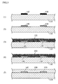
- FIG. 1 is a simplified sectional perspective view of part of the PDP according to the present invention.
- FIG. 2 is a magnified sectional view of a part of the PDP in FIG. 1, viewed along the x axis;
- FIG. 3 is a diagram illustrating a conventional production process for forming a PDP front panel, progressing in steps from ( 1 ) to ( 5 );
- FIG. 4 is a graph showing the time-temperature relationship for a conventional baking process of a PDP front panel
- FIG. 5 is a diagram illustrating the production process for forming a PDP front panel according to the present invention, progressing in steps from ( 1 ) to ( 5 );
- FIG. 6 is a graph showing the time-temperature relationship for the baking process of a PDP front panel according to the present invention.
- FIG. 7 is a magnified sectional view of part of a PDP, illustrating the specific locations for measuring silver and sodium content in the embodiment and the comparison samples.
- FIG. 8 is a play view illustrating part of the PDP front panel according to a modification of the preferred embodiment.
- FIG. 1 is a sectional perspective view of part of the display area of a PDP according to the present invention
- FIG. 2 is a sectional view along the y-z axis of address electrode 17 in FIG. 1 .
- a PDP is composed of a front panel 10 , and a back panel 20 , which face each other.
- the front panel 10 has a front glass substrate 11 , display electrodes 13 and 14 , a dielectric layer 15 , and a protective layer 16 .
- On the opposite face from the front glass substrate 11 are a plurality of pairs of intersecting display electrodes 13 and 14 .
- the dielectric layer 15 and protective layer 16 are applied as coatings to cover each electrode surface.
- the front glass substrate 11 is a planar sheet of soda-lime-borosilicate glass, which contains 2.5 wt % of sodium. There is no specified limit for the content of sodium, but up to 15 wt % is commercially available, so a higher content is desirable in consideration of cost.
- the display electrodes 13 and 14 both have silver as their principal ingredient (herein, “principal ingredient” means the element composes at least 50 wt % of the body).
- the dielectric layer 15 is formed as a coating over, and serves to insulate the display electrodes 13 and 14 .
- the dielectric layer 15 is composed of a glass material, such as a lead-oxide glass compound of lead oxide, boric oxide, silicon oxide, and aluminum oxide, or a bismuth-oxide glass compound of bismuth oxide, zinc oxide, boric oxide, silicon oxide and calcium oxide.
- the protective layer 16 is formed as a coating over the surface of the dielectric layer 15 , and includes ingredients such as magnesium oxide (MgO).
- the display electrodes 13 and 14 and the dielectric layer 15 are formed by simultaneous baking, resulting in reduced yellowing in the front glass substrate 11 .
- the back panel 20 is composed of the back glass substrate 21 , address electrodes 22 , a visible light reflecting layer 23 , barrier ribs 24 , and phosphor layers 25 R, 25 G and 25 B.
- the back glass substrate 21 is a planar sheet of soda-lime borosilicate glass, similar to the front glass substrate 11 , which contains 2.5 wt % of sodium.
- the back glass substrate 21 has address electrodes 22 arranged in a stripe pattern on the surface facing the front glass substrate 11 .
- the address electrodes 22 similar to the display electrodes 13 and 14 above, have silver as their principal ingredient, and are covered with a coating which forms the visible light reflecting layer 23 .
- the visible light reflecting layer 23 is a layer of dielectric glass, such as the dielectric layer 15 of the front glass substrate 11 , with titanium oxide added.
- the visible light reflecting layer 23 combines the functions of reflecting visible light emitted from the phosphor layers 25 R, 25 B and 25 G, and that of a dielectric layer.
- the barrier ribs 24 are arranged in rows on the surface of the visible light reflecting layer 23 , parallel to the address electrodes 22 . Between the barrier ribs 24 are phosphor layers 25 R, 25 G and 25 B, to which are applied phosphor particles, which emit red, green and blue light, respectively.
- a PDP is composed of a front panel 10 and a back panel 20 , which face each other and are sealed together around their perimeter by an airtight seal layer.
- the discharge space 26 created between the panels is filled with a discharge gas (such as a mixture of 95 vol % neon and 5 vol % xenon) at a certain pressure (such as 66.5 kPa).
- the PDP production method of the present invention is characterized by the baking process for the electrodes, dielectric layer and visible light reflecting layer of the front and back panels.
- the process for producing the electrodes and dielectric layer of the front panel is substantially similar to that of the electrodes and visible light reflecting layer of the back panel, so the front panel is taken as a representative example.
- FIG. 3 ( 1 ) through ( 5 ) show a partial sectional view of a conventional front panel as it moves through the production process.
- FIG. 4 is a graph showing the relationship between temperature and time for baking a front panel.
- silver paste which has silver as its principal ingredient and also contains glass flit, resin and solvent, is patterned onto the front glass substrate 110 by a thick-film screen-printing method.
- temperature is raised, as shown in FIG. 4, from ambient B 1 to temperature B 2 (e.g., 580° C.), which is equal to or higher than the softening point of the glass flit.
- This baking temperature is maintained at B 2 for a given period (t 1 to t 2 ), to decompose the resin in the silver paste, fuse the silver and glass flit, and form the display electrodes 130 and 140 .
- temperature is slowly lowered from B 2 to B 1 , from time t 2 to t 3 .
- ion exchange occurs at the interface the display electrodes 130 and the front glass substrate 110 , between the silver contained in the display electrodes 130 and 140 and the sodium contained in the front glass substrate 110 . Some of the silver ion is diffused into the front glass substrate 110 .
- a glass paste containing a mixture of low-melting flit glass powder, binder resin and solvent, is applied by a thick-film screen-printing method to the front glass substrate 110 over the display electrodes 130 and 140 . Drying of the solvent creates a coating of glass paste, as shown in FIG. 3 ( 4 ), forming the dielectric layer 150 .
- the front panel is heated again from ambient temperature B 1 to equal to or higher than the softening point of the glass flit contained in the glass paste (e.g., 580° C., from t 4 to t 5 ), and maintained there for a given time (t 5 to t 6 ).
- this baking decomposes the resin contained in the glass paste and fuses the glass flit.
- temperature is slowly lowered (time t 6 to t 7 ), forming the dielectric layer 150 .
- the protective layer is formed as a coating on the surface of the dielectric layer 150 , completing the front panel.
- ion exchange occurs between silver contained in the display electrodes 130 and 140 and sodium contained in the front glass substrate 110 . More silver ion is diffused into the front glass substrate 110 , and sodium ion is diffused into the dielectric layer 150 as well.
- a conventional back panel has address electrodes instead of the display electrodes 130 and 140 , a visible light reflection layer instead of the dielectric layer 150 , and barrier ribs and phosphor layers are formed. Otherwise, production is equivalent to the description above.
- the concentration of diffused silver in a front glass substrate after two bakings is higher than 0.8 wt %, or approximately 0.88 wt %.
- FIG. 5 ( 1 ) through ( 5 ) is a partial sectional view of a front panel as it moves through the production process according to the present invention.
- FIG. 6 is a graph showing the relationship between temperature and time for baking a front panel according to the present invention.
- silver paste which has silver as its principal ingredient and also contains glass flit, resin and solvent, is patterned onto the front glass substrate 11 by a thick-film screen-printing method and dried.
- the combined proportion of silver and glass flit is at least 90 wt % of the silver paste. If the proportion is less than 90 wt %, the silver paste loses viscosity, and the desired shape may not be obtained when the paste is applied to the front glass substrate 11 .
- a silver content in the paste of from 85 wt % to 95 wt % is desirable. Lower than 85 wt % creates increased shrinkage at baking, resulting in a less dense and less solid display electrode. A percentage higher than 95 wt % produces a higher viscosity silver paste, which creates inconsistencies in the thickness of the coating applied to the front panel 10 , and an uneven electrode after baking.
- the softening point of the glass flit is in the range of 300° to 350° C.
- a lower softening point results in premature softening, hindering resin decomposition.
- a higher softening point may result in insufficient contact bonding between the display electrode and the front glass substrate.
- a proportion of 1 wt % to 10 wt % of glass flit in the paste is desirable. Glass flit content of less than 1 wt % results in reduced adhesion to the front glass substrate, while more than 10 wt % can hinder decomposition of resin in the paste at baking.
- a resin which is easily decomposed by baking that is a resin which begins to decompose in air in the range of 350° to 500° C. is desirable, such as polymethyl methacrylate, ethyl cellulose, nitro cellulose, etc. Further, selection of a resin that completes decomposition at a lower temperature than the softening point of the glass in the dielectric layer 15 is desirable. This allows decomposition of the resin contained in the display electrodes 13 and 14 before fusing and hardening of the dielectric layer 15 , preventing bubbles from being trapped in the electrodes.
- the resin in order to achieve the proper viscosity when the silver paste is applied, should be held within a range of 1 wt % to 10 wt % of the silver paste.
- resin content When resin content is less than 1 wt %, the silver paste loses viscosity, and may cause difficulty in maintaining the desired electrode shape.
- resin content When resin content is greater than 10 wt %, the silver paste becomes extremely viscous, and causes inconsistencies when applied to the glass substrate.
- the temperatures for starting and completing decomposition given above are values measured using a TG-DTA (thermogravimetric-differential thermal analysis) apparatus with a temperature-gain rate of 10° C. per minute.
- an alcohol such as ethylene glycol, a terpene such as terpineol, a ketone such as methylethyl ketone, an ether such as carbitol, or other such compound is used.
- the thermal coefficient of expansion of the compound of silver and glass flit in the silver paste is desirable for the thermal coefficient of expansion of the compound of silver and glass flit in the silver paste to be within the range of 75 ⁇ 10 ⁇ 7 /K to 85 ⁇ 10 ⁇ 7 /K. This results in similar ranges for the display electrodes 13 and 14 and the front glass substrate 11 , reducing stress at the interface of the display electrodes and substrate during baking, and thereby reducing flaking.
- a thick-film screen-printing or a dye-coating technique is used to apply a glass material, composed of lead-oxide glass or bismuth-oxide glass, and glass paste, composed of resin and solvent, so as to cover the display electrodes 13 and 14 applied in the process above.
- this glass material has a higher softening point than the glass flit used above, and the resin in the glass paste begins to decompose at a lower temperature.
- a constant temperature dryer, or other device is used to vaporize the solvent contained in the paste.
- Step 1 (Time t 10 to t 11 )
- the front panel is placed in a baking furnace, and temperature is raised at a rate of from 5° to 20° C./minute to temperature A 2 , which is at least as high as the temperature at which the resin contained in the paste forming the display electrodes 13 and 14 and the dielectric layer 15 begins to decompose (about 200° C. for methyl meta-acrylate).
- temperature A 2 which is at least as high as the temperature at which the resin contained in the paste forming the display electrodes 13 and 14 and the dielectric layer 15 begins to decompose (about 200° C. for methyl meta-acrylate).
- Step 2 (Time t 11 to t 12 )
- temperature rise is slowed to below 5° C./minute or stopped and held constant. Temperature is maintained in the range equal to or higher than the softening point of the glass flit contained in the silver paste and equal to or lower than the softening point of the glass material contained in the glass paste.
- the decomposition temperature of the resin in the glass paste is lower than that of the resin in the silver paste forming the display electrodes 13 and 14 , already at this point the resin in the glass paste is decomposed almost completely.
- the vaporized resin escapes through the voids between glass particles, and the supply of oxygen increases, aiding the decomposition process of the resin in the silver paste.
- bubbles formed when the display electrodes 13 and 14 soften can pass through these voids and escape, reducing of air pockets in the finished electrodes. Therefore, the display electrodes 13 and 14 formed are dense and highly conductive.
- a reagent gas such as oxygen can be provided inside the baking furnace, which promotes oxidation of the resin.
- Providing a dry gas atmosphere accelerates baking by removing water produced by combustion of resin. Both techniques allow for more complete decomposition of the resin in the paste.
- metals such as silver oxidize easily, oxidation can be prevented by using hydrogen or another gas to create a reductant gas atmosphere in the baking furnace.
- a low-pressure atmosphere can be created in the baking furnace to prevent formation of air pockets in the display electrodes 13 and 14 , quickly removing from inside the furnace any gases emitted from the decomposing resin. It is desirable to maintain this low-pressure atmosphere continuously throughout Step 2 , but even momentary imposition can reduce formation of air pockets.
- Step 3 (Time t 12 to t 13 )
- temperature is again raised, to a temperature A 3 , equal to or higher than the softening point of the glass in the dielectric layer, at a given rate (e.g., 5° to 20° C./minute).
- Step 4 (Time t 13 to t 14 )
- Rate of temperature rise is reduced to below that of Step 3 , such as below 5° C./minute or stopped and held constant.
- Temperature is maintained in the range (temperature A 3 ) equal to or higher than the softening point of the glass material contained in the glass paste. As shown in FIG. 5 ( 5 ), this fuses the glass particles 151 contained in the glass paste, and results in the formation of a dielectric layer 15 with a dense structure.
- Step 5 (Time t 14 to t 15 )
- the hot front panel is cooled to ambient temperature. Cooling is done slowly, in order to prevent formation of cracks in the dielectric layer 15 and display electrodes 13 and 14 .
- the front panel is removed from the baking furnace, and a protective layer is formed as a MgO coating applied over the dielectric layer 15 surface by CVD or other technique. This completes the formation of the front panel 10 .
- the front panel's electrodes and dielectric layer can be formed with only one baking.
- This shortening of baking time compared with conventional methods suppresses diffusion of silver into the front glass substrate, limiting concentration of diffused silver measured in an area of the glass substrate with a diameter of 5 ⁇ m centered 7.5 ⁇ m from the interface of the electrode and the substrate to 0.8 wt % or less, lower than that of panels produced by conventional methods.
- the back panel 20 has address electrodes 22 formed in rows on the back glass substrate 21 by a screen printing technique using the same silver paste as the front panel electrodes.
- the visible light reflecting layer 23 is formed over the electrodes, also by a screen printing technique using the same glass paste as for the dielectric layer 15 above, with titanium oxide added.
- the address electrodes 22 and visible light reflecting layer 23 are baked by the same procedure as described above. Then a paste containing lead glass material is applied repeatedly at a given pitch by a screen printing technique and baked to form the barrier ribs 24 .
- the discharge space 26 is divided into cells in the direction of the x-axis by the barrier ribs 24 .
- baking of the address electrodes 22 and visible light reflecting layer 23 may be done all at once after printing of the barrier ribs 24 .
- a phosphor ink paste composed of red, green and blue phosphor particles and an organic binder, is applied in the channels formed between the barrier ribs 24 .
- the organic binder is combusted, and the phosphor particles are fused to form the phosphor layers 25 R, 25 G and 25 B.
- the front panel 10 and back panel 20 are joined so that the display electrodes 13 and 14 are perpendicular to the address electrodes 22 .
- the panels are sealed together by a sealing glass material applied around their outer edges and baked about 450° C. for 10 to 20 minutes to form an airtight seal.
- the discharge space 26 is evacuated (e.g., to 1.1 ⁇ 10 ⁇ 4 Pa), then filled with a discharge gas (e.g., He—Xe- or Ne—Xe-type inert gas) at a given pressure to complete the PDP.
- a discharge gas e.g., He—Xe- or Ne—Xe-type inert gas
- the front panel 10 and back panel 20 can be produced with fewer bakings than by conventional methods, reducing the amount of silver diffused into the front glass substrate 11 .
- yellowing and reduction of color balance in the finished PDP are controlled.
- Formation of air pockets in the display electrodes 13 and 14 is also controlled, providing display electrodes with a dense, fine texture and excellent conductivity. Reduction of repetitive baking also saves time and energy in the production process, allowing cost to reduced as well.
- a PDP front panel was produced by the method disclosed above and shown in FIGS. 5 and 6, as a sample of the preferred embodiment.
- a PDP front panel was produced by the method disclosed above and shown in FIGS. 3 and 4, as a sample of conventional methods for comparison.
- FIG. 7 a partial sectional view of a front panel, shows the locations where measurements were taken, specifically, in an area P 1 of the front glass substrate 11 with a diameter of 5 ⁇ m centered 7.5 ⁇ m from the interface of a display electrode 13 ( 14 ) and the substrate.
- the content of diffused silver at P 1 in the embodiment sample is 0.73 wt %, about 17% lower than the comparison sample measurement of 0.88 wt %.
- a lower value here is desirable as it means yellowing of the substrate is reduced.
- the embodiment of the current invention produces a value lower than 0.80 wt %.
- sodium moves from the front glass substrate into the dielectric layer by ion exchange.
- 2.70 wt % of sodium measured in the embodiment sample is only slightly less than the 2.96 wt % measured in the substrate before panel formation.
- the concentration of sodium in the substrate before panel formation can be used as a representative for the concentration in the side of the front glass substrate opposite from the electrodes after formation of the panel.
- the embodiment sample shows lower amounts of diffused silver and sodium than the comparison sample.
- 0.20 wt % of sodium at P 2 of the embodiment sample is smaller than the 0.33 wt % measured in the comparison sample, indicating that silver and sodium ion exchange is suppressed in the embodiment sample.
- a lower value here is desirable as it means yellowing of the panel is reduced.
- the embodiment of the current invention produces a value lower than 0.25 wt %.
- the amount of diffused silver in the embodiment sample, 0.33 wt % is lower than the comparison sample measurement of 0.48 wt %.
- a lower value here is desirable as it means yellowing of the panel is reduced.
- the embodiment of the current invention produces a value lower than 0.4 wt %.
- the embodiment sample ratio of 0.45 is lower than the comparison sample ratio of 0.54.
- a value of 0.5 or lower here is desirable as it means panel yellowing and dielectric layer breakdown are limited. That is, by obtaining a value of 0.5 or lower, silver diffusion into the dielectric layer and yellowing of the panel are limited, and dielectric breakdown by diffusion of conductive silver into the dielectric layer can also be suppressed.
- the preferred embodiment above has display electrodes formed in lines on the front glass substrate, but the present invention can also be embodied in a panel with electrodes of a different shape.
- the PDP of this modification example has substantially the same structure as that of the preferred embodiment above, except for the display electrodes. As shown in FIG. 8, a plan view of the essential portion of the front panel, display electrodes 230 and 240 are arranged side by side in parallel to each other.
- Display electrode 230 is composed of line units 231 and 232 , which are spaced apart and parallel, connected by a plurality of bridge units 233 (this structure is referred to below as a “fence shape”). The display electrode 230 is in direct contact with the front glass substrate across the display area.
- Display electrode 240 is composed of line units 241 and 242 and bridge units 243 , structured in a fence shape like the display electrode 230 .
- Each display electrode 230 and 240 can be formed by the same method as the preferred embodiment above, using a screen-printing technique to apply silver paste to the front glass substrate in the fence shape.
Landscapes
- Engineering & Computer Science (AREA)
- Manufacturing & Machinery (AREA)
- Physics & Mathematics (AREA)
- Plasma & Fusion (AREA)
- Gas-Filled Discharge Tubes (AREA)
Priority Applications (1)
| Application Number | Priority Date | Filing Date | Title |
|---|---|---|---|
| US10/423,219 US6913501B2 (en) | 2000-03-31 | 2003-04-25 | Display panel production method |
Applications Claiming Priority (2)
| Application Number | Priority Date | Filing Date | Title |
|---|---|---|---|
| JP2000097306 | 2000-03-31 | ||
| JP2000-097306 | 2000-03-31 |
Related Child Applications (1)
| Application Number | Title | Priority Date | Filing Date |
|---|---|---|---|
| US10/423,219 Division US6913501B2 (en) | 2000-03-31 | 2003-04-25 | Display panel production method |
Publications (2)
| Publication Number | Publication Date |
|---|---|
| US20030071572A1 US20030071572A1 (en) | 2003-04-17 |
| US6614184B2 true US6614184B2 (en) | 2003-09-02 |
Family
ID=18611941
Family Applications (2)
| Application Number | Title | Priority Date | Filing Date |
|---|---|---|---|
| US09/824,466 Expired - Fee Related US6614184B2 (en) | 2000-03-31 | 2001-04-02 | Display panel and display panel production method |
| US10/423,219 Expired - Fee Related US6913501B2 (en) | 2000-03-31 | 2003-04-25 | Display panel production method |
Family Applications After (1)
| Application Number | Title | Priority Date | Filing Date |
|---|---|---|---|
| US10/423,219 Expired - Fee Related US6913501B2 (en) | 2000-03-31 | 2003-04-25 | Display panel production method |
Country Status (3)
| Country | Link |
|---|---|
| US (2) | US6614184B2 (zh) |
| KR (1) | KR20010095198A (zh) |
| CN (2) | CN1595586A (zh) |
Cited By (3)
| Publication number | Priority date | Publication date | Assignee | Title |
|---|---|---|---|---|
| US20050022854A1 (en) * | 2003-07-28 | 2005-02-03 | Weidan Wu | Party tent |
| US20060049763A1 (en) * | 2004-09-07 | 2006-03-09 | Chunghwa Picture Tubes., Ltd | Structure of flat gas discharge lamp |
| US8164261B2 (en) * | 2010-02-22 | 2012-04-24 | Panasonic Corporation | Plasma display panel |
Families Citing this family (15)
| Publication number | Priority date | Publication date | Assignee | Title |
|---|---|---|---|---|
| JP2004095355A (ja) * | 2002-08-30 | 2004-03-25 | Pioneer Electronic Corp | ディスプレイパネルの製造方法 |
| JP3972021B2 (ja) * | 2003-05-28 | 2007-09-05 | 東京応化工業株式会社 | プラズマディスプレイ前面板製造用未焼成積層体およびプラズマディスプレイ前面板の製造方法 |
| KR100515323B1 (ko) * | 2003-07-30 | 2005-09-15 | 삼성에스디아이 주식회사 | 플라즈마 디스플레이 패널 |
| JP2005322444A (ja) * | 2004-05-06 | 2005-11-17 | Hitachi Ltd | 表示パネル用基板構体の作製材料及び表示パネル用基板構体の作製方法 |
| JP2006222035A (ja) * | 2005-02-14 | 2006-08-24 | Fujitsu Hitachi Plasma Display Ltd | プラズマディスプレイパネル |
| KR20060113137A (ko) * | 2005-04-29 | 2006-11-02 | 엘지전자 주식회사 | 플라즈마 디스플레이 패널 및 그 제조방법 |
| KR101169049B1 (ko) * | 2005-06-30 | 2012-07-26 | 엘지디스플레이 주식회사 | 액정 표시 장치용 박막 트랜지스터 소자 및 그의 제조 방법 |
| JP4089739B2 (ja) * | 2005-10-03 | 2008-05-28 | 松下電器産業株式会社 | プラズマディスプレイパネル |
| KR100759666B1 (ko) * | 2006-01-27 | 2007-09-17 | 삼성에스디아이 주식회사 | 평판 표시장치 및 그의 제조방법 |
| KR100688792B1 (ko) * | 2006-01-27 | 2007-03-02 | 삼성에스디아이 주식회사 | 평판 표시장치 및 그의 제조방법 |
| JP4089733B2 (ja) * | 2006-02-14 | 2008-05-28 | 松下電器産業株式会社 | プラズマディスプレイパネル |
| KR20110097834A (ko) * | 2008-11-17 | 2011-08-31 | 휴렛-팩커드 디벨롭먼트 컴퍼니, 엘.피. | 표면 증강 라만 산란을 위한 기판 |
| EP2459975A4 (en) * | 2009-07-30 | 2013-10-23 | Hewlett Packard Development Co | NANODRAHT BASED SYSTEMS FOR RAMAN SPECTROSCOPY |
| CN103322512B (zh) * | 2013-05-22 | 2014-08-06 | 深圳市绎立锐光科技开发有限公司 | 一种荧光粉片及其制备方法、相关发光装置 |
| US9287379B2 (en) | 2014-05-19 | 2016-03-15 | Micron Technology, Inc. | Memory arrays |
Citations (3)
| Publication number | Priority date | Publication date | Assignee | Title |
|---|---|---|---|---|
| JPH11329236A (ja) | 1998-05-06 | 1999-11-30 | Toray Ind Inc | プラズマディスプレイ用基板の製造方法 |
| US6097149A (en) * | 1997-03-31 | 2000-08-01 | Mitsubishi Denki Kabushiki Kaisha | Plasma display panel with bus electrodes having black electroconductive material |
| US6457408B1 (en) * | 1994-11-25 | 2002-10-01 | Canon Kabushiki Kaisha | Producing surface conduction electron emitting device with offset printed electrodes |
Family Cites Families (9)
| Publication number | Priority date | Publication date | Assignee | Title |
|---|---|---|---|---|
| JP2963464B2 (ja) * | 1989-06-15 | 1999-10-18 | 富士通株式会社 | プラズマディスプレイパネルの製造方法 |
| JPH09245652A (ja) * | 1996-03-13 | 1997-09-19 | Dainippon Printing Co Ltd | プラズマディスプレイパネルの電極及びその形成方法 |
| JPH10302648A (ja) * | 1997-04-30 | 1998-11-13 | Asahi Glass Co Ltd | プラズマディスプレイ用ガラス基板 |
| DE69935882T2 (de) * | 1998-05-12 | 2007-09-06 | Matsushita Electric Industrial Co., Ltd., Kadoma | Herstellungsverfahren einer Plasmaentladungs-Anzeigeplatte |
| US6437505B1 (en) * | 1998-11-30 | 2002-08-20 | Thomson Licensing S.A. | Coplanar-type plasma panel with improved matrix structure arrangement |
| JP2000226233A (ja) * | 1999-02-04 | 2000-08-15 | Asahi Glass Co Ltd | フラットパネルディスプレイ基板用フロートガラス |
| JP2001160361A (ja) * | 1999-09-21 | 2001-06-12 | Mitsubishi Electric Corp | プラズマディスプレイパネル用基板及びプラズマディスプレイパネル |
| JP3389240B2 (ja) * | 1999-12-21 | 2003-03-24 | 松下電器産業株式会社 | プラズマディスプレイパネルおよびその製造方法 |
| KR100551522B1 (ko) * | 2002-12-11 | 2006-02-13 | 파이오니아 가부시키가이샤 | 플라즈마 디스플레이 패널의 소성로 및 플라즈마디스플레이 패널의 제조 방법 |
-
2001
- 2001-03-31 KR KR1020010017093A patent/KR20010095198A/ko not_active Application Discontinuation
- 2001-03-31 CN CNA2004100835661A patent/CN1595586A/zh active Pending
- 2001-03-31 CN CNB011178019A patent/CN1183497C/zh not_active Expired - Fee Related
- 2001-04-02 US US09/824,466 patent/US6614184B2/en not_active Expired - Fee Related
-
2003
- 2003-04-25 US US10/423,219 patent/US6913501B2/en not_active Expired - Fee Related
Patent Citations (3)
| Publication number | Priority date | Publication date | Assignee | Title |
|---|---|---|---|---|
| US6457408B1 (en) * | 1994-11-25 | 2002-10-01 | Canon Kabushiki Kaisha | Producing surface conduction electron emitting device with offset printed electrodes |
| US6097149A (en) * | 1997-03-31 | 2000-08-01 | Mitsubishi Denki Kabushiki Kaisha | Plasma display panel with bus electrodes having black electroconductive material |
| JPH11329236A (ja) | 1998-05-06 | 1999-11-30 | Toray Ind Inc | プラズマディスプレイ用基板の製造方法 |
Cited By (3)
| Publication number | Priority date | Publication date | Assignee | Title |
|---|---|---|---|---|
| US20050022854A1 (en) * | 2003-07-28 | 2005-02-03 | Weidan Wu | Party tent |
| US20060049763A1 (en) * | 2004-09-07 | 2006-03-09 | Chunghwa Picture Tubes., Ltd | Structure of flat gas discharge lamp |
| US8164261B2 (en) * | 2010-02-22 | 2012-04-24 | Panasonic Corporation | Plasma display panel |
Also Published As
| Publication number | Publication date |
|---|---|
| US6913501B2 (en) | 2005-07-05 |
| US20030201717A1 (en) | 2003-10-30 |
| CN1183497C (zh) | 2005-01-05 |
| CN1320897A (zh) | 2001-11-07 |
| KR20010095198A (ko) | 2001-11-03 |
| US20030071572A1 (en) | 2003-04-17 |
| CN1595586A (zh) | 2005-03-16 |
Similar Documents
| Publication | Publication Date | Title |
|---|---|---|
| US6614184B2 (en) | Display panel and display panel production method | |
| KR100254479B1 (ko) | 플라즈마 디스플레이판넬 및 그 제조방법 | |
| JP2003115261A (ja) | ディスプレイパネルの製造方法 | |
| JP2001151532A (ja) | 電極被覆用低融点ガラスおよびプラズマディスプレイ装置 | |
| KR100878935B1 (ko) | 플라즈마 디스플레이 패널 | |
| JP2002056775A (ja) | プラズマディスプレイパネル用基板の製造方法、プラズマディスプレイパネル用基板及びプラズマディスプレイパネル | |
| JP3363141B2 (ja) | ディスプレイパネルおよびその製造方法 | |
| KR20060116117A (ko) | 플라즈마 디스플레이 패널의 제조방법 | |
| JPH09199037A (ja) | Ac型プラズマディスプレイパネル | |
| JP3846636B2 (ja) | プラズマディスプレイパネル及びその製造方法 | |
| JP2004247211A (ja) | 厚膜シート電極の製造方法 | |
| KR100831009B1 (ko) | 플라스마 디스플레이 패널 | |
| JP3946241B2 (ja) | プラズマディスプレイパネル及びその製造方法 | |
| EP1367621A1 (en) | Plasma display panel and method for manufacture thereof | |
| CN101341569B (zh) | 平面型显示装置 | |
| KR100696634B1 (ko) | 가스 방전 표시 장치 및 그 제조 방법 | |
| JP3965974B2 (ja) | プラズマディスプレイパネルおよびその製造方法 | |
| JP2000243303A (ja) | 放電型表示装置の背面側基板の構造 | |
| JP4197190B2 (ja) | プラズマディスプレイパネル | |
| JP2000123743A (ja) | プラズマディスプレイパネル | |
| JP2008027800A (ja) | プラズマディスプレイパネルの誘電体層を形成する方法 | |
| JP4162692B2 (ja) | プラズマディスプレイパネル | |
| JP2008103217A (ja) | プラズマディスプレイパネル | |
| JPH0353429A (ja) | プラズマディスプレイパネルの製造方法 | |
| KR100823203B1 (ko) | 플라즈마 디스플레이 소자의 전면판 구조 및 그 제조방법 |
Legal Events
| Date | Code | Title | Description |
|---|---|---|---|
| AS | Assignment |
Owner name: MATSUSHITA ELECTRIC INDUSTRIAL CO., LTD., JAPAN Free format text: ASSIGNMENT OF ASSIGNORS INTEREST;ASSIGNORS:HIBINO, JUNICHI;SASAKI, YOSHIKI;YAMASHITA, KATSUYOSI;AND OTHERS;REEL/FRAME:011664/0759 Effective date: 20010321 |
|
| FEPP | Fee payment procedure |
Free format text: PAYOR NUMBER ASSIGNED (ORIGINAL EVENT CODE: ASPN); ENTITY STATUS OF PATENT OWNER: LARGE ENTITY |
|
| CC | Certificate of correction | ||
| FPAY | Fee payment |
Year of fee payment: 4 |
|
| FPAY | Fee payment |
Year of fee payment: 8 |
|
| REMI | Maintenance fee reminder mailed | ||
| LAPS | Lapse for failure to pay maintenance fees | ||
| STCH | Information on status: patent discontinuation |
Free format text: PATENT EXPIRED DUE TO NONPAYMENT OF MAINTENANCE FEES UNDER 37 CFR 1.362 |
|
| FP | Lapsed due to failure to pay maintenance fee |
Effective date: 20150902 |