US6426908B1 - Semiconductor memory device with reduced current consumption in data hold mode - Google Patents
Semiconductor memory device with reduced current consumption in data hold mode Download PDFInfo
- Publication number
- US6426908B1 US6426908B1 US09/511,927 US51192700A US6426908B1 US 6426908 B1 US6426908 B1 US 6426908B1 US 51192700 A US51192700 A US 51192700A US 6426908 B1 US6426908 B1 US 6426908B1
- Authority
- US
- United States
- Prior art keywords
- refresh
- circuit
- power supply
- address
- voltage
- Prior art date
- Legal status (The legal status is an assumption and is not a legal conclusion. Google has not performed a legal analysis and makes no representation as to the accuracy of the status listed.)
- Expired - Lifetime
Links
Images


Classifications
-
- G—PHYSICS
- G11—INFORMATION STORAGE
- G11C—STATIC STORES
- G11C11/00—Digital stores characterised by the use of particular electric or magnetic storage elements; Storage elements therefor
- G11C11/21—Digital stores characterised by the use of particular electric or magnetic storage elements; Storage elements therefor using electric elements
- G11C11/34—Digital stores characterised by the use of particular electric or magnetic storage elements; Storage elements therefor using electric elements using semiconductor devices
- G11C11/40—Digital stores characterised by the use of particular electric or magnetic storage elements; Storage elements therefor using electric elements using semiconductor devices using transistors
- G11C11/401—Digital stores characterised by the use of particular electric or magnetic storage elements; Storage elements therefor using electric elements using semiconductor devices using transistors forming cells needing refreshing or charge regeneration, i.e. dynamic cells
- G11C11/4063—Auxiliary circuits, e.g. for addressing, decoding, driving, writing, sensing or timing
- G11C11/407—Auxiliary circuits, e.g. for addressing, decoding, driving, writing, sensing or timing for memory cells of the field-effect type
-
- G—PHYSICS
- G11—INFORMATION STORAGE
- G11C—STATIC STORES
- G11C5/00—Details of stores covered by group G11C11/00
- G11C5/14—Power supply arrangements, e.g. power down, chip selection or deselection, layout of wirings or power grids, or multiple supply levels
-
- G—PHYSICS
- G11—INFORMATION STORAGE
- G11C—STATIC STORES
- G11C11/00—Digital stores characterised by the use of particular electric or magnetic storage elements; Storage elements therefor
- G11C11/21—Digital stores characterised by the use of particular electric or magnetic storage elements; Storage elements therefor using electric elements
- G11C11/34—Digital stores characterised by the use of particular electric or magnetic storage elements; Storage elements therefor using electric elements using semiconductor devices
- G11C11/40—Digital stores characterised by the use of particular electric or magnetic storage elements; Storage elements therefor using electric elements using semiconductor devices using transistors
- G11C11/401—Digital stores characterised by the use of particular electric or magnetic storage elements; Storage elements therefor using electric elements using semiconductor devices using transistors forming cells needing refreshing or charge regeneration, i.e. dynamic cells
- G11C11/406—Management or control of the refreshing or charge-regeneration cycles
-
- G—PHYSICS
- G11—INFORMATION STORAGE
- G11C—STATIC STORES
- G11C11/00—Digital stores characterised by the use of particular electric or magnetic storage elements; Storage elements therefor
- G11C11/21—Digital stores characterised by the use of particular electric or magnetic storage elements; Storage elements therefor using electric elements
- G11C11/34—Digital stores characterised by the use of particular electric or magnetic storage elements; Storage elements therefor using electric elements using semiconductor devices
- G11C11/40—Digital stores characterised by the use of particular electric or magnetic storage elements; Storage elements therefor using electric elements using semiconductor devices using transistors
- G11C11/401—Digital stores characterised by the use of particular electric or magnetic storage elements; Storage elements therefor using electric elements using semiconductor devices using transistors forming cells needing refreshing or charge regeneration, i.e. dynamic cells
- G11C11/4063—Auxiliary circuits, e.g. for addressing, decoding, driving, writing, sensing or timing
- G11C11/407—Auxiliary circuits, e.g. for addressing, decoding, driving, writing, sensing or timing for memory cells of the field-effect type
- G11C11/4074—Power supply or voltage generation circuits, e.g. bias voltage generators, substrate voltage generators, back-up power, power control circuits
-
- G—PHYSICS
- G11—INFORMATION STORAGE
- G11C—STATIC STORES
- G11C5/00—Details of stores covered by group G11C11/00
- G11C5/14—Power supply arrangements, e.g. power down, chip selection or deselection, layout of wirings or power grids, or multiple supply levels
- G11C5/143—Detection of memory cassette insertion or removal; Continuity checks of supply or ground lines; Detection of supply variations, interruptions or levels ; Switching between alternative supplies
-
- G—PHYSICS
- G11—INFORMATION STORAGE
- G11C—STATIC STORES
- G11C2211/00—Indexing scheme relating to digital stores characterized by the use of particular electric or magnetic storage elements; Storage elements therefor
- G11C2211/401—Indexing scheme relating to cells needing refreshing or charge regeneration, i.e. dynamic cells
- G11C2211/406—Refreshing of dynamic cells
- G11C2211/4061—Calibration or ate or cycle tuning
Definitions
- the present invention relates generally to semiconductor devices, and in particular to configurations for reducing the current consumed in a refresh mode for holding data, such as a sleep mode or a power down mode, without causing an erroneous operation in a semiconductor memory device requiring refreshing of storage data. More specifically, the present invention relates to a configuration for reducing the current consumed in a refresh mode by a logic merged memory with a logic and a dynamic random access memory integrated on a single semiconductor chip.
- a conventional CMOS semiconductor device is reduced in transistor size, in particular, gate length of a MOS transistor (an insulated gate field effect transistor) to achieve high density and high integration. While a reduced power supply voltage is employed to ensure the reliability of such a microfabricated transistor and reduce the power consumption of the device, in order to achieve fast operation the MOS transistor is required to have a threshold voltage Vth reduced in absolute value as an operating power supply voltage is reduced.
- MOS transistor an insulated gate field effect transistor
- a MOS transistor conducts a current referred to as a sub threshold leakage current (referred to as an “off leak current” hereinafter) between its source and drain even when it is turned off.
- an off leak current When a threshold voltage is reduced in absolute value, an increased off leak current flows. Since an absolute value of a threshold voltage has a negative temperature-dependency and thus reduces as temperature rises, an increased operating temperature causes an increased off leak current and hence an increased direct current in the entirety of a large scale integrated circuit.
- a current flowing in a standby state (a standby current) is disadvantageously increased.
- FIG. 60 shows an example of a conventional MT-CMOS configuration.
- cascaded CMOS inverters IV 1 -IV 5 of five stages are shown as an internal circuit.
- An input signal IN fed to the first-stage inverter IV 1 is at a low level in a standby cycle.
- CMOS inverters IV 1 -IV 5 have an identical configuration and each includes a p channel MOS transistor PT and an n channel MOS transistor NT.
- MOS transistors PT and NT each are a low threshold voltage (L-Vth) MOS transistor with its threshold voltage reduced in absolute value.
- L-Vth low threshold voltage
- a main power supply line 1 receiving a power supply voltage Vcc
- a sub power supply line 3 coupled with main power supply line 1 via a leakage-cutting p channel MOS transistor PQ
- a main ground line 2 transmitting a ground voltage Vss
- a sub ground line 4 connected to main ground line 2 via a leakage-cutting n channel MOS transistor NQ.
- Leakage-cutting MOS transistors PQ and NQ are an (M-Vth) MOS transistor which has a threshold voltage greater in absolute value than MOS transistors PT and NT have.
- MOS transistor PQ has its gate receiving a control signal / ⁇ and MOS transistor NQ has its gate receiving a control signal ⁇ .
- Control signal ⁇ attains a high level in an active cycle in which the internal circuit operates, and control signal ⁇ attains a low level in a standby cycle in which the internal circuit is set in a standby state.
- Control signal / ⁇ attains a low level in the active cycle and a high level in the standby cycle.
- odd-stage inverters IV 1 , IV 3 and IV 5 . . . have sources of their p channel MOS transistors PTs connected to main power supply line 1 and sources of n channel MOS transistors NTs connected to sub ground line 4 .
- Even-stage inverters IV 2 , IV 4 , . . . have sources of their p channel MOS transistors PTs connected to sub power supply line 3 and sources of their n channel MOS transistors NTs connected to main ground line 2 .
- control signal ⁇ is at a low level and control signal / ⁇ is at a high level, and input signal IN is at a low level.
- leakage cutting MOS transistors PQ and NQ are turned off.
- odd-stage inverters IV 1 , IV 3 , and IV 5 their p channel MOS transistors PTs are turned on and their n channel MOS transistors NTs are turned off, since input signal IN is at a low level.
- the p channel MOS transistors PTs have their sources connected to main power supply line 1 and the n channel MOS transistors NTs have their sources connected to sub ground line 4 .
- p channel MOS transistor PT transmits to a corresponding output node (or drain) a voltage of the power supply voltage Vcc level on main power supply line 1 , its source and drain voltages are equalized and the transistor does not conduct.
- Sub ground line 4 is connected to main ground line 2 via leakage cutting MOS transistor NQ having the relatively high threshold voltage M-Vth.
- leakage cutting MOS transistor NQ cannot discharge all of the off leak currents and a voltage level SVss on sub ground line 4 becomes higher than ground voltage Vss.
- the level of voltage SVss on sub ground line 4 is ultimately determined by a relationship between the amount of the leakage current discharged by leakage cutting MOS transistor NQ and the sum of all of the off leak currents from the inverter stages included in the internal circuit.
- even-stage inverters IV 2 , IV 4 . . . input signal IN is at a high level.
- Even-stage inverters IV 2 , IV 4 , . . . have their p channel MOS transistors PTs connected at the respective sources to sub power supply line 3 and their n channel MOS transistors NTs connected at the respective sources to main ground line 2 .
- Even-stage inverters IV 2 , IV 4 , . . . their n channel MOS transistors have their sources and drains both set at the ground voltage Vss level and thus do not conduct and cause no off leak current.
- the p channel MOS transistors PTs cause off leak current.
- leakage-cutting MOS transistor PQ is set to have a threshold voltage of a relatively large absolute value (M-Vth).
- M-Vth a threshold voltage of a relatively large absolute value
- the amount of the leakage current from main power supply line 1 to sub power supply line 3 is determined by leakage cutting MOS transistor PQ, and voltage SVcc on sub power supply line 3 becomes lower than the power supply voltage Vcc level.
- the voltage SVcc level on sub power supply line 3 is ultimately determined by a relationship between the leakage current from leakage cutting MOS transistor PQ and the sum of all of the off leak currents in even-stage inverters IV 2 , IV 4 , .
- in even-stage inverters IV 2 , IV 4 . . . their p channel MOS transistors PTs have the respective gates and respective sources reverse-biased, resulting in a further reduced off leak current.
- control signal ⁇ attains a high level and control signal/ ⁇ attains a low level, leakage cutting MOS transistors PQ and NQ are turned on, main power supply line 1 is connected to sub power supply line 3 , and main ground line 2 is connected to sub ground line 4 .
- voltage SVcc on sub power supply line 3 attains the power supply voltage Vcc level
- voltage SVss on sub ground line 4 attains the ground voltage Vss level.
- input signal IN varies with an operating state.
- the MOS transistors of inverters IV 1 -IV 5 . . . configuring the internal circuit are low threshold voltage MOS transistors and thus operate at high speed. Leakage cutting MOS transistors PQ and NQ have their current supplying ability set to a large value, in order to sufficiently guarantee the operation of the internal circuit.
- the power supply line/ground line has an impedance thereof increased to reduce a leakage current in the standby cycle, and in the active cycle the power supply line/ground line has an impedance thereof reduced to allow a fast operation owing to the low threshold voltage MOS transistors in the internal circuit.
- a semiconductor circuit device providing a reduced current consumption in the standby cycle and also operating at high speed in the active cycle is to be implemented.
- the conventional MT-CMOS configuration requires input signal IN to be set at a predetermined logic level in the standby cycle. According to the logic level of input signal IN in the standby cycle, it must be determined where the internal circuit's power supply and ground lines are connected. For a random logic and a register circuit storing data indicative of operating conditions and such, however, input signals IN cannot have a predetermined logic level in the standby cycle, and the MT-CMOS configuration as shown in FIG. 60 can not be employed.
- a semiconductor device is a dynamic semiconductor memory device (referred to as a DRAM hereinafter)
- DRAM when no access is made for a relatively long period of time and a sleep mode is set, DRAM is set to a self refresh mode. In the self refresh mode, the DRAM internally, periodically refreshes the data stored in memory cells.
- the DRAM When self refresh operation is in effect performed, the DRAM enters an active cycle, and when the refresh operation completes, the DRAM enters a standby cycle. That is, the DRAM in the self refresh mode enters the active cycle at predetermined intervals.
- the self refresh mode the data in memory cells are internally refreshed to merely hold the data. This results in a disadvantageous current consumption.
- a longer refresh interval is required.
- an unnecessarily long refresh interval results in the data in memory cells being destroyed before refresh operation is performed, and the data cannot be held.
- An object of the present invention is to provide a semiconductor device capable of reducing a current consumption in a standby state without degrading its fast operability.
- Another object of the present invention is to provide a semiconductor device capable of reducing a current consumption in a self refresh mode.
- Still another object of the present invention is to provide a semiconductor device capable of reducing a current consumption in a standby mode without negatively affecting its normal operation and data holding capability.
- the semiconductor device includes a plurality of memory cells requiring refreshing of the storage data within a predetermined period of time, refresh-related circuitry for performing an operation of refreshing the data stored in the plurality of memory cells in a refresh mode, peripheral circuitry different from the refresh-related circuitry and performing at least an operation related to accessing to the plurality of memory cells, a first power supply circuit for supplying an operating power supply voltage to the refresh-related circuitry, a second power supply circuit provided separately from the first power supply circuit for supplying an operating power supply voltage to the peripheral circuitry, and a power supply control circuit responsive to an operation mode designation signal for adjusting an impedance of at least the second power supply circuit.
- the power supply control circuit includes a circuit for setting the first and second power supply circuits into different voltage supplying states when the operation mode designation signal designates the refresh mode and for setting the first and second power supply circuits in the same voltage supplying state when the operation mode designation signal designates a normal mode different from the refresh mode.
- the semiconductor device includes a plurality of memory cells having their storage data refreshed within a predetermined period of time, a register circuit receiving a power supply voltage of a power source node for storing information related to an operation of accessing the plurality of memory cells, a register capacitor provided corresponding to the register circuit for holding information stored in the register circuit, and a control circuit for periodically refreshing information stored in the register capacitor when an operation mode designation signal designates a refresh mode.
- the semiconductor device includes a memory cell array of a plurality of memory cells having a predetermined storage capacity and having the data stored therein refreshed within a predetermined period of time, a circuit for receiving and storing an address designating a refresh region to be refreshed when a refresh mode of performing a refresh operation is designated in response to an operation mode designation signal, a refresh address generation circuit for generating a refresh address to address a memory cell to be refreshed in a region designated by the refresh region designating address when the operation mode designation signal designates the refresh mode, a refresh timer outputting a refresh request requesting refreshing of the data stored in the memory cells at a predetermined period, and refresh-related circuitry responsive to the refresh request from the refresh timer for refreshing the data stored in the memory cells of the refresh address.
- the refresh-related circuitry and the peripheral circuitry can both receive a power supply voltage to prevent the power supply voltage from varying upon switching between an active cycle and a standby cycle, so that an internal circuit can start to operate at a fast timing.
- periodical refreshing of the information stored in the register capacitor holding the data of the register circuit allow power supply to the register circuit to be intermittently stopped in the refresh mode, resulting in reduced current consumption in the refresh mode.
- refreshing of memory cells only in a predetermined address region allows the number of memory cell rows refreshed or the frequency of refresh operations to be reduced to implement a reduced current consumption.
- FIG. 1 schematically shows an entire configuration of a semiconductor device according to the present invention.
- FIG. 2 schematically shows a configuration of a semiconductor device according to a first embodiment of the present invention.
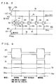
- FIG. 3 schematically shows a configuration of a power supply circuit for the column-related/peripheral control circuitry shown in FIG. 2 .
- FIG. 4 is a signal waveform diagram representing an operation of the power supply circuit shown in FIG. 3 .
- FIG. 5 schematically shows a configuration of a power supply circuit for the logic circuit shown in FIG. 2 .
- FIG. 6 is a signal waveform diagram representing an operation of the power supply circuit shown in FIG. 5 .
- FIG. 7 schematically shows another configuration of the power supply circuit for the logic circuit shown in FIG. 2 .
- FIG. 8 shows a configuration of a first modification of the power supply circuit for the peripheral circuitry according to the fist embodiment of the present invention.
- FIG. 9 schematically shows a configuration of a first modification of the power supply circuit for the logic circuit according to the first embodiment of the present invention.
- FIG. 10 shows a configuration of a second modification of the power supply circuit for the peripheral circuitry of the first embodiment of the present invention.
- FIG. 11 schematically shows a configuration of a power supply control circuit for the power supply circuit shown in FIG. 10 .
- FIG. 12 is a signal waveform diagram representing an operation of the power supply control circuit shown in FIG. 11 .
- FIG. 13 shows a configuration of a third modification of the power supply circuit for the peripheral circuitry according to the first embodiment of the present invention.
- FIG. 14 schematically shows a configuration of a power supply control circuit for the power supply circuit shown in FIG. 13 .
- FIG. 15 is a signal waveform diagram representing an operation of the power supply control circuit shown in FIG. 14 .
- FIG. 16 schematically shows an entire configuration of a semiconductor device according to a second embodiment of the present invention.
- FIG. 17 schematically shows a configuration of an internal power supply line in the second embodiment of the present invention.
- FIG. 18 is a signal waveform diagram representing an operation of the power supply control circuit of the semiconductor device shown in FIG. 16 .
- FIG. 19 schematically shows a configuration of a first modification of the second embodiment of the present invention.
- FIG. 20 shows a configuration of the power supply circuit shown in FIG. 19 .
- FIG. 21 is a signal waveform diagram representing an operation of the power supply circuit shown in FIG. 20 .
- FIG. 22 shows an exemplary configuration of a power supply control circuit for the power supply circuit shown in FIG. 19 .
- FIG. 23 schematically shows a configuration of a second modification of the second embodiment of the present invention.
- FIG. 24 schematically shows a configuration of a third embodiment of the present invention.
- FIG. 25 shows an exemplary configuration of the well potential generation circuit shown in FIG. 24 .
- FIG. 26 shows an exemplary configuration of the well potential generation circuit shown in FIG. 24 .
- FIG. 27 schematically shows a configuration of a fourth embodiment of the present invention.
- FIG. 28 schematically shows a configuration of the well power supply circuit shown in FIG. 27 .
- FIG. 29 is a signal waveform diagram representing an operation of the well power supply circuit shown in FIG. 28 .
- FIG. 30 schematically shows a configuration of the SR control circuit shown in FIG. 27 .
- FIG. 31 schematically shows a configuration of the row-related circuitry shown in FIG. 27 .
- FIG. 32 is a signal waveform diagram representing an operation of the row-related circuitry shown in FIG. 31 .
- FIG. 33 shows a configuration of the variable delay circuit shown in FIG. 31 .
- FIG. 34 schematically shows a configuration of a semiconductor device according to a fifth embodiment of the present invention.
- FIG. 35 schematically shows a configuration of the register circuit with a saving capacitor shown in FIG. 34 .
- FIG. 36 is a signal waveform diagram representing an operation of the semiconductor device as shown in FIG. 34 .
- FIG. 37 shows a modification of the fifth embodiment of the present invention.
- FIG. 38 schematically shows a configuration of the capacitor shown in FIG. 37 .
- FIG. 39 schematically shows a configuration of a semiconductor conductor device according to a sixth embodiment of the present invention.
- FIG. 40 is a time chart representing an operation of the semiconductor device according to the sixth embodiment of the present invention.
- FIG. 41 schematically shows a configuration of a main portion of the semiconductor device according to the sixth embodiment of the present invention.
- FIG. 42 schematically shows a modification of the sixth embodiment of the present invention.
- FIG. 43 represents an X address allotted in the modification shown in FIG. 42 .
- FIG. 44 schematically shows a configuration of an output from the address conversion circuit shown in FIG. 42 and a refresh address.
- FIG. 45 is a time chart representing an operation of setting data of a size of a held block and an address thereof shown in FIG. 42 .
- FIG. 46 represents a specific configuration of an address output from the address conversion circuit shown in FIG. 42 .
- FIG. 47 shows a configuration of the address conversion circuit shown in FIG. 42 .
- FIG. 48 schematically shows an array configuration of a semiconductor device according to a seventh embodiment of the present invention.
- FIG. 49 is a time chart representing an operation of the semiconductor device having the array configuration shown in FIG. 48 .
- FIG. 50 schematically shows a configuration of a main portion of the semiconductor device of the seventh embodiment of the present invention.
- FIG. 51 shows an exemplary configuration of the address conversion circuit shown in FIG. 50 .
- FIG. 52 shows an exemplary address converted by the address conversion circuit shown in FIG. 51 .
- FIG. 53A schematically shows an array configuration of a semiconductor device according to an eighth embodiment of the present invention
- FIG. 53B is a time chart representing an operation of the semiconductor device of the eighth embodiment of the present invention.
- FIGS. 54A and 54B show an array block and an address bit corresponding thereto.
- FIG. 55 schematically shows a configuration of a main portion of the semiconductor device according to the eighth embodiment of the present invention.
- FIG. 56 schematically shows a configuration of the address shift circuit shown in FIG. 55 .
- FIG. 57 schematically shows a configuration of the transition point detection circuit shown in FIG. 56 .
- FIG. 58 shows a configuration of the address conversion circuit shown in FIG. 56 .
- FIG. 59 shows an exemplary configuration of address generation circuit shown in FIG. 55 .
- FIG. 60 shows a configuration of a conventional hierarchical power supply circuit.
- FIG. 61 is a signal waveform diagram representing an operation of the power supply circuit shown in FIG. 60 .
- FIG. 62 is a signal waveform diagram representing a variation in power supply voltage in a conventional power supply circuit.
- FIG. 1 schematically shows an entire configuration of a semiconductor device with the present invention applied thereto.
- a semiconductor device 10 according to the present invention includes a DRAM macro 11 including 1 transistor- 1 capacitor type dynamic memory cells, and a logic circuit 12 transmitting and receiving data to and from DRAM macro 11 .
- DRAM macro 11 and logic circuit 12 are integrated on a single semiconductor chip.
- DRAM macro 11 includes a DRAM cell array 13 having dynamic memory cells, and DRAM peripheral circuitry 14 basically for selecting a memory cell included in DRAM cell array 13 and for reading/writing data.
- Logic circuit 12 includes a core logic circuit 15 reading data from DRAM macro 11 and performing a predetermined processing on the data, and also writing the processed data into a memory cell of DRAM macro 11 .
- Peripheral circuits for transmitting and receiving a signal between logic circuit 12 and an external device are arranged dispersedly on the chip of semiconductor device 10 (with pin terminals arranged along the four sides of the chip of semiconductor device 10 ), although core logic circuit 15 implementing a central function of the logic circuit is representatively shown.
- DRAM peripheral circuitry 14 is configured of a CMOS circuit and core logic circuit 15 is also configured of a CMOS circuit.
- DRAM peripheral circuitry 14 and core logic circuit 15 basically employ MOS transistors having the same threshold voltage and the same gate insulation film thickness.
- core logic circuit 15 enters a sleep mode to stop generation of a clock signal and operation of an internal circuit.
- core logic circuit 15 sets DRAM macro 11 in a self refresh mode.
- DRAM macro 11 enters the self refresh mode, DRAM macro 11 , using an incorporated timer, refreshes-the data in the memory cells at predetermined time intervals.
- FIG. 2 shows a configuration of a main portion of the semiconductor device according to the first embodiment of the present invention in further detail.
- DRAM macro 11 includes refresh-related circuitry 14 a for refreshing the data in a memory cell of DRAM cell array 13 when the self refresh mode is designated, and column-related/peripheral control circuitry 14 b for selecting a column of memory cells in DRAM cell array 13 to read/write data and for controlling an operation in the normal mode.
- Column-related/peripheral control circuitry 14 b and refresh-related circuitry 14 a are included in DRAM peripheral circuitry 14 shown in FIG. 1 .
- column-related/peripheral control circuitry 14 b is controlled by refresh-related circuitry 14 a to stop operating.
- Refresh-related circuitry 14 a includes a self refresh control circuit (SR control circuit) 20 performing a controlling operation required for self refresh operation in the self refresh mode, and row-related circuitry 21 operate under control of SR control circuit 20 to select a row of memory cells in DRAM cell array 13 for reading/restoring the data in a memory cell of a selected row in the self refresh mode.
- Row-related circuitry 21 in the normal mode of operation is controlled by the peripheral control circuit included in column-related/peripheral control circuitry 14 b , to perform an operation related to selecting a row of DRAM cell array 13 .
- SR control circuit 20 includes a self refresh mode detection circuit, a refresh address counter generating a refresh address, a timer counting a self refresh period, and a multiplexer applying to row-related circuitry 21 a refresh address from the refresh address counter in place of an external row address in the self refresh mode.
- Row-related circuitry 21 includes a row decoder decoding a row address and a refresh address, a word line drive circuit responsive to a signal output from the row decoder for driving a word line of DRAM cell array 13 to a selected state, a sense amplifier circuit provided for each column of DRAM cell array 13 to sense and amplify the data stored in a memory cell on each column, and a bit line precharge/equalization circuit precharging/equalizing each column (each bit line pair).
- Semiconductor device 10 also includes a power supply circuit 22 a receiving an external power supply voltage EV 1 and producing an internal power supply voltage VC 1 as the operating power supply voltage to logic circuit 12 , a power supply circuit 22 b receiving an external power supply voltage EV 2 and producing an internal power supply voltage VC 2 as the operating power supply voltage to column-related/peripheral control circuitry 14 b , a power supply circuit 22 c receiving an external power supply voltage EV 3 and producing and supplying internal power supply voltages VC 3 and VC 4 to DRAM cell array 13 and refresh-related circuitry 14 a , and a power supply control circuit 25 operates under control of core logic circuit 15 in logic circuit 12 to produce power supply control signals ⁇ 1 and ⁇ 2 for power supply circuits 22 a and 22 b .
- power supply control circuit 25 stops power supply circuits 22 a and 22 b from producing internal power supply voltages VC 1 and VC 2 .
- power supply circuit 22 c is shown supplying internal power supply voltage VC 3 to DRAM cell array 13
- internal power supply voltage VC 3 is utilized to generate a bit line precharging/equalizing voltage and a memory cells' cell plate voltage in DRAM memory cell array 13
- internal power supply voltage VC 3 is also utilized in the sense amplifier circuit included in row-related circuitry 21 .
- Internal power supply voltage VC 4 is applied to the word line drive circuit and the row decoder included in row-related circuitry 21 and SR control circuit 20 .
- power supply circuits 22 a - 22 c respectively receive external power supply voltages EV 1 , EV 2 , EV 3 and produce internal power supply voltages VC 1 to VC 3 . It should be noted, however, that power supply circuits 22 a - 22 c each also produce a ground voltage, as will be described in detail later.
- a “power supply voltage” means a high level power supply voltage Vcc and a “power source voltage” refers to both of the power supply voltage and the ground voltage.
- Power supply control circuit 25 normally operates receiving the power source voltage. While power supply control circuit 25 is shown to be provided common to power supply circuits 22 a and 22 b , separate power supply control circuits 25 may be provided for power supply circuits 22 a and 22 b , respectively. Furthermore, power supply circuit 22 a may be provided in logic circuit 12 and power supply circuits 22 b and 22 c may be provided in DRAM macro 11 .
- power supply circuits 22 a and 22 b in the self refresh mode stops producing their internal power source voltages.
- power supply circuits 22 a , 22 b and 22 c are all operated.
- the operation modes of semiconductor device include a normal mode, in which DRAM macro 11 and logic circuit 15 operate, and a sleep mode corresponding to a low current consumption, standby state.
- states of DRAM macro 11 in the normal mode there are an active cycle for actually selecting and accessing a memory cell, and a standby cycle for waiting a subsequent access.
- DRAM macro 11 is set to the self refresh mode.
- DRAM macro 11 uses a signal output from an internal timer to provide a refresh cycle to perform a refresh operation.
- logic circuit 15 and DRAM macro 11 are allowed to consume a current of several tens mA even with internal circuitry set in the standby state.
- current is consumed in order to hold the data in DRAM macro 11 and must be as small as possible.
- refresh cycle refresh operation is only performed internal to the DRAM macro and the DRAM macro is not accessed, so that there is not any problem related to delay of access time or cycle time.
- power supply circuit 22 c for refresh-related circuitry 14 a related to self refresh operation is operated in the self refresh mode while power supply circuits 22 a and 22 b is stopped from producing their internal power source voltages, to reduce current consumption.
- FIG. 3 shows a configuration of power supply circuit 22 b for column-related/peripheral control circuitry 14 b shown in FIG. 2 .
- Power supply circuit 20 b includes a main power supply line 1 for transmitting external power supply voltage EV 2 , a main ground line 2 for transmitting ground voltage Vss, a sub power supply line 3 associated with main power supply line 1 , a sub ground line 4 associated with main ground line 2 , a p channel MOS transistor PQ responsive to control signal / ⁇ 2 for turning on to connect main and sub power supply lines 1 and 3 together, and an n channel MOS transistor NQ 1 responsive to the activated control signal ⁇ 2 for turning on to connect main ground line 2 to sub ground line 4 .
- column-related/peripheral circuitry 14 b has its internal configuration varied depending on the function to be implemented, in FIG. 3 it is shown as five stages of inverters IV 1 -IV 5 by way of example.
- Inverters IV 1 -IV 5 each are of a CMOS configuration and include a p channel MOS transistor PT and an n channel MOS transistor NT.
- Column-related/peripheral control circuitry 14 b includes an MOS transistor the same in gate insulation film and threshold voltage as the MOS transistor included in logic circuit 12 , and is configured of a low threshold voltage (L-Vth) MOS transistor.
- Leakage cutting MOS transistors PQ 1 and NQ 1 are MOS transistors having a threshold voltage larger in absolute value than the threshold voltage of low threshold voltage MOS transistors PT and NT, or (M-Vth) MOS transistors.
- Control signals ⁇ 2 and / ⁇ 2 are fed from power supply control circuit 25 shown in FIG. 2 and have their logic levels switched depending on the normal mode and the self refresh mode.
- Column-related/peripheral control circuitry 14 b can previously know the logic level of input signal IN at the standby state, with DRAM macro 11 performing a dynamic operation.
- the logic level of input signal IN at the standby state it is determined where the inverters IV 1 -IV 5 have their power source nodes connected.
- inverters IV 1 , IV 3 and IV 5 are coupled with main power supply line 1 and sub ground line 4 , and inverters IV 2 and IV 4 with sub power supply line 3 and main ground line 2 .
- input signal IN in the standby state is set at a low level. Description will now be made of an operation of power supply circuit 22 b shown in FIG. 3 with reference to the signal waveform diagram shown in FIG. 4 .
- control signal ⁇ 2 are set to a high level and control signal / ⁇ 2 to a low level, and leakage cutting MOS transistors PQ 1 and NQ 1 are both set to an on state.
- power supply voltage EV 2 on main power supply line 1 is transmitted on sub power supply line 3 and ground voltage Vss on main ground line 2 is transmitted on sub ground line 4 .
- Power supply voltage SVcc (VC 2 ) on sub power supply line 3 and power supply voltage SVss on sub ground line 4 are equal to external power supply voltage EV 2 and ground voltage Vss, respectively, and column-related/peripheral control circuitry 14 b operates at a high speed owing to its low threshold voltage MOS transistor.
- control signals ⁇ 2 and / ⁇ 2 are set at high and low levels, respectively, main power supply line 1 is connected to sub power supply line 3 , and sub ground line 4 is connected to main ground line 2 .
- main power supply line 1 is connected to sub power supply line 3
- sub ground line 4 is connected to main ground line 2 .
- column-related/peripheral control circuitry 14 b and refresh-related circuitry 14 a consume current, the consumed current falls within an acceptable range and is not disadvantageous. This also applies to logic circuit 12 .
- logic circuit 12 When logic circuit 12 does not perform any process for more than a predetermined period of time, logic circuit 12 enters the sleep mode and DRAM macro 11 is set to the self refresh mode. In this state, control signals ⁇ 2 and / ⁇ 2 from power supply control circuit 25 are set to low and high levels, respectively, and leakage cutting MOS transistors PQ 1 and NQ 1 are turned off. Thus, sub power supply line 3 and sub ground line 4 are set at a high impedance state and column-related/peripheral control circuitry 14 b consumes a current having a value determined by a leakage current of leakage cutting MOS transistors PQ 1 and NQ 1 , to implement a low current consumption mode.
- leakage cutting MOS transistors PQ 1 an NQ 1 are larger in absolute value than that of the MOS transistor included in column-related/peripheral control circuitry 14 b , leakage cutting MOS transistors PQ 1 and NQ 1 are deeply turned off and thus reliably suppress leakage current.
- control signals ⁇ 2 and / ⁇ 2 transition to high and low levels, respectively.
- a period of time is required for voltages SVcc (VC 2 ) and SVss respectively on sub power supply line 3 and sub ground line 4 return to predetermined voltage levels.
- SVcc VC 2
- SVss respectively on sub power supply line 3 and sub ground line 4 return to predetermined voltage levels.
- any actual circuit operation is performed after a predetermined period of time determined according to the specification elapses in shifting from the self refresh mode to the normal mode or from the sleep mode to the normal mode.
- power supply circuit 22 c shown in FIG. 2 normally produces internal power supply voltages VC 3 and VC 4 (and also supplies an operating current) and refresh-related circuitry 14 a operates to periodically refresh a memory cell in DRAM cell array 13 .
- access operation is not at all negatively affected while current consumption can be reduced.
- FIG. 5 shows a configuration of the power supply circuit 22 a for the logic circuit.
- power supply circuit 22 a includes a main power supply line 1 a for transmitting external power supply voltage EV 1 , a sub power supply line 3 a associated with main power supply line 1 a , a leakage cutting p channel MOS transistor PQa responsive to the low level of control signal / ⁇ 1 for turning on to connect main power supply line 1 a with sub power supply line 3 a , a main ground line 2 a for transmitting ground voltage Vss, a sub ground line 4 a associated with main ground line 2 a , and an n channel MOS transistor NQa responsive to control signal ⁇ 1 at high level for turning on to connect main ground line 2 a with sub ground line 4 a .
- Leakage cutting MOS transistors PQa and NQa are adapted to have a threshold voltage relatively larger in absolute value than the MOS transistor of a component of the logic circuit.
- logic circuit 12 in FIG. 5 is shown as five stages of inverters IVa-IVe.
- Inverters IVa-IVe are each a CMOS inverter including low threshold voltage MOS transistors PT and NT.
- Inverters IVa-IVe operate, with voltage SVcc (VC 1 ) on sub power supply line 3 a and voltage SVss on sub ground line 4 a being both operating power supply voltages.
- control signals / ⁇ 1 and ⁇ 1 are set to low and high levels, respectively, leakage cutting MOS transistors PQa and NQa are turned on, and main power supply line 1 a and main ground line 2 a with low impedance are respectively connected to sub power supply line 3 a and sub ground line 4 a .
- logic circuit 12 operates fast owing to its low threshold voltage MOS transistor, and performs the predetermined logical process.
- control signal / ⁇ 1 attains a high level and control signal ⁇ 1 attains a low level.
- Leakage cutting MOS transistors PQa and NQa are turned off, and sub power supply line 3 a and sub ground line 4 a are connected through high impedance to main power supply line 1 a and main ground line 2 a , respectively. Since leakage cutting MOS transistors PQa and NQa conduct small leakage current, logic circuit 12 in the sleep mode can provide a reduced current consumption. It should be particularly noted that logic circuit 12 in the sleep mode only consumes the current corresponding to a leakage current, since the data held are not refreshed in the sleep mode in the logic circuit.
- control signals ⁇ 1 and / ⁇ 1 are driven to high and low levels, respectively.
- Sub power supply line 3 a and sub ground line 4 a are connected through low impedance to main power supply line 1 a and main ground line 2 a , respectively.
- a period of time is required for voltage SVcc (VC 1 ) on sub power supply line 3 a and voltage SVss on sub ground line 4 a to return to predetermined voltage levels, since the parasitic capacitances of power supply line 3 a and sub ground line 4 a are charged and discharged.
- the logic circuit is not allowed to start to operate until a predetermined period of time has elapsed after the sleep mode is exited.
- logic circuit 12 is described as not allowing the prediction of the logic level of internal signal IN in the sleep mode. However, if logic circuit 12 can have its internal state reset to its initial state and each internal signal's state can be predicted when the sleep mode is set, the connection of a power supply node of each circuit (each inverter) and a power source line can be determined depending on the logic level of the internal signal (input signal) IN, as shown in FIG. 3 . (A configuration similar to the power supply configuration shown in FIG. 3.)
- FIG. 7 shows another configuration of a power supply circuit for logic circuit 12 .
- logic circuit 12 receives external power supply voltage EV 1 at a power supply node thereof.
- external power supply voltage EV 1 is set to a predetermined voltage level.
- power supply is cut (under control of an external processor). Since logic circuit 12 does not receive external power supply voltage EV 1 in the sleep mode, there is no current consuming path in the internal circuit and it can thus provide no current consumption at all.
- the configuration shown in FIG. 7 is not particularly provided with a power supply circuit. (It is only a power supply line and control signal ⁇ 1 is not used.)
- Power supply circuit 22 c for the refresh-related circuitry normally transmits power supply voltages VC 3 and VC 4 to the refresh-related circuitry and the DRAM cell array.
- This power supply circuit includes a circuit producing necessary voltages (the bit line precharging voltage and the cell plate voltage), and an internal voltage down converter, if required, and it produces internal power supply voltages VC 3 and VC 4 in the normal mode and the sleep mode.
- Power supply circuit 22 c for the refresh-related circuitry may have a hierarchical power supply configuration, although it should be noted that the leakage cutting MOS transistors are turned on during the refresh cycle in the self refresh mode.
- voltage SVcc of sub power supply lines 3 a and 3 b in the sleep and self refresh modes are set at a voltage level slightly lower than the power supply voltage
- the sub power supply lines 3 a and 3 b may be discharged down to the ground voltage level.
- FIG. 8 shows a configuration of a first modification of the first embodiment of the present invention.
- FIG. 8 shows a configuration of power supply circuit 22 b for column-related/peripheral control circuitry 14 b .
- Power supply circuit 22 b shown in FIG. 8 uses MOS transistors PQb and NQb of a low threshold voltage (L-Vth) as the leakage cutting MOS transistors.
- P channel MOS transistor PQb is connected between main power supply line 1 b and sub power supply line 3 b and n channel MOS transistor NQb is connected between main ground line 2 b and sub ground line 4 b .
- Leakage cutting MOS transistors PQb and NQb has the same threshold voltage (L-Vth) as MOS transistors PT and NT of column-related/peripheral control circuitry 14 b .
- Leakage cutting MOS transistors PQb and NQb have their respective gates receiving control signals / ⁇ 2 and ⁇ 2 inactivated in the self refresh mode to turn leakage cutting MOS transistors PQb and NQb off.
- Leakage cutting MOS transistors PQb and NQb have a gate width adjusted so that an off leak current Ioff ( 22 b ) flowing when leakage cutting MOS transistors PQb and NQb are turned off, is smaller than a total leakage current Ioff ( 14 b ) flowing through sub power supply line 3 b and sub ground line 4 b .
- An off leak current flowing in column-related/peripheral control circuitry 14 b through sub power supply line 3 b is equal to an off leak current of p channel MOS transistor PQb, and when column-related/peripheral control circuitry 14 b causes an off leak current larger than MOS transistor PQb, voltage SVcc on sub power supply line 3 b drops in voltage level, column-related/peripheral control circuitry 14 b MOS transistor PT has its gate and source put in a stronger, reverse-biased state, the off leak current is reduced, and as a result the circuit's leakage current is determined by the off leak current of MOS transistor PQb. This also applies to leakage cutting n channel MOS transistor NQb.
- leakage cutting MOS transistors PQb and NQb are both turned on.
- inverters IV 1 -IV 5 do not all charge or discharge simultaneously but operate with a predetermined delay time.
- reducing the gate width of MOS transistors PQb and NQb to decrease their off leak currents does not adverse any negative effect on circuit operation in the normal mode.
- FIG. 9 shows a configuration of power supply circuit 22 a for logic circuit 12 .
- Power supply circuit 22 a shown in FIG. 9 includes a p channel MOS transistor PQc responsive to control signal / ⁇ 1 of low level for turning on to transmit external power supply voltage EV 1 to logic circuit 12 as an operating power supply voltage, and an n channel MOS transistor NQc responsive to control signal ⁇ 1 of high level for turning on to supply ground voltage Vss to logic circuit 12 as the other operating power supply voltage.
- Logic circuit 12 includes a MOS transistor of a low threshold voltage (L-Vth) as a component thereof, and leakage cutting MOS transistors PQc and NQc are similar to the MOS transistors included in logic circuit 12 , corresponding to low threshold voltage (L-Vth) MOS transistors.
- L-Vth low threshold voltage
- MOS transistors PQc and NQc provide an off leak current smaller than a total off leak current in logic circuit 12 .
- MOS transistors PQc and NQc provide an off leak current smaller than a total off leak current in logic circuit 12 .
- leakage cutting MOS transistors PQc and NQc are turned on to stably supply the logic circuit 12 with an operating current.
- a power supply circuit having the same configuration as shown in FIG. 8 can be employed if logic circuit 12 in the sleep mode has an internal circuit's node set to its initial state and each internal circuit's node in the sleep mode has a voltage level which can be predetermined.
- FIG. 10 shows a configuration of a second modification of the first embodiment of the present invention.
- FIG. 10 shows a configuration of power supply circuit 22 b for a column-related/peripheral control circuitry.
- a leakage cutting p channel MOS transistor PQd is connected between main power supply line 1 b and sub power supply line 3 b
- a leakage cutting n channel MOS transistor NQd is provided between main ground line 2 b and sub ground line 4 b .
- Leakage cutting MOS transistors PQd and NQd may be low threshold voltage ((L-Vth) MOS transistors or intermediate threshold voltage ((M-Vth) MOS transistors having a threshold voltage larger in absolute value than the (L-Vth) MOS transistors.
- Leakage cutting MOS transistor PQd receives at its gate a control signal / ⁇ 2 varying between ground voltage Vss and a boosted voltage Vpp higher than external power supply voltage EV 2 .
- Leakage cutting n channel MOS transistor NQd receives at its gate a control signal ⁇ 2 varying between power supply voltage Vcc and a negative voltage Vbb lower than ground voltage Vss.
- Power supply voltage Vcc may be equal in voltage level to external power supply voltage EV 2 .
- control signal / ⁇ 2 is set to the boosted voltage Vpp level and control signal ⁇ 2 is set to the negative voltage Vbb voltage level.
- leakage cutting MOS transistors PQd and NQd can be set their respective gates and sources and thus turn off more deeply in a deep, reverse-biased state to provide a further reduced off leak current.
- control signal / ⁇ 2 is set to the ground voltage Vss level and control signal ⁇ 2 is set to the power supply voltage Vcc (or external power supply voltage EV 2 ) voltage level.
- Vcc or external power supply voltage EV 2
- sub power supply line 3 b and sub ground line 4 b are connected through low impedance to main power supply line 1 b and main ground line 2 b , and column-related/peripheral control circuitry 14 b operates at high speed.
- power supply circuit 22 a for the logic circuit may have a configuration similar to that shown in FIG. 10 or FIG. 9 .
- control signals ⁇ 1 and / ⁇ 1 of an increased amplitude the leakage cutting MOS transistors are set in a deeper off state in the sleep mode.
- FIG. 11 schematically shows a configuration of power supply control circuit 25 in the second modification.
- power supply control circuit 25 includes a Vpp generation circuit 25 a receiving external power supply voltage EV (EV 1 , EV 2 ) and generating a boosted voltage Vpp higher than external power supply voltage EV, a Vbb generation circuit 25 b receiving external power supply voltage EV and generating a negative voltage Vbb lower than ground voltage Vss, a flipflop 25 c set in response to a sleep mode start instructing signal SLin and reset in response to a sleep mode end instructing signal SLout, a level conversion circuit 25 d converting a signal output from flip-flop 25 c in level to output control signal / ⁇ (/ ⁇ 1 , / ⁇ 2 ), and a level conversion circuit 25 e converting a signal output from flip-flop 25 c in level to produce control signal ⁇ ( ⁇ 1 , ⁇ 2 ).
- Flip-flop 25 c operates with external power supply voltage EV being one operating power supply voltage.
- level conversion circuit 25 d converts the high level to the boosted voltage Vbb level for output.
- Level conversion circuit 25 e converts a signal output from flip-flop 25 c to the negative voltage Vbb level to produce control signal ⁇ .
- the low level of control signal / ⁇ is the ground voltage Vss level and the high level of control signal ⁇ is the external power supply voltage EV level.
- the portion generating control signals ⁇ 2 , / ⁇ 2 for the power supply circuit for the DRAM macro and the circuit generating control signals / ⁇ 1 and ⁇ 1 for the power supply circuit for the logic circuit may be provided separately and their respective levels of external power supply voltage may be adjusted.
- the power supply control circuit provided for the DRAM macro may be configured to use a word line boosting, high voltage Vpp used in the DRAM macro and a backgate bias Vbb for biasing an array substrate region.
- An operation of power supply control circuit 25 shown in FIG. 11 will now be described with reference to the signal waveform diagram shown in FIG. 12 .
- sleep mode start instructing signal SLin is applied in the form of a one shot pulse, flip-flop 25 c is set and outputs a signal of high level. Responsively, control signal / ⁇ (/ ⁇ 1 , / ⁇ 2 ) from level conversion circuit 26 d is driven to boosted voltage Vpp higher in level than external power supply voltage EV. Level conversion circuit 25 e responds to the rise of the signal output from flip-flop 25 for driving control signal ⁇ to the negative voltage Vbb level.
- Flip-flop 25 c receiving external power supply voltage EV, maintains its state.
- sleep mode end instructing signal SLout is applied in the form of a one shot pulse and flip-flop 25 c outputs a signal of low level.
- control signal / ⁇ (/ ⁇ 1 , / ⁇ 2 ) from level conversion circuit 25 d attains a low level corresponding to the ground voltage Vss level.
- Level conversion circuit 25 e responds to the rise of the signal output from flip-flop 25 for driving control signal ⁇ to the external power supply voltage EV level.
- the leakage cutting MOS transistors can be set in a deeper off state to provide a further reduced off leak current and hence a further reduced current consumption.
- complementary control signals can be extracted from flip-flop 25 c to produce control signals ⁇ ( ⁇ 1 , ⁇ 2 ) and / ⁇ (/ ⁇ 1 , / ⁇ 2 ) for the leakage cutting MOS transistors.
- Level conversion circuits 25 d and 25 e are configured, e.g., of a well-known, latch-type CMOS conversion circuit.
- FIG. 13 schematically shows a configuration of a third modification of the first embodiment of the present invention.
- leakage cutting p channel MOS transistor PQb provided between main and sub power supply lines 1 b and 3 b has a backgate (an n well) receiving a voltage ⁇ wn
- leakage cutting n channel MOS transistor NQb provided between main and sub ground lines 2 b and 4 b has a backgate (a p well) receiving a well voltage ⁇ wp.
- Leakage cutting MOS transistors PQb and NQb are low threshold voltage (L-Vth) MOS transistors.
- Well voltages ⁇ wn and ⁇ wp of leakage cutting MOS transistors PQb and NQb are varied depending on the mode of operation. More specifically, in the sleep mode (the self refresh mode), leakage cutting MOS transistor PQb backgate (n well) receives the well voltage ⁇ wn set to the boosted voltage Vpp level higher than external power supply voltage EV 2 and leakage cutting n channel MOS transistor NQb (p well) receives at the backgate the well voltage ⁇ wp set to the negative voltage Vbb level.
- leakage cutting MOS transistors PQb and NQb has a deep back-gate bias and a threshold voltage increased in absolute value, resulting in a suppressed leakage current.
- well voltage ⁇ wn is set to the external power supply voltage EV 2 voltage level and well voltage ⁇ wp to the ground voltage Vss level.
- leakage cutting MOS transistors PQb and NQb can operate as low threshold voltage MOS transistors, set in a deep ON state to supply a sufficient operating current.
- FIG. 14 schematically shows a configuration of power supply control circuit 25 of the third embodiment of the first embodiment of the present invention.
- power supply control circuit 25 includes a Vpp generation circuit 25 a receiving external power supply voltage EV and ground voltage Vss and generating boosted voltage Vpp higher than external power supply voltage EV, a Vbb generation circuit 25 b receiving external power supply voltage EV and ground voltage Vss and generating negative voltage Vbb lower than ground voltage Vss, a flipflop 25 c set in response to sleep mode start instructing signal SLin from the logic circuit and reset in response to sleep mode end instructing signal SLout from the logic circuit to generate control signals / ⁇ and ⁇ having an amplitude of external power supply voltage EV, a level conversion circuit 25 f receiving boosted voltage Vpp from Vpp generation circuit 25 a and the ground voltage as an operating power supply voltage, for converting a level of control signal / ⁇ from flip-flop 25 c to generate switching control signals ⁇ p and / ⁇ p complementary to each other, a level conversion
- level conversion circuit 25 f sets switching control signal ⁇ p to the ground voltage level and switching control signal / ⁇ p to the boosted voltage Vpp level.
- level conversion circuit 25 g sets switching control signal ⁇ n to the negative voltage Vpp level and switching control signal / ⁇ n to the external power supply voltage EV level.
- Switch circuit 25 h includes a p channel MOS transistor PT 1 responsive to switching control signal ⁇ p 2 of low level for turning on to transmit boosted voltage Vpp, and a p channel MOS transistor PT 2 responsive to switching control signal / ⁇ p of low level from the level conversion circuit for turning on to transmit external power supply voltage EV.
- Switch circuit 25 i includes an n channel MOS transistor NT 1 responsive to control signal ⁇ n of high level from level conversion circuit 25 e for turning to transmit ground voltage Vss, and an n channel MOS transistor NT 2 responsive to switching control signal / ⁇ n of high level from level conversion circuit 25 e for turning on to transmit negative voltage Vbb.
- sleep mode start instructing signal SLin is activated in the form of a one shot pulse.
- flip-flop 25 craises control signal / ⁇ from the ground voltage Vss level to the external power supply voltage EV level and lowers control signal ⁇ from the external power supply voltage EV level to the ground voltage Vss level.
- control signal / ⁇ goes high
- level conversion circuit 25 f drives switching control signal ⁇ p from the boosted voltage Vpp level to the ground voltage Vss level.
- Level converting circuit 25 f responds to the fall of control signal ⁇ from flip-flop 25 c for dropping switching control signal ⁇ n from the external power supply voltage EV level to the negative voltage Vbb level.
- MOS transistor PT 1 is turned on and MOS transistor PT 2 is turned off, and boosted voltage Vpp is transmitted as well voltage ⁇ wn to p channel MOS transistor PT 1 . While boosted voltage Vpp is output as the well voltage ⁇ wn, MOS transistor PT 2 also has the same voltage at its gate and source, and is maintained off.
- switch circuit 25 i MOS transistor NT 1 is turned off and MOS transistor NT 2 is turned on, and negative voltage Vbb is output as the well voltage ⁇ wp. This state is maintained while the self refresh mode (the sleep mode) is maintained.
- sleep mode end instructing signal SLout is driven to a high level in the form of a one shot pulse and flip-flop 25 c raises control signal ⁇ to the external power supply voltage EV level and lowers control signal / ⁇ to the ground voltage Vss level.
- level conversion circuit 25 f switching control signal ⁇ p attains the boosted voltage Vpp level and the complementary switching control signal / ⁇ p attains the ground voltage Vss level.
- MOS transistor PT 1 is turned off and MOS transistor PT 2 is turned on and external power supply voltage EV is output as the well voltage ⁇ w 2 via MOS transistor PT 2 . In this state, MOS transistor PT 1 has the same voltage at its source and gate, and is maintained off.
- Level conversion circuit 25 b responds to the rise of control signal ⁇ for raising switching control signal ⁇ n from negative voltage Vbb to the external power supply voltage EV level and dropping complementary, switching control signal / ⁇ n from external power supply voltage EV to the negative voltage Vbb level.
- MOS transistor NT 1 is turned on and MOS transistor NT 2 is turned off and ground voltage Vss is transmitted as the well voltage ⁇ wp via MOS transistor NT 1 . While well voltage ⁇ wp is set at the ground voltage level, MOS transistor NT 2 also has the same voltage at its gate and source receiving, and is maintained off.
- the DRAM macro and the logic circuit may be provided with separate power supply control circuits.
- the circuit generating signals SLin and SLout for controlling a mode of operation must receive an instruction signal from an external processor and normally operates and this circuit portion thus normally receives an external power supply voltage.
- the second and third modifications may be combined to convert a voltage level of a control signal and a well voltage level in the self refresh mode.
- a power source voltage in the sleep mode can be supplied only to the portion related to the operation of refreshing the data stored in a memory cell while the other circuits can be prevented from receiving the power source voltage (an operating current), so that current consumption can be reduced in the standby state while access time is not increased.
- FIG. 16 schematically shows an entire configuration of a semiconductor device according to a second embodiment of the present invention.
- a semiconductor device 10 is formed on an LSI chip 30 .
- Logic circuit 12 surrounds DRAM macro 11 .
- a power supply transistor 31 a for logic circuit 12 and a power supply transistor 31 b for column-related/peripheral control circuitry 14 b of DRAM macro 11 are provided external to logic circuit 12 on LSI chip 30 .
- Power supply transistors 31 a and 31 b are p channel MOS transistors responsive to self refresh mode designation signals SR 1 and SR 2 from power supply control circuit 25 for selectively turning on to supply external power supply voltages EV 1 and EV 2 to logic circuit 12 and column-related/peripheral control circuitry 14 b , respectively.
- DRAM cell array 13 normally receives external power supply voltage EV 3 and refresh-related circuitry 14 a normally receives external power supply voltage EV 4 .
- External power supply voltages EV 1 -EV 4 may each have a different power supply voltage level, or some of the external power supply voltages may have the same voltage level.
- FIG. 17 schematically shows a power supply configuration for logic circuit 12 and column-related/peripheral control circuitry 14 b .
- logic circuit 12 and column-related/peripheral control circuitry 14 b are represented as an internal circuit 33 .
- a power supply line 32 for internal circuit 33 receives external power supply voltage EV via power supply transistor 31 .
- the other power source node of internal circuit 33 is a ground node receiving ground voltage Vss.
- self refresh mode (sleep mode) designation signal SR (SR 1 and SR 2 ) is at a low level and power supply transistors 31 a and 31 b are turned on.
- logic circuit 12 receives external power supply voltage EV 1 and column-related/peripheral control circuitry 14 b receives external power supply voltage EV 2 .
- DRAM cell array 13 and refresh-related circuitry 14 a are supplied with external power supply voltages EV 3 and EV 4 , respectively. With components internal to the semiconductor device being low threshold voltage MOS transistors, high speed operation is achieved.
- self refresh mode (sleep mode) designation signal SR (SR 1 , SR 2 ) attains a high level corresponding to the external power supply voltage level and power supply transistors 31 a and 31 b are turned off.
- logic circuit 12 and column-related/peripheral control circuitry 14 b are not supplied with power supply voltage and operating power supply voltage Vcc supplied thereto drops to the ground voltage level.
- logic circuit 12 and column-related/peripheral control circuitry 14 b hardly consume current.
- Refresh-related circuitry 14 a and DRAM cell array 13 perform refresh operation at predetermined time intervals only in the refresh mode and thus current consumption is reduced.
- a period of time is required before operating power supply voltage Vcc for logic circuit 12 and column-related/peripheral control circuitry 14 b returns to a voltage level, while it is also determined by the specification that in shifting from the self refresh mode (the sleep mode) to the normal mode of operation, after the self refresh mode (the sleep mode) is completed a period of time be provided before the semiconductor device internally starts to operate (i.e., a specification value).
- a specification value i.e., a specification value
- an external processor or the like may be used to stop the supply of external power supply voltages EV 1 and EV 2 .
- external power supply voltage EV 3 is, e.g., 2.5V and is used to produce boosted voltage Vpp and negative voltage Vbb and also used as a power supply voltage for a sense amplifier.
- External power supply voltages EV 1 , EV 2 and EV 4 are, e.g., 1.5V.
- Logic circuit 12 receives at a signal input/output portion thereof a voltage of 2.5V as an operating power supply voltage. It should be noted that in the configuration shown in FIG. 16, the two power supply voltages for logic circuit 12 are represented as a single, external power supply voltage EV 1 .
- FIG. 19 schematically shows a configuration of a first modification of the second embodiment of the present invention.
- DRAM cell array 13 and refresh-related circuitry 14 a are provided with a power supply circuit 36 having its state (or impedance) switched in response to an activation control signal RACT from a power supply control circuit 35 .
- the other configuration is the same as in FIG. 16 .
- Power supply control circuit 35 operates under control of SR control circuit 20 to drive control signal RACT 0 to an active high level when refresh operation is actually performed in the self refresh mode.
- activation control signal RACT 0 goes high, power supply circuit 36 is put in low impedance state. In the normal mode of operation, power supply circuit 36 maintains the low impedance state.
- FIG. 20 schematically shows a configuration of power supply circuit 36 shown in FIG. 19 .
- power supply circuit 36 includes a p channel MOS transistor PQd responsive to a control signal ZRACT 0 of low level for turning on to connect main power supply line Id with sub power supply line 3 d , and an n channel MOS transistor NQd responsive to control signal RACT of high level for turning on to connect main ground line 2 d and sub ground line 4 d together.
- refresh-related circuitry 14 a has a power supply node thereof connected is determined depending on the logic level of input signal IN in the standby state.
- 5-stage inverters IV 1 -IV 5 are representatively shown as refresh-related circuitry 14 a .
- Leakage cutting MOS transistors PQd and NQd have a threshold voltage adapted to be relatively higher than (L-Vth) MOS transistors PT and NT.
- control signal RACT 0 is at a high level and control signal ZRACT 0 is at a low level.
- Leakage cutting MOS transistors PQd and NQd are both turned on and sub power supply line 3 d and sub ground line 4 d are respectively connected to main power supply line 1 d and main ground line 2 e .
- refresh-related circuitry 14 a receives power supply in the low impedance state and operates fast.
- control signal RACT 0 attains a low level and control signal ZRACT 0 attains a high level.
- refresh operation is periodically performed under control of SR control circuit 20 .
- control signal RACT 0 attains a high level and control signal ZRACT 0 attains a low level and leakage cutting MOS transistors PQd and NQd are both turned on.
- a stable current can be supplied to perform refresh operation.
- an active cycle and a standby cycle are provided in refresh-related circuitry 14 a , and in the active cycle, power supply circuit 36 has its impedance lowered.
- Column-related/peripheral control circuitry 14 b and logic circuit 12 are provided with a power supply circuit similar in configuration to that shown in FIG. 16 .
- FIG. 22 shows an exemplary configuration of power supply control circuit 35 shown in FIG. 19 .
- power supply control circuit 35 includes an inverter 35 a receiving self refresh mode designation signal SR and an OR circuit 35 b receiving a signal output from inverter 35 a and an array activation instructing signal ACT to produce control signal RACT 0 .
- Self refresh mode designation signal SR attains high level in the self refresh mode.
- Array activation instructing signal ACT is held at a high level while row-related circuitry 21 operates.
- control signal RACT 0 in the normal mode of operation attains a high level normally and in the self refresh mode attains a high level in response to array activation signal ACT.
- SR control circuit 20 including a timer for determining the refresh period to insure a stable operation of the timer
- SR control circuit 20 may normally receive a power supply voltage while only row-related circuitry 21 may utilize the hierarchical power supply configuration as shown in FIG. 20 .
- FIG. 23 schematically shows a configuration of a second modification of the second embodiment of the present invention.
- column-related/peripheral control circuitry 14 b is provided with an internal voltage down converter for down-converting external power supply voltage EV 2 .
- a power supply circuit for column-related/peripheral control circuitry 14 b includes a comparator 39 comparing an internal power supply voltage with a predetermined voltage, a p channel MOS transistor 31 c responsive to a signal output from comparator 39 for supplying a current from a power supply node receiving external power supply voltage EV 2 to a power supply line to column-related/peripheral control circuitry 14 b , a p channel MOS transistor 37 responsive to self refresh mode (sleep mode) designation signal SR 2 of low level for turning on to select and pass a reference voltage Vref as a predetermined voltage to comparator 39 , and an n channel MOS transistor 38 responsive to self refresh mode (sleep mode) designation signal RS 2 of high level for turning on to transmit ground voltage Vss as a predetermined voltage to comparator 39 .
- the remaining of the configuration is the same as shown in FIG. 16 .
- comparator 39 sets an internal power supply voltage of column-related/peripheral control circuitry 14 b to the ground voltage level. It should be noted that comparator 39 operates with external power supply voltage EV 2 .
- power supply control circuit 25 produces signals SR 2 and SR 1 controlling a power supply voltage for logic circuit 12 and an operation of the internal voltage down converter for column-related/peripheral control circuitry 14 b .
- the circuit generating signal SR 2 for controlling the operation of the internal voltage down converter for column-related/peripheral control circuitry 14 b and the power supply control circuit generating signal SR 1 controlling the operation of the power supply transistor for logic circuit 12 may be provided separately.
- the self refresh mode the self refresh mode
- a portion which stops its circuit operation can be prevented from receiving power supply, to significantly reduce current consumption in the self refresh mode (the sleep mode).
- an external power supply voltage can be normally supplied to implement fast operation owing to a low threshold voltage MOS transistor.
- FIG. 24 schematically shows a configuration of a semiconductor device of a third embodiment of the present invention.
- logic circuit 12 is provided with a well potential generation circuit 51 a for generating a substrate bias voltage
- column-related/peripheral control circuitry 14 b of DRAM macro 11 is provided with a well potential generation circuit 51 b for generating a substrate bias voltage.
- Well potential generation circuits 51 a and 51 b apply the bias voltages to their corresponding substrate regions, with the generated potentials switched by well potential control signals SR 1 , SR 2 and ZSR 1 , ZSR 2 from a well potential control circuit 55 .
- DRAM cell array 13 and refresh-related circuitry 14 a normally receive, at an n well region, external power supply voltages EV 3 and EV 4 as their respective n well voltages, and also receive a ground voltage (not shown) at a p well region.
- DRAM cell array 13 may have the p well (a substrate region) receiving negative voltage Vbb as a substrate bias voltage.
- FIG. 25 schematically shows a configuration of well potential generation circuits 51 a and 51 b shown in FIG. 24 . Since well potential generation circuits 51 a and 51 b are identical in circuit configuration, FIG. 25 representatively shows a single well potential generation circuit 51 .
- FIG. 25 shows a configuration of a portion generating a voltage VSN received by an n well (a substrate region) at which a p channel MOS transistor is formed.
- well potential generation circuit 51 includes a Vpp generation circuit 57 producing from external power supply voltage EV a boosted voltage Vpp higher than external power supply voltage EV, a p channel MOS transistor 56 a responsive to a control signal SRP of low level for turning on to pass external power supply voltage EV, and a p channel MOS transistor 56 b responsive to a control signal ZSRP of low level for turning on to pass boosted voltage Vpp from Vpp generation circuit. 57 .
- Control signal SRP changes in voltage level between external power supply voltage EV and ground voltage Vss
- control signal ZSRP changes between ground voltage Vss and boosted voltage Vpp.
- FIG. 26 schematically shows a configuration of well potential generation circuit 51 generating a well potential VSP applied to a p well (a substrate region) at which an n channel MOS transistor in the corresponding circuit is formed in the circuit shown in FIG. 24 .
- well potential generation circuit 51 includes a Vbb generation circuit 58 generating negative voltage Vbb from external power supply voltage EV, a p channel MOS transistor 56 c responsive to a control signal ZSRN of high level for turning to pass ground voltage Vss, and an n channel MOS transistor 56 d responsive to a control signal SRN of high level for turning on to pass negative voltage Vbb from Vbb generation circuit 58 .
- Voltage VSP from MOS transistors 56 c and 56 d is applied as a substrate bias voltage to the p well (the substrate region) at which an n channel MOS transistor in the corresponding circuit is formed.
- Control signals SRN and ZSRN changes between power supply voltage EV and negative voltage Vbb.
- control signal ZSRP attains the ground voltage Vss level and control signal SRP attains the boosted voltage Vpp level, and MOS transistor 56 b is turned on and MOS transistor 56 a is turned off, and the n well receives boosted voltage Vpp.
- the p channel MOS transistor has a threshold voltage increased in absolute value to suppress a leakage current.
- control signal SRN attains the external power supply voltage EV level and control signal ZSRN attains the negative voltage Vbb level, MOS transistor 56 d is turned on and MOS transistor 56 c is turned off, and p well potential VSP attains the negative voltage Vbb level.
- the n channel MOS transistor has a deep substrate bias and has an increased threshold voltage to provide a reduced leakage current.
- control signal SRP attains the ground voltage Vss level and control signal ZSRP attains the boosted voltage Vpp level, MOS transistor 56 a is turned on and MOS transistor 56 b is turned off, and n well potential VSN and attains the external power supply voltage EV level.
- control signal SRN attains the negative voltage Vbb level and control signal ZSRN attains the external power supply voltage EV level, MOS transistor 56 d is turned off and MOS transistor 56 c is turned on, and p well potential VSP attains the ground voltage Vss level.
- a low threshold voltage MOS transistor can be provided to achieve fast operation.
- the configuration shown in FIG. 14 can be applied to the configuration of the portion that generates control signals for well potential generation circuit 51 shown in FIGS. 25 and 26.
- the power supply circuit is also powered-on/off or has its impedance adjusted in the self refresh mode (the sleep mode) and the normal mode (using the first or second embodiment). It should be noted that if an external power supply voltage is cut off in the self refresh mode (the sleep mode), it is not particularly necessary to control the well voltage, since there is not any leakage path.
- a circuit portion in which its circuit operation is stopped is adapted to have a well (a substrate region) potential increased in absolute value.
- a low threshold voltage MOS transistor as a component in a circuit can have a threshold voltage increased in absolute value to provide a reduced off leak current and hence a reduced current consumption.
- FIG. 27 schematically shows an entire configuration of a semiconductor device according to a fourth embodiment of the present invention.
- DRAM cell array 13 receives external power supply voltage EV 3 and refresh-related circuitry 14 a receives external power supply voltage EV 4 .
- Logic circuit 12 receives external power supply voltage EV 1 as an operating power supply voltage via power supply transistor 31 a responsive to control signal SR 1 .
- Column-related/peripheral control circuitry 14 b receives external power supply voltage EV 2 as an operating power supply voltage via power supply transistor 31 b responsive to control signal SR 2 .
- DRAM macro 11 is also provided with a well power supply circuit 60 controlling respective voltage levels of well voltages (substrate-region voltages) Vsubr and Vsubm of refresh-related circuitry 14 a and DRAM cell array 13 .
- the remaining of the configuration is the same as shown in FIG. 16 and corresponding portions are denoted by the same reference characters.
- power supply control circuit 25 produces both control signals SR 1 and SR 2
- separate power supply control circuits 25 may be provided for power supply transistors 31 a and 31 b , respectively.
- a specific configuration of well power supply circuit 60 is, for example, the same as the configuration shown in FIG. 14, and the absolute values of well voltages Vsubr and Vsubm applied to respective circuit substrate regions are increased in response to self refresh mode designation signal SR from SR control circuit 20 included in refresh-related circuitry 14 a .
- the circuit of FIG. 14 with well voltages ⁇ wn and ⁇ wp respectively substituted with n well potential VSN and p well potential VSP provides the configuration of well power supply circuit 60 shown in FIG. 27 .
- DRAM cell array 13 and refresh-related circuitry 14 a have their respective well voltages Vsubr and Vsubm set to appropriate absolute values depending on their respective circuit characteristics.
- FIG. 28 shows a configuration of a modification of well power supply circuit 60 shown in FIG. 27 .
- the well power supply circuit shown in FIG. 28 adjusts voltage VSP of a p well at which a memory cell of DRAM cell array 13 is formed, for example.
- well power supply circuit 60 for DRAM cell array 13 includes a Vpp generation circuit 60 a generating boosted voltage Vpp according to external power supply voltage EV 3 , a Vbb 1 generation circuit 60 b receiving external power supply voltage EV 3 as one operating power supply voltage and operating to generate a negative voltage Vbb 1 lower than a ground voltage, a Vbb 2 generation circuit 60 c receiving external power supply voltage EV 3 as an operating power supply voltage and operating to generate a negative voltage Vbb 2 smaller in absolute value than negative voltage Vbb 1 , a level conversion circuit 60 d receiving boosted voltage Vpp and ground voltage Vss as both operating power supply voltages and operating to convert a voltage level of a self refresh mode designation signal SR 3 to produce control signals ⁇ p and / ⁇ p, a level conversion circuit 60 e operating with external power supply voltage EV 3 and negative voltage Vbb 1 being both operating power supply voltages to convert a level of self refresh mode designation signal SR 3 to produce switching control signals ⁇ n and / ⁇ n,
- Switch circuit 60 f includes a p channel MOS transistor PT 3 responsive to switching control signal ⁇ p of low level for turning on to transmit boosted voltage Vpp, and a p channel MOS transistor PT 4 responsive to switching control signal / ⁇ p of low level for turning on to transmit external power supply voltage EV 3 .
- MOS transistors PT 3 and PT 4 produces n well voltage VSN.
- Switch circuit 60 g includes an n channel MOS transistor NT 3 responsive to switching control signal ⁇ n of high level to turn on to transmit negative voltage Vbb 2 , and an n channel MOS transistor NT 4 responsive to switching control signal / ⁇ n and of high level to turn on to transmit negative voltage Vbb 1 .
- the voltages transmitted by MOS transistors NT 3 and NT 4 serve as p well voltage VSP.
- Vpp generation circuit 60 a , Vbb 1 generation circuit 60 b and Vbb 2 generation circuit 60 c each produce a desired voltage through a circuit utilizing charge pump operation of a capacitor. An operation of the circuit shown in FIG. 28 will now be described with reference to the signal waveform diagram shown in FIG. 29 .
- self refresh mode designation signal SR 3 attains a high level, and switching control signal ⁇ p attains a low level and switching control signal / ⁇ p attains a high level.
- switch circuit 60 f MOS transistor PT 3 is turned on and MOS transistor PT 4 is turned off, and n well voltage VSN attains the boosted voltage Vpp level.
- Level conversion circuit 60 e responds to the rise of self refresh mode designation signal SR 3 to set switching control signal ⁇ n to a low level corresponding to the negative voltage Vbb 1 level and switching control signal ⁇ n to a high level corresponding to external power supply voltage EV 3 .
- MOS transistor NT 3 is turned off and MOS transistor NT 4 is turned on, and negative voltage Vbb 1 is transmitted as p well voltage VSP.
- MOS transistor NT 3 has a gate set at the negative voltage Vbb 1 level and a source potential equal in voltage level to p well voltage VSP, and is maintained off.
- self refresh mode designation signal SR 3 attains a low level
- switching control signal ⁇ p attains a high level corresponding to the boosted voltage Vpp level and switching control signal / ⁇ p attains a low level corresponding to the ground voltage level
- n well voltage VSN attains the external power supply voltage EV 3 voltage level owing to turned-on MOS transistor PT 4 of switch circuit 60 f.
- Level conversion circuit 60 e also sets switching control signal ⁇ n to a high level corresponding to external power supply voltage EV 3 and switching control signal / ⁇ n to a low level corresponding to the negative voltage Vbb 1 level.
- MOS transistor NT 3 is turned on and MOS transistor NT 4 is turned off, and negative voltage Vbb 2 is transmitted as p well voltage VSP.
- n well voltage VSN and p well voltage VSP each have an absolute value larger in the self refresh mode than in the normal mode of operation, and thus the bias is made deeper to reduce off leak current of the array and a MOS transistor in a circuit.
- FIG. 30 schematically shows a configuration of the refresh-related circuitry shown in FIG. 27.
- a well potential in the self refresh mode is different from that in the normal mode of operation. This changes a MOS transistor's threshold voltage and drain current and hence a circuit performance.
- the data in a memory cell may not be refreshed accurately if the row-related circuitry is operated in the self refresh mode at the same timing as in the normal mode of operation.
- the refresh-related circuitry shown in FIGS. 30 and 31 has a function to correct the change in well potential.
- FIG. 30 schematically shows a configuration of SR control circuit 20 included in refresh-related circuitry 14 a .
- SR control circuit 20 includes a self refresh mode detection circuit 20 a responsive to an externally applied operation mode designation signal (command) CMD to detect that the self refresh mode is designated, a timer 20 b initiated in response to a self refresh mode detection signal from self refresh mode detection circuit 20 a to generate a refresh request signal ⁇ ref at predetermined time intervals, a self refresh setting circuit 20 c responsive to refresh request signal ⁇ ref from timer 20 b to generate array activation signal RACT (ACT) of one shot having a predetermined time width, an address counter 20 d initiated in the self refresh mode in response to inactivated array activation signal RACT (ACT) from self refresh setting circuit 20 c to increment its count value by one to output a refresh address RFAD indicative of a row to be refreshed, and an external-access prohibition circuit 20 e responsive to the self refresh mode detection signal from self refresh mode detecting circuit 20 a to prohibit an external command
- SR control circuit 20 shown in FIG. 30 normally receives external power supply voltage EV 4 shown in FIG. 27, and a MOS transistor as a component has a well voltage controlled by well power supply circuit 60 shown in FIG. 27 .
- the MOS transistor's threshold voltage changes in absolute value
- timer 20 outputs refresh request signal ⁇ ref at an altered period
- self refresh setting circuit 20 c outputs array activation signal RACT (corresponding to signal ACT shown in FIG. 22) of a changed active period.
- SR control circuit 20 shown in FIG. 30 operates when the self refresh mode is set, and it does not operate in the normal mode of operation. Thus it does not at all influence an access operation in the normal mode of operation.
- FIG. 31 schematically shows a configuration of row-related circuitry 21 shown in FIG. 27 .
- row-related circuitry 21 includes a row decoder enabling circuit 21 a responsive to activation of array activation signal RACT from self refresh setting circuit 20 c shown in FIG.
- a word line drive enabling circuit 21 b responsive to activation of row decoder enable signal RDE from row decoder enabling circuit 21 a to generate a word line drive signal MRX when a predetermined period of time has elapsed since the activation of signal RDE
- a sense amplifier enabling circuit 21 c responsive to activation of word line drive signal MRX from word line drive enabling circuit 21 b to activate a sense amplifier enable signal MSAE when a predetermined period of time has elapsed since the activation of signal MRX
- a variable delay circuit 21 e having a delay time varied by self refresh mode designation signal SR 3 , delaying word line drive signal MRX from word line drive enabling circuit 21 b by a set time to produce a word line drive signal RX
- a variable delay circuit 2 f having a delay time adjusted by self refresh mode designation signal SR 3 , responsive to sense amplifier enable signal MSAE from sense amplifier enabling circuit 21 c to
- Word line drive enabling circuit 21 b sense amplifier enabling circuit 21 c , and precharge/equalization enabling circuit 21 d respond to inactivation of array activation signal RACT to inactivate their respective signals MRX, MSAE and PPE at predetermined timings.
- Variable delay circuits 21 e and 21 f have their delay times increased when self refresh mode designating signal SR 3 is active in the self refresh mode, and decreased in the normal mode of operation.
- Row-related circuitry 21 further includes a row decoder 21 g responsive to activation of row decoder enable signal RDE from row decoder enabling circuit 21 a to be enabled to decode refresh address RFAD from the address counter 20 d shown in FIG. 30, a word line driver 21 h responsive to a decoded signal from row decoder 21 g and word line drive signal RX from variable delay circuit 21 e to drive to a selected state a word line WL corresponding to an addressed row, a bit line precharge/equalization circuit 21 j each provided for a respective column (a bit line pair) BLP of DRAM cell array 13 and responsive to bit line precharge/equalization instructing signal BPE to precharge and equalize bit line pair BLP potentials to a predetermined voltage level, and a sense amplifier circuit 21 i enabled when sense amplifier enable signal is activated, to differentially amplify the potentials on bit line pair BLP of DRAM cell array 13 .
- Sense amplifier circuit 21 i provided for DRAM cell array 13 consumes external power supply voltage EV 3 of FIG. 27 as an operating power supply voltage
- bit line precharge/equalization circuit 21 j precharges bit line pair BLP to an intermediate voltage level produced from external power supply voltage EV 3 supplied to DRAM cell array 13 for equalization of bit line pair BLP.
- the other row-related circuitry components shown in FIG. 31 operate receiving external power supply voltage EV 4 of FIG. 27 as an operating power supply voltage.
- self refresh mode designation signal SR 3 attains an active high level.
- Self refresh mode designation signal SR 3 is produced by self refresh mode detection circuit 20 a shown in FIG. 30 .
- external access prohibition circuit 20 e prohibits external access (or accepting an external access command).
- self refresh setting circuit 20 c When a predetermined period of time has elapsed in the self refresh mode, time 20 b periodically generates refresh request signal ⁇ ref. When refresh request signal ⁇ ref is generated (activated), self refresh setting circuit 20 c outputs as array activation signal RACT a pulsed signal of one shot having a predetermined time width.
- row decoder enabling circuit 21 a shown in FIG. 31 activates row decoder enable signal RDE.
- Row decoder 21 g receiving refresh address RFAD from the address counter 20 d shown in FIG. 30 via a multiplexer (not shown), decodes refresh address RFAD.
- precharge/equalization enabling circuit 21 d sets bit line precharge/equalization instructing signal BPE to an inactive low level and bit line precharge/equalization circuit 21 j shown in FIG. 31 stops the operation of precharging and equalizing a bit line pair.
- word line drive signal MRX from word line drive enabling circuit 21 b is driven to an active state.
- Variable delay circuit 21 e having an increased delay time in the self refresh mode, delays word line drive signal MRX relative to word line drive enable signal 21 b by a predetermined period of time and drives word line drive signal RX to an active state. If a MOS transistor has a threshold voltage increased in absolute value to increase the decoding time of decoder 21 g , row decoder 21 g can reliably feed word line drive signal RX to word line driver 21 h and a word line can be activated after a decoded signal from row decoder 21 g is definite.
- FIG. 32 represents a signal waveform on bit line pair BLP when high level data is read onto bit line pair BLP.
- sense amplifier enabling circuit 21 c activates sense amplifier enable signal MSAE
- variable delay circuit 21 f delays a timing at which sense amplifier enable signal FAE is activated (indicated by an arrow in FIG. 32 ).
- array activation signal RACT from the self refresh setting circuit 20 c shown in FIG. 30 is driven to an inactive state.
- address counter 20 d increments an address value of refresh address RFAD by one.
- row decoder enable signal RDE from row decoder enabling circuit 21 a is driven to an inactive state and row decoder 21 is inactivated and a decode operation is completed.
- a delay may be introduced in precharging of an internal node of row decoder 21 g (in the self refresh mode).
- word line drive signal RX from variable delay circuit 21 e is delayed in attaining an inactive state and a selected word line can be reliably driven to a non-selected state as row decoder 21 g is disabled.
- Sense amplifier enable signal SAE is also inactivated by variable delay circuit 21 f after word line WL (word line drive signal RX) is inactivated, and a sense operation is completed. After the sense operation is completed, in response to inactivated sense amplifier enable signal FAE the precharge/equalize enabling circuit 21 d drives bit line precharge/equalization instructing signal BPE to an active state. If the sense amplifier circuit operates slowly in this state, the sense amplifier circuit can reliably complete a sense operation before bit line pair BLP is precharged/equalized.
- an arrow directed rightward in a signal waveform indicates that a timing at which a signal transitions is delayed by variable delay circuits 21 e and 21 f.
- FIG. 33 shows an exemplary configuration of variable delay circuits 21 e and 2 f shown in FIG. 31 .
- Variable delay circuits 21 e and 21 f are identical in configuration and are only different in delay time.
- FIG. 33 shows variable delay circuit 21 f provided for sense amplifier enable signal SAE.
- SAE sense amplifier enable signal
- variable delay circuit 21 f includes a delay circuit for delaying sense amplifier enable signal MSAE from sense amplifier enabling circuit 21 c by a predetermined period of time, a CMOS transmission gate 61 b responsive to activation of self refresh mode designation signal SR 3 for conducting to pass a signal output from delay circuit 61 a , and a CMOS transmission gate 61 c responsive to inactivation of self refresh mode designation signal SR 3 for conducting to pass sense amplifier enable signal MSAE from sense amplifier enabling circuit 21 c.
- CMOS transmission gates 61 b and 61 c output sense amplifier enable signal SAE fed to the sense amplifier circuit.
- Delay circuit 61 a is configured, e.g., of even number of stages of inverters with predetermined delay times.
- Variable delay circuit 21 e has a configuration similar to that of variable delay circuit 2 f shown in FIG. 33 (it is different in actual delay time). If the refresh-related circuitry has its operating speed slowed down in the self refresh mode with a well voltage increased in absolute value and a MOS transistor's threshold voltage increased in absolute value, delaying of a timing at which a timing signal applied for refresh operation is activated can suppress the slow down of the circuitry's operating speed to implement an accurate refresh operation.
- sense amplifier enable signal SAE is produced in response to sense amplifier enable signal MSAE from sense amplifier enabling circuit 21 c . Since there is no delay, with a well voltage having a reduced absolute value a fast operation can be achieved, and in the normal mode of operation any negative effect is not produced.
- row decoder enabling circuit 21 a receives array activation signal (ACT) produced in response to an external signal, rather than array activation signal RACT.
- the portion related to refresh operation receives a power supply voltage while the other circuits are powered off, and the circuit portion related to refresh operation receive a well voltage of an increased absolute value, to further reduce current consumption in the standby state.
- FIG. 34 schematically shows a configuration of a semiconductor device according to a fifth embodiment of the present invention.
- FIG. 34 shows a configuration of the portion corresponding to SR control circuit 20 and column-related/peripheral control circuitry 14 b included in DRAM macro 11 .
- SR control circuit 20 includes a self refresh mode detection circuit 20 a responsive to an operation mode designation signal (a command) CMD for detecting that the self refresh mode has been designated, a timer 20 b responsive to self refresh mode designation signal SR from self refresh mode detection circuit 20 a for performing a time counting operation to output refresh request signal ⁇ ref for each predetermined period, and an address counter with a saving capacitor 20 da controlled by a self refresh setting circuit (not shown) (FIG. 30) to increment or decrement a count value to output refresh address RFAD.
- a self refresh mode detection circuit 20 a responsive to an operation mode designation signal (a command) CMD for detecting that the self refresh mode has been designated
- a timer 20 b responsive to self refresh mode designation signal SR from self refresh mode detection circuit 20 a for performing a time counting operation to output refresh request signal ⁇ ref for each predetermined period
- Self refresh mode detection circuit 20 a includes a flip-flop 62 with a saving capacitor for saving the storage content in the self refresh mode. Address counter with a saving capacitor 20 da has its count value saved into the capacitor in the self refresh mode.
- Column-related/peripheral control circuitry 14 b includes a mode register with a saving capacitor 63 responsive to mode designating signal MD for storing operating parameters designating various modes of operation.
- Mode register 63 stores and outputs an output mode designation signal OMD setting either one of a transparent output mode, a registered output mode and a latch output mode as a data output mode, a column latency CL indicative of a clock cycle period required after a read/write instructing signal is applied and before valid data is output, and a burst length data BTL indicative of the number of data successively output according to a single column access command.
- the DRAM macro is assumed to be a clock synchronous DRAM.
- the flip-flop 62 with a saving capacitor, address counter with a saving capacitor 20 da and mode register with a saving capacitor 63 shown in FIG. 34 are used to cut power supply voltage EV supplied to these circuits and save stored information in the capacitors when power supply is cut off. When refresh operation is performed, the information saved in the saving capacitors is also refreshed. Thus, an off leak current is reduced in the self refresh mode.
- Timer 20 b must perform time counting operation in the self refresh mode, and during the self refresh mode an operating power supply voltage is normally supplied to timer 20 b.
- FIG. 35 shows an exemplary configuration of the FIG. 34 flip-flop with a saving capacitor 62 , address counter with a saving capacitor 20 ab , and mode register with a saving capacitor 63 .
- FIG. 35 representatively shows a portion corresponding to a register circuit storing 1-bit data.
- the register circuit with a saving capacitor includes a p channel MOS transistor PT 5 turning on when an inverted version of array activation instructing signal RACT or a signal /RACT has a low level, a p channel MOS transistor PT 6 connected between MOS transistor PT 5 and a storage node SND 1 and having its gate connected to a storage node SND 2 , an n channel MOS transistor NT 5 connected between storage node SND 1 and a ground node and having its gate connected to storage node SND 2 , a p channel MOS transistor PT 7 connected between MOS transistor PT 5 and storage node SND 2 and having its gate connected to storage node SND 1 , and an n channel MOS transistor NT 6 connected between storage node SND 2 and a ground node and having its gate connected to storage node SND 1 .
- MOS transistors PT 6 , PT 7 and NT 5 , NT 6 in operation configure an inverter latch circuit.
- the register circuit with a saving capacitor further includes capacitors C 1 and C 2 , and n channel MOS transistors NT 7 and NT 8 responsive to a transfer control signal ZRACT of high level for turning on to connect capacitors C 1 and C 2 to storage nodes SND 1 and SND 2 , respectively.
- Capacitors C 1 and C 2 each are a MOS capacitor utilizing a gate capacitance of a MOS transistor.
- self refresh mode designation signal SR is at a low level and timer 20 b shown in FIG. 34 is not initiated.
- the column-related/peripheral control circuitry in response to an externally applied row access instructing signal, produces and feeds array activation signal ACT to the row-related circuitry to perform a row select operation.
- array activation signal ACT is active, the DRAM cell array is active(A selected word line is maintained in a selected state.).
- signal /RACT attains a low level in response to self refresh mode designation signal SR of low level
- MOS transistor PT 5 is turned on, the register circuit with a saving capacitor operates, and storage nodes SND 1 and SND 2 receive and hold data written from a circuit (not shown).
- self refresh mode designation signal SR attains a high level and signal /RACT becomes an inverted version of array activation signal RACT from self refresh setting circuit 20 c shown in FIG. 34 .
- signal /RACT attains a high level and MOS transistor PT 5 is turned off.
- transfer control signal ZRACT is activated for a predetermined period of time (a refresh cycle period)
- the data stored in storage nodes SND 1 and SND 2 are transferred to capacitors C 1 and C 2
- the data in the register circuit is saved into capacitors C 1 , C 2 . If MOS transistor PT 5 is turned off and storage nodes SND 1 and SND 2 voltage levels are discharged to the ground voltage level, information is stored in capacitors C 1 and C 2 .
- Refresh operation is performed periodically.
- transfer control signal ZRACT initially rises to a high level
- MOS transistors NT 7 and NT 8 are turned on, and the information stored in capacitors C 1 and C 2 are transmitted to storage nodes SND 1 and SND 2 , respectively.
- control signal /RACT is driven to a low level in response to array activation signal RACT
- p channel MOS transistor PT 5 turns on and MOS transistors PT 6 , PT 7 , NT 5 , NTG operate to latch the information transferred to storage nodes SND 1 and SND 2 .
- the information stored by capacitors C 1 and C 2 is refreshed and restored into capacitors C 1 and C 2 .
- array activation signal RACT falls to a low level
- control signal /RACT responsively attains a high level
- a current path of the register circuit is blocked, transferring MOS transistors NT 7 and NT 8 turn off, and capacitors C 1 and C 2 are disconnected from storage nodes SND 1 and SND 2 .
- the information to be held can be reliably held and refreshed at a refresh period for refreshing the data in a memory cell, and the standby cycle MOS transistor PT 5 corresponding to a current source can be turned off to provide a reduced leakage current and a reduced current consumption.
- MOS transistor PT 5 is maintained ON in the normal mode.
- control signal /RACT is at a low level only when the array is active, and in the standby cycle control signal /RACT is at a high level, while transfer control signal ZRACT also is at a high level.
- Off leak current Ioff in the normal mode can be reduced in average value, since off leak current Ioff is caused only when the array is active.
- transfer control signal ZRACT may be replaced by array activation instructing signal RACT from self refresh setting circuit 20 c .
- array activation signal RACT attains a high level to turn on MOS transistors NT 7 and NT 8 , and then the gate circuit's delay allows control signal /RACT to attain a low level, so that before the register circuit is operated, the information stored in capacitors C 1 and C 2 can be reliably transferred to storage nodes SND 1 and SND 2 to be accurately refreshed.
- self refresh setting circuit 20 c may also be prevented from receiving a power supply voltage when self refresh mode designation signal SR is at a low level.
- FIG. 37 shows a configuration of a modification of the fifth embodiment of the present invention.
- DRAM cell array 13 has memory cells MCs arranged in rows and columns.
- Memory cell MC includes a memory capacitor Cs for storing information, and an access transistor MT configured of an n channel MOS transistor responsive to a potential of a signal on word line WL for turning on to connect memory capacitor Cs to bit line BL (or bit line /BL (not shown)).
- the register circuit with a saving capacitor has capacitors Ca and Cb storing the information of storage nodes SND 1 and SND 2 which are identical in configuration to memory cell capacitor Cs.
- Memory cell capacitor Cs has a capacitor insulation film of an extremely reduced thickness, providing a good area utilization efficiency.
- Capacitors Ca and Cb identical in configuration to memory cell capacitor Cs can be used as a data saving capacitor to reduce the area occupied by the register circuit.
- Memory cell capacitor Cs normally receives half an operating power supply voltage at a cell plate electrode CP thereof. If storage nodes SND 1 and SND 2 receive the external power supply voltage EV voltage level, in order to ensure a breakdown voltage of capacitors Ca and Cb a capacitor identical in configuration to memory cell capacitor Cs may be connected in series to implement capacitors Ca and Cb.
- FIG. 38 schematically shows a configuration in cross section of memory cell capacitor Cs and saving capacitors Ca and Cb.
- memory cell capacitor Cs includes a storage node 72 formed on a semiconductor substrate surface and having, e.g., a T-shaped cross section, a memory cell capacitor insulation film 71 formed on a surface of storage node 72 , and a cell plate electrode layer 70 arranged common to a plurality of memory cell capacitors Cs and facing to storage node 72 with capacitor insulation film 72 interposed therebetween.
- An upper flat portion of storage node 72 and a region of cell plate electrode layer 70 facing thereto configure a memory cell capacitor.
- Saving capacitors Ca and Cb are formed of first electrode layers 75 a and 75 b formed in the same process of forming the storage node layer on a semiconductor substrate, capacitor insulation films 74 a and 74 b formed on electrode layers 75 a and 75 b in the same fabrication process of forming the memory cell capacitor insulation film, and second electrode layers 73 a and 73 b formed on capacitor insulation films 74 a and 74 b in the same fabrication process of forming cell plate electrode layer 70 .
- the second electrode layers 73 a and 73 b are electrically connected to storage nodes SND 1 and SND 2 , respectively.
- the first electrode layers 75 a and 75 b receive a ground voltage.
- cell plate electrode layer 70 and the second electrode layers 73 a and 73 b are formed in the same fabrication process and they have the same film thickness and are formed of the same material(s).
- Insulation films 71 and 74 a and 74 b are also formed in the same fabrication process and they have the same film thickness and are formed of the same material(s).
- storage node electrode layer 72 and the first electrode layers 75 a and 75 b are formed in the same fabrication process and they have the same film thickness and are formed of the same material(s).
- Fabricating data saving capacitors Ca and Cb in the same fabrication process of fabricating the memory cell capacitor can provide a capacitor with a good area utilization efficiency without increasing the number of the fabrication process steps.
- capacitors Ca and Cb are refreshed at the same period at which memory cell MC is refreshed, capacitors Ca and Cb are only required to have a charge holding characteristic substantially equal to that of memory cell capacitor Cs. Since storage nodes SND 1 and SND 2 are smaller in parasitic capacitance than bit line BL, if capacitors Ca and Cb have a relatively small capacitance value a potential difference which can be satisfactorily latched by transistors PT 6 , PT 7 , NT 5 , NT 6 can be produced in storage nodes SND 1 and SND 2 . (The register circuit's inverter latch is identical in configuration to the DRAM cell array's sense amplifier.)
- the address counter, the self refresh mode detection circuit and the data stored in the mode register are refreshed in the self refresh mode.
- the fifth embodiment is applicable to any register circuit or the like requiring the data stored therein to be held in the self refresh mode. It may also be not only a register circuit in a DRAM macro but also a register in a logic circuit.
- the fifth embodiment is also applicable to a DRAM having a self refresh mode independently of a hierarchical power supply configuration.
- FIG. 39 schematically shows a configuration of DRAM cell array 13 according to a sixth embodiment of the present invention.
- Refresh region RFRG is a region in which data must be held in the sleep mode, and it is not particularly disadvantageous even if the other regions lose data.
- the situation corresponds to the case where refresh region RFRG is used as a working region for the logic circuit and the data in the working region must be held.
- array activation signal RACT is generated 8K times and the X address is also varied from 1 to 8K to refresh all the data in memory cells of DRAM cell array 13 .
- a refresh interval time an interval at which refresh operation is performed
- This cycle 8K refresh
- Each X address is refreshed every 128 ms.
- refresh region RFRG has its size multiplied by one n-th in the direction of the X address, basically a refresh interval time is multiplied by n and each word line is refreshed cyclically.
- the time required for this refresh operation to be performed on one round of word lines cyclically in refresh region RFRG is controlled to be the same as that for refreshing the entirety of DRAM cell array 13 .
- each word line can be refreshed at unchanged time intervals to ensure a fixed data hold time. Since refresh operation is performed at a frequency of one n-th, current consumption is reduced to one n-th times.
- refresh region RFRG is one fourth in size of DRAM cell array 13 in the direction of the X address. Thus the average current in the self refresh mode is reduced to one fourth times.
- FIG. 41 schematically shows a configuration of self refresh control circuit 20 according to the sixth embodiment of the present invention.
- self refresh (SR) control circuit 20 includes a lower limit address register 80 storing a lower limit X address of a refresh region, an upper limit address register 81 storing an upper limit X address of the refresh region, a refresh address counter 82 performing a count operation to produce refresh address RFAD with an initial value set at a lower limit X address XL stored in lower limit address register 80 , and a latch detection circuit 83 detecting whether refresh address RFAD from refresh address counter 82 matches an upper limit X address XU stored in upper limit address register 81 .
- match detection circuit 83 detects a match
- refresh address counter 82 is reset to its initial value in response to a match detection signal ⁇ MTH.
- SR control circuit 20 further includes a block size setting circuit 84 storing information indicating a size of the refresh region, and a timer 85 performing a count operation with its count-up cycle set according to the block size indicating information stored in block size setting circuit 84 .
- Block size setting circuit 84 stores information indicating a ratio of the X address of a refresh region to that of the entire region of DRAM cell array 13 . If timer 85 performs a time counting operation according, e.g., to charge and discharge operation of a capacitor for time-counting a time interval, a plurality of capacitors are provided in parallel and the number thereof is set according to the block size indicating information from block size setting circuit 84 . This allows adjustment of a charge and discharge time employed when a refresh interval is measured. For example, a refresh region is half in the X address direction of the entire storage region of the entire DRAM cell array, another capacitor having the same capacitance value as a capacitor used when the entire DRAM cell array is refreshed is connected in parallel.
- the capacitance value of a charging and discharging capacitor can be doubled and an interval at which refresh request signal ⁇ ref is generated can be set doubled.
- a plurality of timer circuits having different time counting periods may be provided, from which one timer is selected according to the block size indicating information from block size setting circuit 84 .
- the data to lower limit address register 80 , upper limit address register 81 and block size setting circuit 84 may be set by using a specific command to set a register input mode and using signals from a specific address signal input node and a data input/output node to set such required information.
- FIG. 42 schematically shows another configuration of refresh address generation circuitry in SR control circuit 20 of the sixth embodiment of the present invention.
- SR control circuit 20 includes a hold-block size setting circuit 86 storing information indicative of a block size of a refresh region holding data in the self refresh mode, a hold-block address register 87 storing a hold-block address specifying a refresh region on a block basis, an address conversion circuit 88 responsive to a block size specifying signal BZ from hold-block size setting circuit 86 for combining a count address CNAD from refresh address counter 20 b and a hold-block address BAAD from hold-block address register 87 to produce a refresh row address RFAD, and a decode circuit 89 decoding hold-block size specifying signal BZ from hold-block size setting circuit 86 to produce a signal ⁇ F specifying a refresh interval period and feed signal ⁇ F to timer 85 .
- An address signal bit corresponding to a block size set by hold-block size setting circuit 86 is fixed by hold-block address BAAD from hold-block address register 87 .
- An X address bit in the holding block which addresses a row is substituted with count address CNAD from refresh address counter 20 b .
- refresh address RFAD from address conversion circuit 88 varies only in a region indicated by hold-block address BAAD stored in hold-block address register 87 .
- row block R# 0 is specified by 3-bit, most significant row address RA 13 -RA 11 .
- row block R# 0 is designated when address bits RA 13 -RA 11 are all 0.
- Hold-block size setting circuit 86 designates an address bit to be fixed among upper address bits. For example, if the most significant address bit RA 13 is fixed, row blocks R# 0 -R# 3 or row blocks R# 4 -R# 7 are specified. With the four row blocks being a refresh region, self refresh operation is performed.
- a refresh region can be set on a row block basis. If the number of fixed address bits is further increased, a refresh region can be determined in a row block basis or a word line group basis.
- address conversion circuit 88 uses block size specifying information BZ from hold-block size setting circuit 86 to fix the address bit(s) in a designated range with hold-block address BAAD from hold-block address region 87 .
- the remaining lower address bit(s) are set according to count address CNAD from refresh address counter 20 b .
- an X address varies according to count address CNAD from refresh address counter 20 b , and refresh operation is performed only in a refresh region.
- a command is applied to designate a refresh region setting mode.
- the refresh region setting mode is entered, then in order to set this hold-block size, the most two significant bits XA 13 and XA 12 are set to “1” and the remaining lower address bits XA 11 -XA 1 are all set to “0”.
- hold-block size BZ is specified. In other words, it is specified that the uppermost 2 address bits are fixed in the self refresh mode.
- refresh address RFAD has the two uppermost bits fixed at (0, 1) and the remaining lower 11 address bits varying depending on the count of the refresh address counter.
- Data to hold-block size setting circuit 86 and hold-block address register 87 are set by connecting hold-block size setting circuit 86 when the refresh region setting mode is set, to receive an external address signal bit, and by connecting hold-block address register 87 in the next cycle to receive an external address signal bit.
- FIG. 47 shows an exemplary configuration of address conversion circuit 88 shown in FIG. 42 .
- Address conversion circuit 88 includes a select circuit provided corresponding to a respective address bit.
- FIG. 47 representatively shows a configuration of a select circuit 88 a provided for a 1-bit refresh row address RFAD ⁇ j>. That is, select circuit 88 a shown in FIG. 47 is provided for each refresh address signal bit.
- select circuit 88 a includes an inverter 90 inverting a hold-block specifying bit BZ ⁇ j> from hold-block size setting circuit 86 , a CMOS transmission gate 91 responsive to hold-block specifying bit BZ ⁇ j> and a signal output from inverter 90 for passing a count address bit CNAD ⁇ j> from the refresh address counter, and a CMOS transmission gate 92 responsive to hold-block size specifying bit BZ ⁇ j> and a signal output from inverter 90 for passing a hold-block specifying address bit BAAD ⁇ j> from hold-block address register 87 .
- CMOS transmission gates 91 and 92 complimentarily conduct and a conducting CMOS transmission gate outputs refresh address bit RFAD ⁇ j>.
- CMOS transmission gate 92 is turned on and hold-block address bit BAAD ⁇ j> from the hold-block address register is output as refresh address bit RFAD ⁇ j>.
- block size specifying bit BZ ⁇ j> of “0” indicates that corresponding refresh address bit RFAD ⁇ j> varies depending on refresh count address bit CNAD ⁇ j> from the refresh address counter.
- CMOS transmission gate 91 is turned on and count address bit CNAD ⁇ j> from the refresh address counter is output as refresh address bit RFAD ⁇ j>.
- a refresh region can be set.
- hold-block size specifying signal BZ can be decoded by decode circuit 89 (shown in FIG. 42) to identify a size of the refresh region used to set a refresh interval period of timer 85 shown in FIG. 42 .
- each register circuit is required to have its data held in the self refresh mode and, as in the fifth embodiment, data may be held in a capacitor and refreshed at predetermined intervals.
- the configuration to set a refresh region may be used independently of a hierarchical power supply configuration or power supply control.
- FIG. 48 schematically shows a configuration of DRAM cell array 13 according to a seventh embodiment of the present invention.
- DRAM cell array 13 has X addresses 1 to 8K.
- a defective refresh word line DRWL exist in DRAM cell array 13 at an X address Xb.
- a memory cell connected to defective refresh word line DRWL is inferior in data holding characteristic to that connected to the other normal word lines.
- the data stored in defective refresh word line DRWL is held by a refresh operation of a short period, e.g., of half a refresh cycle for other normal word lines, such as 64 ms.
- a refresh interval for defective refresh word line DRWL is adapted to be shorter than that for other normal word lines.
- a refresh address designates Xb+4K, and the row of address Xb is also refreshed simultaneously.
- address Xb is refreshed twice, and the data in a memory cell is reliably held.
- a defective refresh word line is detected in a charge holding characteristic test, such as a disturb test in the final test of a wafer process.
- FIG. 50 schematically shows a configuration of address generator of SR control circuit 20 in the seventh embodiment of the present invention.
- SR control circuit 20 includes a refresh address counter 20 b generating count address CNAD, a defective refresh address program circuit 95 storing an address of a defective refresh word line plus 4K, a match detection circuit 96 detecting a matching of count address CNAD from refresh address counter 20 b with a program address of defective refresh address program circuit 95 , an address conversion circuit 97 responsive to a match detection signal ⁇ CI from match detection circuit 96 for putting the uppermost bit of count address CNAD from refresh address counter 20 b in both selected states (a degenerated state) and outputting refresh row address RFAD.
- Defective refresh address program circuit 95 includes, e.g., a fuse element to store an address indicative of a defective refresh word line plus 4K by the fuse programming.
- the DRAM cell array has an X address of 1 to 8K, as shown in FIG. 48, and a value corresponding half the range of the X address of the entirety of a refresh region is added to an address of a defective refresh word line.
- FIG. 51 schematically shows a configuration of address conversion circuit 97 shown in FIG. 50 .
- address conversion circuit 97 includes an inverter 97 a inverting the uppermost bit CNAD ⁇ 13 > of count address CNAD, an OR circuit 97 b receiving match detection signal ⁇ CI from match detection circuit 96 and a signal output from inverter 97 a to produce refresh row address bit XA 13 , an OR circuit 97 c receiving match detection signal ⁇ CI and the uppermost count address bit CNAD ⁇ 13 > to produce refresh row address bit /XA 13 , and an inverter 97 d inverting a lower count address bit CNAD ⁇ j>.
- the row decoder provided for the DRAM cell array receives complementary address signal bits.
- match detection signal ⁇ CI is at a high level indicating a match
- complementary address signal bits XA 13 and /XA 13 both attain both selected states (a degenerated state) of“1”.
- the remaining lower address bits XAj, /XAj are count address CNAD ⁇ j> and an inverted version thereof.
- DRAM cell array 13 is divided by the uppermost bit XA ⁇ 13 > into two large blocks, as shown in FIG. 52, setting of the address bits XA 13 and /XA 13 shown in FIG. 51 both to “1” allows the two large blocks to be simultaneously selected and the word lines of addresses Xb and Xb+4K to be simultaneously selected (FIG. 43 ).
- DRAM cell array 13 divided into a plurality of row blocks each provided with a sense amplifier circuit, even if a plurality of word lines are simultaneously selected, the data in a memory cell can be refreshed reliably.
- an X address is described to have a maximal value of 8K.
- an address Xb+M ⁇ K/2 is programmed in defective refresh address program circuit 95 shown in FIG. 50 .
- defective refresh address program circuit 95 has an inversion of value of the second highest bit Xb ⁇ 12 > of a defective refresh address (a defective refresh word line address) programmed therein and match detection circuit 96 detects whether a lower 12-bit address matches when addresses Xb+2K, Xb+4K, Xb+6K are selected, the defective refresh address Xb is also selected. More specifically, in adding an address for address programming, the addition of module 8K is performed. For example, when Xb+6K> 8K, an address Xb ⁇ 2K is designated. A refresh interval for a defective refresh word line can be further reduced.
- a refresh interval for a defective refresh word line is adapted to be reduced to repair a defective refresh word line so that an increased yield can be achieved. Furthermore, it is not necessary to consider a defective refresh word line in determining a refresh interval, so that a refresh interval can be set considering a normal word line to provide a minimized frequency of refresh operations per unit time and hence a reduced current consumption.
- FIG. 53A schematically shows a configuration of DRAM cell array 13 according to an eighth embodiment of the present invention.
- DRAM cell array 13 has a refresh region RFRG refreshed in the self refresh mode and a defective refresh word line DRWL included in refresh region RFRG.
- DRAM cell array 13 has an X address ranging from 1 to 8K
- refresh region RFRG has an X address ranging from 2K+1 to 4K
- defective refresh word line DRWL has an X address Xb.
- an X address varies from 2K+1 to 4K, as represented in FIG. 53 B.
- a refresh address designates an address Xb+1K
- X address Xb is also designated simultaneously and a defective refresh word line is driven to a selected state.
- a refresh interval is increased to as long as 62 ⁇ s.
- a refresh period of 128 ms in the self refresh mode a refresh interval can be increased to reduce an average current consumption.
- defective refresh address Xb is selected twice in a 2K refresh cycle and the data in memory cells connected to a defective refresh word line are held reliably. In other words, if a refresh interval is increased depending on the storage capacity of refresh region RFRG, the data stored in a memory cell inferior in data holding characteristic can also be refreshed and held reliably.
- FIG. 54A shows a configuration DRAM cell array 13 divided into row blocks each with X addresses of 2K.
- One row block is specified by the most two significant address bits of XA 13 and XA 12 .
- Lower address bits XA 11 -XA 1 vary depending on the counter address from the refresh address counter. Thus, refresh operation is performed in a row block specified by address bits XA 13 and XA 12 .
- FIG. 54B shows a configuration of one row block RB# when it is divided into two sub row blocks RBU# and RBL#.
- Sub row blocks RBU# and RBL# are specified by X address bit XA 11 .
- X address bit XA 11 For defective refresh word line DRWL, an address of a word line DWL indicated by the broken line included in sub row block RBU# is programmed as a defective refresh repairing address.
- Word lines DRWL and DWL are only different in the value of address bit XA 11 and have the remaining lower address bits XA 10 -XA 1 varying in accordance with the counter address from the refresh address counter.
- refresh region RFRG when one of row blocks RB# is specified as refresh region RFRG, an address is substituted for each sub row block corresponding to half the storage capacity of the specified row block. More specifically, when refresh region RFRG has X addresses of a storage capacity M ⁇ K, a repairing defective address Xb (an address when it is driven to a selected state simultaneously) is set to Xb+M ⁇ K/2. Since a word line is selected simultaneously in sub row blocks RBU# and RBL#, each of sub row blocks RBU# and RBL# should have the sense amplifier circuit activated independently of the other.
- the minimal unit of refresh region RFRG is two sense amplifier blocks that do not share a sense amplifier circuit.
- a sense amplifier block is configured of a sense amplifier circuit and a row of memory cells.
- a defective refresh address can be programmed by inverting a value of an address bit next to a refresh region specifying address, i.e., the uppermost one of address bits varying depending on the count value output from a refresh address counter.
- FIG. 55 schematically shows a configuration of refresh address generation circuitry of SR control circuit 20 of a semiconductor device according to the eighth embodiment of the present invention.
- SR control circuit 20 includes a refresh address counter 20 b outputting count address CNAD, a hold-block size setting circuit 86 setting a size of a refresh region, a hold-block address register 87 storing information specifying a refresh region, an address conversion circuit 88 responsive to a hold-block size specifying signal BZ from hold-block size setting circuit 86 for combining count address CNAD from refresh address counter 20 b and hold-block address BAAD from hold-block address register 87 together to produce a combined address signal RFADF, a defective refresh address program circuit 100 storing an X address specifying a defective refresh word line, an address shift circuit 101 responsive to hold-block size specifying signal BZ from hold-block size setting circuit 86 for shifting a defective refresh address from defective refresh address program circuit 110 , a match detection circuit 102 detecting a matching of address signal RFADF from
- a refresh interval is adjusted depending on the hold-block size, as in the configuration shown in FIG. 42 .
- Hold-block size setting circuit 86 , hold-block address register 87 and refresh address counter 20 b are the same in configuration as those shown in FIG. 42, and address conversion circuit 88 is the same in configuration as that shown in FIG. 47.
- a refresh region is specified by address BAAD from hold-block address register 87
- an X address in the refresh region is specified by refresh counter address CNAD from refresh address counter 20 b .
- Defective refresh address program circuit 100 stores defective refresh address Xb indicative of a defective refresh word line, e.g., by programming a fuse element.
- Address shift circuit 101 responds to hold-block size specifying signal BZ from hold-block size setting circuit 86 for inverting a value of the uppermost bit of X address bits varying in the self refresh mode, to shift a defective refresh address. In this address shift operation, the number of X addresses of half the capacity of the X addresses of a hold-block size is shifted.
- FIG. 56 schematically shows a configuration of address shift circuit 101 shown in FIG. 55 .
- a region set by a block specifying signal is “1” in bit value and a region varying in response to count address CMAD output from a refresh address counter is “0” in bit value.
- Address conversion circuit 101 b responds to transition point detection signal PB for inverting a bit value of a corresponding digit of defective refresh address Xb. The inversion of the bit value allows shifting an X address by half a size of an X address of a refresh region (a hold block) (see FIGS. 54 A and 54 B).
- FIG. 57 shows an exemplary configuration of transition point detection circuit 101 a shown in FIG. 56 .
- the uppermost bit or a transition point detection signal PB ⁇ 13 > is fixed at “0”.
- transition point detection circuit 101 a when bits BZ ⁇ 13 > and BZ ⁇ 12 > are both “1” and the remaining bits BZ ⁇ 11 : 1 > are all “0”, transition point detection bit BP ⁇ 11 > attains “1” and the remaining bits all attain “0”.
- an X address is a 13-bit address
- the two uppermost bits thereof are set and fixed by an address from hold-block address register 87 .
- the remaining address bits vary depending on the counter address of a refresh address counter.
- a corresponding bit value can be inverted to shift an address.
- FIG. 58 shows an exemplary configuration of address conversion circuit 101 b shown in FIG. 56 .
- Address conversion circuit 101 b has select circuits identical in configuration and provided one for each shift address bit.
- FIG. 58 representatively shows a configuration of a select circuit for a 1-bit shift address SFAD ⁇ j>.
- a select circuit in address conversion circuit 101 b includes an inverter 101 ba inverting a defective refresh address bit Xb ⁇ j>, an inverter 101 bb inverting a transition point detection bit PB ⁇ j>, a CMOS transmission gate 101 bc responsive to transition point detection bit PB ⁇ j> and a signal output from inverter 101 bb for passing a signal output from inverter 101 ba , and a CMOS transmission gate 101 bd responsive to transition point detection bit PB ⁇ j> and a signal output from inverter 101 bb for passing defective refresh address bit Xb ⁇ j>.
- CMOS transmission gates 101 bc and 101 bd complementarily turn on to produce a shifted refresh address bit SFAD ⁇ j>.
- transition point detection bit PB ⁇ j> is “1”
- CMOS transmission gate 101 bc is turned on and a value of an inverted version of defective refresh address bit Xb ⁇ j> is output as shifted address bit SFAD ⁇ j>.
- transition point detection bit PB ⁇ j> is “0”
- CMOS transmission gate 101 bd is turned on and defective refresh address bit Xb ⁇ j> is output as shifted address bit SFAD ⁇ j>.
- FIG. 59 schematically shows a configuration of address generation circuit 103 shown in FIG. 55 .
- Address generation circuit 103 includes address conversion circuits identical in configuration and, provided one for each refresh address bit. Accordingly, FIG. 59 representatively shows a configuration for a 1-bit refresh address RFAD ⁇ j>.
- address generation circuit 103 includes an AND circuit 103 a receiving match detection signal ⁇ CI from match detection circuit 102 shown in FIG. 55 and transition point detection bit PB ⁇ j> from transition point detection circuit 101 a shown in FIG. 56, an inverter 103 b inverting a converted address bit RFADF ⁇ j> from address conversion circuit 88 shown in FIG. 55, an OR circuit 103 c receiving a signal output from AND circuit 103 a and a signal output from inverter 103 b to output a complementary address bit /RFADj (/Xj), and an OR circuit 103 d receiving a signal output from AND circuit 103 a and converted address bit RFADF ⁇ j> to output a refresh address bit RFADj (Xj).
- Complementary address bits RFADj and /RFADj are applied to the row decoder of the DRAM cell array.
- AND circuit 103 a When match detection signal ⁇ CI is at a low level, AND circuit 103 a outputs a signal of low level and OR circuits 103 c and 103 d respond to converted address bit RFADF ⁇ j> to produce complementary address bits /RFADj and RFADj.
- OR circuits 103 c and 103 d respond to converted address bit RFADF ⁇ j> to produce complementary address bits /RFADj and RFADj.
- match detection signal ⁇ CI When match detection signal ⁇ CI is at a high level, there are two states.
- transition point detection bit PB ⁇ j> is at a low level, AND circuit 103 a outputs a signal of low level, and complementary address bits /RFADj and RFADj are produced in response to converted address bit RFADF ⁇ j>.
- transition point detection bit PB ⁇ j> When transition point detection bit PB ⁇ j> is at a high level (“1”), address bits /RFADj and RFADj from OR circuits 103 c and 103 d both attain a high level and the address bit is set in a so-called “both selected states.” Thus address bit RFAD ⁇ j> is put in a degenerated state and a word line designated by a defective refresh address and a refresh address obtained by shifting the effective refresh address is driven to a selected state. If there is a defective refresh word line in a refresh region, a refresh interval for the defective refresh word line can be reduced as compared to that for another normal word line, to hold the data stored in a memory cell as reliably as in the seventh embodiment.
- a register circuit may be provided with a capacitor as in the fifth embodiment, so that in the self refresh mode, power supply can be cut and the data stored in the capacitor can be refreshed.
- the eighth embodiment of the present invention can provide an effect similar to those of the sixth and seventh embodiments.
- a semiconductor device has a dynamic semiconductor memory device and a logic circuit integrated on a single semiconductor chip.
- the configurations of the first to eighth embodiments can be applied to a dynamic semiconductor memory device independently.
- the configurations of the sixth to eighth embodiments can be applied not only to a semiconductor device having a logic circuit and a dynamic random access memory formed on a single semiconductor chip, but also to a semiconductor memory device having a self refresh mode independently of the arrangement for controlling a power supply voltage.
- the number of X addresses in the DRAM cell array is not limited to 8K.
- a significantly reduced current consumption in the self refresh mode (the sleep mode) can be achieved without negatively affecting an access operation in the normal mode.
Priority Applications (1)
| Application Number | Priority Date | Filing Date | Title |
|---|---|---|---|
| US10/115,618 US6487136B2 (en) | 1999-08-05 | 2002-04-04 | Semiconductor memory device with reduced current consumption in data hold mode |
Applications Claiming Priority (2)
| Application Number | Priority Date | Filing Date | Title |
|---|---|---|---|
| JP11-222605 | 1999-08-05 | ||
| JP11222605A JP2001052476A (ja) | 1999-08-05 | 1999-08-05 | 半導体装置 |
Related Child Applications (1)
| Application Number | Title | Priority Date | Filing Date |
|---|---|---|---|
| US10/115,618 Division US6487136B2 (en) | 1999-08-05 | 2002-04-04 | Semiconductor memory device with reduced current consumption in data hold mode |
Publications (1)
| Publication Number | Publication Date |
|---|---|
| US6426908B1 true US6426908B1 (en) | 2002-07-30 |
Family
ID=16785089
Family Applications (2)
| Application Number | Title | Priority Date | Filing Date |
|---|---|---|---|
| US09/511,927 Expired - Lifetime US6426908B1 (en) | 1999-08-05 | 2000-02-23 | Semiconductor memory device with reduced current consumption in data hold mode |
| US10/115,618 Expired - Lifetime US6487136B2 (en) | 1999-08-05 | 2002-04-04 | Semiconductor memory device with reduced current consumption in data hold mode |
Family Applications After (1)
| Application Number | Title | Priority Date | Filing Date |
|---|---|---|---|
| US10/115,618 Expired - Lifetime US6487136B2 (en) | 1999-08-05 | 2002-04-04 | Semiconductor memory device with reduced current consumption in data hold mode |
Country Status (7)
| Country | Link |
|---|---|
| US (2) | US6426908B1 (fr) |
| EP (3) | EP1152431B1 (fr) |
| JP (1) | JP2001052476A (fr) |
| KR (1) | KR100383503B1 (fr) |
| CN (1) | CN1303613C (fr) |
| DE (3) | DE60000280T2 (fr) |
| TW (1) | TW448623B (fr) |
Cited By (58)
| Publication number | Priority date | Publication date | Assignee | Title |
|---|---|---|---|---|
| US20020126559A1 (en) * | 2001-03-08 | 2002-09-12 | Cowles Timothy B. | Refresh controller and address remapping circuit and method for dual mode full/reduced density drams |
| US20030043672A1 (en) * | 2001-08-30 | 2003-03-06 | Hitachi, Ltd. | Semiconductor memory |
| US20030061536A1 (en) * | 2001-08-27 | 2003-03-27 | Kiyoshi Nakai | Power controlling method for semiconductor storage device and semiconductor storage device employing same |
| US6560157B2 (en) * | 2000-12-08 | 2003-05-06 | Mitsubishi Denki Kabushiki Kaisha | Semiconductor device |
| US6584031B2 (en) * | 1998-04-09 | 2003-06-24 | Hitachi, Ltd. | Semiconductor integrated circuit device |
| US6586963B2 (en) * | 2001-03-26 | 2003-07-01 | Samsung Electronics Co., Ltd. | Integrated circuit devices having power control logic that inhibits internal leakage current loss during sleep mode operation and method of operating same |
| US6597620B1 (en) * | 2001-07-18 | 2003-07-22 | Advanced Micro Devices, Inc. | Storage circuit with data retention during power down |
| US20030191888A1 (en) * | 2002-04-09 | 2003-10-09 | Klein Dean A. | Method and system for dynamically operating memory in a power-saving error correction mode |
| US20030193829A1 (en) * | 2002-04-11 | 2003-10-16 | Morgan Donald M. | Method and system for low power refresh of dynamic random access memories |
| US20040105333A1 (en) * | 2002-12-03 | 2004-06-03 | J. Wayne Thompson | Apparatus and method for a current limiting bleeder device shared by columns of different memory arrays |
| US6751159B2 (en) | 2001-10-26 | 2004-06-15 | Micron Technology, Inc. | Memory device operable in either a high-power, full-page size mode or a low-power, reduced-page size mode |
| US6784718B2 (en) | 2001-10-29 | 2004-08-31 | Renesas Technology Corp. | Semiconductor device adaptable to a plurality of kinds of interfaces |
| US20040179405A1 (en) * | 2001-07-10 | 2004-09-16 | Hiroshi Iwata | Semiconductor storage, mobile electronic device, and detachable storage |
| US6802043B2 (en) * | 2001-03-29 | 2004-10-05 | Kabushiki Kaisha Toshiba | Semiconductor device having a function block provided in a macro and operating independently of the macro and method for designing the same |
| US20040196724A1 (en) * | 2003-04-02 | 2004-10-07 | Nan Chen | Leakage current reduction for CMOS memory circuits |
| US6809986B2 (en) | 2002-08-29 | 2004-10-26 | Micron Technology, Inc. | System and method for negative word line driver circuit |
| US20040230736A1 (en) * | 2003-01-21 | 2004-11-18 | Stmicroelectronics S.A. | Negative voltage word line decoder, having compact terminating elements |
| US20050117411A1 (en) * | 2003-11-28 | 2005-06-02 | Elpida Memory, Inc. | Semiconductor storage device |
| US20050188233A1 (en) * | 2004-02-20 | 2005-08-25 | Gi-Ho Park | Integrated circuit devices that support dynamic voltage scaling of power supply voltages |
| US20050201146A1 (en) * | 2003-07-08 | 2005-09-15 | Moore John T. | Method of refreshing a PCRAM memory device |
| US20050232049A1 (en) * | 2004-04-20 | 2005-10-20 | Hynix Semiconductor Inc. | Semiconductor memory device |
| US20050235100A1 (en) * | 2004-04-20 | 2005-10-20 | Mikio Sakurai | Semiconductor integrated circuit device, microcomputer, and electronic equipment |
| US20050281099A1 (en) * | 2004-06-22 | 2005-12-22 | Lovett Simon J | Apparatus and method for improving dynamic refresh in a memory device |
| US20060133180A1 (en) * | 2003-08-28 | 2006-06-22 | Renesas Technology Corp. | Semiconductor memory device and semiconductor integrated circuit device |
| US20060221743A1 (en) * | 2005-04-01 | 2006-10-05 | Hynix Semiconductor Inc. | Internal Voltage Supply Circuit |
| US20060225013A1 (en) * | 2005-03-31 | 2006-10-05 | Kabushiki Kaisha Toshiba | Method of designing semiconductor integrated circuit and apparatus for designing the same |
| US20070115746A1 (en) * | 2004-04-12 | 2007-05-24 | Hynix Semiconductor Inc. | Internal Voltage Generation Circuit of Semiconductor Memory Device |
| US20080049532A1 (en) * | 2006-08-22 | 2008-02-28 | Elpida Memory, Inc. | Semiconductor memory device and refresh control method thereof |
| US20080094125A1 (en) * | 2006-10-20 | 2008-04-24 | Atsushi Kawasumi | Semiconductor integrated circuit device and semiconductor device including plurality of semiconductor circuits |
| US20080198653A1 (en) * | 2007-02-15 | 2008-08-21 | Infineon Technologies Ag | Circuit arrangement and method for operating a circuit arrangement |
| US20080205183A1 (en) * | 2007-02-28 | 2008-08-28 | Samsung Electronics Co., Ltd. | Self-refresh control circuit and semiconductor memory device including the same |
| US20080222483A1 (en) * | 2007-03-08 | 2008-09-11 | Micron Technology, Inc. | Method, system, and apparatus for distributed decoding during prolonged refresh |
| US20090073795A1 (en) * | 2007-09-14 | 2009-03-19 | Hong Beom Pyeon | Dynamic random access memory and boosted voltage producer therefor |
| US20100054070A1 (en) * | 2004-07-15 | 2010-03-04 | Micron Technology, Inc. | Method and system for controlling refresh to avoid memory cell data losses |
| US20100254209A1 (en) * | 2009-04-03 | 2010-10-07 | Taiwan Semiconductor Manufacturing Company, Ltd. | Ultra-Low Leakage Memory Architecture |
| US7836374B2 (en) * | 2004-05-06 | 2010-11-16 | Micron Technology, Inc. | Memory controller method and system compensating for memory cell data losses |
| US7894289B2 (en) | 2006-10-11 | 2011-02-22 | Micron Technology, Inc. | Memory system and method using partial ECC to achieve low power refresh and fast access to data |
| US7900120B2 (en) | 2006-10-18 | 2011-03-01 | Micron Technology, Inc. | Memory system and method using ECC with flag bit to identify modified data |
| US7973556B1 (en) * | 2009-03-05 | 2011-07-05 | Xilinx, Inc. | System and method for using reconfiguration ports for power management in integrated circuits |
| US20110163779A1 (en) * | 2002-10-25 | 2011-07-07 | Renesas Electronics Corporation | Low power consumption mis semiconductor device |
| WO2012162031A3 (fr) * | 2011-05-26 | 2013-02-28 | Micron Technology Inc | Dispositifs et systèmes incluant des circuits d'activation |
| US8452919B2 (en) * | 2009-09-03 | 2013-05-28 | International Business Machines Corporation | Advanced memory device having improved performance, reduced power and increased reliability |
| US20140254254A1 (en) * | 2011-11-21 | 2014-09-11 | Kabushiki Kaisha Toshiba | Semiconductor storage device and driving method thereof |
| US9001572B2 (en) | 2013-04-19 | 2015-04-07 | Samsung Electronics Co., Ltd. | System on chip including dual power rail and voltage supply method thereof |
| US20150179249A1 (en) * | 2013-12-19 | 2015-06-25 | SK Hynix Inc. | Semiconductor devices and integrated circuits including the same |
| US9147462B2 (en) | 2010-01-20 | 2015-09-29 | Semiconductor Energy Laboratory Co., Ltd. | Signal processing circuit and method for driving the same |
| US20160099072A1 (en) * | 2007-02-16 | 2016-04-07 | Conversant Intellectual Property Management Inc. | Non-volatile semiconductor memory having multiple external power supplies |
| US9336850B2 (en) | 2011-05-19 | 2016-05-10 | Semiconductor Energy Laboratory Co., Ltd. | Semiconductor device |
| US20170110177A1 (en) * | 2015-10-20 | 2017-04-20 | Samsung Electronics Co., Ltd. | Memory device for refresh and memory system including the same |
| US20180061473A1 (en) * | 2016-08-30 | 2018-03-01 | Winbond Electronics Corp. | Memory storage apparatus and operating method thereof |
| US9928900B2 (en) | 2001-10-23 | 2018-03-27 | Renesas Electronics Corporation | Low power semiconductor memory device |
| US20180123590A1 (en) * | 2014-12-16 | 2018-05-03 | Sony Corporation | Power source monitoring circuit, power on reset circuit, and semiconductor device |
| US20190027210A1 (en) * | 2011-02-23 | 2019-01-24 | Rambus Inc. | Protocol for memory power-mode control |
| US10402110B2 (en) | 2016-08-04 | 2019-09-03 | Rambus Inc. | Adjustable access energy and access latency memory system and devices |
| US10482952B2 (en) | 2005-07-01 | 2019-11-19 | Apple Inc. | Integrated circuit with separate supply voltage for memory that is different from logic circuit supply voltage |
| US20200020361A1 (en) * | 2018-07-16 | 2020-01-16 | Taiwan Semiconductor Manufacturing Company, Ltd. | Memory power management |
| US11315621B2 (en) * | 2020-06-04 | 2022-04-26 | SK Hynix Inc. | Devices adjusting a level of an active voltage supplied in a refresh operation |
| US11424251B2 (en) * | 2020-10-06 | 2022-08-23 | Samsung Electronics Co., Ltd. | Semiconductor device |
Families Citing this family (54)
| Publication number | Priority date | Publication date | Assignee | Title |
|---|---|---|---|---|
| CN1232986C (zh) * | 2000-07-25 | 2005-12-21 | 恩益禧电子股份有限公司 | 内部电压电平控制电路和半导体存储装置以及其控制方法 |
| US20020138690A1 (en) * | 2001-03-23 | 2002-09-26 | Simmonds Stephen M. | System and method for performing a partial DRAM refresh |
| US6590822B2 (en) * | 2001-05-07 | 2003-07-08 | Samsung Electronics Co., Ltd. | System and method for performing partial array self-refresh operation in a semiconductor memory device |
| US7099951B2 (en) * | 2001-05-24 | 2006-08-29 | Vixs, Inc. | Method and apparatus for multimedia system |
| JP2002367369A (ja) | 2001-06-05 | 2002-12-20 | Nec Corp | 半導体記憶装置 |
| DE10142658A1 (de) * | 2001-08-31 | 2003-03-27 | Infineon Technologies Ag | Flüchtiger Halbleiterspeicher und mobiles Gerät |
| JP4184104B2 (ja) | 2003-01-30 | 2008-11-19 | 株式会社ルネサステクノロジ | 半導体装置 |
| US6853591B2 (en) | 2003-03-31 | 2005-02-08 | Micron Technology, Inc. | Circuit and method for decreasing the required refresh rate of DRAM devices |
| CN100452239C (zh) * | 2003-04-24 | 2009-01-14 | 富士通微电子株式会社 | 半导体存储器 |
| DE10323861A1 (de) * | 2003-05-26 | 2004-12-30 | Infineon Technologies Ag | Integrierte Schaltung und Verfahren zum Betreiben der integrierten Schaltung, insbesondere zum Versetzen derselben in einen Stromsparmodus |
| DE10335618B4 (de) * | 2003-08-04 | 2005-12-08 | Infineon Technologies Ag | Halbleiterspeicher und Verfahren zum Betreiben eines Halbleiterspeichers |
| US7359277B2 (en) * | 2003-09-04 | 2008-04-15 | United Memories, Inc. | High speed power-gating technique for integrated circuit devices incorporating a sleep mode of operation |
| US7231488B2 (en) * | 2003-09-15 | 2007-06-12 | Infineon Technologies Ag | Self-refresh system and method for dynamic random access memory |
| US6850105B1 (en) | 2003-09-30 | 2005-02-01 | Starcore, Llc | Method and circuitry for preserving a logic state |
| JP4437710B2 (ja) * | 2003-10-30 | 2010-03-24 | 富士通マイクロエレクトロニクス株式会社 | 半導体メモリ |
| KR100591759B1 (ko) * | 2003-12-03 | 2006-06-22 | 삼성전자주식회사 | 반도체 메모리의 전원 공급장치 |
| US7085152B2 (en) | 2003-12-29 | 2006-08-01 | Intel Corporation | Memory system segmented power supply and control |
| US6903437B1 (en) * | 2004-01-07 | 2005-06-07 | Micron Technology, Inc. | Semiconductor devices, capacitor antifuses, dynamic random access memories, and cell plate bias connection methods |
| US7092309B2 (en) * | 2004-04-30 | 2006-08-15 | Taiwan Semiconductor Manufacturing Co., Ltd. | Standby mode SRAM design for power reduction |
| US7257678B2 (en) * | 2004-10-01 | 2007-08-14 | Advanced Micro Devices, Inc. | Dynamic reconfiguration of cache memory |
| US7082073B2 (en) * | 2004-12-03 | 2006-07-25 | Micron Technology, Inc. | System and method for reducing power consumption during extended refresh periods of dynamic random access memory devices |
| KR100608373B1 (ko) * | 2004-12-28 | 2006-08-08 | 주식회사 하이닉스반도체 | 메모리 장치의 내부전압 제어 방법 |
| JP4094614B2 (ja) * | 2005-02-10 | 2008-06-04 | エルピーダメモリ株式会社 | 半導体記憶装置及びその負荷試験方法 |
| US7328413B2 (en) * | 2005-02-25 | 2008-02-05 | Purdue Research Foundation | Method and circuit for reducing leakage and increasing read stability in a memory device |
| US20060236027A1 (en) * | 2005-03-30 | 2006-10-19 | Sandeep Jain | Variable memory array self-refresh rates in suspend and standby modes |
| KR100753048B1 (ko) | 2005-09-05 | 2007-08-30 | 주식회사 하이닉스반도체 | 반도체 메모리 장치의 주변영역 전압 발생 장치 |
| US7885133B2 (en) * | 2005-10-20 | 2011-02-08 | Panasonic Corporation | Memory control device |
| US7385858B2 (en) * | 2005-11-30 | 2008-06-10 | Mosaid Technologies Incorporated | Semiconductor integrated circuit having low power consumption with self-refresh |
| US7852690B2 (en) | 2006-05-15 | 2010-12-14 | Apple Inc. | Multi-chip package for a flash memory |
| US7551486B2 (en) | 2006-05-15 | 2009-06-23 | Apple Inc. | Iterative memory cell charging based on reference cell value |
| US7639542B2 (en) | 2006-05-15 | 2009-12-29 | Apple Inc. | Maintenance operations for multi-level data storage cells |
| US7613043B2 (en) | 2006-05-15 | 2009-11-03 | Apple Inc. | Shifting reference values to account for voltage sag |
| US7701797B2 (en) | 2006-05-15 | 2010-04-20 | Apple Inc. | Two levels of voltage regulation supplied for logic and data programming voltage of a memory device |
| US7568135B2 (en) | 2006-05-15 | 2009-07-28 | Apple Inc. | Use of alternative value in cell detection |
| US8000134B2 (en) | 2006-05-15 | 2011-08-16 | Apple Inc. | Off-die charge pump that supplies multiple flash devices |
| US7639531B2 (en) | 2006-05-15 | 2009-12-29 | Apple Inc. | Dynamic cell bit resolution |
| US7511646B2 (en) | 2006-05-15 | 2009-03-31 | Apple Inc. | Use of 8-bit or higher A/D for NAND cell value |
| US7911834B2 (en) | 2006-05-15 | 2011-03-22 | Apple Inc. | Analog interface for a flash memory die |
| KR100780624B1 (ko) | 2006-06-29 | 2007-11-29 | 주식회사 하이닉스반도체 | 반도체 메모리 장치 및 그 구동방법 |
| US9146600B2 (en) | 2006-10-11 | 2015-09-29 | Texas Instruments Incorporated | Array and peripheral power control decoded from circuitry and registers |
| KR100856060B1 (ko) * | 2007-04-06 | 2008-09-02 | 주식회사 하이닉스반도체 | 반도체메모리소자의 내부리프레쉬신호 생성장치 |
| JP2009009680A (ja) * | 2007-05-25 | 2009-01-15 | Nec Electronics Corp | 半導体装置 |
| KR101559908B1 (ko) * | 2009-01-20 | 2015-10-15 | 삼성전자주식회사 | 반도체 메모리 장치의 내부전압 발생회로 |
| JP5246123B2 (ja) * | 2009-01-29 | 2013-07-24 | 富士通セミコンダクター株式会社 | 半導体記憶装置、半導体装置及び電子機器 |
| JP2010287128A (ja) * | 2009-06-12 | 2010-12-24 | Toshiba Corp | コントローラ、記憶媒体、及び情報制御方法 |
| JP5333111B2 (ja) * | 2009-09-18 | 2013-11-06 | ヤマハ株式会社 | 増幅装置 |
| US8335101B2 (en) | 2010-01-21 | 2012-12-18 | Qualcomm Incorporated | Resistance-based memory with reduced voltage input/output device |
| JP2012203940A (ja) * | 2011-03-24 | 2012-10-22 | Toshiba Corp | 半導体記憶装置及びその動作環境設定方法 |
| CN105991016B (zh) * | 2015-01-30 | 2019-03-08 | 京微雅格(北京)科技有限公司 | 芯片内部专用模块的电源切换开关装置和芯片 |
| JP6383041B2 (ja) * | 2017-04-06 | 2018-08-29 | ルネサスエレクトロニクス株式会社 | 半導体装置 |
| KR20190061853A (ko) * | 2017-11-28 | 2019-06-05 | 에스케이하이닉스 주식회사 | 반도체 장치 및 그의 동작 방법 |
| CN113870916B (zh) * | 2020-06-30 | 2024-03-26 | 长鑫存储技术有限公司 | 半导体装置 |
| EP3961633A4 (fr) * | 2020-06-30 | 2022-08-17 | Changxin Memory Technologies, Inc. | Dispositif à semi-conducteur |
| CN112214097B (zh) * | 2020-10-20 | 2021-11-05 | 飞腾信息技术有限公司 | 减少低阈值单元的实现方法、装置、设备及存储介质 |
Citations (13)
| Publication number | Priority date | Publication date | Assignee | Title |
|---|---|---|---|---|
| US5148546A (en) | 1991-04-22 | 1992-09-15 | Blodgett Greg A | Method and system for minimizing power demands on portable computers and the like by refreshing selected dram cells |
| US5249155A (en) * | 1991-06-20 | 1993-09-28 | Mitsubishi Denki Kabushiki Kaisha | Semiconductor device incorporating internal voltage down converting circuit |
| JPH06237164A (ja) | 1993-02-10 | 1994-08-23 | Hitachi Ltd | 電力低減機構を持つ半導体集積回路とそれを用いた電子装置 |
| US5365487A (en) | 1992-03-24 | 1994-11-15 | Texas Instruments Incorporated | DRAM power management with self-refresh |
| JPH0786916A (ja) | 1993-09-17 | 1995-03-31 | Hitachi Ltd | 半導体集積回路 |
| US5724297A (en) | 1995-12-21 | 1998-03-03 | Hitachi, Ltd. | Semiconductor integrated circuit device and method of activating the same |
| US5726946A (en) | 1994-06-02 | 1998-03-10 | Mitsubishi Denki Kabushiki Kaisha | Semiconductor integrated circuit device having hierarchical power source arrangement |
| US5825705A (en) | 1994-02-03 | 1998-10-20 | Mitsubishi Denki Kabushiki Kaisha | Semiconductor memory device having self-refreshing function |
| US5856951A (en) | 1994-09-09 | 1999-01-05 | Mitsubishi Denki Kabushiki Kaisha | Semiconductor memory device with an improved hierarchical power supply line configuration |
| JPH1139861A (ja) | 1997-07-16 | 1999-02-12 | Toshiba Corp | ダイナミック型半導体記憶装置 |
| US5877978A (en) | 1996-03-04 | 1999-03-02 | Mitsubishi Denki Kabushiki Kaisha | Semiconductor memory device |
| US6038186A (en) * | 1997-09-12 | 2000-03-14 | Mitsubishi Denki Kabushiki Kaisha | Semiconductor memory device that can have power consumption reduced during self refresh mode |
| US6301184B1 (en) * | 1999-01-11 | 2001-10-09 | Hitachi, Ltd. | Semiconductor integrated circuit device having an improved operation control for a dynamic memory |
Family Cites Families (3)
| Publication number | Priority date | Publication date | Assignee | Title |
|---|---|---|---|---|
| US5663916A (en) * | 1996-05-21 | 1997-09-02 | Elonex I.P. Holdings, Ltd. | Apparatus and method for minimizing DRAM recharge time |
| JP3087839B2 (ja) * | 1997-08-28 | 2000-09-11 | 日本電気株式会社 | 半導体装置、そのテスト方法 |
| JPH1186548A (ja) * | 1997-09-16 | 1999-03-30 | Mitsubishi Electric Corp | 半導体記憶装置 |
-
1999
- 1999-08-05 JP JP11222605A patent/JP2001052476A/ja active Pending
-
2000
- 2000-02-23 US US09/511,927 patent/US6426908B1/en not_active Expired - Lifetime
- 2000-04-20 DE DE60000280T patent/DE60000280T2/de not_active Expired - Lifetime
- 2000-04-20 EP EP01118907A patent/EP1152431B1/fr not_active Expired - Lifetime
- 2000-04-20 DE DE60005645T patent/DE60005645T2/de not_active Expired - Lifetime
- 2000-04-20 EP EP01111340A patent/EP1130602B1/fr not_active Expired - Lifetime
- 2000-04-20 DE DE60003628T patent/DE60003628T2/de not_active Expired - Lifetime
- 2000-04-20 EP EP00108653A patent/EP1074993B1/fr not_active Expired - Lifetime
- 2000-05-02 TW TW089108284A patent/TW448623B/zh active
- 2000-05-23 CN CNB001089749A patent/CN1303613C/zh not_active Expired - Fee Related
- 2000-05-24 KR KR10-2000-0027966A patent/KR100383503B1/ko not_active IP Right Cessation
-
2002
- 2002-04-04 US US10/115,618 patent/US6487136B2/en not_active Expired - Lifetime
Patent Citations (13)
| Publication number | Priority date | Publication date | Assignee | Title |
|---|---|---|---|---|
| US5148546A (en) | 1991-04-22 | 1992-09-15 | Blodgett Greg A | Method and system for minimizing power demands on portable computers and the like by refreshing selected dram cells |
| US5249155A (en) * | 1991-06-20 | 1993-09-28 | Mitsubishi Denki Kabushiki Kaisha | Semiconductor device incorporating internal voltage down converting circuit |
| US5365487A (en) | 1992-03-24 | 1994-11-15 | Texas Instruments Incorporated | DRAM power management with self-refresh |
| JPH06237164A (ja) | 1993-02-10 | 1994-08-23 | Hitachi Ltd | 電力低減機構を持つ半導体集積回路とそれを用いた電子装置 |
| JPH0786916A (ja) | 1993-09-17 | 1995-03-31 | Hitachi Ltd | 半導体集積回路 |
| US5825705A (en) | 1994-02-03 | 1998-10-20 | Mitsubishi Denki Kabushiki Kaisha | Semiconductor memory device having self-refreshing function |
| US5726946A (en) | 1994-06-02 | 1998-03-10 | Mitsubishi Denki Kabushiki Kaisha | Semiconductor integrated circuit device having hierarchical power source arrangement |
| US5856951A (en) | 1994-09-09 | 1999-01-05 | Mitsubishi Denki Kabushiki Kaisha | Semiconductor memory device with an improved hierarchical power supply line configuration |
| US5724297A (en) | 1995-12-21 | 1998-03-03 | Hitachi, Ltd. | Semiconductor integrated circuit device and method of activating the same |
| US5877978A (en) | 1996-03-04 | 1999-03-02 | Mitsubishi Denki Kabushiki Kaisha | Semiconductor memory device |
| JPH1139861A (ja) | 1997-07-16 | 1999-02-12 | Toshiba Corp | ダイナミック型半導体記憶装置 |
| US6038186A (en) * | 1997-09-12 | 2000-03-14 | Mitsubishi Denki Kabushiki Kaisha | Semiconductor memory device that can have power consumption reduced during self refresh mode |
| US6301184B1 (en) * | 1999-01-11 | 2001-10-09 | Hitachi, Ltd. | Semiconductor integrated circuit device having an improved operation control for a dynamic memory |
Non-Patent Citations (2)
| Title |
|---|
| "Ultra LSI Memory", by Kiyoo Ito, Advanced Electronics Series, Nov. 1994, Baifukan. |
| European Search Report. |
Cited By (148)
| Publication number | Priority date | Publication date | Assignee | Title |
|---|---|---|---|---|
| US6584031B2 (en) * | 1998-04-09 | 2003-06-24 | Hitachi, Ltd. | Semiconductor integrated circuit device |
| US6560157B2 (en) * | 2000-12-08 | 2003-05-06 | Mitsubishi Denki Kabushiki Kaisha | Semiconductor device |
| US6925021B2 (en) | 2001-03-08 | 2005-08-02 | Micron Technology, Inc. | Refresh controller and address remapping circuit and method for dual mode full/reduced density DRAMs |
| US6850457B2 (en) | 2001-03-08 | 2005-02-01 | Micron Technology, Inc. | Refresh controller and address remapping circuit and method for dual mode full/reduced density DRAMS |
| US6839300B2 (en) | 2001-03-08 | 2005-01-04 | Micron Technology, Inc. | Refresh controller and address remapping circuit and method for dual mode full/reduced density DRAMs |
| US20040032781A1 (en) * | 2001-03-08 | 2004-02-19 | Cowles Timothy B. | Refresh controller and address remapping circuit and method for dual mode full/reduced density DRAMs |
| US20020126559A1 (en) * | 2001-03-08 | 2002-09-12 | Cowles Timothy B. | Refresh controller and address remapping circuit and method for dual mode full/reduced density drams |
| US6586963B2 (en) * | 2001-03-26 | 2003-07-01 | Samsung Electronics Co., Ltd. | Integrated circuit devices having power control logic that inhibits internal leakage current loss during sleep mode operation and method of operating same |
| US6802043B2 (en) * | 2001-03-29 | 2004-10-05 | Kabushiki Kaisha Toshiba | Semiconductor device having a function block provided in a macro and operating independently of the macro and method for designing the same |
| US20040179405A1 (en) * | 2001-07-10 | 2004-09-16 | Hiroshi Iwata | Semiconductor storage, mobile electronic device, and detachable storage |
| US6975551B2 (en) * | 2001-07-10 | 2005-12-13 | Sharp Kabushiki Kaisha | Semiconductor storage, mobile electronic device, and detachable storage |
| US6597620B1 (en) * | 2001-07-18 | 2003-07-22 | Advanced Micro Devices, Inc. | Storage circuit with data retention during power down |
| US6795362B2 (en) * | 2001-08-27 | 2004-09-21 | Elpida Memory, Inc. | Power controlling method for semiconductor storage device and semiconductor storage device employing same |
| US20030061536A1 (en) * | 2001-08-27 | 2003-03-27 | Kiyoshi Nakai | Power controlling method for semiconductor storage device and semiconductor storage device employing same |
| US6762963B2 (en) * | 2001-08-30 | 2004-07-13 | Renesas Technology Corporation | Semiconductor memory having dynamic memory cells and a redundancy relief circuit |
| US20030043672A1 (en) * | 2001-08-30 | 2003-03-06 | Hitachi, Ltd. | Semiconductor memory |
| US9928900B2 (en) | 2001-10-23 | 2018-03-27 | Renesas Electronics Corporation | Low power semiconductor memory device |
| US10229732B2 (en) | 2001-10-23 | 2019-03-12 | Renesas Electronics Corporation | Semiconductor device |
| US10573376B2 (en) | 2001-10-23 | 2020-02-25 | Renesas Electronics Corporation | Lower-power semiconductor memory device |
| US6751159B2 (en) | 2001-10-26 | 2004-06-15 | Micron Technology, Inc. | Memory device operable in either a high-power, full-page size mode or a low-power, reduced-page size mode |
| US6965540B2 (en) | 2001-10-26 | 2005-11-15 | Micron Technology, Inc. | Memory device operable in either a high-power, full-page size mode or a low-power, reduced-page size mode |
| US20040213036A1 (en) * | 2001-10-26 | 2004-10-28 | Farrell Todd D. | Memory device operable in either a high-power, full-page size mode or a low-power, reduced-page size mode |
| US6784718B2 (en) | 2001-10-29 | 2004-08-31 | Renesas Technology Corp. | Semiconductor device adaptable to a plurality of kinds of interfaces |
| US6838331B2 (en) | 2002-04-09 | 2005-01-04 | Micron Technology, Inc. | Method and system for dynamically operating memory in a power-saving error correction mode |
| US20030191888A1 (en) * | 2002-04-09 | 2003-10-09 | Klein Dean A. | Method and system for dynamically operating memory in a power-saving error correction mode |
| US20040243886A1 (en) * | 2002-04-09 | 2004-12-02 | Klein Dean A. | Method and system for dynamically operating memory in a power-saving error correcting mode |
| US7275130B2 (en) | 2002-04-09 | 2007-09-25 | Micron Technology, Inc. | Method and system for dynamically operating memory in a power-saving error correcting mode |
| US20030193829A1 (en) * | 2002-04-11 | 2003-10-16 | Morgan Donald M. | Method and system for low power refresh of dynamic random access memories |
| US6751143B2 (en) | 2002-04-11 | 2004-06-15 | Micron Technology, Inc. | Method and system for low power refresh of dynamic random access memories |
| US7362641B2 (en) | 2002-04-11 | 2008-04-22 | Micron Technology, Inc. | Method and system for low power refresh of dynamic random access memories |
| US20070171753A1 (en) * | 2002-04-11 | 2007-07-26 | Micron Technology, Inc. | Method and system for low power refresh of dynamic random access memories |
| US20070171752A1 (en) * | 2002-04-11 | 2007-07-26 | Micron Technology, Inc. | Method and system for low power refresh of dynamic random access memories |
| US20060181947A1 (en) * | 2002-04-11 | 2006-08-17 | Morgan Donald M | Method and system for low power refresh of dynamic random access memories |
| US7480199B2 (en) | 2002-04-11 | 2009-01-20 | Micron Technology, Inc. | Method for low power refresh of a dynamic random access memory using a slower refresh rate than a normal refresh rate |
| US20040218415A1 (en) * | 2002-08-29 | 2004-11-04 | Kim Tae Hyoung | System and method for negative word line driver circuit |
| US7203124B2 (en) | 2002-08-29 | 2007-04-10 | Micron Technology, Inc. | System and method for negative word line driver circuit |
| US6809986B2 (en) | 2002-08-29 | 2004-10-26 | Micron Technology, Inc. | System and method for negative word line driver circuit |
| US20110163779A1 (en) * | 2002-10-25 | 2011-07-07 | Renesas Electronics Corporation | Low power consumption mis semiconductor device |
| US6934208B2 (en) | 2002-12-03 | 2005-08-23 | Boise Technology, Inc. | Apparatus and method for a current limiting bleeder device shared by columns of different memory arrays |
| US20040105333A1 (en) * | 2002-12-03 | 2004-06-03 | J. Wayne Thompson | Apparatus and method for a current limiting bleeder device shared by columns of different memory arrays |
| US7046577B2 (en) * | 2003-01-21 | 2006-05-16 | Stmicroelectronics S.A. | Negative voltage word line decoder, having compact terminating elements |
| US20040230736A1 (en) * | 2003-01-21 | 2004-11-18 | Stmicroelectronics S.A. | Negative voltage word line decoder, having compact terminating elements |
| US7092307B2 (en) * | 2003-04-02 | 2006-08-15 | Qualcomm Inc. | Leakage current reduction for CMOS memory circuits |
| US20040196724A1 (en) * | 2003-04-02 | 2004-10-07 | Nan Chen | Leakage current reduction for CMOS memory circuits |
| US7385868B2 (en) * | 2003-07-08 | 2008-06-10 | Micron Technology, Inc. | Method of refreshing a PCRAM memory device |
| US20050201146A1 (en) * | 2003-07-08 | 2005-09-15 | Moore John T. | Method of refreshing a PCRAM memory device |
| US20080247258A1 (en) * | 2003-08-28 | 2008-10-09 | Renesas Technology Corp. | Semiconductor memory device and semiconductor integrated circuit device |
| US20070247952A1 (en) * | 2003-08-28 | 2007-10-25 | Noriyoshi Watanabe | Semiconductor memory device and semiconductor integrated circuit device |
| US7385870B2 (en) | 2003-08-28 | 2008-06-10 | Renesas Technology Corp. | Semiconductor memory device and semiconductor integrated circuit device |
| US7251182B2 (en) * | 2003-08-28 | 2007-07-31 | Renesas Technology Corp. | Semiconductor memory device and semiconductor integrated circuit device |
| US20060133180A1 (en) * | 2003-08-28 | 2006-06-22 | Renesas Technology Corp. | Semiconductor memory device and semiconductor integrated circuit device |
| US20050117411A1 (en) * | 2003-11-28 | 2005-06-02 | Elpida Memory, Inc. | Semiconductor storage device |
| US7085187B2 (en) * | 2003-11-28 | 2006-08-01 | Elpida Memory, Inc. | Semiconductor storage device |
| US7412613B2 (en) | 2004-02-20 | 2008-08-12 | Samsung Electronics Co., Ltd. | Integrated circuit devices that support dynamic voltage scaling of power supply voltages |
| US20050188233A1 (en) * | 2004-02-20 | 2005-08-25 | Gi-Ho Park | Integrated circuit devices that support dynamic voltage scaling of power supply voltages |
| US20070115746A1 (en) * | 2004-04-12 | 2007-05-24 | Hynix Semiconductor Inc. | Internal Voltage Generation Circuit of Semiconductor Memory Device |
| US7579904B2 (en) * | 2004-04-12 | 2009-08-25 | Hynix Semiconductor Inc. | Semiconductor memory device |
| US20050232049A1 (en) * | 2004-04-20 | 2005-10-20 | Hynix Semiconductor Inc. | Semiconductor memory device |
| US20050235100A1 (en) * | 2004-04-20 | 2005-10-20 | Mikio Sakurai | Semiconductor integrated circuit device, microcomputer, and electronic equipment |
| US7180807B2 (en) * | 2004-04-20 | 2007-02-20 | Hynix Semiconductor Inc. | Semiconductor memory device having a delay circuit |
| US8689077B2 (en) | 2004-05-06 | 2014-04-01 | Micron Technology, Inc. | Memory controller method and system compensating for memory cell data losses |
| US7836374B2 (en) * | 2004-05-06 | 2010-11-16 | Micron Technology, Inc. | Memory controller method and system compensating for memory cell data losses |
| US9064600B2 (en) | 2004-05-06 | 2015-06-23 | Micron Technology, Inc. | Memory controller method and system compensating for memory cell data losses |
| US20110060961A1 (en) * | 2004-05-06 | 2011-03-10 | Micro Technology, Inc. | Memory controller method and system compensating for memory cell data losses |
| US7167400B2 (en) * | 2004-06-22 | 2007-01-23 | Micron Technology, Inc. | Apparatus and method for improving dynamic refresh in a memory device |
| US20070104018A1 (en) * | 2004-06-22 | 2007-05-10 | Lovett Simon J | Apparatus and method for improving dynamic refresh in a memory device |
| US7307901B2 (en) | 2004-06-22 | 2007-12-11 | Micron Technology, Inc. | Apparatus and method for improving dynamic refresh in a memory device |
| US20050281099A1 (en) * | 2004-06-22 | 2005-12-22 | Lovett Simon J | Apparatus and method for improving dynamic refresh in a memory device |
| US8279683B2 (en) | 2004-07-15 | 2012-10-02 | Micron Technology, Inc. | Digit line comparison circuits |
| US20110134708A1 (en) * | 2004-07-15 | 2011-06-09 | Micron Technology, Inc. | Method and system for controlling refresh to avoid memory cell data losses |
| US8446783B2 (en) | 2004-07-15 | 2013-05-21 | Micron Technology, Inc. | Digit line comparison circuits |
| US20100054070A1 (en) * | 2004-07-15 | 2010-03-04 | Micron Technology, Inc. | Method and system for controlling refresh to avoid memory cell data losses |
| US7898892B2 (en) | 2004-07-15 | 2011-03-01 | Micron Technology, Inc. | Method and system for controlling refresh to avoid memory cell data losses |
| US20060225013A1 (en) * | 2005-03-31 | 2006-10-05 | Kabushiki Kaisha Toshiba | Method of designing semiconductor integrated circuit and apparatus for designing the same |
| US7409655B2 (en) * | 2005-03-31 | 2008-08-05 | Kabushiki Kaisha Toshiba | Method of designing semiconductor integrated circuit and apparatus for designing the same |
| US7339849B2 (en) * | 2005-04-01 | 2008-03-04 | Hynix Semiconductor Inc. | Internal voltage supply circuit of a semiconductor memory device with a refresh mode |
| US20060221743A1 (en) * | 2005-04-01 | 2006-10-05 | Hynix Semiconductor Inc. | Internal Voltage Supply Circuit |
| US10482952B2 (en) | 2005-07-01 | 2019-11-19 | Apple Inc. | Integrated circuit with separate supply voltage for memory that is different from logic circuit supply voltage |
| US10490265B2 (en) | 2005-07-01 | 2019-11-26 | Apple Inc. | Integrated circuit with separate supply voltage for memory that is different from logic circuit supply voltage |
| US7486584B2 (en) * | 2006-08-22 | 2009-02-03 | Elpida Memory, Inc. | Semiconductor memory device and refresh control method thereof |
| US20080049532A1 (en) * | 2006-08-22 | 2008-02-28 | Elpida Memory, Inc. | Semiconductor memory device and refresh control method thereof |
| US8832522B2 (en) | 2006-10-11 | 2014-09-09 | Micron Technology, Inc. | Memory system and method using partial ECC to achieve low power refresh and fast access to data |
| US7894289B2 (en) | 2006-10-11 | 2011-02-22 | Micron Technology, Inc. | Memory system and method using partial ECC to achieve low power refresh and fast access to data |
| US9286161B2 (en) | 2006-10-11 | 2016-03-15 | Micron Technology, Inc. | Memory system and method using partial ECC to achieve low power refresh and fast access to data |
| US8359517B2 (en) | 2006-10-11 | 2013-01-22 | Micron Technology, Inc. | Memory system and method using partial ECC to achieve low power refresh and fast access to data |
| US7900120B2 (en) | 2006-10-18 | 2011-03-01 | Micron Technology, Inc. | Memory system and method using ECC with flag bit to identify modified data |
| US8880974B2 (en) | 2006-10-18 | 2014-11-04 | Micron Technology, Inc. | Memory system and method using ECC with flag bit to identify modified data |
| US20110138252A1 (en) * | 2006-10-18 | 2011-06-09 | Pawlowski J Thomas | Memory system and method using ecc with flag bit to identify modified data |
| US8601341B2 (en) | 2006-10-18 | 2013-12-03 | Micron Technologies, Inc. | Memory system and method using ECC with flag bit to identify modified data |
| US8413007B2 (en) | 2006-10-18 | 2013-04-02 | Micron Technology, Inc. | Memory system and method using ECC with flag bit to identify modified data |
| US7675804B2 (en) * | 2006-10-20 | 2010-03-09 | Kabushiki Kaisha Toshiba | Semiconductor integrated circuit device and semiconductor device including plurality of semiconductor circuits |
| US20080094125A1 (en) * | 2006-10-20 | 2008-04-24 | Atsushi Kawasumi | Semiconductor integrated circuit device and semiconductor device including plurality of semiconductor circuits |
| US20080198653A1 (en) * | 2007-02-15 | 2008-08-21 | Infineon Technologies Ag | Circuit arrangement and method for operating a circuit arrangement |
| US7688625B2 (en) * | 2007-02-15 | 2010-03-30 | Infineon Technologies Ag | Circuit arrangement and method for operating a circuit arrangement |
| US20160099072A1 (en) * | 2007-02-16 | 2016-04-07 | Conversant Intellectual Property Management Inc. | Non-volatile semiconductor memory having multiple external power supplies |
| US10706943B2 (en) * | 2007-02-16 | 2020-07-07 | Conversant Intellectual Property Management Inc. | Non-volatile semiconductor memory having multiple external power supplies |
| US9576675B2 (en) * | 2007-02-16 | 2017-02-21 | Conversant Intellectual Property Management Inc. | Non-volatile semiconductor memory having multiple external power supplies |
| US20190189225A1 (en) * | 2007-02-16 | 2019-06-20 | Conversant Intellectual Property Management Inc. | Non-volatile semiconductor memory having multiple external power supplies |
| US20080205183A1 (en) * | 2007-02-28 | 2008-08-28 | Samsung Electronics Co., Ltd. | Self-refresh control circuit and semiconductor memory device including the same |
| US7649797B2 (en) * | 2007-02-28 | 2010-01-19 | Samsung Electronics Co., Ltd. | Self-refresh control circuit and semiconductor memory device including the same |
| US8386886B2 (en) | 2007-03-08 | 2013-02-26 | Micron Technology, Inc. | Method, system, and apparatus for distributed decoding during prolonged refresh |
| US8042022B2 (en) | 2007-03-08 | 2011-10-18 | Micron Technology, Inc. | Method, system, and apparatus for distributed decoding during prolonged refresh |
| US20080222483A1 (en) * | 2007-03-08 | 2008-09-11 | Micron Technology, Inc. | Method, system, and apparatus for distributed decoding during prolonged refresh |
| US20090073795A1 (en) * | 2007-09-14 | 2009-03-19 | Hong Beom Pyeon | Dynamic random access memory and boosted voltage producer therefor |
| EP2195913A1 (fr) * | 2007-09-14 | 2010-06-16 | Mosaid Technologies Incorporated | Appareil et procédé de production d'une tension amplifiée à l'aide d'une pluralité de circuits de pompe de charge |
| US20120069693A1 (en) * | 2007-09-14 | 2012-03-22 | Mosaid Technologies Incorporated | Dynamic random access memory and boosted voltage producer therefor |
| EP2195913A4 (fr) * | 2007-09-14 | 2011-06-29 | Mosaid Technologies Inc | Appareil et procédé de production d'une tension amplifiée à l'aide d'une pluralité de circuits de pompe de charge |
| US8526260B2 (en) * | 2007-09-14 | 2013-09-03 | Mosaid Technologies Incorporated | Dynamic random access memory and boosted voltage producer therefor |
| WO2009033264A1 (fr) | 2007-09-14 | 2009-03-19 | Mosaid Technologies Incorporated | Appareil et procédé de production d'une tension amplifiée à l'aide d'une pluralité de circuits de pompe de charge |
| US8072256B2 (en) | 2007-09-14 | 2011-12-06 | Mosaid Technologies Incorporated | Dynamic random access memory and boosted voltage producer therefor |
| US7973556B1 (en) * | 2009-03-05 | 2011-07-05 | Xilinx, Inc. | System and method for using reconfiguration ports for power management in integrated circuits |
| US20100254209A1 (en) * | 2009-04-03 | 2010-10-07 | Taiwan Semiconductor Manufacturing Company, Ltd. | Ultra-Low Leakage Memory Architecture |
| US8406075B2 (en) * | 2009-04-03 | 2013-03-26 | Taiwan Semiconductor Manufacturing Company, Ltd. | Ultra-low leakage memory architecture |
| US8659959B2 (en) | 2009-09-03 | 2014-02-25 | International Business Machines Corporation | Advanced memory device having improved performance, reduced power and increased reliability |
| US8452919B2 (en) * | 2009-09-03 | 2013-05-28 | International Business Machines Corporation | Advanced memory device having improved performance, reduced power and increased reliability |
| US9147462B2 (en) | 2010-01-20 | 2015-09-29 | Semiconductor Energy Laboratory Co., Ltd. | Signal processing circuit and method for driving the same |
| US10622053B2 (en) | 2011-02-23 | 2020-04-14 | Rambus Inc. | Protocol for memory power-mode control |
| US11948619B2 (en) | 2011-02-23 | 2024-04-02 | Rambus Inc. | Protocol for memory power-mode control |
| US11621030B2 (en) | 2011-02-23 | 2023-04-04 | Rambus Inc. | Protocol for memory power-mode control |
| US11250901B2 (en) | 2011-02-23 | 2022-02-15 | Rambus Inc. | Protocol for memory power-mode control |
| US10878878B2 (en) | 2011-02-23 | 2020-12-29 | Rambus Inc. | Protocol for memory power-mode control |
| US20190027210A1 (en) * | 2011-02-23 | 2019-01-24 | Rambus Inc. | Protocol for memory power-mode control |
| US10672450B2 (en) * | 2011-02-23 | 2020-06-02 | Rambus Inc. | Protocol for memory power-mode control |
| US10614869B2 (en) | 2011-02-23 | 2020-04-07 | Rambus Inc. | Protocol for memory power-mode control |
| US9336850B2 (en) | 2011-05-19 | 2016-05-10 | Semiconductor Energy Laboratory Co., Ltd. | Semiconductor device |
| US9401188B2 (en) | 2011-05-26 | 2016-07-26 | Micron Technology, Inc. | Devices and systems including enabling circuits |
| WO2012162031A3 (fr) * | 2011-05-26 | 2013-02-28 | Micron Technology Inc | Dispositifs et systèmes incluant des circuits d'activation |
| US8675420B2 (en) | 2011-05-26 | 2014-03-18 | Micron Technology, Inc. | Devices and systems including enabling circuits |
| US20140254254A1 (en) * | 2011-11-21 | 2014-09-11 | Kabushiki Kaisha Toshiba | Semiconductor storage device and driving method thereof |
| US9336882B2 (en) * | 2011-11-21 | 2016-05-10 | Kabushiki Kaisha Toshiba | Semiconductor storage device and driving method thereof |
| US9001572B2 (en) | 2013-04-19 | 2015-04-07 | Samsung Electronics Co., Ltd. | System on chip including dual power rail and voltage supply method thereof |
| US9343136B2 (en) * | 2013-12-19 | 2016-05-17 | SK Hynix Inc. | Semiconductor devices and integrated circuits including the same |
| US20150179249A1 (en) * | 2013-12-19 | 2015-06-25 | SK Hynix Inc. | Semiconductor devices and integrated circuits including the same |
| US10355692B2 (en) * | 2014-12-16 | 2019-07-16 | Sony Corporation | Power source monitoring circuit, power on reset circuit, and semiconductor device |
| US20180123590A1 (en) * | 2014-12-16 | 2018-05-03 | Sony Corporation | Power source monitoring circuit, power on reset circuit, and semiconductor device |
| US10115448B2 (en) * | 2015-10-20 | 2018-10-30 | Samsung Electronics Co., Ltd. | Memory device for refresh and memory system including the same |
| US20170110177A1 (en) * | 2015-10-20 | 2017-04-20 | Samsung Electronics Co., Ltd. | Memory device for refresh and memory system including the same |
| US11379136B2 (en) | 2016-08-04 | 2022-07-05 | Rambus Inc. | Adjustable access energy and access latency memory system and devices |
| US10402110B2 (en) | 2016-08-04 | 2019-09-03 | Rambus Inc. | Adjustable access energy and access latency memory system and devices |
| US10846006B2 (en) | 2016-08-04 | 2020-11-24 | Rambus Inc. | Adjustable access energy and access latency memory system and devices |
| US11755220B2 (en) | 2016-08-04 | 2023-09-12 | Rambus Inc. | Adjustable access energy and access latency memory system and devices |
| US10818335B2 (en) * | 2016-08-30 | 2020-10-27 | Winbond Electronics Corp. | Memory storage apparatus and operating method with multiple modes for refresh operation |
| US20180061473A1 (en) * | 2016-08-30 | 2018-03-01 | Winbond Electronics Corp. | Memory storage apparatus and operating method thereof |
| US20200020361A1 (en) * | 2018-07-16 | 2020-01-16 | Taiwan Semiconductor Manufacturing Company, Ltd. | Memory power management |
| US11176972B2 (en) | 2018-07-16 | 2021-11-16 | Taiwan Semiconductor Manufacturing Company, Ltd. | Memory power management |
| US10762931B2 (en) * | 2018-07-16 | 2020-09-01 | Taiwan Semiconductor Manufacturing Company, Ltd. | Memory power management |
| US11315621B2 (en) * | 2020-06-04 | 2022-04-26 | SK Hynix Inc. | Devices adjusting a level of an active voltage supplied in a refresh operation |
| US11424251B2 (en) * | 2020-10-06 | 2022-08-23 | Samsung Electronics Co., Ltd. | Semiconductor device |
Also Published As
| Publication number | Publication date |
|---|---|
| EP1130602B1 (fr) | 2003-07-02 |
| DE60003628D1 (de) | 2003-08-07 |
| EP1074993A1 (fr) | 2001-02-07 |
| DE60005645D1 (de) | 2003-11-06 |
| CN1303613C (zh) | 2007-03-07 |
| KR20010020894A (ko) | 2001-03-15 |
| EP1152431A3 (fr) | 2003-08-06 |
| US20020105845A1 (en) | 2002-08-08 |
| DE60000280D1 (de) | 2002-08-29 |
| EP1152431A1 (fr) | 2001-11-07 |
| EP1074993B1 (fr) | 2002-07-24 |
| US6487136B2 (en) | 2002-11-26 |
| JP2001052476A (ja) | 2001-02-23 |
| EP1152431B1 (fr) | 2003-10-01 |
| CN1283853A (zh) | 2001-02-14 |
| DE60005645T2 (de) | 2004-08-05 |
| EP1152431A8 (fr) | 2002-01-30 |
| DE60003628T2 (de) | 2004-06-09 |
| KR100383503B1 (ko) | 2003-05-12 |
| DE60000280T2 (de) | 2003-02-20 |
| EP1130602A1 (fr) | 2001-09-05 |
| TW448623B (en) | 2001-08-01 |
Similar Documents
| Publication | Publication Date | Title |
|---|---|---|
| US6426908B1 (en) | Semiconductor memory device with reduced current consumption in data hold mode | |
| KR100887527B1 (ko) | 동적 랜덤 액세스 메모리 디바이스의 확장된 리프레시 기간동안의 전력 소비 감축을 위한 시스템 및 방법 | |
| US6611470B2 (en) | Semiconductor memory device having refresh size setting circuit | |
| US6804158B2 (en) | Semiconductor circuit device with improved special mode | |
| US7626883B2 (en) | Semiconductor memory device | |
| US7317648B2 (en) | Memory logic for controlling refresh operations | |
| US7548468B2 (en) | Semiconductor memory and operation method for same | |
| US20040196719A1 (en) | Semiconductor memory device having reduced current dissipation in data holding mode | |
| US5969981A (en) | Semiconductor memory device employing ferroelectric memory cell, attaining low power consumption while preventing deterioration of ferroelectric | |
| US6236605B1 (en) | Semiconductor integrated circuit and semiconductor memory device including overdriving sense amplifier | |
| US6853591B2 (en) | Circuit and method for decreasing the required refresh rate of DRAM devices | |
| US11488651B2 (en) | Systems and methods for improving power efficiency in refreshing memory banks | |
| US6778003B1 (en) | Method and circuit for adjusting a voltage upon detection of a command applied to an integrated circuit | |
| US10878876B2 (en) | Apparatuses and methods for providing power for memory refresh operations | |
| US20030234406A1 (en) | Semiconductor device having standby mode and active mode | |
| JP2008004249A (ja) | 半導体集積回路装置 | |
| JPH1153882A (ja) | 半導体記憶装置 | |
| JP2009295274A (ja) | 半導体装置 | |
| KR100792364B1 (ko) | 고전압 발생 장치 및 이를 포함하는 반도체 메모리 장치 | |
| JP2001135081A (ja) | 半導体装置 |
Legal Events
| Date | Code | Title | Description |
|---|---|---|---|
| AS | Assignment |
Owner name: MITSUBISHI DENKI KABUSHIKI KAISHA, JAPAN Free format text: ASSIGNMENT OF ASSIGNORS INTEREST;ASSIGNOR:HIDAKA, HIDETO;REEL/FRAME:010643/0373 Effective date: 20000209 |
|
| STCF | Information on status: patent grant |
Free format text: PATENTED CASE |
|
| FEPP | Fee payment procedure |
Free format text: PAYOR NUMBER ASSIGNED (ORIGINAL EVENT CODE: ASPN); ENTITY STATUS OF PATENT OWNER: LARGE ENTITY |
|
| FPAY | Fee payment |
Year of fee payment: 4 |
|
| FPAY | Fee payment |
Year of fee payment: 8 |
|
| AS | Assignment |
Owner name: DRAM MEMORY TECHNOLOGIES LLC, CALIFORNIA Free format text: ASSIGNMENT OF ASSIGNORS INTEREST;ASSIGNOR:DRAM MEMTECH LLC;REEL/FRAME:025904/0828 Effective date: 20110201 |
|
| FPAY | Fee payment |
Year of fee payment: 12 |