US6080263A - Method and apparatus for applying a protecting film to a semiconductor wafer - Google Patents
Method and apparatus for applying a protecting film to a semiconductor wafer Download PDFInfo
- Publication number
- US6080263A US6080263A US09/073,156 US7315698A US6080263A US 6080263 A US6080263 A US 6080263A US 7315698 A US7315698 A US 7315698A US 6080263 A US6080263 A US 6080263A
- Authority
- US
- United States
- Prior art keywords
- protecting film
- semiconductor wafer
- cutter
- wafer
- cut
- Prior art date
- Legal status (The legal status is an assumption and is not a legal conclusion. Google has not performed a legal analysis and makes no representation as to the accuracy of the status listed.)
- Expired - Lifetime
Links
Images


Classifications
-
- H—ELECTRICITY
- H01—ELECTRIC ELEMENTS
- H01L—SEMICONDUCTOR DEVICES NOT COVERED BY CLASS H10
- H01L21/00—Processes or apparatus adapted for the manufacture or treatment of semiconductor or solid state devices or of parts thereof
- H01L21/67—Apparatus specially adapted for handling semiconductor or electric solid state devices during manufacture or treatment thereof; Apparatus specially adapted for handling wafers during manufacture or treatment of semiconductor or electric solid state devices or components ; Apparatus not specifically provided for elsewhere
- H01L21/67005—Apparatus not specifically provided for elsewhere
- H01L21/67011—Apparatus for manufacture or treatment
- H01L21/67132—Apparatus for placing on an insulating substrate, e.g. tape
-
- B—PERFORMING OPERATIONS; TRANSPORTING
- B29—WORKING OF PLASTICS; WORKING OF SUBSTANCES IN A PLASTIC STATE IN GENERAL
- B29C—SHAPING OR JOINING OF PLASTICS; SHAPING OF MATERIAL IN A PLASTIC STATE, NOT OTHERWISE PROVIDED FOR; AFTER-TREATMENT OF THE SHAPED PRODUCTS, e.g. REPAIRING
- B29C63/00—Lining or sheathing, i.e. applying preformed layers or sheathings of plastics; Apparatus therefor
- B29C63/02—Lining or sheathing, i.e. applying preformed layers or sheathings of plastics; Apparatus therefor using sheet or web-like material
-
- H—ELECTRICITY
- H01—ELECTRIC ELEMENTS
- H01L—SEMICONDUCTOR DEVICES NOT COVERED BY CLASS H10
- H01L21/00—Processes or apparatus adapted for the manufacture or treatment of semiconductor or solid state devices or of parts thereof
- H01L21/67—Apparatus specially adapted for handling semiconductor or electric solid state devices during manufacture or treatment thereof; Apparatus specially adapted for handling wafers during manufacture or treatment of semiconductor or electric solid state devices or components ; Apparatus not specifically provided for elsewhere
- H01L21/67005—Apparatus not specifically provided for elsewhere
- H01L21/67011—Apparatus for manufacture or treatment
- H01L21/67092—Apparatus for mechanical treatment
-
- B—PERFORMING OPERATIONS; TRANSPORTING
- B65—CONVEYING; PACKING; STORING; HANDLING THIN OR FILAMENTARY MATERIAL
- B65H—HANDLING THIN OR FILAMENTARY MATERIAL, e.g. SHEETS, WEBS, CABLES
- B65H2301/00—Handling processes for sheets or webs
- B65H2301/50—Auxiliary process performed during handling process
- B65H2301/51—Modifying a characteristic of handled material
- B65H2301/515—Cutting handled material
- B65H2301/5151—Cutting handled material transversally to feeding direction
-
- B—PERFORMING OPERATIONS; TRANSPORTING
- B65—CONVEYING; PACKING; STORING; HANDLING THIN OR FILAMENTARY MATERIAL
- B65H—HANDLING THIN OR FILAMENTARY MATERIAL, e.g. SHEETS, WEBS, CABLES
- B65H2301/00—Handling processes for sheets or webs
- B65H2301/50—Auxiliary process performed during handling process
- B65H2301/51—Modifying a characteristic of handled material
- B65H2301/515—Cutting handled material
- B65H2301/5153—Details of cutting means
- B65H2301/51532—Blade cutter, e.g. single blade cutter
-
- B—PERFORMING OPERATIONS; TRANSPORTING
- B65—CONVEYING; PACKING; STORING; HANDLING THIN OR FILAMENTARY MATERIAL
- B65H—HANDLING THIN OR FILAMENTARY MATERIAL, e.g. SHEETS, WEBS, CABLES
- B65H2301/00—Handling processes for sheets or webs
- B65H2301/50—Auxiliary process performed during handling process
- B65H2301/51—Modifying a characteristic of handled material
- B65H2301/516—Securing handled material to another material
- B65H2301/5162—Coating, applying liquid or layer of any material to material
-
- B—PERFORMING OPERATIONS; TRANSPORTING
- B65—CONVEYING; PACKING; STORING; HANDLING THIN OR FILAMENTARY MATERIAL
- B65H—HANDLING THIN OR FILAMENTARY MATERIAL, e.g. SHEETS, WEBS, CABLES
- B65H2701/00—Handled material; Storage means
- B65H2701/10—Handled articles or webs
- B65H2701/17—Nature of material
- B65H2701/175—Plastic
- B65H2701/1752—Polymer film
-
- B—PERFORMING OPERATIONS; TRANSPORTING
- B65—CONVEYING; PACKING; STORING; HANDLING THIN OR FILAMENTARY MATERIAL
- B65H—HANDLING THIN OR FILAMENTARY MATERIAL, e.g. SHEETS, WEBS, CABLES
- B65H35/00—Delivering articles from cutting or line-perforating machines; Article or web delivery apparatus incorporating cutting or line-perforating devices, e.g. adhesive tape dispensers
- B65H35/04—Delivering articles from cutting or line-perforating machines; Article or web delivery apparatus incorporating cutting or line-perforating devices, e.g. adhesive tape dispensers from or with transverse cutters or perforators
- B65H35/06—Delivering articles from cutting or line-perforating machines; Article or web delivery apparatus incorporating cutting or line-perforating devices, e.g. adhesive tape dispensers from or with transverse cutters or perforators from or with blade, e.g. shear-blade, cutters or perforators
-
- B—PERFORMING OPERATIONS; TRANSPORTING
- B65—CONVEYING; PACKING; STORING; HANDLING THIN OR FILAMENTARY MATERIAL
- B65H—HANDLING THIN OR FILAMENTARY MATERIAL, e.g. SHEETS, WEBS, CABLES
- B65H37/00—Article or web delivery apparatus incorporating devices for performing specified auxiliary operations
- B65H37/04—Article or web delivery apparatus incorporating devices for performing specified auxiliary operations for securing together articles or webs, e.g. by adhesive, stitching or stapling
-
- Y—GENERAL TAGGING OF NEW TECHNOLOGICAL DEVELOPMENTS; GENERAL TAGGING OF CROSS-SECTIONAL TECHNOLOGIES SPANNING OVER SEVERAL SECTIONS OF THE IPC; TECHNICAL SUBJECTS COVERED BY FORMER USPC CROSS-REFERENCE ART COLLECTIONS [XRACs] AND DIGESTS
- Y10—TECHNICAL SUBJECTS COVERED BY FORMER USPC
- Y10T—TECHNICAL SUBJECTS COVERED BY FORMER US CLASSIFICATION
- Y10T156/00—Adhesive bonding and miscellaneous chemical manufacture
- Y10T156/10—Methods of surface bonding and/or assembly therefor
- Y10T156/1052—Methods of surface bonding and/or assembly therefor with cutting, punching, tearing or severing
- Y10T156/1056—Perforating lamina
- Y10T156/1057—Subsequent to assembly of laminae
-
- Y—GENERAL TAGGING OF NEW TECHNOLOGICAL DEVELOPMENTS; GENERAL TAGGING OF CROSS-SECTIONAL TECHNOLOGIES SPANNING OVER SEVERAL SECTIONS OF THE IPC; TECHNICAL SUBJECTS COVERED BY FORMER USPC CROSS-REFERENCE ART COLLECTIONS [XRACs] AND DIGESTS
- Y10—TECHNICAL SUBJECTS COVERED BY FORMER USPC
- Y10T—TECHNICAL SUBJECTS COVERED BY FORMER US CLASSIFICATION
- Y10T156/00—Adhesive bonding and miscellaneous chemical manufacture
- Y10T156/10—Methods of surface bonding and/or assembly therefor
- Y10T156/1052—Methods of surface bonding and/or assembly therefor with cutting, punching, tearing or severing
- Y10T156/108—Flash, trim or excess removal
-
- Y—GENERAL TAGGING OF NEW TECHNOLOGICAL DEVELOPMENTS; GENERAL TAGGING OF CROSS-SECTIONAL TECHNOLOGIES SPANNING OVER SEVERAL SECTIONS OF THE IPC; TECHNICAL SUBJECTS COVERED BY FORMER USPC CROSS-REFERENCE ART COLLECTIONS [XRACs] AND DIGESTS
- Y10—TECHNICAL SUBJECTS COVERED BY FORMER USPC
- Y10T—TECHNICAL SUBJECTS COVERED BY FORMER US CLASSIFICATION
- Y10T156/00—Adhesive bonding and miscellaneous chemical manufacture
- Y10T156/12—Surface bonding means and/or assembly means with cutting, punching, piercing, severing or tearing
- Y10T156/1317—Means feeding plural workpieces to be joined
- Y10T156/1343—Cutting indefinite length web after assembly with discrete article
-
- Y—GENERAL TAGGING OF NEW TECHNOLOGICAL DEVELOPMENTS; GENERAL TAGGING OF CROSS-SECTIONAL TECHNOLOGIES SPANNING OVER SEVERAL SECTIONS OF THE IPC; TECHNICAL SUBJECTS COVERED BY FORMER USPC CROSS-REFERENCE ART COLLECTIONS [XRACs] AND DIGESTS
- Y10—TECHNICAL SUBJECTS COVERED BY FORMER USPC
- Y10T—TECHNICAL SUBJECTS COVERED BY FORMER US CLASSIFICATION
- Y10T156/00—Adhesive bonding and miscellaneous chemical manufacture
- Y10T156/17—Surface bonding means and/or assemblymeans with work feeding or handling means
- Y10T156/1702—For plural parts or plural areas of single part
- Y10T156/1712—Indefinite or running length work
- Y10T156/1734—Means bringing articles into association with web
Definitions
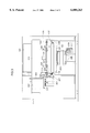
- the chuck 135 is closed and the edge portions of the protecting film 109 are grasped (FIG. 6E), the cutter 301 is moved along the Y axis (the direction from top to down in FIG. 2), and the protecting film 109 is cut.
- the cylinder 331 is simultaneously driven to also lower the side press roller 327 along the Y direction to move together with the cutter 301, whereby the protecting film 109 is pressed against the wafer W by the side press roller 327.
- the protecting film 109 undergoes double compression by the press rollers 107, 327 to be firmly applied to the wafer W.
- the press roller 107 and the chuck 135 are raised and remain on standby at the raised position until the next wafer comes. Further, the side press roller 327 is also raised.
- the table 201 is moved in the X direction (from the right to the left in FIG. 8B) only over the distance d X shown in FIG. 8B, while at the same time the cutting blade 301a is moved in the Y direction (the direction from bottom to top in FIG. 8B) only over the distance d Y . Further, in synchronization with the above-described movement, the table 201 is rotated only by an angular amount ⁇ in the counterclockwise direction shown in FIG. 8B about a center of rotation O.
Landscapes
- Engineering & Computer Science (AREA)
- Manufacturing & Machinery (AREA)
- Physics & Mathematics (AREA)
- Condensed Matter Physics & Semiconductors (AREA)
- General Physics & Mathematics (AREA)
- Computer Hardware Design (AREA)
- Microelectronics & Electronic Packaging (AREA)
- Power Engineering (AREA)
- Container, Conveyance, Adherence, Positioning, Of Wafer (AREA)
- Processing Of Stones Or Stones Resemblance Materials (AREA)
- Dicing (AREA)
Priority Applications (1)
| Application Number | Priority Date | Filing Date | Title |
|---|---|---|---|
| US09/481,998 US6258198B1 (en) | 1997-05-30 | 2000-01-11 | Method and apparatus for applying a protecting film to a semiconductor wafer |
Applications Claiming Priority (4)
| Application Number | Priority Date | Filing Date | Title |
|---|---|---|---|
| JP9-157831 | 1997-05-30 | ||
| JP15783197A JP3919292B2 (ja) | 1997-05-30 | 1997-05-30 | 半導体ウェハ保護フィルムの切断方法および装置 |
| JP15783097A JP3759820B2 (ja) | 1997-05-30 | 1997-05-30 | 半導体ウェハ保護フィルムの貼付方法および装置 |
| JP9-157830 | 1997-05-30 |
Related Child Applications (1)
| Application Number | Title | Priority Date | Filing Date |
|---|---|---|---|
| US09/481,998 Division US6258198B1 (en) | 1997-05-30 | 2000-01-11 | Method and apparatus for applying a protecting film to a semiconductor wafer |
Publications (1)
| Publication Number | Publication Date |
|---|---|
| US6080263A true US6080263A (en) | 2000-06-27 |
Family
ID=26485142
Family Applications (2)
| Application Number | Title | Priority Date | Filing Date |
|---|---|---|---|
| US09/073,156 Expired - Lifetime US6080263A (en) | 1997-05-30 | 1998-05-05 | Method and apparatus for applying a protecting film to a semiconductor wafer |
| US09/481,998 Expired - Fee Related US6258198B1 (en) | 1997-05-30 | 2000-01-11 | Method and apparatus for applying a protecting film to a semiconductor wafer |
Family Applications After (1)
| Application Number | Title | Priority Date | Filing Date |
|---|---|---|---|
| US09/481,998 Expired - Fee Related US6258198B1 (en) | 1997-05-30 | 2000-01-11 | Method and apparatus for applying a protecting film to a semiconductor wafer |
Country Status (7)
| Country | Link |
|---|---|
| US (2) | US6080263A (de) |
| EP (1) | EP0881663A3 (de) |
| KR (2) | KR100500066B1 (de) |
| CN (3) | CN1652298A (de) |
| MY (1) | MY123396A (de) |
| SG (2) | SG72813A1 (de) |
| TW (1) | TW385296B (de) |
Cited By (22)
| Publication number | Priority date | Publication date | Assignee | Title |
|---|---|---|---|---|
| US20020083810A1 (en) * | 2000-12-19 | 2002-07-04 | Peng Neo Chee | In-process tape bur monitoring |
| US6543510B1 (en) * | 2000-06-07 | 2003-04-08 | Micron Technology, Inc. | Apparatus and methods for coverlay removal and adhesive application |
| US6698488B2 (en) * | 2000-10-16 | 2004-03-02 | Oki Electric Industry Co., Ltd. | Apparatus for sticking a tape onto a semiconductor wafer and method of sticking the tape |
| US20040074607A1 (en) * | 2002-10-11 | 2004-04-22 | Lintec Corporation | Laminating apparatus |
| US6836166B2 (en) | 2003-01-08 | 2004-12-28 | Micron Technology, Inc. | Method and system for delay control in synchronization circuits |
| US6910403B1 (en) * | 1999-06-11 | 2005-06-28 | Tokyo Seimitsu Co., Ltd. | Method for cutting semiconductor wafer protecting sheet |
| US6962185B2 (en) * | 2001-12-26 | 2005-11-08 | Nec Electronics Corporation | Device for sticking protective sheet on substrate surface |
| US20060037694A1 (en) * | 2004-08-19 | 2006-02-23 | Nitto Denko Corporation | Method and apparatus for joining protective tape |
| US20060177954A1 (en) * | 2002-07-12 | 2006-08-10 | Samsung Electronics Co., Ltd. | Dicing tape attaching unit that can attach pre-cut dicing tape and general dicing tape to wafer and in-line system having the dicing tape attaching unit |
| US20060194412A1 (en) * | 2004-04-07 | 2006-08-31 | Takehito Nakayama | Method and device for sticking tape |
| US20070215638A1 (en) * | 2004-10-14 | 2007-09-20 | Glenn Roche | Flexible magnetised portion applicator dispensing apparatus and method |
| US20070227648A1 (en) * | 2004-04-28 | 2007-10-04 | Masaki Tsujimoto | Sticking Apparatus and Sticking Method |
| US20080011412A1 (en) * | 2004-06-25 | 2008-01-17 | Lintec Corporation | Sheet Peeling Apparatus and Peeling Method |
| US20080202692A1 (en) * | 2007-02-22 | 2008-08-28 | Masayuki Yamamoto | Adhesive tape joining apparatus |
| US20090120587A1 (en) * | 2005-07-07 | 2009-05-14 | Lintec Corporation | Sheet sticking table |
| CN101530972B (zh) * | 2008-03-11 | 2012-05-09 | 发那科株式会社 | 具备往复运动装置的加工机 |
| US8492176B2 (en) | 2011-10-11 | 2013-07-23 | Renesas Electronics Corporation | Method of manufacturing semiconductor device |
| US20140124126A1 (en) * | 2012-11-07 | 2014-05-08 | Samsung Display Co., Ltd. | Device and method for manufacturing donor substrate |
| US20150155195A1 (en) * | 2013-11-29 | 2015-06-04 | Taiwan Semiconductor Manufacturing Company, Ltd. | Wafer Taping Scheme |
| CN104795309A (zh) * | 2014-01-21 | 2015-07-22 | 东和株式会社 | 薄膜片材切除装置及切除方法 |
| US20220254664A1 (en) * | 2021-02-09 | 2022-08-11 | Disco Corporation | Sheet attaching apparatus |
| US20230009839A1 (en) * | 2021-07-09 | 2023-01-12 | Taiwan Semiconductor Manufacturing Company | System and method for chemical mechanical polishing pad replacement |
Families Citing this family (43)
| Publication number | Priority date | Publication date | Assignee | Title |
|---|---|---|---|---|
| US6080263A (en) * | 1997-05-30 | 2000-06-27 | Lintec Corporation | Method and apparatus for applying a protecting film to a semiconductor wafer |
| AT411856B (de) * | 2000-10-16 | 2004-06-25 | Datacon Semiconductor Equip | Verfahren zur herstellung einer klebeverbindung von einem scheibenförmigen halbleitersubstrat auf einen flexiblen adhäsiven transportträger sowie einrichtung zur durchführung dieses verfahrens |
| EP1249864A1 (de) * | 2001-04-09 | 2002-10-16 | ABB Schweiz AG | Verfahren und Gerät zum Reduzieren der Dicke von dünnen Scheiben |
| JP2002367931A (ja) * | 2001-06-07 | 2002-12-20 | Lintec Corp | ダイボンディングシート貼着装置およびダイボンディングシートの貼着方法 |
| JP2004047823A (ja) * | 2002-07-12 | 2004-02-12 | Tokyo Seimitsu Co Ltd | ダイシングテープ貼付装置およびバックグラインド・ダイシングテープ貼付システム |
| JP4330393B2 (ja) * | 2003-07-14 | 2009-09-16 | 日東電工株式会社 | 基板貼合せ方法およびその装置 |
| US6940181B2 (en) * | 2003-10-21 | 2005-09-06 | Micron Technology, Inc. | Thinned, strengthened semiconductor substrates and packages including same |
| US7064069B2 (en) * | 2003-10-21 | 2006-06-20 | Micron Technology, Inc. | Substrate thinning including planarization |
| JP2006272505A (ja) * | 2005-03-29 | 2006-10-12 | Nitto Denko Corp | 保護テープ切断方法およびこれを用いた装置 |
| CN100362623C (zh) * | 2005-12-08 | 2008-01-16 | 北京北方微电子基地设备工艺研究中心有限责任公司 | 一种硅片工艺试验方法 |
| KR100575559B1 (ko) * | 2005-12-27 | 2006-05-03 | 세호로보트산업 주식회사 | 커버레이 부착 시스템 |
| JP4360684B2 (ja) * | 2006-02-22 | 2009-11-11 | 日東電工株式会社 | 半導体ウエハの粘着テープ貼付け方法およびこれを用いた装置 |
| JP4884075B2 (ja) | 2006-05-22 | 2012-02-22 | 株式会社東京精密 | テープ貼付方法およびテープ貼付装置 |
| JP4642002B2 (ja) * | 2006-11-14 | 2011-03-02 | 日東電工株式会社 | 半導体ウエハの保護テープ切断方法および保護テープ切断装置 |
| JP4895766B2 (ja) * | 2006-11-14 | 2012-03-14 | 日東電工株式会社 | 半導体ウエハの保護テープ切断方法および保護テープ切断装置 |
| KR100822867B1 (ko) | 2007-03-15 | 2008-04-16 | 주식회사 퓨리텍 | 휴대용 롤와이퍼 커팅장치 |
| US8679694B2 (en) * | 2007-03-21 | 2014-03-25 | Societe Bic | Fluidic control system and method of manufacture |
| US8133629B2 (en) | 2007-03-21 | 2012-03-13 | SOCIéTé BIC | Fluidic distribution system and related methods |
| JP4865799B2 (ja) * | 2007-10-22 | 2012-02-01 | 株式会社アムクルー | 面発光体並びにこれを組み込んで成る内照式看板 |
| CN101197232B (zh) * | 2007-12-28 | 2010-10-13 | 南京华显高科有限公司 | 等离子体显示器中介质层的制作方法 |
| JP5160297B2 (ja) * | 2008-05-02 | 2013-03-13 | 日東電工株式会社 | カッタ刃の清掃方法およびカッタ刃の清掃装置、並びに、これを備えた粘着テープ貼付け装置 |
| CN102194654B (zh) * | 2010-03-03 | 2013-11-27 | 美商豪威科技股份有限公司 | 形成保护膜于微型摄像芯片上的装置及其形成方法 |
| US8932775B2 (en) | 2010-05-28 | 2015-01-13 | Toyota Jidosha Kabushiki Kaisha | Method and apparatus for controlling the operation of a fuel cell |
| US8571699B2 (en) * | 2010-09-10 | 2013-10-29 | Taiwan Semiconductor Manufacturing Company, Ltd. | System and method to reduce pre-back-grinding process defects |
| CN102082078B (zh) * | 2010-10-22 | 2012-10-03 | 上海技美电子科技有限公司 | 适于为超薄晶圆贴膜的贴膜方法及贴膜装置 |
| CN102120380B (zh) * | 2010-10-22 | 2013-11-06 | 上海技美电子科技有限公司 | 贴膜方法和贴膜装置 |
| CN102173316B (zh) * | 2010-12-21 | 2013-06-19 | 上海技美电子科技有限公司 | 贴膜方法及贴膜设备 |
| TWI451503B (zh) * | 2010-12-27 | 2014-09-01 | Omnivision Tech Inc | 形成保護膜於晶片封裝上之裝置及其形成方法 |
| CN102543768B (zh) * | 2010-12-30 | 2014-07-16 | 美商豪威科技股份有限公司 | 形成保护膜于芯片封装上的装置及其形成方法 |
| CN102623300B (zh) * | 2011-01-28 | 2014-08-20 | 美商豪威科技股份有限公司 | 形成保护膜于芯片级封装上的装置及其形成方法 |
| TWI458618B (zh) * | 2011-12-28 | 2014-11-01 | Mas Automation Corp | The cutting method and device of the soft side of the hard board |
| CN106217434B (zh) * | 2016-08-09 | 2017-12-26 | 歌尔股份有限公司 | 保护膜裁切工装 |
| CN106379593B (zh) * | 2016-09-08 | 2019-01-11 | 东莞市豪斯特热冲压技术有限公司 | 一种自动覆膜机 |
| JP6508161B2 (ja) | 2016-10-18 | 2019-05-08 | トヨタ自動車株式会社 | 燃料電池システム |
| JP6597566B2 (ja) | 2016-11-21 | 2019-10-30 | トヨタ自動車株式会社 | 燃料電池システム |
| JP7130401B2 (ja) * | 2018-03-29 | 2022-09-05 | 日東電工株式会社 | 粘着テープ貼付け方法および粘着テープ貼付け装置 |
| CN110449930A (zh) * | 2019-08-21 | 2019-11-15 | 重庆霖萌电子科技有限公司 | 一种数控雕刻机主轴动态施压系统 |
| CN110712362B (zh) * | 2019-09-24 | 2022-02-18 | 神通科技集团股份有限公司 | 一种自动贴膜设备及其贴膜方法 |
| CN110744733B (zh) * | 2019-09-25 | 2021-12-03 | 智科博芯(北京)科技有限公司 | 一种基于输送优化的plc内置八度角芯片的晶圆划片机 |
| TWI713134B (zh) * | 2019-11-14 | 2020-12-11 | 日月光半導體製造股份有限公司 | 用於製作半導體設備之整合系統 |
| JP7681414B2 (ja) * | 2021-03-25 | 2025-05-22 | 株式会社ディスコ | 保護シート貼着装置 |
| CN114783920B (zh) * | 2022-06-22 | 2022-09-06 | 四川明泰微电子有限公司 | 一种晶圆蓝膜张紧装置 |
| CN118472780B (zh) * | 2024-07-15 | 2024-11-15 | 长春中科长光时空光电技术有限公司 | 激光芯片加工装置 |
Citations (8)
| Publication number | Priority date | Publication date | Assignee | Title |
|---|---|---|---|---|
| JPS63250836A (ja) * | 1987-04-07 | 1988-10-18 | Nec Yamagata Ltd | ウエ−ハ表面保護テ−プ貼り付け装置 |
| US4865677A (en) * | 1987-08-11 | 1989-09-12 | Nitto Electric Industrial Co., Ltd. | Sticking and cutoff device for adhering adhesive tape on thin articles |
| US4925515A (en) * | 1987-11-27 | 1990-05-15 | Takatori Corporation | Method and apparatus for applying a protective tape on a wafer and cutting it out to shape |
| US5069738A (en) * | 1987-06-23 | 1991-12-03 | Kaysersberg Packaging, S.A. | Process and device for applying a protective film to an alveolated board |
| GB2256967A (en) * | 1991-06-17 | 1992-12-23 | Motorola Inc | Method of depositing a pecvd teos oxide film |
| US5228944A (en) * | 1990-02-15 | 1993-07-20 | Hoechst Aktiengesellschaft | Apparatus for producing composite bodies from layers of plastic flim laminated to one another |
| US5310442A (en) * | 1991-05-13 | 1994-05-10 | Nitto Denko Corporation | Apparatus for applying and removing protective adhesive tape to/from semiconductor wafer surfaces |
| JPH10300603A (ja) * | 1997-04-23 | 1998-11-13 | Denso Corp | 半導体式変位検出装置の製造方法 |
Family Cites Families (13)
| Publication number | Priority date | Publication date | Assignee | Title |
|---|---|---|---|---|
| DE1253860B (de) * | 1961-04-15 | 1967-11-09 | Vorwerk & Sohn | Spiralschnittmaschine zum Herstellen eines zur Verwendung als Schuhrahmen vorgesehenen Streifens |
| JPH0251249A (ja) * | 1988-08-15 | 1990-02-21 | Nitto Denko Corp | 半導体ウエハの自動貼付け装置 |
| US5106450A (en) * | 1990-12-20 | 1992-04-21 | International Business Machines Corporation | Dry film resist transport and lamination system for semiconductor wafers |
| JPH0536657A (ja) * | 1991-07-29 | 1993-02-12 | Nitto Denko Corp | 半導体ウエハの保護テープ切抜き装置 |
| KR960016505B1 (ko) * | 1993-08-07 | 1996-12-12 | 엘지반도체 주식회사 | 진공챔버를 이용한 웨이퍼 마운팅 방법 및 그 장치 |
| KR970002433B1 (ko) * | 1993-12-31 | 1997-03-05 | 삼성전자 주식회사 | 마스킹 필름의 부착 방법 및 이에 사용되는 마스킹 필름 부착 장치 |
| US5590445A (en) * | 1994-03-22 | 1997-01-07 | Teikoku Seiki Kabushiki Kaisha | Tape extension device for semiconductor producing apparatus and semiconductor producing apparatus with tape extension device |
| KR0143386B1 (ko) * | 1994-09-06 | 1998-07-15 | 한동근 | 네일 염착제 조성물 |
| JPH10112492A (ja) * | 1996-10-07 | 1998-04-28 | Teikoku Seiki Kk | ウェハ保護テープの裁断方法及びその装置 |
| JP3759820B2 (ja) * | 1997-05-30 | 2006-03-29 | リンテック株式会社 | 半導体ウェハ保護フィルムの貼付方法および装置 |
| US6080263A (en) * | 1997-05-30 | 2000-06-27 | Lintec Corporation | Method and apparatus for applying a protecting film to a semiconductor wafer |
| JP3919292B2 (ja) * | 1997-05-30 | 2007-05-23 | リンテック株式会社 | 半導体ウェハ保護フィルムの切断方法および装置 |
| KR100954956B1 (ko) * | 2007-12-28 | 2010-04-27 | 장수관 | 탄성 포장재 및 이를 이용한 탄성 포장막의 형성방법 |
-
1998
- 1998-05-05 US US09/073,156 patent/US6080263A/en not_active Expired - Lifetime
- 1998-05-11 EP EP98108540A patent/EP0881663A3/de not_active Withdrawn
- 1998-05-14 TW TW087107433A patent/TW385296B/zh not_active IP Right Cessation
- 1998-05-14 SG SG1998001040A patent/SG72813A1/en unknown
- 1998-05-14 SG SG200000160A patent/SG102564A1/en unknown
- 1998-05-21 MY MYPI98002256A patent/MY123396A/en unknown
- 1998-05-29 KR KR1019980019729A patent/KR100500066B1/ko not_active Expired - Fee Related
- 1998-05-29 CN CNA2005100525725A patent/CN1652298A/zh active Pending
- 1998-05-29 CN CNB981093620A patent/CN1146016C/zh not_active Expired - Fee Related
- 1998-05-29 CN CNB03107748XA patent/CN1254847C/zh not_active Expired - Fee Related
-
2000
- 2000-01-11 US US09/481,998 patent/US6258198B1/en not_active Expired - Fee Related
-
2005
- 2005-03-07 KR KR1020050018483A patent/KR100500626B1/ko not_active Expired - Fee Related
Patent Citations (8)
| Publication number | Priority date | Publication date | Assignee | Title |
|---|---|---|---|---|
| JPS63250836A (ja) * | 1987-04-07 | 1988-10-18 | Nec Yamagata Ltd | ウエ−ハ表面保護テ−プ貼り付け装置 |
| US5069738A (en) * | 1987-06-23 | 1991-12-03 | Kaysersberg Packaging, S.A. | Process and device for applying a protective film to an alveolated board |
| US4865677A (en) * | 1987-08-11 | 1989-09-12 | Nitto Electric Industrial Co., Ltd. | Sticking and cutoff device for adhering adhesive tape on thin articles |
| US4925515A (en) * | 1987-11-27 | 1990-05-15 | Takatori Corporation | Method and apparatus for applying a protective tape on a wafer and cutting it out to shape |
| US5228944A (en) * | 1990-02-15 | 1993-07-20 | Hoechst Aktiengesellschaft | Apparatus for producing composite bodies from layers of plastic flim laminated to one another |
| US5310442A (en) * | 1991-05-13 | 1994-05-10 | Nitto Denko Corporation | Apparatus for applying and removing protective adhesive tape to/from semiconductor wafer surfaces |
| GB2256967A (en) * | 1991-06-17 | 1992-12-23 | Motorola Inc | Method of depositing a pecvd teos oxide film |
| JPH10300603A (ja) * | 1997-04-23 | 1998-11-13 | Denso Corp | 半導体式変位検出装置の製造方法 |
Cited By (37)
| Publication number | Priority date | Publication date | Assignee | Title |
|---|---|---|---|---|
| US6910403B1 (en) * | 1999-06-11 | 2005-06-28 | Tokyo Seimitsu Co., Ltd. | Method for cutting semiconductor wafer protecting sheet |
| US6543510B1 (en) * | 2000-06-07 | 2003-04-08 | Micron Technology, Inc. | Apparatus and methods for coverlay removal and adhesive application |
| US6749711B2 (en) | 2000-06-07 | 2004-06-15 | Micron Technology, Inc. | Apparatus and methods for coverlay removal and adhesive application |
| US20050034818A1 (en) * | 2000-06-07 | 2005-02-17 | Micron Technology, Inc. | Apparatus and methods for coverlay removal and adhesive application |
| US6698488B2 (en) * | 2000-10-16 | 2004-03-02 | Oki Electric Industry Co., Ltd. | Apparatus for sticking a tape onto a semiconductor wafer and method of sticking the tape |
| US20030209117A1 (en) * | 2000-12-19 | 2003-11-13 | Peng Neo Chee | In-process tape bur monitoring |
| US20020083810A1 (en) * | 2000-12-19 | 2002-07-04 | Peng Neo Chee | In-process tape bur monitoring |
| US7004054B2 (en) | 2000-12-19 | 2006-02-28 | Micron Technology, Inc. | In-process tape bur monitoring |
| US6845695B2 (en) | 2000-12-19 | 2005-01-25 | Micron Technology, Inc. | In-process tape bur monitoring |
| US6962185B2 (en) * | 2001-12-26 | 2005-11-08 | Nec Electronics Corporation | Device for sticking protective sheet on substrate surface |
| US20060177954A1 (en) * | 2002-07-12 | 2006-08-10 | Samsung Electronics Co., Ltd. | Dicing tape attaching unit that can attach pre-cut dicing tape and general dicing tape to wafer and in-line system having the dicing tape attaching unit |
| US20040074607A1 (en) * | 2002-10-11 | 2004-04-22 | Lintec Corporation | Laminating apparatus |
| US6836166B2 (en) | 2003-01-08 | 2004-12-28 | Micron Technology, Inc. | Method and system for delay control in synchronization circuits |
| US20100276074A1 (en) * | 2003-04-09 | 2010-11-04 | Lintec Corporation | Method for Sticking Tape |
| US20060194412A1 (en) * | 2004-04-07 | 2006-08-31 | Takehito Nakayama | Method and device for sticking tape |
| US20070227648A1 (en) * | 2004-04-28 | 2007-10-04 | Masaki Tsujimoto | Sticking Apparatus and Sticking Method |
| US7611600B2 (en) * | 2004-04-28 | 2009-11-03 | Lintec Corporation | Sticking apparatus and sticking method |
| US20080011412A1 (en) * | 2004-06-25 | 2008-01-17 | Lintec Corporation | Sheet Peeling Apparatus and Peeling Method |
| US20060037694A1 (en) * | 2004-08-19 | 2006-02-23 | Nitto Denko Corporation | Method and apparatus for joining protective tape |
| US7516768B2 (en) * | 2004-08-19 | 2009-04-14 | Nitto Denko Corporation | Method and apparatus for joining protective tape |
| US20070215638A1 (en) * | 2004-10-14 | 2007-09-20 | Glenn Roche | Flexible magnetised portion applicator dispensing apparatus and method |
| US7984740B2 (en) * | 2004-10-14 | 2011-07-26 | Glenn Roche | Flexible magnetised portion applicator dispensing apparatus and method |
| US20090120587A1 (en) * | 2005-07-07 | 2009-05-14 | Lintec Corporation | Sheet sticking table |
| US20080202692A1 (en) * | 2007-02-22 | 2008-08-28 | Masayuki Yamamoto | Adhesive tape joining apparatus |
| US7661454B2 (en) * | 2007-02-22 | 2010-02-16 | Nitto Denko Corporation | Adhesive tape joining apparatus |
| CN101530972B (zh) * | 2008-03-11 | 2012-05-09 | 发那科株式会社 | 具备往复运动装置的加工机 |
| US8492176B2 (en) | 2011-10-11 | 2013-07-23 | Renesas Electronics Corporation | Method of manufacturing semiconductor device |
| US20140124126A1 (en) * | 2012-11-07 | 2014-05-08 | Samsung Display Co., Ltd. | Device and method for manufacturing donor substrate |
| US9748130B2 (en) * | 2013-11-29 | 2017-08-29 | Taiwan Semiconductor Manufacturing Company, Ltd. | Wafer taping scheme |
| US20150155195A1 (en) * | 2013-11-29 | 2015-06-04 | Taiwan Semiconductor Manufacturing Company, Ltd. | Wafer Taping Scheme |
| CN104795309A (zh) * | 2014-01-21 | 2015-07-22 | 东和株式会社 | 薄膜片材切除装置及切除方法 |
| CN104795309B (zh) * | 2014-01-21 | 2018-06-01 | 东和株式会社 | 薄膜片材切除装置及切除方法 |
| US20220254664A1 (en) * | 2021-02-09 | 2022-08-11 | Disco Corporation | Sheet attaching apparatus |
| KR20220115056A (ko) * | 2021-02-09 | 2022-08-17 | 가부시기가이샤 디스코 | 시트 첩착 장치 |
| US11942339B2 (en) * | 2021-02-09 | 2024-03-26 | Disco Corporation | Sheet attaching apparatus |
| US20230009839A1 (en) * | 2021-07-09 | 2023-01-12 | Taiwan Semiconductor Manufacturing Company | System and method for chemical mechanical polishing pad replacement |
| US12202094B2 (en) * | 2021-07-09 | 2025-01-21 | Taiwan Semiconductor Manufacturing Company, Ltd. | System and method for chemical mechanical polishing pad replacement |
Also Published As
| Publication number | Publication date |
|---|---|
| TW385296B (en) | 2000-03-21 |
| US6258198B1 (en) | 2001-07-10 |
| KR100500066B1 (ko) | 2006-07-25 |
| CN1515464A (zh) | 2004-07-28 |
| EP0881663A2 (de) | 1998-12-02 |
| EP0881663A3 (de) | 2003-12-17 |
| SG72813A1 (en) | 2000-05-23 |
| KR19980087499A (ko) | 1998-12-05 |
| CN1208946A (zh) | 1999-02-24 |
| CN1254847C (zh) | 2006-05-03 |
| KR100500626B1 (ko) | 2005-07-12 |
| MY123396A (en) | 2006-05-31 |
| CN1652298A (zh) | 2005-08-10 |
| CN1146016C (zh) | 2004-04-14 |
| SG102564A1 (en) | 2004-03-26 |
Similar Documents
| Publication | Publication Date | Title |
|---|---|---|
| US6080263A (en) | Method and apparatus for applying a protecting film to a semiconductor wafer | |
| KR100652257B1 (ko) | 이면 연삭/다이싱 테이프 부착 시스템 | |
| US6616799B2 (en) | Sheet removing apparatus and method | |
| CN101181834B (zh) | 半导体晶圆的保护带切断方法及保护带切断装置 | |
| JPH0583170B2 (de) | ||
| JP3759820B2 (ja) | 半導体ウェハ保護フィルムの貼付方法および装置 | |
| TW201112319A (en) | Adhesive tape joining method and adhesive tape joining apparatus | |
| JP4371890B2 (ja) | 貼付装置及び貼付方法 | |
| US20080044258A1 (en) | Fragile Member Processing System | |
| JP3545758B2 (ja) | 半導体ウェハ保護フィルムの切断方法および装置 | |
| CN109637948B (zh) | 扩展方法和扩展装置 | |
| EP1614649B1 (de) | Verfahren und vorrichtung zum kleben von bändern | |
| JP3919292B2 (ja) | 半導体ウェハ保護フィルムの切断方法および装置 | |
| US7900677B2 (en) | Sheet sticking apparatus | |
| JP2006187862A (ja) | 切断装置及び切断方法 | |
| US20100276074A1 (en) | Method for Sticking Tape | |
| JP4326363B2 (ja) | 粘着シート貼付け方法およびこれを用いた装置 | |
| JP5554100B2 (ja) | シート切断方法およびシート切断装置 | |
| JP2003338477A (ja) | テープ剥離方法 | |
| JPH04340746A (ja) | 粘着テープの貼着装置 | |
| JP2005136307A (ja) | 貼合装置 | |
| JP2005297458A (ja) | 貼付装置 | |
| JP2004128020A (ja) | 保護テープの剥離装置および保護テープの剥離方法 | |
| CN115838093A (zh) | 带粘贴装置 | |
| JP2025159937A (ja) | 保持装置および保持方法 |
Legal Events
| Date | Code | Title | Description |
|---|---|---|---|
| AS | Assignment |
Owner name: LINTEC CORPORATION, JAPAN Free format text: ASSIGNMENT OF ASSIGNORS INTEREST;ASSIGNORS:SATO, HIROSHI;KURITA, TSUYOSHI;OKAMOTO, KOJI;REEL/FRAME:009158/0765 Effective date: 19980422 |
|
| FEPP | Fee payment procedure |
Free format text: PAYOR NUMBER ASSIGNED (ORIGINAL EVENT CODE: ASPN); ENTITY STATUS OF PATENT OWNER: LARGE ENTITY |
|
| STCF | Information on status: patent grant |
Free format text: PATENTED CASE |
|
| FPAY | Fee payment |
Year of fee payment: 4 |
|
| FPAY | Fee payment |
Year of fee payment: 8 |
|
| FPAY | Fee payment |
Year of fee payment: 12 |