JP4642002B2 - 半導体ウエハの保護テープ切断方法および保護テープ切断装置 - Google Patents
半導体ウエハの保護テープ切断方法および保護テープ切断装置 Download PDFInfo
- Publication number
- JP4642002B2 JP4642002B2 JP2006307726A JP2006307726A JP4642002B2 JP 4642002 B2 JP4642002 B2 JP 4642002B2 JP 2006307726 A JP2006307726 A JP 2006307726A JP 2006307726 A JP2006307726 A JP 2006307726A JP 4642002 B2 JP4642002 B2 JP 4642002B2
- Authority
- JP
- Japan
- Prior art keywords
- cutter blade
- semiconductor wafer
- protective tape
- wafer
- force
- Prior art date
- Legal status (The legal status is an assumption and is not a legal conclusion. Google has not performed a legal analysis and makes no representation as to the accuracy of the status listed.)
- Expired - Fee Related
Links
Images


Classifications
-
- B—PERFORMING OPERATIONS; TRANSPORTING
- B26—HAND CUTTING TOOLS; CUTTING; SEVERING
- B26F—PERFORATING; PUNCHING; CUTTING-OUT; STAMPING-OUT; SEVERING BY MEANS OTHER THAN CUTTING
- B26F1/00—Perforating; Punching; Cutting-out; Stamping-out; Apparatus therefor
- B26F1/38—Cutting-out; Stamping-out
- B26F1/3846—Cutting-out; Stamping-out cutting out discs or the like
-
- H—ELECTRICITY
- H10—SEMICONDUCTOR DEVICES; ELECTRIC SOLID-STATE DEVICES NOT OTHERWISE PROVIDED FOR
- H10W—GENERIC PACKAGES, INTERCONNECTIONS, CONNECTORS OR OTHER CONSTRUCTIONAL DETAILS OF DEVICES COVERED BY CLASS H10
- H10W99/00—Subject matter not provided for in other groups of this subclass
-
- H—ELECTRICITY
- H10—SEMICONDUCTOR DEVICES; ELECTRIC SOLID-STATE DEVICES NOT OTHERWISE PROVIDED FOR
- H10P—GENERIC PROCESSES OR APPARATUS FOR THE MANUFACTURE OR TREATMENT OF DEVICES COVERED BY CLASS H10
- H10P72/00—Handling or holding of wafers, substrates or devices during manufacture or treatment thereof
- H10P72/04—Apparatus for manufacture or treatment
- H10P72/0442—Apparatus for placing on an insulating substrate, e.g. tape
-
- Y—GENERAL TAGGING OF NEW TECHNOLOGICAL DEVELOPMENTS; GENERAL TAGGING OF CROSS-SECTIONAL TECHNOLOGIES SPANNING OVER SEVERAL SECTIONS OF THE IPC; TECHNICAL SUBJECTS COVERED BY FORMER USPC CROSS-REFERENCE ART COLLECTIONS [XRACs] AND DIGESTS
- Y10—TECHNICAL SUBJECTS COVERED BY FORMER USPC
- Y10T—TECHNICAL SUBJECTS COVERED BY FORMER US CLASSIFICATION
- Y10T83/00—Cutting
- Y10T83/141—With means to monitor and control operation [e.g., self-regulating means]
-
- Y—GENERAL TAGGING OF NEW TECHNOLOGICAL DEVELOPMENTS; GENERAL TAGGING OF CROSS-SECTIONAL TECHNOLOGIES SPANNING OVER SEVERAL SECTIONS OF THE IPC; TECHNICAL SUBJECTS COVERED BY FORMER USPC CROSS-REFERENCE ART COLLECTIONS [XRACs] AND DIGESTS
- Y10—TECHNICAL SUBJECTS COVERED BY FORMER USPC
- Y10T—TECHNICAL SUBJECTS COVERED BY FORMER US CLASSIFICATION
- Y10T83/00—Cutting
- Y10T83/162—With control means responsive to replaceable or selectable information program
- Y10T83/173—Arithmetically determined program
-
- Y—GENERAL TAGGING OF NEW TECHNOLOGICAL DEVELOPMENTS; GENERAL TAGGING OF CROSS-SECTIONAL TECHNOLOGIES SPANNING OVER SEVERAL SECTIONS OF THE IPC; TECHNICAL SUBJECTS COVERED BY FORMER USPC CROSS-REFERENCE ART COLLECTIONS [XRACs] AND DIGESTS
- Y10—TECHNICAL SUBJECTS COVERED BY FORMER USPC
- Y10T—TECHNICAL SUBJECTS COVERED BY FORMER US CLASSIFICATION
- Y10T83/00—Cutting
- Y10T83/869—Means to drive or to guide tool
- Y10T83/8776—Constantly urged tool or tool support [e.g., spring biased]
Landscapes
- Life Sciences & Earth Sciences (AREA)
- Forests & Forestry (AREA)
- Engineering & Computer Science (AREA)
- Mechanical Engineering (AREA)
- Container, Conveyance, Adherence, Positioning, Of Wafer (AREA)
- Processing Of Stones Or Stones Resemblance Materials (AREA)
Description
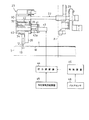
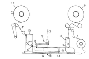
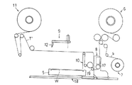
ウエハ径方向に移動可能に支持した前記カッタ刃を半導体ウエハの外周縁に押し付け付勢するとともに、この押し付け付勢力をカッタ刃の走行速度変動に対応させて自動調整制御し、半導体ウエハの外周縁に対するカッタ刃の接触圧力を安定維持する
ことを特徴とする。
前記カッタ刃にウエハの外周縁に向かう一定の押し付け付勢力を付与するとともに、この押し付け付勢力より小さい制御用の押し戻し力を逆方向から付与し、この押し戻し力をカッタ刃の走行速度変動に対応させて自動調整制御する
ことを特徴とする。
ウエハ径方向に移動可能に支持した前記カッタ刃に半導体ウエハの外周縁に向かう一定の押し付け付勢力を付与する押し付け付勢手段と、
前記押し付け付勢力より小さい押し戻し力を押し付け付勢方向と逆方向にカッタ刃に付与する押し戻し手段と、
この押し戻し手段による押し戻し力をカッタ刃の走行速度変動に対応させて自動調整制御する制御手段と、
を備えてあることを特徴とする。
前記押し付け付勢手段は、バネの弾性復元力で前記カッタ刃を半導体ウエハの外周縁に向けて押し付け付勢するよう構成したものであり、
前記押し戻し手段は、エアーシリンダでカッタ刃を押し付け付勢方向と逆方向に押圧するよう構成したものであり、
前記制御手段は、前記エアーシリンダに供給される空気圧をカッタ刃の走行速度変動に対応させて自動調整制御するよう構成した
ことを特徴とする。
42 … バネ
43 … エアーシリンダ
T … 保護テープ
c … 接触圧力
F … 押し付け付勢力
h … 押し戻し力
g … 遠心力
P … 空気圧
W … 半導体ウエハ
Claims (4)
- 半導体ウエハの外周縁に沿ってカッタ刃を旋回走行させて、半導体ウエハの表面に貼り付けられた保護テープをウエハ外形に沿って切り抜く半導体ウエハの保護テープ切断方法であって、
ウエハ径方向に移動可能に支持した前記カッタ刃を半導体ウエハの外周縁に押し付け付勢するとともに、この押し付け付勢力をカッタ刃の走行速度変動に対応させて自動調整制御し、半導体ウエハの外周縁に対するカッタ刃の接触圧力を安定維持する
ことを特徴とする半導体ウエハの保護テープ切断方法。 - 請求項1に記載の半導体ウエハの保護テープ切断方法において、
前記カッタ刃にウエハの外周縁に向かう一定の押し付け付勢力を付与するとともに、この押し付け付勢力より小さい制御用の押し戻し力を逆方向から付与し、この押し戻し力をカッタ刃の走行速度変動に対応させて自動調整制御する
ことを特徴とする半導体ウエハの保護テープ切断方法。 - 半導体ウエハの外周縁に沿ってカッタ刃を旋回走行させて、半導体ウエハの表面に貼り付けられた保護テープをウエハ外形に沿って切り抜く半導体ウエハの保護テープ切断装置であって、
ウエハ径方向に移動可能に支持した前記カッタ刃に半導体ウエハの外周縁に向かう一定の押し付け付勢力を付与する押し付け付勢手段と、
前記押し付け付勢力より小さい押し戻し力を押し付け付勢方向と逆方向にカッタ刃に付与する押し戻し手段と、
この押し戻し手段による押し戻し力をカッタ刃の走行速度変動に対応させて自動調整制御する制御手段と、
を備えたことを特徴とする半導体ウエハの保護テープ切断装置。 - 請求項3に記載の半導体ウエハの保護テープ切断装置において、
前記押し付け付勢手段は、バネの弾性復元力で前記カッタ刃を半導体ウエハの外周縁に向けて押し付け付勢するよう構成したものであり、
前記押し戻し手段は、エアーシリンダでカッタ刃を押し付け付勢方向と逆方向に押圧するよう構成したものであり、
前記制御手段は、前記エアーシリンダに供給される空気圧をカッタ刃の走行速度変動に対応させて自動調整制御するよう構成した
ことを特徴とする半導体ウエハの保護テープ切断装置。
Priority Applications (5)
| Application Number | Priority Date | Filing Date | Title |
|---|---|---|---|
| JP2006307726A JP4642002B2 (ja) | 2006-11-14 | 2006-11-14 | 半導体ウエハの保護テープ切断方法および保護テープ切断装置 |
| US11/979,932 US8042441B2 (en) | 2006-11-14 | 2007-11-09 | Method for cutting protective tape of semiconductor wafer and apparatus for cutting the protective tape |
| KR1020070115307A KR101311567B1 (ko) | 2006-11-14 | 2007-11-13 | 반도체 웨이퍼의 보호 테이프 절단 방법 및 보호 테이프절단 장치 |
| TW096142774A TWI368269B (en) | 2006-11-14 | 2007-11-13 | Method for cutting protective tape of semiconductor wafer and apparatus for cutting the protective tape |
| CN2007101878687A CN101183641B (zh) | 2006-11-14 | 2007-11-14 | 半导体晶圆的保护带切断方法及保护带切断装置 |
Applications Claiming Priority (1)
| Application Number | Priority Date | Filing Date | Title |
|---|---|---|---|
| JP2006307726A JP4642002B2 (ja) | 2006-11-14 | 2006-11-14 | 半導体ウエハの保護テープ切断方法および保護テープ切断装置 |
Publications (2)
| Publication Number | Publication Date |
|---|---|
| JP2008124307A JP2008124307A (ja) | 2008-05-29 |
| JP4642002B2 true JP4642002B2 (ja) | 2011-03-02 |
Family
ID=39369694
Family Applications (1)
| Application Number | Title | Priority Date | Filing Date |
|---|---|---|---|
| JP2006307726A Expired - Fee Related JP4642002B2 (ja) | 2006-11-14 | 2006-11-14 | 半導体ウエハの保護テープ切断方法および保護テープ切断装置 |
Country Status (5)
| Country | Link |
|---|---|
| US (1) | US8042441B2 (ja) |
| JP (1) | JP4642002B2 (ja) |
| KR (1) | KR101311567B1 (ja) |
| CN (1) | CN101183641B (ja) |
| TW (1) | TWI368269B (ja) |
Families Citing this family (9)
| Publication number | Priority date | Publication date | Assignee | Title |
|---|---|---|---|---|
| JP5412260B2 (ja) * | 2009-12-10 | 2014-02-12 | 日東電工株式会社 | 粘着テープ貼付け方法およびこれを用いた装置 |
| KR101981639B1 (ko) * | 2012-11-13 | 2019-05-27 | 삼성디스플레이 주식회사 | 시트 커팅 장치 및 그것을 이용한 시트 커팅 방법 |
| JP6122311B2 (ja) * | 2013-02-28 | 2017-04-26 | 日東電工株式会社 | 粘着テープ切断方法および粘着テープ片切断装置 |
| JP7360812B2 (ja) * | 2019-05-17 | 2023-10-13 | リンテック株式会社 | シート支持装置およびシート支持方法 |
| JP7273614B2 (ja) * | 2019-05-17 | 2023-05-15 | リンテック株式会社 | シート支持装置およびシート支持方法 |
| WO2022107192A1 (ja) * | 2020-11-17 | 2022-05-27 | スターテクノ株式会社 | ワーク加工装置及びそのワーク加工装置を備えた超音波加工装置 |
| CN112318691A (zh) * | 2020-12-04 | 2021-02-05 | 禹州市国粹钧窑有限责任公司 | 一种钧瓷瓶口加工方法及装置 |
| CN114030094B (zh) * | 2021-11-18 | 2022-12-09 | 江苏纳沛斯半导体有限公司 | 一种可防止产生崩边的半导体晶圆制备的硅片划片系统 |
| WO2024191582A1 (en) * | 2023-03-15 | 2024-09-19 | Applied Materials, Inc. | Method of laminating an interposer for die transfer substrates |
Family Cites Families (12)
| Publication number | Priority date | Publication date | Assignee | Title |
|---|---|---|---|---|
| US4603609A (en) * | 1983-10-21 | 1986-08-05 | Disco Abrasive Systems, Ltd. | Apparatus for cutting a sheet-like member applied to a surface of a semiconductor wafer |
| US4626320A (en) * | 1984-02-22 | 1986-12-02 | Conoco Inc. | Method for automated de-coking |
| JPH01143211A (ja) * | 1987-11-27 | 1989-06-05 | Takatori Haitetsuku:Kk | ウエハーに対する保護テープの貼付け切り抜き方法および装置 |
| JPH10112492A (ja) * | 1996-10-07 | 1998-04-28 | Teikoku Seiki Kk | ウェハ保護テープの裁断方法及びその装置 |
| JP3919292B2 (ja) * | 1997-05-30 | 2007-05-23 | リンテック株式会社 | 半導体ウェハ保護フィルムの切断方法および装置 |
| US6080263A (en) * | 1997-05-30 | 2000-06-27 | Lintec Corporation | Method and apparatus for applying a protecting film to a semiconductor wafer |
| JP3983053B2 (ja) * | 2002-01-17 | 2007-09-26 | 日東電工株式会社 | 保護テープの切断方法およびそれを用いた保護テープ貼付装置 |
| JP2004025402A (ja) | 2002-06-27 | 2004-01-29 | Lintec Corp | 半導体ウェハの保護テープの切断方法および切断装置 |
| JP4530638B2 (ja) * | 2003-10-07 | 2010-08-25 | 日東電工株式会社 | 半導体ウエハへの保護テープ貼付方法及び貼付装置 |
| JP4472316B2 (ja) | 2003-11-28 | 2010-06-02 | 日東電工株式会社 | 粘着テープ切断方法及び粘着テープ切断装置 |
| JP4387879B2 (ja) * | 2004-06-17 | 2009-12-24 | 株式会社ディスコ | 保護テープ装着方法および保護テープ装着装置 |
| JP4450696B2 (ja) * | 2004-08-19 | 2010-04-14 | 日東電工株式会社 | 保護テープ貼付け装置 |
-
2006
- 2006-11-14 JP JP2006307726A patent/JP4642002B2/ja not_active Expired - Fee Related
-
2007
- 2007-11-09 US US11/979,932 patent/US8042441B2/en not_active Expired - Fee Related
- 2007-11-13 TW TW096142774A patent/TWI368269B/zh not_active IP Right Cessation
- 2007-11-13 KR KR1020070115307A patent/KR101311567B1/ko not_active Expired - Fee Related
- 2007-11-14 CN CN2007101878687A patent/CN101183641B/zh not_active Expired - Fee Related
Also Published As
| Publication number | Publication date |
|---|---|
| US8042441B2 (en) | 2011-10-25 |
| KR20080043718A (ko) | 2008-05-19 |
| US20080113492A1 (en) | 2008-05-15 |
| CN101183641B (zh) | 2011-04-20 |
| CN101183641A (zh) | 2008-05-21 |
| TW200834700A (en) | 2008-08-16 |
| JP2008124307A (ja) | 2008-05-29 |
| KR101311567B1 (ko) | 2013-09-26 |
| TWI368269B (en) | 2012-07-11 |
Similar Documents
| Publication | Publication Date | Title |
|---|---|---|
| KR101311567B1 (ko) | 반도체 웨이퍼의 보호 테이프 절단 방법 및 보호 테이프절단 장치 | |
| US7850799B2 (en) | Method for affixing adhesive tape to semiconductor wafer, and apparatus using the same | |
| CN1738005B (zh) | 贴附保护带的方法和设备 | |
| US7896050B2 (en) | Apparatus for cutting the protective tape of semiconductor wafer | |
| US7357165B2 (en) | Method and apparatus for cutting protective tape | |
| US8021509B2 (en) | Method for affixing adhesive tape to semiconductor wafer, and apparatus using the same | |
| EP1962324B1 (en) | Adhesive tape joining apparatus | |
| JP5324317B2 (ja) | 保護テープ貼付け方法および保護テープ貼付け装置 | |
| US7789121B2 (en) | Sheet sticking apparatus and sticking method | |
| JP4326363B2 (ja) | 粘着シート貼付け方法およびこれを用いた装置 | |
| JP4640763B2 (ja) | 半導体ウエハの保護テープ切断方法および保護テープ切断装置 | |
| JP2013230532A (ja) | 半導体ウエハの保護テープ切断方法および保護テープ切断装置 | |
| JP5159566B2 (ja) | シート剥離装置および剥離方法 | |
| JP2580276B2 (ja) | 巻線用テ―ピング装置 | |
| JP3129468B2 (ja) | ワイヤ放電加工機 | |
| JP2002018603A (ja) | 棒材供給機 | |
| JPH08318526A (ja) | スライシングマシンのウェーハ回収装置 |
Legal Events
| Date | Code | Title | Description |
|---|---|---|---|
| A621 | Written request for application examination |
Free format text: JAPANESE INTERMEDIATE CODE: A621 Effective date: 20090219 |
|
| A977 | Report on retrieval |
Free format text: JAPANESE INTERMEDIATE CODE: A971007 Effective date: 20101126 |
|
| TRDD | Decision of grant or rejection written | ||
| A01 | Written decision to grant a patent or to grant a registration (utility model) |
Free format text: JAPANESE INTERMEDIATE CODE: A01 Effective date: 20101130 |
|
| A01 | Written decision to grant a patent or to grant a registration (utility model) |
Free format text: JAPANESE INTERMEDIATE CODE: A01 |
|
| A61 | First payment of annual fees (during grant procedure) |
Free format text: JAPANESE INTERMEDIATE CODE: A61 Effective date: 20101130 |
|
| R150 | Certificate of patent or registration of utility model |
Ref document number: 4642002 Country of ref document: JP Free format text: JAPANESE INTERMEDIATE CODE: R150 Free format text: JAPANESE INTERMEDIATE CODE: R150 |
|
| FPAY | Renewal fee payment (event date is renewal date of database) |
Free format text: PAYMENT UNTIL: 20131210 Year of fee payment: 3 |
|
| FPAY | Renewal fee payment (event date is renewal date of database) |
Free format text: PAYMENT UNTIL: 20131210 Year of fee payment: 3 |
|
| FPAY | Renewal fee payment (event date is renewal date of database) |
Free format text: PAYMENT UNTIL: 20161210 Year of fee payment: 6 |
|
| R250 | Receipt of annual fees |
Free format text: JAPANESE INTERMEDIATE CODE: R250 |
|
| R250 | Receipt of annual fees |
Free format text: JAPANESE INTERMEDIATE CODE: R250 |
|
| LAPS | Cancellation because of no payment of annual fees |