US5597469A - Process for selective application of solder to circuit packages - Google Patents
Process for selective application of solder to circuit packages Download PDFInfo
- Publication number
- US5597469A US5597469A US08/387,686 US38768695A US5597469A US 5597469 A US5597469 A US 5597469A US 38768695 A US38768695 A US 38768695A US 5597469 A US5597469 A US 5597469A
- Authority
- US
- United States
- Prior art keywords
- solder
- layer
- copper
- apertures
- electroplating
- Prior art date
- Legal status (The legal status is an assumption and is not a legal conclusion. Google has not performed a legal analysis and makes no representation as to the accuracy of the status listed.)
- Expired - Fee Related
Links
- 229910000679 solder Inorganic materials 0.000 title claims abstract description 181
- 238000000034 method Methods 0.000 title claims description 68
- 230000008569 process Effects 0.000 title description 38
- 239000000463 material Substances 0.000 claims abstract description 100
- 239000004020 conductor Substances 0.000 claims abstract description 28
- 238000009713 electroplating Methods 0.000 claims abstract description 26
- 239000012530 fluid Substances 0.000 claims abstract description 19
- 238000013019 agitation Methods 0.000 abstract description 13
- 238000000151 deposition Methods 0.000 abstract description 13
- 239000000470 constituent Substances 0.000 abstract description 8
- 238000007654 immersion Methods 0.000 abstract description 4
- 238000005530 etching Methods 0.000 abstract description 2
- 230000000873 masking effect Effects 0.000 abstract 1
- 239000010410 layer Substances 0.000 description 88
- RYGMFSIKBFXOCR-UHFFFAOYSA-N Copper Chemical compound [Cu] RYGMFSIKBFXOCR-UHFFFAOYSA-N 0.000 description 56
- 229910052802 copper Inorganic materials 0.000 description 56
- 239000010949 copper Substances 0.000 description 56
- 229910052751 metal Inorganic materials 0.000 description 20
- 239000002184 metal Substances 0.000 description 20
- 238000007747 plating Methods 0.000 description 20
- ATJFFYVFTNAWJD-UHFFFAOYSA-N Tin Chemical compound [Sn] ATJFFYVFTNAWJD-UHFFFAOYSA-N 0.000 description 15
- 230000008021 deposition Effects 0.000 description 11
- 239000000758 substrate Substances 0.000 description 11
- 230000015572 biosynthetic process Effects 0.000 description 8
- 230000004907 flux Effects 0.000 description 8
- 230000002829 reductive effect Effects 0.000 description 8
- PCHJSUWPFVWCPO-UHFFFAOYSA-N gold Chemical compound [Au] PCHJSUWPFVWCPO-UHFFFAOYSA-N 0.000 description 6
- 229910052737 gold Inorganic materials 0.000 description 6
- 239000010931 gold Substances 0.000 description 6
- 238000004519 manufacturing process Methods 0.000 description 6
- 238000000059 patterning Methods 0.000 description 6
- 229910045601 alloy Inorganic materials 0.000 description 5
- 239000000956 alloy Substances 0.000 description 5
- 230000008901 benefit Effects 0.000 description 5
- 239000000919 ceramic Substances 0.000 description 5
- 230000007423 decrease Effects 0.000 description 5
- 230000000694 effects Effects 0.000 description 5
- 238000005516 engineering process Methods 0.000 description 5
- 239000002245 particle Substances 0.000 description 5
- 238000005476 soldering Methods 0.000 description 5
- 229910000765 intermetallic Inorganic materials 0.000 description 4
- 150000002739 metals Chemical class 0.000 description 4
- 230000009467 reduction Effects 0.000 description 4
- 238000010008 shearing Methods 0.000 description 4
- UFHFLCQGNIYNRP-UHFFFAOYSA-N Hydrogen Chemical compound [H][H] UFHFLCQGNIYNRP-UHFFFAOYSA-N 0.000 description 3
- 230000009471 action Effects 0.000 description 3
- 238000011161 development Methods 0.000 description 3
- 238000009792 diffusion process Methods 0.000 description 3
- 239000007788 liquid Substances 0.000 description 3
- 230000008018 melting Effects 0.000 description 3
- 238000002844 melting Methods 0.000 description 3
- 229920001721 polyimide Polymers 0.000 description 3
- 239000002244 precipitate Substances 0.000 description 3
- 239000000126 substance Substances 0.000 description 3
- XLYOFNOQVPJJNP-UHFFFAOYSA-N water Chemical compound O XLYOFNOQVPJJNP-UHFFFAOYSA-N 0.000 description 3
- IJGRMHOSHXDMSA-UHFFFAOYSA-N Atomic nitrogen Chemical compound N#N IJGRMHOSHXDMSA-UHFFFAOYSA-N 0.000 description 2
- VYZAMTAEIAYCRO-UHFFFAOYSA-N Chromium Chemical compound [Cr] VYZAMTAEIAYCRO-UHFFFAOYSA-N 0.000 description 2
- 239000004642 Polyimide Substances 0.000 description 2
- 239000002253 acid Substances 0.000 description 2
- 230000002411 adverse Effects 0.000 description 2
- 229910052804 chromium Inorganic materials 0.000 description 2
- 239000011651 chromium Substances 0.000 description 2
- 238000004140 cleaning Methods 0.000 description 2
- 238000011109 contamination Methods 0.000 description 2
- KUNSUQLRTQLHQQ-UHFFFAOYSA-N copper tin Chemical compound [Cu].[Sn] KUNSUQLRTQLHQQ-UHFFFAOYSA-N 0.000 description 2
- 230000001186 cumulative effect Effects 0.000 description 2
- 230000003247 decreasing effect Effects 0.000 description 2
- 238000013461 design Methods 0.000 description 2
- 238000004090 dissolution Methods 0.000 description 2
- 238000005868 electrolysis reaction Methods 0.000 description 2
- 230000003628 erosive effect Effects 0.000 description 2
- 239000007789 gas Substances 0.000 description 2
- 238000001459 lithography Methods 0.000 description 2
- 230000005012 migration Effects 0.000 description 2
- 238000013508 migration Methods 0.000 description 2
- 239000000203 mixture Substances 0.000 description 2
- 238000000926 separation method Methods 0.000 description 2
- FRWYFWZENXDZMU-UHFFFAOYSA-N 2-iodoquinoline Chemical compound C1=CC=CC2=NC(I)=CC=C21 FRWYFWZENXDZMU-UHFFFAOYSA-N 0.000 description 1
- 229920000178 Acrylic resin Polymers 0.000 description 1
- 239000004925 Acrylic resin Substances 0.000 description 1
- 239000004593 Epoxy Substances 0.000 description 1
- 241001424392 Lucia limbaria Species 0.000 description 1
- ZOKXTWBITQBERF-UHFFFAOYSA-N Molybdenum Chemical compound [Mo] ZOKXTWBITQBERF-UHFFFAOYSA-N 0.000 description 1
- 244000208734 Pisonia aculeata Species 0.000 description 1
- 230000002159 abnormal effect Effects 0.000 description 1
- 239000000654 additive Substances 0.000 description 1
- 229910052782 aluminium Inorganic materials 0.000 description 1
- XAGFODPZIPBFFR-UHFFFAOYSA-N aluminium Chemical compound [Al] XAGFODPZIPBFFR-UHFFFAOYSA-N 0.000 description 1
- 238000000889 atomisation Methods 0.000 description 1
- 230000009286 beneficial effect Effects 0.000 description 1
- LTPBRCUWZOMYOC-UHFFFAOYSA-N beryllium oxide Inorganic materials O=[Be] LTPBRCUWZOMYOC-UHFFFAOYSA-N 0.000 description 1
- 239000011230 binding agent Substances 0.000 description 1
- 230000033228 biological regulation Effects 0.000 description 1
- 229910052797 bismuth Inorganic materials 0.000 description 1
- JCXGWMGPZLAOME-UHFFFAOYSA-N bismuth atom Chemical compound [Bi] JCXGWMGPZLAOME-UHFFFAOYSA-N 0.000 description 1
- JWVAUCBYEDDGAD-UHFFFAOYSA-N bismuth tin Chemical compound [Sn].[Bi] JWVAUCBYEDDGAD-UHFFFAOYSA-N 0.000 description 1
- 238000007664 blowing Methods 0.000 description 1
- KRVSOGSZCMJSLX-UHFFFAOYSA-L chromic acid Substances O[Cr](O)(=O)=O KRVSOGSZCMJSLX-UHFFFAOYSA-L 0.000 description 1
- 238000012937 correction Methods 0.000 description 1
- 239000008367 deionised water Substances 0.000 description 1
- 229910021641 deionized water Inorganic materials 0.000 description 1
- 230000001627 detrimental effect Effects 0.000 description 1
- 238000010586 diagram Methods 0.000 description 1
- 239000003989 dielectric material Substances 0.000 description 1
- 238000009826 distribution Methods 0.000 description 1
- 238000007772 electroless plating Methods 0.000 description 1
- 238000004100 electronic packaging Methods 0.000 description 1
- 230000008030 elimination Effects 0.000 description 1
- 238000003379 elimination reaction Methods 0.000 description 1
- 239000006112 glass ceramic composition Substances 0.000 description 1
- 238000010438 heat treatment Methods 0.000 description 1
- 238000012615 high-resolution technique Methods 0.000 description 1
- 239000001257 hydrogen Substances 0.000 description 1
- 229910052739 hydrogen Inorganic materials 0.000 description 1
- 229910052738 indium Inorganic materials 0.000 description 1
- APFVFJFRJDLVQX-UHFFFAOYSA-N indium atom Chemical compound [In] APFVFJFRJDLVQX-UHFFFAOYSA-N 0.000 description 1
- 230000010354 integration Effects 0.000 description 1
- 239000011229 interlayer Substances 0.000 description 1
- 150000002500 ions Chemical class 0.000 description 1
- 230000000670 limiting effect Effects 0.000 description 1
- 230000007246 mechanism Effects 0.000 description 1
- 239000002923 metal particle Substances 0.000 description 1
- 238000004377 microelectronic Methods 0.000 description 1
- 230000004048 modification Effects 0.000 description 1
- 238000012986 modification Methods 0.000 description 1
- 229910052750 molybdenum Inorganic materials 0.000 description 1
- 239000011733 molybdenum Substances 0.000 description 1
- 229910052757 nitrogen Inorganic materials 0.000 description 1
- 229910000510 noble metal Inorganic materials 0.000 description 1
- 229920000620 organic polymer Polymers 0.000 description 1
- 230000003647 oxidation Effects 0.000 description 1
- 238000007254 oxidation reaction Methods 0.000 description 1
- TWNQGVIAIRXVLR-UHFFFAOYSA-N oxo(oxoalumanyloxy)alumane Chemical compound O=[Al]O[Al]=O TWNQGVIAIRXVLR-UHFFFAOYSA-N 0.000 description 1
- 238000004806 packaging method and process Methods 0.000 description 1
- 230000003071 parasitic effect Effects 0.000 description 1
- 229920002120 photoresistant polymer Polymers 0.000 description 1
- 239000009719 polyimide resin Substances 0.000 description 1
- 238000012545 processing Methods 0.000 description 1
- 239000008262 pumice Substances 0.000 description 1
- 239000012779 reinforcing material Substances 0.000 description 1
- 229920006395 saturated elastomer Polymers 0.000 description 1
- 238000005201 scrubbing Methods 0.000 description 1
- 229910052709 silver Inorganic materials 0.000 description 1
- 239000004332 silver Substances 0.000 description 1
- 238000007711 solidification Methods 0.000 description 1
- 230000008023 solidification Effects 0.000 description 1
- 238000004544 sputter deposition Methods 0.000 description 1
- 239000002344 surface layer Substances 0.000 description 1
- 238000005382 thermal cycling Methods 0.000 description 1
- 229910001432 tin ion Inorganic materials 0.000 description 1
- 238000012876 topography Methods 0.000 description 1
- WFKWXMTUELFFGS-UHFFFAOYSA-N tungsten Chemical compound [W] WFKWXMTUELFFGS-UHFFFAOYSA-N 0.000 description 1
- 229910052721 tungsten Inorganic materials 0.000 description 1
- 239000010937 tungsten Substances 0.000 description 1
Images


Classifications
-
- H—ELECTRICITY
- H01—ELECTRIC ELEMENTS
- H01L—SEMICONDUCTOR DEVICES NOT COVERED BY CLASS H10
- H01L24/00—Arrangements for connecting or disconnecting semiconductor or solid-state bodies; Methods or apparatus related thereto
- H01L24/80—Methods for connecting semiconductor or other solid state bodies using means for bonding being attached to, or being formed on, the surface to be connected
- H01L24/81—Methods for connecting semiconductor or other solid state bodies using means for bonding being attached to, or being formed on, the surface to be connected using a bump connector
-
- H—ELECTRICITY
- H05—ELECTRIC TECHNIQUES NOT OTHERWISE PROVIDED FOR
- H05K—PRINTED CIRCUITS; CASINGS OR CONSTRUCTIONAL DETAILS OF ELECTRIC APPARATUS; MANUFACTURE OF ASSEMBLAGES OF ELECTRICAL COMPONENTS
- H05K3/00—Apparatus or processes for manufacturing printed circuits
- H05K3/30—Assembling printed circuits with electric components, e.g. with resistor
- H05K3/32—Assembling printed circuits with electric components, e.g. with resistor electrically connecting electric components or wires to printed circuits
- H05K3/34—Assembling printed circuits with electric components, e.g. with resistor electrically connecting electric components or wires to printed circuits by soldering
-
- C—CHEMISTRY; METALLURGY
- C25—ELECTROLYTIC OR ELECTROPHORETIC PROCESSES; APPARATUS THEREFOR
- C25D—PROCESSES FOR THE ELECTROLYTIC OR ELECTROPHORETIC PRODUCTION OF COATINGS; ELECTROFORMING; APPARATUS THEREFOR
- C25D5/00—Electroplating characterised by the process; Pretreatment or after-treatment of workpieces
- C25D5/02—Electroplating of selected surface areas
- C25D5/022—Electroplating of selected surface areas using masking means
-
- C—CHEMISTRY; METALLURGY
- C25—ELECTROLYTIC OR ELECTROPHORETIC PROCESSES; APPARATUS THEREFOR
- C25D—PROCESSES FOR THE ELECTROLYTIC OR ELECTROPHORETIC PRODUCTION OF COATINGS; ELECTROFORMING; APPARATUS THEREFOR
- C25D5/00—Electroplating characterised by the process; Pretreatment or after-treatment of workpieces
- C25D5/08—Electroplating with moving electrolyte e.g. jet electroplating
-
- H—ELECTRICITY
- H01—ELECTRIC ELEMENTS
- H01L—SEMICONDUCTOR DEVICES NOT COVERED BY CLASS H10
- H01L21/00—Processes or apparatus adapted for the manufacture or treatment of semiconductor or solid state devices or of parts thereof
- H01L21/02—Manufacture or treatment of semiconductor devices or of parts thereof
- H01L21/04—Manufacture or treatment of semiconductor devices or of parts thereof the devices having potential barriers, e.g. a PN junction, depletion layer or carrier concentration layer
- H01L21/48—Manufacture or treatment of parts, e.g. containers, prior to assembly of the devices, using processes not provided for in a single one of the subgroups H01L21/06 - H01L21/326
- H01L21/4814—Conductive parts
- H01L21/4821—Flat leads, e.g. lead frames with or without insulating supports
- H01L21/4825—Connection or disconnection of other leads to or from flat leads, e.g. wires, bumps, other flat leads
-
- H—ELECTRICITY
- H01—ELECTRIC ELEMENTS
- H01L—SEMICONDUCTOR DEVICES NOT COVERED BY CLASS H10
- H01L21/00—Processes or apparatus adapted for the manufacture or treatment of semiconductor or solid state devices or of parts thereof
- H01L21/02—Manufacture or treatment of semiconductor devices or of parts thereof
- H01L21/04—Manufacture or treatment of semiconductor devices or of parts thereof the devices having potential barriers, e.g. a PN junction, depletion layer or carrier concentration layer
- H01L21/48—Manufacture or treatment of parts, e.g. containers, prior to assembly of the devices, using processes not provided for in a single one of the subgroups H01L21/06 - H01L21/326
- H01L21/4814—Conductive parts
- H01L21/4846—Leads on or in insulating or insulated substrates, e.g. metallisation
- H01L21/4853—Connection or disconnection of other leads to or from a metallisation, e.g. pins, wires, bumps
-
- H—ELECTRICITY
- H05—ELECTRIC TECHNIQUES NOT OTHERWISE PROVIDED FOR
- H05K—PRINTED CIRCUITS; CASINGS OR CONSTRUCTIONAL DETAILS OF ELECTRIC APPARATUS; MANUFACTURE OF ASSEMBLAGES OF ELECTRICAL COMPONENTS
- H05K3/00—Apparatus or processes for manufacturing printed circuits
- H05K3/22—Secondary treatment of printed circuits
- H05K3/24—Reinforcing the conductive pattern
- H05K3/241—Reinforcing the conductive pattern characterised by the electroplating method; means therefor, e.g. baths or apparatus
-
- H—ELECTRICITY
- H05—ELECTRIC TECHNIQUES NOT OTHERWISE PROVIDED FOR
- H05K—PRINTED CIRCUITS; CASINGS OR CONSTRUCTIONAL DETAILS OF ELECTRIC APPARATUS; MANUFACTURE OF ASSEMBLAGES OF ELECTRICAL COMPONENTS
- H05K3/00—Apparatus or processes for manufacturing printed circuits
- H05K3/30—Assembling printed circuits with electric components, e.g. with resistor
- H05K3/32—Assembling printed circuits with electric components, e.g. with resistor electrically connecting electric components or wires to printed circuits
- H05K3/34—Assembling printed circuits with electric components, e.g. with resistor electrically connecting electric components or wires to printed circuits by soldering
- H05K3/3457—Solder materials or compositions; Methods of application thereof
- H05K3/3473—Plating of solder
-
- H—ELECTRICITY
- H01—ELECTRIC ELEMENTS
- H01L—SEMICONDUCTOR DEVICES NOT COVERED BY CLASS H10
- H01L2224/00—Indexing scheme for arrangements for connecting or disconnecting semiconductor or solid-state bodies and methods related thereto as covered by H01L24/00
- H01L2224/01—Means for bonding being attached to, or being formed on, the surface to be connected, e.g. chip-to-package, die-attach, "first-level" interconnects; Manufacturing methods related thereto
- H01L2224/10—Bump connectors; Manufacturing methods related thereto
- H01L2224/11—Manufacturing methods
- H01L2224/118—Post-treatment of the bump connector
- H01L2224/11848—Thermal treatments, e.g. annealing, controlled cooling
- H01L2224/11849—Reflowing
-
- H—ELECTRICITY
- H01—ELECTRIC ELEMENTS
- H01L—SEMICONDUCTOR DEVICES NOT COVERED BY CLASS H10
- H01L2224/00—Indexing scheme for arrangements for connecting or disconnecting semiconductor or solid-state bodies and methods related thereto as covered by H01L24/00
- H01L2224/01—Means for bonding being attached to, or being formed on, the surface to be connected, e.g. chip-to-package, die-attach, "first-level" interconnects; Manufacturing methods related thereto
- H01L2224/10—Bump connectors; Manufacturing methods related thereto
- H01L2224/11—Manufacturing methods
- H01L2224/119—Methods of manufacturing bump connectors involving a specific sequence of method steps
-
- H—ELECTRICITY
- H01—ELECTRIC ELEMENTS
- H01L—SEMICONDUCTOR DEVICES NOT COVERED BY CLASS H10
- H01L2224/00—Indexing scheme for arrangements for connecting or disconnecting semiconductor or solid-state bodies and methods related thereto as covered by H01L24/00
- H01L2224/80—Methods for connecting semiconductor or other solid state bodies using means for bonding being attached to, or being formed on, the surface to be connected
- H01L2224/81—Methods for connecting semiconductor or other solid state bodies using means for bonding being attached to, or being formed on, the surface to be connected using a bump connector
- H01L2224/8119—Arrangement of the bump connectors prior to mounting
- H01L2224/81193—Arrangement of the bump connectors prior to mounting wherein the bump connectors are disposed on both the semiconductor or solid-state body and another item or body to be connected to the semiconductor or solid-state body
-
- H—ELECTRICITY
- H01—ELECTRIC ELEMENTS
- H01L—SEMICONDUCTOR DEVICES NOT COVERED BY CLASS H10
- H01L2224/00—Indexing scheme for arrangements for connecting or disconnecting semiconductor or solid-state bodies and methods related thereto as covered by H01L24/00
- H01L2224/80—Methods for connecting semiconductor or other solid state bodies using means for bonding being attached to, or being formed on, the surface to be connected
- H01L2224/81—Methods for connecting semiconductor or other solid state bodies using means for bonding being attached to, or being formed on, the surface to be connected using a bump connector
- H01L2224/818—Bonding techniques
- H01L2224/81801—Soldering or alloying
-
- H—ELECTRICITY
- H01—ELECTRIC ELEMENTS
- H01L—SEMICONDUCTOR DEVICES NOT COVERED BY CLASS H10
- H01L2924/00—Indexing scheme for arrangements or methods for connecting or disconnecting semiconductor or solid-state bodies as covered by H01L24/00
- H01L2924/01—Chemical elements
- H01L2924/01004—Beryllium [Be]
-
- H—ELECTRICITY
- H01—ELECTRIC ELEMENTS
- H01L—SEMICONDUCTOR DEVICES NOT COVERED BY CLASS H10
- H01L2924/00—Indexing scheme for arrangements or methods for connecting or disconnecting semiconductor or solid-state bodies as covered by H01L24/00
- H01L2924/01—Chemical elements
- H01L2924/01005—Boron [B]
-
- H—ELECTRICITY
- H01—ELECTRIC ELEMENTS
- H01L—SEMICONDUCTOR DEVICES NOT COVERED BY CLASS H10
- H01L2924/00—Indexing scheme for arrangements or methods for connecting or disconnecting semiconductor or solid-state bodies as covered by H01L24/00
- H01L2924/01—Chemical elements
- H01L2924/01006—Carbon [C]
-
- H—ELECTRICITY
- H01—ELECTRIC ELEMENTS
- H01L—SEMICONDUCTOR DEVICES NOT COVERED BY CLASS H10
- H01L2924/00—Indexing scheme for arrangements or methods for connecting or disconnecting semiconductor or solid-state bodies as covered by H01L24/00
- H01L2924/01—Chemical elements
- H01L2924/01013—Aluminum [Al]
-
- H—ELECTRICITY
- H01—ELECTRIC ELEMENTS
- H01L—SEMICONDUCTOR DEVICES NOT COVERED BY CLASS H10
- H01L2924/00—Indexing scheme for arrangements or methods for connecting or disconnecting semiconductor or solid-state bodies as covered by H01L24/00
- H01L2924/01—Chemical elements
- H01L2924/01019—Potassium [K]
-
- H—ELECTRICITY
- H01—ELECTRIC ELEMENTS
- H01L—SEMICONDUCTOR DEVICES NOT COVERED BY CLASS H10
- H01L2924/00—Indexing scheme for arrangements or methods for connecting or disconnecting semiconductor or solid-state bodies as covered by H01L24/00
- H01L2924/01—Chemical elements
- H01L2924/01024—Chromium [Cr]
-
- H—ELECTRICITY
- H01—ELECTRIC ELEMENTS
- H01L—SEMICONDUCTOR DEVICES NOT COVERED BY CLASS H10
- H01L2924/00—Indexing scheme for arrangements or methods for connecting or disconnecting semiconductor or solid-state bodies as covered by H01L24/00
- H01L2924/01—Chemical elements
- H01L2924/01029—Copper [Cu]
-
- H—ELECTRICITY
- H01—ELECTRIC ELEMENTS
- H01L—SEMICONDUCTOR DEVICES NOT COVERED BY CLASS H10
- H01L2924/00—Indexing scheme for arrangements or methods for connecting or disconnecting semiconductor or solid-state bodies as covered by H01L24/00
- H01L2924/01—Chemical elements
- H01L2924/01033—Arsenic [As]
-
- H—ELECTRICITY
- H01—ELECTRIC ELEMENTS
- H01L—SEMICONDUCTOR DEVICES NOT COVERED BY CLASS H10
- H01L2924/00—Indexing scheme for arrangements or methods for connecting or disconnecting semiconductor or solid-state bodies as covered by H01L24/00
- H01L2924/01—Chemical elements
- H01L2924/01042—Molybdenum [Mo]
-
- H—ELECTRICITY
- H01—ELECTRIC ELEMENTS
- H01L—SEMICONDUCTOR DEVICES NOT COVERED BY CLASS H10
- H01L2924/00—Indexing scheme for arrangements or methods for connecting or disconnecting semiconductor or solid-state bodies as covered by H01L24/00
- H01L2924/01—Chemical elements
- H01L2924/01047—Silver [Ag]
-
- H—ELECTRICITY
- H01—ELECTRIC ELEMENTS
- H01L—SEMICONDUCTOR DEVICES NOT COVERED BY CLASS H10
- H01L2924/00—Indexing scheme for arrangements or methods for connecting or disconnecting semiconductor or solid-state bodies as covered by H01L24/00
- H01L2924/01—Chemical elements
- H01L2924/01049—Indium [In]
-
- H—ELECTRICITY
- H01—ELECTRIC ELEMENTS
- H01L—SEMICONDUCTOR DEVICES NOT COVERED BY CLASS H10
- H01L2924/00—Indexing scheme for arrangements or methods for connecting or disconnecting semiconductor or solid-state bodies as covered by H01L24/00
- H01L2924/01—Chemical elements
- H01L2924/0105—Tin [Sn]
-
- H—ELECTRICITY
- H01—ELECTRIC ELEMENTS
- H01L—SEMICONDUCTOR DEVICES NOT COVERED BY CLASS H10
- H01L2924/00—Indexing scheme for arrangements or methods for connecting or disconnecting semiconductor or solid-state bodies as covered by H01L24/00
- H01L2924/01—Chemical elements
- H01L2924/01074—Tungsten [W]
-
- H—ELECTRICITY
- H01—ELECTRIC ELEMENTS
- H01L—SEMICONDUCTOR DEVICES NOT COVERED BY CLASS H10
- H01L2924/00—Indexing scheme for arrangements or methods for connecting or disconnecting semiconductor or solid-state bodies as covered by H01L24/00
- H01L2924/01—Chemical elements
- H01L2924/01079—Gold [Au]
-
- H—ELECTRICITY
- H01—ELECTRIC ELEMENTS
- H01L—SEMICONDUCTOR DEVICES NOT COVERED BY CLASS H10
- H01L2924/00—Indexing scheme for arrangements or methods for connecting or disconnecting semiconductor or solid-state bodies as covered by H01L24/00
- H01L2924/01—Chemical elements
- H01L2924/01082—Lead [Pb]
-
- H—ELECTRICITY
- H01—ELECTRIC ELEMENTS
- H01L—SEMICONDUCTOR DEVICES NOT COVERED BY CLASS H10
- H01L2924/00—Indexing scheme for arrangements or methods for connecting or disconnecting semiconductor or solid-state bodies as covered by H01L24/00
- H01L2924/01—Chemical elements
- H01L2924/01087—Francium [Fr]
-
- H—ELECTRICITY
- H01—ELECTRIC ELEMENTS
- H01L—SEMICONDUCTOR DEVICES NOT COVERED BY CLASS H10
- H01L2924/00—Indexing scheme for arrangements or methods for connecting or disconnecting semiconductor or solid-state bodies as covered by H01L24/00
- H01L2924/013—Alloys
- H01L2924/0132—Binary Alloys
- H01L2924/01327—Intermediate phases, i.e. intermetallics compounds
-
- H—ELECTRICITY
- H01—ELECTRIC ELEMENTS
- H01L—SEMICONDUCTOR DEVICES NOT COVERED BY CLASS H10
- H01L2924/00—Indexing scheme for arrangements or methods for connecting or disconnecting semiconductor or solid-state bodies as covered by H01L24/00
- H01L2924/013—Alloys
- H01L2924/014—Solder alloys
-
- H—ELECTRICITY
- H01—ELECTRIC ELEMENTS
- H01L—SEMICONDUCTOR DEVICES NOT COVERED BY CLASS H10
- H01L2924/00—Indexing scheme for arrangements or methods for connecting or disconnecting semiconductor or solid-state bodies as covered by H01L24/00
- H01L2924/095—Indexing scheme for arrangements or methods for connecting or disconnecting semiconductor or solid-state bodies as covered by H01L24/00 with a principal constituent of the material being a combination of two or more materials provided in the groups H01L2924/013 - H01L2924/0715
- H01L2924/097—Glass-ceramics, e.g. devitrified glass
- H01L2924/09701—Low temperature co-fired ceramic [LTCC]
-
- H—ELECTRICITY
- H01—ELECTRIC ELEMENTS
- H01L—SEMICONDUCTOR DEVICES NOT COVERED BY CLASS H10
- H01L2924/00—Indexing scheme for arrangements or methods for connecting or disconnecting semiconductor or solid-state bodies as covered by H01L24/00
- H01L2924/10—Details of semiconductor or other solid state devices to be connected
- H01L2924/11—Device type
- H01L2924/14—Integrated circuits
-
- H—ELECTRICITY
- H01—ELECTRIC ELEMENTS
- H01L—SEMICONDUCTOR DEVICES NOT COVERED BY CLASS H10
- H01L2924/00—Indexing scheme for arrangements or methods for connecting or disconnecting semiconductor or solid-state bodies as covered by H01L24/00
- H01L2924/15—Details of package parts other than the semiconductor or other solid state devices to be connected
- H01L2924/151—Die mounting substrate
- H01L2924/156—Material
- H01L2924/15786—Material with a principal constituent of the material being a non metallic, non metalloid inorganic material
- H01L2924/15787—Ceramics, e.g. crystalline carbides, nitrides or oxides
-
- H—ELECTRICITY
- H01—ELECTRIC ELEMENTS
- H01L—SEMICONDUCTOR DEVICES NOT COVERED BY CLASS H10
- H01L2924/00—Indexing scheme for arrangements or methods for connecting or disconnecting semiconductor or solid-state bodies as covered by H01L24/00
- H01L2924/30—Technical effects
- H01L2924/301—Electrical effects
- H01L2924/30105—Capacitance
-
- H—ELECTRICITY
- H01—ELECTRIC ELEMENTS
- H01L—SEMICONDUCTOR DEVICES NOT COVERED BY CLASS H10
- H01L2924/00—Indexing scheme for arrangements or methods for connecting or disconnecting semiconductor or solid-state bodies as covered by H01L24/00
- H01L2924/30—Technical effects
- H01L2924/38—Effects and problems related to the device integration
- H01L2924/384—Bump effects
- H01L2924/3841—Solder bridging
-
- H—ELECTRICITY
- H05—ELECTRIC TECHNIQUES NOT OTHERWISE PROVIDED FOR
- H05K—PRINTED CIRCUITS; CASINGS OR CONSTRUCTIONAL DETAILS OF ELECTRIC APPARATUS; MANUFACTURE OF ASSEMBLAGES OF ELECTRICAL COMPONENTS
- H05K2203/00—Indexing scheme relating to apparatus or processes for manufacturing printed circuits covered by H05K3/00
- H05K2203/04—Soldering or other types of metallurgic bonding
- H05K2203/043—Reflowing of solder coated conductors, not during connection of components, e.g. reflowing solder paste
-
- H—ELECTRICITY
- H05—ELECTRIC TECHNIQUES NOT OTHERWISE PROVIDED FOR
- H05K—PRINTED CIRCUITS; CASINGS OR CONSTRUCTIONAL DETAILS OF ELECTRIC APPARATUS; MANUFACTURE OF ASSEMBLAGES OF ELECTRICAL COMPONENTS
- H05K2203/00—Indexing scheme relating to apparatus or processes for manufacturing printed circuits covered by H05K3/00
- H05K2203/05—Patterning and lithography; Masks; Details of resist
- H05K2203/0502—Patterning and lithography
- H05K2203/054—Continuous temporary metal layer over resist, e.g. for selective electroplating
Definitions
- the present invention generally relates to forming solder connections and, more particularly, to the formation of solder preforms on electronic circuit packages at small size and close spacing.
- Soldering has been a familiar technique for forming electrical and/or mechanical connections between metal surfaces and is the technique of choice for many applications in the electronics industry. Many soldering techniques have therefore been developed for applying solder to surfaces or interfaces between metals to extend soldering techniques to many diverse applications.
- Another widely used technique is to provide pulverized solder material in a viscous binder in the form of a paste which can be applied by stenciling techniques. While this technique has been largely successful in providing application of solder to locations having sizes and spacings smaller than those where solder preforms can be used, the accuracy with which the dispensed volume of solder can be controlled is limited by the stenciling process due to the possibility of contamination, wear and damage to the stenciling masks through which the paste is extruded. Irregularities of solder paste distribution are also caused by the separation of the mask from the surface onto which the solder paste is stenciled. Also, the minimum size of particle of solder material which can be formed is limited by the process by which the particles are formed.
- particles of smallest size are formed by atomization and solidification of liquid solder causing increase of the ratio of surface area to volume as size decreases, causing increase of oxide to metal volume for a fixed thickness of oxide on the surface of the particle and greater viscosity of the paste for a given metal loading of the paste with the particles.
- Lowering metal loading and viscosity requires a thicker stencil to obtain the desired volume of metal with higher aspect ratio openings, contrary to the requirements of a stencil to accommodate small feature sizes since high aspect ratio stencil openings (and high viscosity) reduce the ability of the paste to release from the stencil.
- process complexities and requirements which limits the deposit size and stencilling resolution which can be achieved and control of the locations to which either the paste or the solder, itself, may flow.
- stenciling processes and the processes for fabrication of masks through which stenciling is done does not support the close spacing or fine pitch of solder connection locations which can be formed by lithographic technologies. Registration of the mask with connection locations also becomes difficult when close spacing of connections is required.
- solder connection material it is also known that, in the process of making a solder connection to a copper conductor, some copper is removed from the copper and becomes part of the solder connection material. This may become critical in some applications in microelectronic manufacturing, particularly in devices which are subjected to high temperature operation and thermal cycling, since tin-copper intermetallic compound precipitates may be formed. Further, the solubility of copper in typical solder materials is very small and on the order of 0.3%. Therefore, most excess copper in the solder materials will be in the form of such intermetallic compounds.
- solder material Small amounts of copper in the solder material also degrade the reflow characteristics of the solder. Specifically, when conductors are closely spaced, it is desirable that the solder tend to pull back toward the conductor on which the connection is made and away from adjacent conductors. This action also maximizes the conductive material in the connection and provides for a stable configuration of the solder material even when softened by normal or abnormal temperatures after the device is put into service. Such reflow characteristics may be entirely destroyed by very small copper content in the solder material.
- Such reflow may also be adversely affected by small amounts of copper on the surrounding substrate, allowing such areas to be partially wetted or bridged.
- the only solution at the present time is to dissolve such copper deposits in the solder (which is difficult due to the low solubility of copper in solder materials, especially when the conductor also provides a source of copper solute in the solder material), react the copper from the solder with other materials or use aggressive fluxes. Any of these solutions require long reflow times and may compromise the integrity of the solder connection formed.
- Other materials, such as gold, are also known to have low solubility in solder and exhibit similar adverse effects on solder connections and reflow.
- a method of forming a solder deposit including the steps of electroplating solder materials onto portions of a conductive layer on at least surfaces of a first dielectric layer having apertures therein and exposed by apertures in a second dielectric layer, and reflowing solder materials away from a portion of surfaces of said first dielectric layer.
- an electroplating apparatus including an arrangement for directing a flow of electroplating fluid toward a conductive layer, and an arrangement for moving the conductive layer in a direction generally perpendicular to the flow of electroplating fluid.
- FIG. 1 is a cross-sectional view of an initial stage in forming a solder deposit in accordance with the invention
- FIGS. 2, 3, 4 and 5 are cross-sectional views of intermediate stages of the formation of a solder deposit in accordance with the invention
- FIG. 6 is a cross-sectional view of the completed solder deposit in accordance with the invention.
- FIGS. 7A and 7B are front or elevation views of spargers in accordance with an aspect of the invention which may be used to advantage in the practice of the invention
- FIG. 7C is a top or plan view of the sparger of FIG. 7B.
- FIG. 8 is a diagram illustrating a preferred method of use of the sparger illustrated in FIG. 7,
- FIG. 9 is a cross-sectional view of a variation of the invention and the formation thereof which is preferably performed subsequent to the formation of the intermediate stage illustrated in FIG. 3, and
- FIG. 10 is an illustration of a variant, advantageous geometry of solder deposit and connection which can be developed in accordance with the invention.
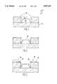
- FIG. 1 there is shown an initial stage 10 in the formation of a solder deposit in accordance with the invention.
- a conductor or pad 14 is simply supported on a planar substrate 12 but it is to be understood that layer 12 could be any layer of an integrated circuit or electronic package such as a so-called multi-layer module (MLM) capable of supporting and interconnecting a potentially large plurality of chips and that portions thereof could exhibit severe surface topography at other locations.
- MLM multi-layer module
- other conductors or pads could and normally would exist in close proximity to conductor or pad 14.
- a layer 16 of material which is not wettable by solder has been applied and patterned (as indicated by dashed line 18), possibly by lithographic or other high resolution techniques, to remove material around the area where the solder connection is to be made.
- This patterned layer 16 thus surrounds the interconnection region and serves to prevent solder migration during the subsequent soldering and/or desoldering process or processes. Since this layer preferably remains in place for this purpose, thickness of the layer is not critical for defining the volume of solder deposited in accordance with the invention.
- layer 16 be relatively thin since increased thickness beyond that which produces a layer with good integrity (and a sufficient volume of solder to dissolve layer 20 as will be discussed below) has no beneficial result and may reduce the effectiveness and/or reliability with which some of the further processes in accordance with the invention may be performed.
- patterning layer 16 allows for some degree of misregistration and preferably does not require patterning at the minimum feature size in accordance with the design rules of the device since the openings in layer 16 are preferably somewhat larger than the feature size represented by the width of conductor or pad 14.
- this tolerance need not be provided and may be precluded by some designs in which the invention may be employed and registration tolerances would be correspondingly more critical.
- a solder-wettable, conductive layer 20 is deposited over all surfaces of the device, including those to which solder is to be applied.
- Known electroless plating processes and vacuum sputtering have been found suitable for depositing such a layer of copper.
- good conductors other than copper would be extremely expensive and less conductive materials would require a greater thickness of layer 20 with consequent complication of the process.
- Gold also has low solubility and forms gold/tin intermetallic compounds and thus would have only a very marginal advantage over copper even if cost were neglected.
- Copper is generally preferred as such a solder-wettable material since copper has good adhesion, sufficient to the reliable practice of the invention, to most substrate and conductor materials and is low in cost.
- conductive layer 20 which must support later-deposited layer 30 during the electroplating process
- mechanically roughen e.g. by pumice scrubbing
- chemically modify e.g. with O 2 or CF 4 /O 2 plasma or chemical treatment with alkaline permanganate or sulfuric-chromic acid solutions and the like
- the particular treatment being chosen to avoid damage to connections or pads of particular metals, such as gold.
- Copper is also highly conductive and a relatively thin layer is sufficient for subsequent electroplating processes which will be described below.
- a sufficient thickness must be used to carry current for electroplating without causing a voltage gradient in the conductive layer 20 which would result in non-uniformity of deposition or heating which might damage the resist of the plating mask 30.
- copper it is somewhat critical that the layer 20 be kept as thin as possible due to the low solubility of copper in most solder materials, as discussed above.
- a patternable and removable dielectric layer 30 is formed over the solder-wettable layer 20 and patterned to form apertures preferably having a somewhat larger transverse dimension than the apertures in layer 16.
- the dielectric must be thick enough to contain the desired volume of solder material without “mushrooming" over the surface of layer 30 during plating. Dry film photoresists are particularly suitable for that reason. It is generally desirable to apply the dielectric layer 30 to both sides of the substrate to avoid deposition of solder on any exposed conductive surface other than those exposed by the patterning of layer 30.
- transverse dimension of these apertures between aperture edges 32 should be chosen in accordance with the thickness of the layer 30 since the volume of the aperture defines the amount of solder material which will be deposited in accordance with the invention.
- the larger transverse dimension provides a degree of registration tolerance in the patterning of layer 30.
- increased depth of the aperture due to thickness of layer 30 may compromise later processes. Accordingly, it is desirable that the transverse dimensions of the apertures be as large as possible to maintain sufficient separation between them and the layer 30 be correspondingly thin and only of sufficient thickness to define a desired volume of solder materials.
- desired solder volumes are generally in the range of 40 to 70 cubic mils (0.000,000,040 to 0.000,000,070 cubic inches).
- solder volumes can be determined empirically.
- layer 30 exposes solder wettable material at all locations at which solder connections are to be made and that all exposed locations of layer 20 are electrically connected.
- At least one additional aperture 34 (schematically depicted by dashed lines) must also be formed for an electrical connection to layer 20, in order to carry out the processes illustrated in FIGS. 4 and 8.
- metal solder material 40 is deposited on conductive layer 20 within apertures defined by apertures 32 and 16' by electroplating.
- the metal solder materials preferably tin and lead, may be deposited in a plurality of layers by sequential electroplating processes and/or by alloy electroplating. Other alloys such as tin-bismuth and lead indium and other combinations of electroplatable metals can be used.
- the electroplating process or processes are largely isotropic and thickness of the deposit is gradually built up from all conductor surfaces; thus allowing fine control of deposited solder volume within the volume coarsely defined by the apertures in both layers 16 and 30.
- the dielectric layer 30 is removed and the portions of layer 20 which are not covered by the deposited solder material are selectively etched away using selective etchants and processes well-understood in the art.
- the removal of these layers results in isolated lands of solder material but which are potentially slightly larger and possibly somewhat misregistered with the aperture 16'.
- Solder-wettable material of remaining portions of layer 20 also extend over a small region of the surface of layer 16 which, as indicated above, is intended to prevent solder migration during later soldering processes. Chemical treatment of the plated solder may optionally be done to remove contamination and residues from the stripping and etching processes.
- solder deposit prior to forming a solder connection.
- Application of heat to the device as shown in FIG. 5 sufficient to melt the solder material 40 causes the solder-wettable material of layer 20 to be dissolved in the solder material.
- the surface of layer 16 which is not solder-wettable is exposed. This causes the solder material to withdraw from the surface of layer 16 to locations within the edges 16' of the apertures and for the shape of the solder material to become raised at a point centered within the aperture and over the pad or connection 14.
- a domed shape of the solder deposit e.g. for self-registration with an aperture, application of flux and/or to make a contact centrally of an opposing pad to which a solder connection is to be made
- a domed shape may be desirable in many applications, however, some applications may require that the dome be flattened prior to forming a solder connection.
- the above-described process represents the most general methodology for practice of the invention, some minor variations are considered to be preferred for particular substrates and types of electronic packaging.
- the copper connections are preferably covered with a solder mask 30 of non-solder-wettable material to control the areas on which solder is deposited.
- the solder mask 30 is preferably of an organic polymer film that can be patterned by stenciling or by lithography processes after application.
- Aqueous processable solder resists are preferred since they exhibit a reduced tendency to leave residues in the apertures 16' which can interfere with plating and form inclusions in the solder.
- “tenting” e.g. bridging of the end of a plated through-hole which is useful, for example, where a plated through hole exists at a chip attachment location and where it is necessary to apply a reinforcing material as a low viscosity liquid to avoid fatigue of the solder joints and which would flow out of the plated through hole without closure of the hole by such tenting
- a dry film solder resist which naturally tents the plated through holes is preferred over liquid resist materials which do not.
- Non-solder wettable metal films such as chromium
- chromium can also be used since differential etch rates between chromium and copper and solder materials can be achieved by known processes and etchants.
- Aluminum is also non-solder wettable and thus also potentially useful.
- These variations of the invention are also appropriate for MLM's using a polyimide for the substrate of a layer to which solder is to be applied, molded circuit boards and metallized ceramic substrates. Additionally, with metallized ceramic substrates, layer 16 can be formed as a thick film dielectric and patterned by stenciling.
- a flexible dielectric preferably of similar material should be used for layer 16.
- solder mask materials similar to those used in printed circuit boards are satisfactory since flexure is not necessary during manufacture.
- interlayer connections are characteristically made by conductor filled through holes known as vias. Since the material surrounding the vias is not solder-wettable, a solder mask need not be separately provided and the ceramic layer itself, serves as a solder mask. If the via material is not solder-wettable, it can be made wettable by plating with a solder-wettable metal such as copper or gold.
- the invention may be applied to other structures and using other materials as the conductive layer 20 and dielectric layer 30 based on the above examples.
- the conductive layer 20 must be conductive, have good adhesion to conductors (in the event not all of the conductive layer material can be dissolved), selectively removable in comparison to the solder materials and wettable by those materials. In addition, some degree of solubility of the conductive material is desirable in order to cause the solder to pull back into aperture 16' when the solder is fused and reflowed.
- the dielectric layer 30 (which inhibits plating thereon) can be any material which can be patterned, easily removable and can withstand the chemicals used in the electroplating process.
- apertures 16' and 32 become of very small transverse dimension aspect ratio of the apertures (e.g. depth to width) may become larger. Either small transverse dimensions or increased aspect ratio may impede fluid flow and circulation (e.g. convection) within the apertures during the electroplating process and transport of metal particles or ions occurs substantially only through diffusion. Without such circulation, the electroplating fluids in the aperture rapidly become depleted of the material being plated onto exposed portions of conductive layer 20 and the solder deposits may require extended processing and/or be unreliably formed. That is, control of plating rate of the solder material is effectively lost.
- fluid flow and circulation e.g. convection
- Reduced plating rate also limits the electroplating current which can be used without evolution of hydrogen through electrolysis and further displace plating solutions from the surfaces on which deposition is desired. Voids observed in the plated layer(s), even when plating times are extended may be attributable to this mechanism, as well.
- Increase of the bulk concentration of the plated material in the solution to increase the concentration gradient and the diffusion rate but has also been found to have a detrimental effect on plating thickness and volume uniformity.
- a plating bath having a metal content of 20-40 grams/liter gives good plating uniformity (although such metal content may be varied considerably for different types of acid, additives and the like).
- the metal content is doubled or tripled (while other constituents of the bath composition remain generally unchanged) in order to significantly alter the concentration gradient, substantial reduction of plating uniformity will usually result.
- FIG. 7A An exemplary sparger is illustrated in FIG. 7A.
- the sparger size corresponds to a 10 inch by 15 inch panel outline and consists of four pipes 71 spaced three inches on center for a width of 12 inches, allowing for a 2.5 inch amplitude of panel motion for cathode agitation, shown by dashed and dotted lines 72, 73.
- Forty-four orifices 74 are provided, each having a diameter of one-eighth inch.
- FIG. 8 is a top view of this arrangement, including anode bars 75 spaced two inches behind the sparger which, in turn, is spaced at 3.5 inches from the panel surface.
- This arrangement provides a stagnation point of the jets near the surface of the panel with a solution flow rate of 5-10 gallons per minute. This positioning of the stagnation point maximizes turbulence of the fluid at the surface of the panel. A higher flow rate of 15 gallons per minute yielded unacceptable erosion of deposits. That is, since the stagnation point would be effectively "behind" the panel at the higher flow rate, erosion appears to be due to excessive fluid velocity and fluid force against the panel.
- Optimum cathode agitation using the arrangement of FIG. 8 was empirically determined to be 60-120 strokes per minute with a 2.5 inch stroke. This level of cathode agitation tends to optimally even out the localized variations in turbulence from the jets and provides a shearing action against the fluid which augments the effects of turbulence for providing circulation within the blind apertures. Further, using the arrangement of FIGS. 7A and 8, a current density of 15-25 amperes per square foot of plated area with a bath concentration of 14-40 grams per liter total metals (tin plus lead) and 250-350 grams per liter of free acid. This combination of conditions appears optimal from the standpoint of rapid material deposition while avoiding generation of hydrogen gas by electrolysis; providing good deposit uniformity and absence of voids, resulting in high production yield closely approaching 100%.
- FIG. 7B and 7C A variation of the manifold of FIG. 7A is shown in FIG. 7B and 7C.
- the orifices 76 are smaller (e.g. 1/16 inch) and more numerous as well as being arranged in rows at 45° to the boundaries of the sparger at a closer spacing. This has been found to provide more uniform turbulence over the surface of the panel. The greater uniformity of turbulence does not require adjustment of cathode agitation stroke and closer spacing of jets effectively provides a higher frequency of local variation of turbulence at any point on the panel during the cathode agitation stroke. (Note that 4 ⁇ 0.75 inches equals the three inch spacing in the embodiment of FIG. 7B.)
- the alternative sparger includes a further array of relatively larger (e.g. 1/4 inch) openings 77 interspersed among the jet orifices 76 discussed above. These orifices are formed by tubes, as best shown in FIG. 7C, which communicate between the exterior of the sparger and a return plenum 79 located behind the source plenum 78 which supplies fluid to the jets 76.
- This array of return openings 77 substantially avoids the development of directionality in the average flow across the panel. Development of directionality of flow is cumulative across the panel over the distance from any jet to any return inlet and the effects are generally manifested as substantial changes in deposition thickness toward the panel edges if the return inlets are provided outside the panel area.
- the arrangement of a return inlet between each pair of jets in both coordinate directions is highly effective in avoiding cumulative development of flow directionality across the panel.
- the total area of the jet orifices in the embodiment of FIGS. 7B and 7C is comparable to that of the embodiment shown in FIG. 7A so that the flow rates and the geometry of the individual fluid jets is comparable. Therefore, similar plating bath concentrations and plating currents can be used with either sparger embodiment.
- the much greater area of the return openings 77 compared to the jet orifices 76 assure that little effect on the individual jets will be produced thereby.
- a second problem encountered when the invention is applied to the formation of extremely small deposits at the present limit of lithographic technology is due to the reduced volume of solder materials available for dissolution of copper. That is, a reduction in transverse dimensions of a solder deposit will cause a much larger proportionate decrease in the volume of the solder deposit even if the thickness of layers 16 and 30 remains the same. While the surface area plated with copper will decrease somewhat, the volume of the solder will decrease far more and thus, for a given thickness of copper, the ratio of copper volume to solder volume will increase significantly as transverse dimension of the solder deposit is decreased.
- the thickness of the solder deposit defined by layers 16 and 30 will often be reduced as well, both to reduce the volume of solder which could form bridge connections to other conductors or pads as spacing is reduced and to hold the aspect ratio of blind apertures to a suitable value as transverse dimensions of the deposit are decreased.
- the solubility of copper in solder materials is very low and molten solder can be easily saturated with copper and copper-tin intermetallic compounds may be formed which precipitate from the solder material as the solder is cooled and may significantly affect the alloy composition and melting point of the solder.
- connection or pad 14 can also be a significant additional source of copper.
- an additional step is provided in the methodology discussed above in regard to FIGS. 1-6.
- the device is treated in an immersion bath for a length of time sufficient for replacing substantially all the exposed copper in layer 20 with tin or other material which is a constituent of the intended solder alloy, as indicated by arrow 92, to form a deposit of solder constituent material 20'. That is, any remaining trace amount of copper for which the solder constituent material is not substituted should be less than the amount of copper that can be readily dissolved in the solder material.
- the timing of this process may be empirically determined. No replacement of copper occurs at unexposed locations of layer 20 and the resulting deposits of tin or other solder constituent material remain electrically connected to each other and the source of electroplating current with a highly conductive copper grid.
- the remainder of the process steps described above in regard to FIGS. 4-6 can be performed to complete the solder material deposit.
- the electroplating process proceeds precisely as before since the replacement metal remains electrically connected by a low resistance copper grid which can carry sufficient current for the purpose.
- Layer 30 can then be removed in precisely the same manner and the same selective etchants can be used to selectively remove the remaining portions of copper layer 20 without attacking the solder deposits.
- the solder material can be reflowed and will draw back to the aperture 16' as described above since layer 16 is not solder-wettable but without the need to dissolve more than trace amounts of copper in the solder.
- conductive layer 20 of tin does not provide satisfactory results, largely because of inherently lower adhesion of tin to layer 16 which tends to flake off and contaminate the surface.
- the adhesion is certainly insufficient to support layer 30 during electroplating.
- This lower adhesion cannot be avoided since layer 16 must be of a non-solder wettable material.
- a greater thickness of tin or other material would be required to carry the electroplating current. This additional thickness, itself, presents a further complication since etchants effective to remove portions of layer 20 between the solder deposits after electroplating would also attack the solder deposits.
- Suitable immersion baths for this purpose are known for use in manufacture of printed circuit boards but have been used only for the replacement of a thin surface layer of the copper.
- immersion baths containing tin, lead or a combination thereof are known and possible for the practice of the invention. Pure tin should be used for copper replacement if tin/bismuth solder materials are to be deposited. Otherwise, a tin/lead combination which closely matches the intended relative concentrations in the solder materials to be deposited will allow closest regulation of the melting point of the total solder deposit when the replacement material becomes mixed with the remainder of the solder material. Between pure tin and pure lead replacement materials, pure tin is preferred since variation of the tin content of solder has less effect on melting point of solder than a comparable variation in lead content.
- this variation of the invention is considered to be advantageous for several other reason, as well.
- two passes are required through an infra-red reflow oven, each followed by a deionized water cleaning step to obtain complete dewetting of the surface of the solder from the solder mask layer 16 and (especially where apertures 16' are large, relative to the dimensions of pad or connection 14, the surface of card dielectric layer or substrate 12) to obtain complete pull-back of the solder onto the circuit connections or pads 14.
- a mildly activated, water cleanable flux is also required for each of these reflows.
- the flux used for reflow can be chosen from fluxes (e.g. non-activated, "no-clean" fluxes) suitable for making solder connections. Therefore, the connection of chips, modules and/or boards can be done concurrently with the reflow step, further reducing process steps and complexity. Also, as alluded to above, the rounded or domed upper surface of the solder deposit formed by the drawing back of solder during reflow may not be desirable in some applications, in which case, a further process step for flattening of the solder deposits is avoided, as well.
- fluxes e.g. non-activated, "no-clean" fluxes
- Another advantage of this variation of the invention is that in cases where the aperture 16' is significantly larger than pad or connection 14, as alluded to above, it is desirable for maximizing the amount of solder in the joint and minimization of parasitic capacitance of the joint that the solder pull back from both the sides 16' of the aperture in layer 16 and the surface 12' of layer or substrate 12 as shown in FIG. 10.
- solder constituent material 20' Since the deposit of solder constituent material 20' has been substituted for the exposed portion of copper layer 20, when solder deposit 40 is reflowed, possibly while making a solder connection to pad or connection 120 of device 110 (with or without C4 preform 100), the solder constituent material is immediately incorporated into the deposited solder material, any trace amounts of copper are immediately dissolved in the solder material and the solder will immediately withdraw from unwettable surfaces 12', 16' of layers 12, 16 and assume a stable meniscus-like shape 40' only between wettable surfaces of pads or connections 14 and 120.
- the methodology and apparatus of the invention can provide solder deposits of high uniformity both in volume and shape which are particularly suitable for closely spaced connections and feature sizes which can be formed at the present state of lithographic technology and in which the content of low-solubility materials in the solder connection may be controlled to the point of substantial elimination.
Landscapes
- Engineering & Computer Science (AREA)
- Microelectronics & Electronic Packaging (AREA)
- Chemical & Material Sciences (AREA)
- Manufacturing & Machinery (AREA)
- Power Engineering (AREA)
- Computer Hardware Design (AREA)
- Materials Engineering (AREA)
- Organic Chemistry (AREA)
- Metallurgy (AREA)
- Electrochemistry (AREA)
- Chemical Kinetics & Catalysis (AREA)
- Physics & Mathematics (AREA)
- Condensed Matter Physics & Semiconductors (AREA)
- General Physics & Mathematics (AREA)
- Ceramic Engineering (AREA)
- Manufacturing Of Printed Wiring (AREA)
- Electric Connection Of Electric Components To Printed Circuits (AREA)
- Electroplating Methods And Accessories (AREA)
Priority Applications (7)
| Application Number | Priority Date | Filing Date | Title |
|---|---|---|---|
| US08/387,686 US5597469A (en) | 1995-02-13 | 1995-02-13 | Process for selective application of solder to circuit packages |
| TW084108830A TW404156B (en) | 1995-02-13 | 1995-08-24 | Process for selective application of solder to circuit packages |
| KR1019950061276A KR100225217B1 (ko) | 1995-02-13 | 1995-12-28 | 회로 패키지에 땜납을 선택적으로 용착시키는 공정 및 그 공정을 위한 전기도금 장치 |
| EP96100324A EP0726698A3 (en) | 1995-02-13 | 1996-01-11 | Method for the selective application of solder to circuit packages |
| US08/585,819 US5656139A (en) | 1995-02-13 | 1996-01-16 | Electroplating apparatus |
| JP02393096A JP3655961B2 (ja) | 1995-02-13 | 1996-02-09 | 回路パッケージに半田を選択的に付着する方法 |
| US08/633,322 US5672260A (en) | 1995-02-13 | 1996-04-17 | Process for selective application of solder to circuit packages |
Applications Claiming Priority (1)
| Application Number | Priority Date | Filing Date | Title |
|---|---|---|---|
| US08/387,686 US5597469A (en) | 1995-02-13 | 1995-02-13 | Process for selective application of solder to circuit packages |
Related Child Applications (2)
| Application Number | Title | Priority Date | Filing Date |
|---|---|---|---|
| US08/585,819 Division US5656139A (en) | 1995-02-13 | 1996-01-16 | Electroplating apparatus |
| US08/633,322 Continuation US5672260A (en) | 1995-02-13 | 1996-04-17 | Process for selective application of solder to circuit packages |
Publications (1)
| Publication Number | Publication Date |
|---|---|
| US5597469A true US5597469A (en) | 1997-01-28 |
Family
ID=23530959
Family Applications (3)
| Application Number | Title | Priority Date | Filing Date |
|---|---|---|---|
| US08/387,686 Expired - Fee Related US5597469A (en) | 1995-02-13 | 1995-02-13 | Process for selective application of solder to circuit packages |
| US08/585,819 Expired - Lifetime US5656139A (en) | 1995-02-13 | 1996-01-16 | Electroplating apparatus |
| US08/633,322 Expired - Lifetime US5672260A (en) | 1995-02-13 | 1996-04-17 | Process for selective application of solder to circuit packages |
Family Applications After (2)
| Application Number | Title | Priority Date | Filing Date |
|---|---|---|---|
| US08/585,819 Expired - Lifetime US5656139A (en) | 1995-02-13 | 1996-01-16 | Electroplating apparatus |
| US08/633,322 Expired - Lifetime US5672260A (en) | 1995-02-13 | 1996-04-17 | Process for selective application of solder to circuit packages |
Country Status (5)
| Country | Link |
|---|---|
| US (3) | US5597469A (ko) |
| EP (1) | EP0726698A3 (ko) |
| JP (1) | JP3655961B2 (ko) |
| KR (1) | KR100225217B1 (ko) |
| TW (1) | TW404156B (ko) |
Cited By (25)
| Publication number | Priority date | Publication date | Assignee | Title |
|---|---|---|---|---|
| WO1998012738A1 (en) * | 1996-09-20 | 1998-03-26 | Lsi Logic Corporation | Fluxless solder ball attachment process |
| US5808853A (en) * | 1996-10-31 | 1998-09-15 | International Business Machines Corporation | Capacitor with multi-level interconnection technology |
| US5872051A (en) * | 1995-08-02 | 1999-02-16 | International Business Machines Corporation | Process for transferring material to semiconductor chip conductive pads using a transfer substrate |
| US5898992A (en) * | 1996-04-30 | 1999-05-04 | Pressac Limited | Method of mounting circuit components on a flexible substrate |
| US5985123A (en) * | 1997-07-09 | 1999-11-16 | Koon; Kam Kwan | Continuous vertical plating system and method of plating |
| US6117299A (en) * | 1997-05-09 | 2000-09-12 | Mcnc | Methods of electroplating solder bumps of uniform height on integrated circuit substrates |
| US6336262B1 (en) | 1996-10-31 | 2002-01-08 | International Business Machines Corporation | Process of forming a capacitor with multi-level interconnection technology |
| US6378759B1 (en) * | 2000-07-18 | 2002-04-30 | Chartered Semiconductor Manufacturing Ltd. | Method of application of conductive cap-layer in flip-chip, COB, and micro metal bonding |
| US6427901B2 (en) * | 1999-06-30 | 2002-08-06 | Lucent Technologies Inc. | System and method for forming stable solder bonds |
| US6492600B1 (en) | 1999-06-28 | 2002-12-10 | International Business Machines Corporation | Laminate having plated microvia interconnects and method for forming the same |
| US6510976B2 (en) * | 2001-05-18 | 2003-01-28 | Advanpack Solutions Pte. Ltd. | Method for forming a flip chip semiconductor package |
| US6527163B1 (en) * | 2000-01-21 | 2003-03-04 | Tessera, Inc. | Methods of making bondable contacts and a tool for making such contacts |
| US6674647B2 (en) | 2002-01-07 | 2004-01-06 | International Business Machines Corporation | Low or no-force bump flattening structure and method |
| US20040087053A1 (en) * | 2002-10-31 | 2004-05-06 | Motorola Inc. | Low cost fabrication and assembly of lid for semiconductor devices |
| US20040155097A1 (en) * | 2003-02-04 | 2004-08-12 | Matsushita Electric Industrial Co., Ltd. | Soldering method and method for manufacturing component mounting board |
| US6861345B2 (en) * | 1999-08-27 | 2005-03-01 | Micron Technology, Inc. | Method of disposing conductive bumps onto a semiconductor device |
| US20050140009A1 (en) * | 2002-06-17 | 2005-06-30 | Horst Groeninger | Method and apparatus for the production of an electronic component with external contact areas |
| US20060099727A1 (en) * | 2004-10-21 | 2006-05-11 | Endicott Interconnect Technologies, Inc. | Method of making a circuitized substrate having a plurality of solder connection sites thereon |
| US20060113680A1 (en) * | 1997-09-18 | 2006-06-01 | Tessera, Inc. | Microelectronic packages with solder interconnections |
| US20070090170A1 (en) * | 2005-10-20 | 2007-04-26 | Endicott Interconnect Technologies, Inc. | Method of making a circuitized substrate having a plurality of solder connection sites thereon |
| US7427423B2 (en) * | 1998-03-26 | 2008-09-23 | Tessera, Inc. | Components with conductive solder mask layers |
| US20090127704A1 (en) * | 2007-11-20 | 2009-05-21 | Fujitsu Limited | Method and System for Providing a Reliable Semiconductor Assembly |
| US20090218124A1 (en) * | 2008-02-28 | 2009-09-03 | Motorola, Inc. | Method of filling vias with fusible metal |
| US20170125329A1 (en) * | 2015-10-30 | 2017-05-04 | International Business Machines Corporation | Method for forming solder bumps using sacrificial layer |
| US11114406B2 (en) * | 2019-01-31 | 2021-09-07 | Sandisk Technologies Llc | Warpage-compensated bonded structure including a support chip and a three-dimensional memory chip |
Families Citing this family (37)
| Publication number | Priority date | Publication date | Assignee | Title |
|---|---|---|---|---|
| DE19820345C2 (de) * | 1997-04-17 | 2000-05-25 | Univ Dresden Tech | Verfahren zum selektiven galvanischen Aufbringen von Lotdepots auf Leiterplatten |
| DE19716044C2 (de) * | 1997-04-17 | 1999-04-08 | Univ Dresden Tech | Verfahren zum selektiven galvanischen Aufbringen von Lotdepots auf Leiterplatten |
| US6962997B1 (en) * | 1997-05-22 | 2005-11-08 | Celgene Corporation | Process and intermediates for resolving piperidyl acetamide steroisomers |
| US6156408A (en) * | 1997-08-29 | 2000-12-05 | Motorola, Inc. | Device for reworkable direct chip attachment |
| US6074895A (en) * | 1997-09-23 | 2000-06-13 | International Business Machines Corporation | Method of forming a flip chip assembly |
| US6818110B1 (en) | 1997-09-30 | 2004-11-16 | Symyx Technologies, Inc. | Combinatorial electrochemical deposition and testing system |
| US6187164B1 (en) | 1997-09-30 | 2001-02-13 | Symyx Technologies, Inc. | Method for creating and testing a combinatorial array employing individually addressable electrodes |
| JPH11145176A (ja) * | 1997-11-11 | 1999-05-28 | Fujitsu Ltd | ハンダバンプの形成方法及び予備ハンダの形成方法 |
| JP4066522B2 (ja) * | 1998-07-22 | 2008-03-26 | イビデン株式会社 | プリント配線板 |
| DE19860587A1 (de) * | 1998-12-29 | 2000-07-06 | Bosch Gmbh Robert | Verfahren zur Verbindung zweier Oberflächen und Vorrichtung |
| JP3056192B1 (ja) * | 1999-01-18 | 2000-06-26 | 富山日本電気株式会社 | 電極パッド上にバンプを形成したソルダーレジスト層付実装基板の製造方法 |
| US6341071B1 (en) | 1999-03-19 | 2002-01-22 | International Business Machines Corporation | Stress relieved ball grid array package |
| US6047637A (en) * | 1999-06-17 | 2000-04-11 | Fujitsu Limited | Method of paste printing using stencil and masking layer |
| US6570251B1 (en) * | 1999-09-02 | 2003-05-27 | Micron Technology, Inc. | Under bump metalization pad and solder bump connections |
| JP3403677B2 (ja) * | 1999-09-06 | 2003-05-06 | マイクロ・テック株式会社 | 半田ボール形成方法 |
| US6547937B1 (en) * | 2000-01-03 | 2003-04-15 | Semitool, Inc. | Microelectronic workpiece processing tool including a processing reactor having a paddle assembly for agitation of a processing fluid proximate to the workpiece |
| US6469394B1 (en) * | 2000-01-31 | 2002-10-22 | Fujitsu Limited | Conductive interconnect structures and methods for forming conductive interconnect structures |
| EP1432293A4 (en) | 2001-09-28 | 2005-12-07 | Ibiden Co Ltd | PCB AND MANUFACTURING PROCESS FOR THE PCB |
| WO2003107413A2 (de) * | 2002-06-17 | 2003-12-24 | Infineon Technologies Ag | Verfahren und vorrichtung für die herstellung eines elektronischen bauteils mit aussenkontaktflächen |
| US7393439B2 (en) | 2003-06-06 | 2008-07-01 | Semitool, Inc. | Integrated microfeature workpiece processing tools with registration systems for paddle reactors |
| US7390382B2 (en) | 2003-07-01 | 2008-06-24 | Semitool, Inc. | Reactors having multiple electrodes and/or enclosed reciprocating paddles, and associated methods |
| US7313462B2 (en) | 2003-06-06 | 2007-12-25 | Semitool, Inc. | Integrated tool with automated calibration system and interchangeable wet processing components for processing microfeature workpieces |
| US20050005436A1 (en) * | 2003-07-09 | 2005-01-13 | Jung-Chien Chang | Method for preparing thin integrated circuits with multiple circuit layers |
| US20050085062A1 (en) * | 2003-10-15 | 2005-04-21 | Semitool, Inc. | Processes and tools for forming lead-free alloy solder precursors |
| TWI231028B (en) * | 2004-05-21 | 2005-04-11 | Via Tech Inc | A substrate used for fine-pitch semiconductor package and a method of the same |
| EP1865550A4 (en) * | 2005-03-29 | 2012-07-11 | Panasonic Corp | FLIPCHIP APPLICATION METHOD AND METHOD FOR CONNECTING SUBSTRATES |
| JP4319647B2 (ja) * | 2005-06-30 | 2009-08-26 | 株式会社タムラ古河マシナリー | リフロー炉 |
| JP4738971B2 (ja) * | 2005-10-14 | 2011-08-03 | Okiセミコンダクタ株式会社 | 半導体装置及びその製造方法 |
| JP4764718B2 (ja) * | 2005-12-28 | 2011-09-07 | 新光電気工業株式会社 | スルーホールの充填方法 |
| US20080116077A1 (en) * | 2006-11-21 | 2008-05-22 | M/A-Com, Inc. | System and method for solder bump plating |
| DE102007026633B4 (de) * | 2007-06-06 | 2009-04-02 | Atotech Deutschland Gmbh | Vorrichtung und Verfahren zum elektrolytischen Behandeln von plattenförmiger Ware |
| US8313984B2 (en) * | 2008-03-19 | 2012-11-20 | Ati Technologies Ulc | Die substrate with reinforcement structure |
| JP5501940B2 (ja) * | 2010-11-15 | 2014-05-28 | 欣興電子股▲フン▼有限公司 | 回路板の製造方法 |
| US9142520B2 (en) * | 2011-08-30 | 2015-09-22 | Ati Technologies Ulc | Methods of fabricating semiconductor chip solder structures |
| JP5410580B1 (ja) * | 2012-08-09 | 2014-02-05 | 日本特殊陶業株式会社 | 配線基板 |
| KR101506910B1 (ko) * | 2012-09-27 | 2015-03-30 | 티디케이가부시기가이샤 | 이방성 도금 방법 및 박막 코일 |
| CN111893533B (zh) * | 2020-07-26 | 2022-12-06 | 中国航发贵州红林航空动力控制科技有限公司 | 一种花瓣形转子局部电镀铅铟合金的方法 |
Citations (27)
| Publication number | Priority date | Publication date | Assignee | Title |
|---|---|---|---|---|
| US3554878A (en) * | 1968-07-02 | 1971-01-12 | North American Rockwell | Plating tin-lead alloy on printed circuits and electrolyte therefor |
| US3850765A (en) * | 1973-05-21 | 1974-11-26 | Oxy Metal Finishing Corp | Bright solder plating |
| US3875029A (en) * | 1974-02-19 | 1975-04-01 | R O Hull & Company Inc | Plating bath for electrodeposition of bright tin and tin-lead alloy |
| US3905878A (en) * | 1970-11-16 | 1975-09-16 | Hyogo Prefectural Government | Electrolyte for and method of bright electroplating of tin-lead alloy |
| US4000047A (en) * | 1972-11-17 | 1976-12-28 | Lea-Ronal, Inc. | Electrodeposition of tin, lead and tin-lead alloys |
| US4153523A (en) * | 1978-05-04 | 1979-05-08 | Bell Telephone Laboratories, Incorporated | Continuous electrochemical processing apparatus |
| US4186062A (en) * | 1978-07-13 | 1980-01-29 | Micro-Plate, Inc. | Continuous tab plater and method |
| US4217182A (en) * | 1978-06-07 | 1980-08-12 | Litton Systems, Inc. | Semi-additive process of manufacturing a printed circuit |
| US4220506A (en) * | 1978-12-11 | 1980-09-02 | Bell Telephone Laboratories, Incorporated | Process for plating solder |
| US4263106A (en) * | 1979-12-31 | 1981-04-21 | Bell Telephone Laboratories, Incorporated | Solder plating process |
| US4289846A (en) * | 1979-12-28 | 1981-09-15 | General Electric Company | Process for forming low-reactance interconnections on semiconductors |
| US4293637A (en) * | 1977-05-31 | 1981-10-06 | Matsushita Electric Industrial Co., Ltd. | Method of making metal electrode of semiconductor device |
| US4304640A (en) * | 1978-12-20 | 1981-12-08 | Nevin Electric Limited | Method of plating solder onto printed circuit boards |
| US4358349A (en) * | 1979-05-24 | 1982-11-09 | Matsushita Electric Works, Ltd. | Method of forming electrical wiring path on insulative substrate |
| US4487654A (en) * | 1983-10-27 | 1984-12-11 | Ael Microtel Limited | Method of manufacturing printed wiring boards |
| US4526859A (en) * | 1983-12-12 | 1985-07-02 | International Business Machines Corporation | Metallization of a ceramic substrate |
| US4560445A (en) * | 1984-12-24 | 1985-12-24 | Polyonics Corporation | Continuous process for fabricating metallic patterns on a thin film substrate |
| US4569743A (en) * | 1983-09-23 | 1986-02-11 | International Business Machines Corporation | Method and apparatus for the selective, self-aligned deposition of metal layers |
| US4586990A (en) * | 1982-03-15 | 1986-05-06 | Gsp Metals & Chemicals Corporation | Chelating metals |
| US4589962A (en) * | 1985-06-03 | 1986-05-20 | National Semiconductor Corporation | Solder plating process and semiconductor product |
| US4640739A (en) * | 1984-08-16 | 1987-02-03 | Robert Bosch Gmbh | Process of producing galvanic layers of solder of precise contour on inorganic substrates |
| US4790912A (en) * | 1985-06-06 | 1988-12-13 | Techno-Instruments Investments Ltd. | Selective plating process for the electrolytic coating of circuit boards without an electroless metal coating |
| US4863808A (en) * | 1985-09-13 | 1989-09-05 | Gould Inc. | Copper-chromium-polyimide composite |
| US4925525A (en) * | 1988-04-11 | 1990-05-15 | Minolta Camera Kabushiki Kaisha | Process for producing a printed circuit board |
| US5028513A (en) * | 1988-04-13 | 1991-07-02 | Hitachi, Ltd. | Process for producing printed circuit board |
| US5194137A (en) * | 1991-08-05 | 1993-03-16 | Motorola Inc. | Solder plate reflow method for forming solder-bumped terminals |
| US5316788A (en) * | 1991-07-26 | 1994-05-31 | International Business Machines Corporation | Applying solder to high density substrates |
Family Cites Families (11)
| Publication number | Priority date | Publication date | Assignee | Title |
|---|---|---|---|---|
| US3275542A (en) * | 1962-10-26 | 1966-09-27 | Gen Instrument Corp | Apparatus for electroplating leads of small electronic components |
| US3397126A (en) * | 1965-10-14 | 1968-08-13 | Sel Rex Corp | Plating of small parts |
| US3477051A (en) * | 1967-12-26 | 1969-11-04 | Ibm | Die casting of core windings |
| US3503856A (en) * | 1968-01-30 | 1970-03-31 | Rotary Plates Ltd | Process for controlling electrodeposition |
| DE2630688A1 (de) * | 1976-07-08 | 1978-01-12 | Bosch Gmbh Robert | Verfahren zur herstellung galvanischer kupferschichten fuer leiterzuege auf leiterplatten |
| US4459183A (en) * | 1981-10-07 | 1984-07-10 | Chemcut Corporation | Electroplating apparatus and method |
| US4443304A (en) * | 1982-10-01 | 1984-04-17 | Micro-Plate, Inc. | Plating system and method |
| US4686014A (en) * | 1984-11-23 | 1987-08-11 | Pellegrino Peter P | Turbulent cell electroplating method and apparatus |
| JPH0671133B2 (ja) * | 1988-01-30 | 1994-09-07 | イビデン株式会社 | プリント配線板における半田層の形成方法 |
| US4861425A (en) * | 1988-08-22 | 1989-08-29 | International Business Machines Corporation | Lift-off process for terminal metals |
| DE4310930A1 (de) * | 1993-04-02 | 1994-10-06 | Siemens Ag | Leiterplattenanordnung und Verfahren zur Herstellung einer bestückten Leiterplatte |
-
1995
- 1995-02-13 US US08/387,686 patent/US5597469A/en not_active Expired - Fee Related
- 1995-08-24 TW TW084108830A patent/TW404156B/zh not_active IP Right Cessation
- 1995-12-28 KR KR1019950061276A patent/KR100225217B1/ko not_active IP Right Cessation
-
1996
- 1996-01-11 EP EP96100324A patent/EP0726698A3/en not_active Withdrawn
- 1996-01-16 US US08/585,819 patent/US5656139A/en not_active Expired - Lifetime
- 1996-02-09 JP JP02393096A patent/JP3655961B2/ja not_active Expired - Lifetime
- 1996-04-17 US US08/633,322 patent/US5672260A/en not_active Expired - Lifetime
Patent Citations (27)
| Publication number | Priority date | Publication date | Assignee | Title |
|---|---|---|---|---|
| US3554878A (en) * | 1968-07-02 | 1971-01-12 | North American Rockwell | Plating tin-lead alloy on printed circuits and electrolyte therefor |
| US3905878A (en) * | 1970-11-16 | 1975-09-16 | Hyogo Prefectural Government | Electrolyte for and method of bright electroplating of tin-lead alloy |
| US4000047A (en) * | 1972-11-17 | 1976-12-28 | Lea-Ronal, Inc. | Electrodeposition of tin, lead and tin-lead alloys |
| US3850765A (en) * | 1973-05-21 | 1974-11-26 | Oxy Metal Finishing Corp | Bright solder plating |
| US3875029A (en) * | 1974-02-19 | 1975-04-01 | R O Hull & Company Inc | Plating bath for electrodeposition of bright tin and tin-lead alloy |
| US4293637A (en) * | 1977-05-31 | 1981-10-06 | Matsushita Electric Industrial Co., Ltd. | Method of making metal electrode of semiconductor device |
| US4153523A (en) * | 1978-05-04 | 1979-05-08 | Bell Telephone Laboratories, Incorporated | Continuous electrochemical processing apparatus |
| US4217182A (en) * | 1978-06-07 | 1980-08-12 | Litton Systems, Inc. | Semi-additive process of manufacturing a printed circuit |
| US4186062A (en) * | 1978-07-13 | 1980-01-29 | Micro-Plate, Inc. | Continuous tab plater and method |
| US4220506A (en) * | 1978-12-11 | 1980-09-02 | Bell Telephone Laboratories, Incorporated | Process for plating solder |
| US4304640A (en) * | 1978-12-20 | 1981-12-08 | Nevin Electric Limited | Method of plating solder onto printed circuit boards |
| US4358349A (en) * | 1979-05-24 | 1982-11-09 | Matsushita Electric Works, Ltd. | Method of forming electrical wiring path on insulative substrate |
| US4289846A (en) * | 1979-12-28 | 1981-09-15 | General Electric Company | Process for forming low-reactance interconnections on semiconductors |
| US4263106A (en) * | 1979-12-31 | 1981-04-21 | Bell Telephone Laboratories, Incorporated | Solder plating process |
| US4586990A (en) * | 1982-03-15 | 1986-05-06 | Gsp Metals & Chemicals Corporation | Chelating metals |
| US4569743A (en) * | 1983-09-23 | 1986-02-11 | International Business Machines Corporation | Method and apparatus for the selective, self-aligned deposition of metal layers |
| US4487654A (en) * | 1983-10-27 | 1984-12-11 | Ael Microtel Limited | Method of manufacturing printed wiring boards |
| US4526859A (en) * | 1983-12-12 | 1985-07-02 | International Business Machines Corporation | Metallization of a ceramic substrate |
| US4640739A (en) * | 1984-08-16 | 1987-02-03 | Robert Bosch Gmbh | Process of producing galvanic layers of solder of precise contour on inorganic substrates |
| US4560445A (en) * | 1984-12-24 | 1985-12-24 | Polyonics Corporation | Continuous process for fabricating metallic patterns on a thin film substrate |
| US4589962A (en) * | 1985-06-03 | 1986-05-20 | National Semiconductor Corporation | Solder plating process and semiconductor product |
| US4790912A (en) * | 1985-06-06 | 1988-12-13 | Techno-Instruments Investments Ltd. | Selective plating process for the electrolytic coating of circuit boards without an electroless metal coating |
| US4863808A (en) * | 1985-09-13 | 1989-09-05 | Gould Inc. | Copper-chromium-polyimide composite |
| US4925525A (en) * | 1988-04-11 | 1990-05-15 | Minolta Camera Kabushiki Kaisha | Process for producing a printed circuit board |
| US5028513A (en) * | 1988-04-13 | 1991-07-02 | Hitachi, Ltd. | Process for producing printed circuit board |
| US5316788A (en) * | 1991-07-26 | 1994-05-31 | International Business Machines Corporation | Applying solder to high density substrates |
| US5194137A (en) * | 1991-08-05 | 1993-03-16 | Motorola Inc. | Solder plate reflow method for forming solder-bumped terminals |
Non-Patent Citations (4)
| Title |
|---|
| "Method of Connecting Layers of Circuitry Separated by a Dielectric"; IBM Technical Disclosure Bulletin; vol. 22, No. 10, Mar. 1980; O. R. Abolafia; pp. 4471-4473. |
| "Passivation Process for Semiconductor Device With Fusible Link Redundancy"; IBM Technical Disclosure Bulletin; vol. 23, No. 10, Mar. 1981; D. E. Davis, W. T. Motsiff and N. R. Poulin; pp. 4451-4452. |
| Method of Connecting Layers of Circuitry Separated by a Dielectric ; IBM Technical Disclosure Bulletin; vol. 22, No. 10, Mar. 1980; O. R. Abolafia; pp. 4471 4473. * |
| Passivation Process for Semiconductor Device With Fusible Link Redundancy ; IBM Technical Disclosure Bulletin; vol. 23, No. 10, Mar. 1981; D. E. Davis, W. T. Motsiff and N. R. Poulin; pp. 4451 4452. * |
Cited By (37)
| Publication number | Priority date | Publication date | Assignee | Title |
|---|---|---|---|---|
| US5872051A (en) * | 1995-08-02 | 1999-02-16 | International Business Machines Corporation | Process for transferring material to semiconductor chip conductive pads using a transfer substrate |
| US5898992A (en) * | 1996-04-30 | 1999-05-04 | Pressac Limited | Method of mounting circuit components on a flexible substrate |
| WO1998012738A1 (en) * | 1996-09-20 | 1998-03-26 | Lsi Logic Corporation | Fluxless solder ball attachment process |
| US5899737A (en) * | 1996-09-20 | 1999-05-04 | Lsi Logic Corporation | Fluxless solder ball attachment process |
| US5808853A (en) * | 1996-10-31 | 1998-09-15 | International Business Machines Corporation | Capacitor with multi-level interconnection technology |
| US6336262B1 (en) | 1996-10-31 | 2002-01-08 | International Business Machines Corporation | Process of forming a capacitor with multi-level interconnection technology |
| US6117299A (en) * | 1997-05-09 | 2000-09-12 | Mcnc | Methods of electroplating solder bumps of uniform height on integrated circuit substrates |
| US5985123A (en) * | 1997-07-09 | 1999-11-16 | Koon; Kam Kwan | Continuous vertical plating system and method of plating |
| US7078819B2 (en) * | 1997-09-18 | 2006-07-18 | Tessera, Inc. | Microelectronic packages with elongated solder interconnections |
| US20060113680A1 (en) * | 1997-09-18 | 2006-06-01 | Tessera, Inc. | Microelectronic packages with solder interconnections |
| US7427423B2 (en) * | 1998-03-26 | 2008-09-23 | Tessera, Inc. | Components with conductive solder mask layers |
| US6492600B1 (en) | 1999-06-28 | 2002-12-10 | International Business Machines Corporation | Laminate having plated microvia interconnects and method for forming the same |
| US7328506B2 (en) | 1999-06-28 | 2008-02-12 | International Business Machines Corporation | Method for forming a plated microvia interconnect |
| US20080017410A1 (en) * | 1999-06-28 | 2008-01-24 | Jimarez Miguel A | Method for forming a plated microvia interconnect |
| US6427901B2 (en) * | 1999-06-30 | 2002-08-06 | Lucent Technologies Inc. | System and method for forming stable solder bonds |
| US20050142835A1 (en) * | 1999-08-27 | 2005-06-30 | Ball Michael B. | Method of disposing conductive bumps onto a semiconductor device and semiconductor devices so formed |
| US6861345B2 (en) * | 1999-08-27 | 2005-03-01 | Micron Technology, Inc. | Method of disposing conductive bumps onto a semiconductor device |
| US6527163B1 (en) * | 2000-01-21 | 2003-03-04 | Tessera, Inc. | Methods of making bondable contacts and a tool for making such contacts |
| US6378759B1 (en) * | 2000-07-18 | 2002-04-30 | Chartered Semiconductor Manufacturing Ltd. | Method of application of conductive cap-layer in flip-chip, COB, and micro metal bonding |
| US6510976B2 (en) * | 2001-05-18 | 2003-01-28 | Advanpack Solutions Pte. Ltd. | Method for forming a flip chip semiconductor package |
| US6674647B2 (en) | 2002-01-07 | 2004-01-06 | International Business Machines Corporation | Low or no-force bump flattening structure and method |
| US20050140009A1 (en) * | 2002-06-17 | 2005-06-30 | Horst Groeninger | Method and apparatus for the production of an electronic component with external contact areas |
| US20040087053A1 (en) * | 2002-10-31 | 2004-05-06 | Motorola Inc. | Low cost fabrication and assembly of lid for semiconductor devices |
| US6949398B2 (en) | 2002-10-31 | 2005-09-27 | Freescale Semiconductor, Inc. | Low cost fabrication and assembly of lid for semiconductor devices |
| CN100400217C (zh) * | 2003-02-04 | 2008-07-09 | 松下电器产业株式会社 | 焊接方法和制备元件安装板的方法 |
| US20040155097A1 (en) * | 2003-02-04 | 2004-08-12 | Matsushita Electric Industrial Co., Ltd. | Soldering method and method for manufacturing component mounting board |
| US7087441B2 (en) | 2004-10-21 | 2006-08-08 | Endicott Interconnect Technologies, Inc. | Method of making a circuitized substrate having a plurality of solder connection sites thereon |
| US20060099727A1 (en) * | 2004-10-21 | 2006-05-11 | Endicott Interconnect Technologies, Inc. | Method of making a circuitized substrate having a plurality of solder connection sites thereon |
| US20070090170A1 (en) * | 2005-10-20 | 2007-04-26 | Endicott Interconnect Technologies, Inc. | Method of making a circuitized substrate having a plurality of solder connection sites thereon |
| US20090127704A1 (en) * | 2007-11-20 | 2009-05-21 | Fujitsu Limited | Method and System for Providing a Reliable Semiconductor Assembly |
| US8487428B2 (en) * | 2007-11-20 | 2013-07-16 | Fujitsu Limited | Method and system for providing a reliable semiconductor assembly |
| US20090218124A1 (en) * | 2008-02-28 | 2009-09-03 | Motorola, Inc. | Method of filling vias with fusible metal |
| US20170125329A1 (en) * | 2015-10-30 | 2017-05-04 | International Business Machines Corporation | Method for forming solder bumps using sacrificial layer |
| US9953908B2 (en) * | 2015-10-30 | 2018-04-24 | International Business Machines Corporation | Method for forming solder bumps using sacrificial layer |
| US20180218970A1 (en) * | 2015-10-30 | 2018-08-02 | International Business Machines Corporation | Method for forming solder bumps using sacrificial layer |
| US10535592B2 (en) | 2015-10-30 | 2020-01-14 | International Business Machines Corporation | Method for forming solder bumps using sacrificial layer |
| US11114406B2 (en) * | 2019-01-31 | 2021-09-07 | Sandisk Technologies Llc | Warpage-compensated bonded structure including a support chip and a three-dimensional memory chip |
Also Published As
| Publication number | Publication date |
|---|---|
| EP0726698A3 (en) | 1996-11-20 |
| JPH08242071A (ja) | 1996-09-17 |
| KR100225217B1 (ko) | 1999-10-15 |
| US5656139A (en) | 1997-08-12 |
| KR960032575A (ko) | 1996-09-17 |
| TW404156B (en) | 2000-09-01 |
| EP0726698A2 (en) | 1996-08-14 |
| JP3655961B2 (ja) | 2005-06-02 |
| US5672260A (en) | 1997-09-30 |
Similar Documents
| Publication | Publication Date | Title |
|---|---|---|
| US5597469A (en) | Process for selective application of solder to circuit packages | |
| KR100188625B1 (ko) | 인쇄 회로 기판상에 미세 피치 땜납 피착 방법 및 그 제품 | |
| US6469394B1 (en) | Conductive interconnect structures and methods for forming conductive interconnect structures | |
| JP3469686B2 (ja) | プリント回路基板上にはんだを付着させる方法およびプリント回路基板 | |
| US5672542A (en) | Method of making solder balls by contained paste deposition | |
| US7830667B2 (en) | Flexible wiring substrate and method for producing the same | |
| US6436803B2 (en) | Manufacturing computer systems with fine line circuitized substrates | |
| US7087441B2 (en) | Method of making a circuitized substrate having a plurality of solder connection sites thereon | |
| US8871631B2 (en) | Method to form solder deposits on substrates | |
| KR20130113409A (ko) | 기판 상에 솔더 합금 성막을 형성하는 방법 | |
| US20070090170A1 (en) | Method of making a circuitized substrate having a plurality of solder connection sites thereon | |
| KR100557549B1 (ko) | 플립칩 범프 패드 형성 방법 및 그 구조 | |
| KR100275400B1 (ko) | 인쇄 회로 기판 및 반도체 패키지 | |
| JP3434829B2 (ja) | 端子面のハンダ付け方法及びハンダ合金の製造方法 | |
| US20060011482A1 (en) | Electrocodeposition of lead free tin alloys | |
| JP4015667B2 (ja) | メッキ基板のエッチング装置 | |
| US7910156B2 (en) | Method of making circuitized substrate with selected conductors having solder thereon | |
| KR100589071B1 (ko) | 프린트 배선 기재 및 전해 주석계 합금 도금 방법 | |
| US20220059439A1 (en) | Solder printing | |
| EP2244285A1 (en) | Method to form solder deposits on substrates | |
| US7071026B2 (en) | Production method for making film carrier tape for mounting electronic devices thereon | |
| JP3246623B2 (ja) | はんだ付け装置及びはんだ付け方法 | |
| KR940009173B1 (ko) | 프린트 기판의 제조방법 | |
| JP3565556B2 (ja) | 錫−ビスマス合金メッキ装置及びメッキ方法 | |
| JPH0766559A (ja) | 多層回路基板の配線層間接続構造及び該接続構造の形成方法 |
Legal Events
| Date | Code | Title | Description |
|---|---|---|---|
| AS | Assignment |
Owner name: INTERNATIONAL BUSINESS MACHINES CORPORATION, NEW Y Free format text: ASSIGNMENT OF ASSIGNORS INTEREST;ASSIGNORS:CAREY, CHARLES FRANCIS;FALLON, KENNETH MICHAEL;MARKOVICH, VOYA RISTA;AND OTHERS;REEL/FRAME:007367/0376;SIGNING DATES FROM 19950203 TO 19950207 |
|
| FEPP | Fee payment procedure |
Free format text: PAYOR NUMBER ASSIGNED (ORIGINAL EVENT CODE: ASPN); ENTITY STATUS OF PATENT OWNER: LARGE ENTITY |
|
| FEPP | Fee payment procedure |
Free format text: PAYOR NUMBER ASSIGNED (ORIGINAL EVENT CODE: ASPN); ENTITY STATUS OF PATENT OWNER: LARGE ENTITY |
|
| FEPP | Fee payment procedure |
Free format text: PAYER NUMBER DE-ASSIGNED (ORIGINAL EVENT CODE: RMPN); ENTITY STATUS OF PATENT OWNER: LARGE ENTITY |
|
| FPAY | Fee payment |
Year of fee payment: 4 |
|
| REMI | Maintenance fee reminder mailed | ||
| LAPS | Lapse for failure to pay maintenance fees | ||
| STCH | Information on status: patent discontinuation |
Free format text: PATENT EXPIRED DUE TO NONPAYMENT OF MAINTENANCE FEES UNDER 37 CFR 1.362 |
|
| FP | Lapsed due to failure to pay maintenance fee |
Effective date: 20050128 |