US10347525B2 - Method for producing bonded SOI wafer - Google Patents
Method for producing bonded SOI wafer Download PDFInfo
- Publication number
- US10347525B2 US10347525B2 US15/767,174 US201615767174A US10347525B2 US 10347525 B2 US10347525 B2 US 10347525B2 US 201615767174 A US201615767174 A US 201615767174A US 10347525 B2 US10347525 B2 US 10347525B2
- Authority
- US
- United States
- Prior art keywords
- wafer
- layer
- soi
- oxide film
- film thickness
- Prior art date
- Legal status (The legal status is an assumption and is not a legal conclusion. Google has not performed a legal analysis and makes no representation as to the accuracy of the status listed.)
- Active
Links
Images


Classifications
-
- H—ELECTRICITY
- H01—ELECTRIC ELEMENTS
- H01L—SEMICONDUCTOR DEVICES NOT COVERED BY CLASS H10
- H01L21/00—Processes or apparatus adapted for the manufacture or treatment of semiconductor or solid state devices or of parts thereof
- H01L21/02—Manufacture or treatment of semiconductor devices or of parts thereof
- H01L21/04—Manufacture or treatment of semiconductor devices or of parts thereof the devices having at least one potential-jump barrier or surface barrier, e.g. PN junction, depletion layer or carrier concentration layer
- H01L21/18—Manufacture or treatment of semiconductor devices or of parts thereof the devices having at least one potential-jump barrier or surface barrier, e.g. PN junction, depletion layer or carrier concentration layer the devices having semiconductor bodies comprising elements of Group IV of the Periodic System or AIIIBV compounds with or without impurities, e.g. doping materials
- H01L21/185—Joining of semiconductor bodies for junction formation
-
- H—ELECTRICITY
- H01—ELECTRIC ELEMENTS
- H01L—SEMICONDUCTOR DEVICES NOT COVERED BY CLASS H10
- H01L21/00—Processes or apparatus adapted for the manufacture or treatment of semiconductor or solid state devices or of parts thereof
- H01L21/70—Manufacture or treatment of devices consisting of a plurality of solid state components formed in or on a common substrate or of parts thereof; Manufacture of integrated circuit devices or of parts thereof
- H01L21/71—Manufacture of specific parts of devices defined in group H01L21/70
- H01L21/76—Making of isolation regions between components
- H01L21/762—Dielectric regions, e.g. EPIC dielectric isolation, LOCOS; Trench refilling techniques, SOI technology, use of channel stoppers
- H01L21/7624—Dielectric regions, e.g. EPIC dielectric isolation, LOCOS; Trench refilling techniques, SOI technology, use of channel stoppers using semiconductor on insulator [SOI] technology
- H01L21/76251—Dielectric regions, e.g. EPIC dielectric isolation, LOCOS; Trench refilling techniques, SOI technology, use of channel stoppers using semiconductor on insulator [SOI] technology using bonding techniques
- H01L21/76254—Dielectric regions, e.g. EPIC dielectric isolation, LOCOS; Trench refilling techniques, SOI technology, use of channel stoppers using semiconductor on insulator [SOI] technology using bonding techniques with separation/delamination along an ion implanted layer, e.g. Smart-cut, Unibond
-
- H—ELECTRICITY
- H01—ELECTRIC ELEMENTS
- H01L—SEMICONDUCTOR DEVICES NOT COVERED BY CLASS H10
- H01L21/00—Processes or apparatus adapted for the manufacture or treatment of semiconductor or solid state devices or of parts thereof
- H01L21/02—Manufacture or treatment of semiconductor devices or of parts thereof
- H01L21/02104—Forming layers
- H01L21/02107—Forming insulating materials on a substrate
- H01L21/02225—Forming insulating materials on a substrate characterised by the process for the formation of the insulating layer
- H01L21/0226—Forming insulating materials on a substrate characterised by the process for the formation of the insulating layer formation by a deposition process
- H01L21/02293—Forming insulating materials on a substrate characterised by the process for the formation of the insulating layer formation by a deposition process formation of epitaxial layers by a deposition process
-
- H—ELECTRICITY
- H01—ELECTRIC ELEMENTS
- H01L—SEMICONDUCTOR DEVICES NOT COVERED BY CLASS H10
- H01L21/00—Processes or apparatus adapted for the manufacture or treatment of semiconductor or solid state devices or of parts thereof
- H01L21/02—Manufacture or treatment of semiconductor devices or of parts thereof
- H01L21/04—Manufacture or treatment of semiconductor devices or of parts thereof the devices having at least one potential-jump barrier or surface barrier, e.g. PN junction, depletion layer or carrier concentration layer
- H01L21/18—Manufacture or treatment of semiconductor devices or of parts thereof the devices having at least one potential-jump barrier or surface barrier, e.g. PN junction, depletion layer or carrier concentration layer the devices having semiconductor bodies comprising elements of Group IV of the Periodic System or AIIIBV compounds with or without impurities, e.g. doping materials
- H01L21/26—Bombardment with radiation
- H01L21/263—Bombardment with radiation with high-energy radiation
- H01L21/265—Bombardment with radiation with high-energy radiation producing ion implantation
-
- H—ELECTRICITY
- H01—ELECTRIC ELEMENTS
- H01L—SEMICONDUCTOR DEVICES NOT COVERED BY CLASS H10
- H01L21/00—Processes or apparatus adapted for the manufacture or treatment of semiconductor or solid state devices or of parts thereof
- H01L21/02—Manufacture or treatment of semiconductor devices or of parts thereof
- H01L21/04—Manufacture or treatment of semiconductor devices or of parts thereof the devices having at least one potential-jump barrier or surface barrier, e.g. PN junction, depletion layer or carrier concentration layer
- H01L21/18—Manufacture or treatment of semiconductor devices or of parts thereof the devices having at least one potential-jump barrier or surface barrier, e.g. PN junction, depletion layer or carrier concentration layer the devices having semiconductor bodies comprising elements of Group IV of the Periodic System or AIIIBV compounds with or without impurities, e.g. doping materials
- H01L21/30—Treatment of semiconductor bodies using processes or apparatus not provided for in groups H01L21/20 - H01L21/26
- H01L21/324—Thermal treatment for modifying the properties of semiconductor bodies, e.g. annealing, sintering
-
- H—ELECTRICITY
- H01—ELECTRIC ELEMENTS
- H01L—SEMICONDUCTOR DEVICES NOT COVERED BY CLASS H10
- H01L21/00—Processes or apparatus adapted for the manufacture or treatment of semiconductor or solid state devices or of parts thereof
- H01L21/70—Manufacture or treatment of devices consisting of a plurality of solid state components formed in or on a common substrate or of parts thereof; Manufacture of integrated circuit devices or of parts thereof
- H01L21/71—Manufacture of specific parts of devices defined in group H01L21/70
- H01L21/76—Making of isolation regions between components
- H01L21/762—Dielectric regions, e.g. EPIC dielectric isolation, LOCOS; Trench refilling techniques, SOI technology, use of channel stoppers
- H01L21/7624—Dielectric regions, e.g. EPIC dielectric isolation, LOCOS; Trench refilling techniques, SOI technology, use of channel stoppers using semiconductor on insulator [SOI] technology
- H01L21/76243—Dielectric regions, e.g. EPIC dielectric isolation, LOCOS; Trench refilling techniques, SOI technology, use of channel stoppers using semiconductor on insulator [SOI] technology using silicon implanted buried insulating layers, e.g. oxide layers, i.e. SIMOX techniques
-
- H—ELECTRICITY
- H01—ELECTRIC ELEMENTS
- H01L—SEMICONDUCTOR DEVICES NOT COVERED BY CLASS H10
- H01L21/00—Processes or apparatus adapted for the manufacture or treatment of semiconductor or solid state devices or of parts thereof
- H01L21/70—Manufacture or treatment of devices consisting of a plurality of solid state components formed in or on a common substrate or of parts thereof; Manufacture of integrated circuit devices or of parts thereof
- H01L21/77—Manufacture or treatment of devices consisting of a plurality of solid state components or integrated circuits formed in, or on, a common substrate
- H01L21/78—Manufacture or treatment of devices consisting of a plurality of solid state components or integrated circuits formed in, or on, a common substrate with subsequent division of the substrate into plural individual devices
- H01L21/7806—Manufacture or treatment of devices consisting of a plurality of solid state components or integrated circuits formed in, or on, a common substrate with subsequent division of the substrate into plural individual devices involving the separation of the active layers from a substrate
-
- H—ELECTRICITY
- H01—ELECTRIC ELEMENTS
- H01L—SEMICONDUCTOR DEVICES NOT COVERED BY CLASS H10
- H01L27/00—Devices consisting of a plurality of semiconductor or other solid-state components formed in or on a common substrate
- H01L27/02—Devices consisting of a plurality of semiconductor or other solid-state components formed in or on a common substrate including semiconductor components specially adapted for rectifying, oscillating, amplifying or switching and having at least one potential-jump barrier or surface barrier; including integrated passive circuit elements with at least one potential-jump barrier or surface barrier
- H01L27/12—Devices consisting of a plurality of semiconductor or other solid-state components formed in or on a common substrate including semiconductor components specially adapted for rectifying, oscillating, amplifying or switching and having at least one potential-jump barrier or surface barrier; including integrated passive circuit elements with at least one potential-jump barrier or surface barrier the substrate being other than a semiconductor body, e.g. an insulating body
Definitions
- the present invention relates to a method for producing a bonded SOI wafer and, in particular, relates to a method for producing a SOI wafer by using an ion implantation delamination method.
- SOT Silicon on Insulator
- a method for producing a thin-film SOI wafer that can enhance the performance of a leading-edge integrated circuit a method for producing a SOI wafer by delaminating an ion implanted wafer after bonding (an ion implantation delamination method: the technology also called SmartCut® process) has attracted attention.
- an ion implantation delamination method the technology also called SmartCut® process
- the cleavage plane (the delaminating plane) is the surface of a SOI layer, and a SOI wafer whose SOI film thickness is small and has a high degree of uniformity is obtained with relative ease.
- a damaged layer caused by ion implantation is present on the surface of the SOI wafer subjected to delamination, and the surface roughness is greater than that of a mirror surface of a normal silicon wafer.
- Patent Document 1 WO 2003/009386
- Patent Document 2 WO 2011/027545
- a bonded SOI wafer having a BOX layer (a buried oxide film layer) and a SOI layer on a base wafer is fabricated by the ion implantation delamination method and the delaminated surface is flattened by heat treatment in an argon gas-containing atmosphere (hereinafter also referred to simply as Ar annealing), etching of the SOI/BOX interface and the BOX/base wafer interface progresses and the foundation BOX layer disappears at the outermost peripheral part of the SOI layer, which sometimes causes the outermost peripheral part of the SOT layer to be left in the form of an overhang shortly after Ar annealing.
- Ar annealing argon gas-containing atmosphere
- the present invention has been made in view of the problem described above and an object thereof is to prevent, in the production of a bonded SOI wafer, the generation of particles from the outermost peripheral part, which is left in the form of an overhang by flattening heat treatment in an argon gas-containing atmosphere, of a SOI layer.
- the present invention provides a method for producing a bonded SOI wafer, by forming an ion implanted layer by implanting at least one type of gas ion of a hydrogen ion and a rare gas ion from a surface of a bond wafer formed of a silicon single crystal and, after bonding together the ion implanted surface of the bond wafer and a surface of a base wafer formed of a silicon single crystal with a silicon oxide film placed therebetween, delaminating the bond wafer at the ion implanted layer to fabricate a bonded SOI wafer having a BOX layer and a SOT layer on a base wafer and, after performing flattening heat treatment on the bonded SOI wafer in an argon gas-containing atmosphere, sacrificial oxidation treatment that adjusts the film thickness of the SOI layer is performed, wherein the film thickness of the BOX layer in the bonded SOI wafer fabricated by the delamination is set so as to be 500 nm
- the argon gas-containing atmosphere is 100% Ar gas.
- the present invention it is preferable that, by forming a silicon oxide film which is 500 nm or more on the base wafer and, after bonding together the base wafer on which the silicon oxide film is formed and the ion implanted surface of the bond wafer, delaminating the bond wafer at the ion implanted layer, the bonded SOI wafer with the BOX layer whose film thickness is 500 nm or more is fabricated.
- an epitaxial layer may also be formed on the surface of the SOI layer subjected to the sacrificial oxidation treatment.
- the SOI layer is usually limited to a thin-film SOI layer which is thinner than 1 ⁇ m. For this reason, in order to produce a bonded SOI wafer having a SOI layer whose film thickness is a few ⁇ m or more and film thickness uniformity is high, it is necessary to additionally form an epitaxial layer on the surface of the thin-film SOI layer fabricated by the ion implantation delamination method. Also in such a case, with the present invention, it is possible to prevent the generation of particles from the outermost peripheral part of the SOI layer and also suppress the generation of defects at the time of formation of the epitaxial layer.
- the present invention by adjusting a sacrificial oxide film thickness in sacrificial oxidation treatment after Ar annealing so that the overhang-shaped outermost peripheral part of a SOI layer completely changes into a sacrificial oxide film, it is possible to prevent the generation of particles from the outermost peripheral part, which is left in the form of an overhang after Ar annealing, of the SOT layer.
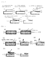
- FIG. 1 is a process flow diagram showing an example of a method for producing a bonded SOI wafer of the present invention
- FIG. 2 is an explanatory diagram of a mechanism by which the outermost peripheral part of a SOI layer is left in the form of an overhang after Ar annealing and a particle generation mechanism;
- FIG. 3 is an explanatory diagram depicting an example of the method for producing a bonded SOI wafer of the present invention
- FIG. 4 shows (A) a SEM image of a bonded SOI wafer in a state in which a thin film (SOI+BOX) has widely exfoliated, (B) a SEM image of the state in which erosion at the SOI/BOX interface has progressed, and (C) a SEM image of the state in which erosion at the BOX/base wafer interface has progressed; and
- FIG. 5 is an explanatory diagram depicting the relationship between the film thickness (t) of a SOI layer on which a sacrificial oxidation treatment is to be performed and the film thickness (d) of a sacrificial oxide film which is formed by sacrificial oxidation treatment in the present invention.
- bonding heat treatment is sometimes performed in an oxidizing atmosphere.
- a surface oxide film 13 by the bonding heat treatment is formed on the surface of the SOI layer 11 after delamination ( FIG. 2( a ) ).
- the surface oxide film 13 formed by the bonding heat treatment is removed by using hydrofluoric acid, for example ( FIG. 2( b ) ).
- sacrificial oxidation treatment formation of a sacrificial oxide film 17 ( FIG. 2( d ) )+oxide film removal ( FIG. 2( e ) )
- sacrificial oxidation treatment formation of a sacrificial oxide film 17 ( FIG. 2( d ) )+oxide film removal ( FIG. 2( e ) )
- the film thickness of this formed sacrificial oxide film 17 is an insufficient thickness, the outer peripheral part of the SOI layer is thinly left in the form of an overhang after oxide film removal, which causes the thin outer peripheral part of the SOI layer to exfoliate in subsequent processes such as cleaning and become a particle.
- the inventor of the present invention has found that, if the thickness of a BOX layer becomes 500 nm or more, a thin film (SOI+BOX) exfoliates noticeably, a wider overhang shape is formed, and the generation of particles also becomes noticeable. Then, the inventor of the present invention has found that, for a bonded SOI wafer with a BOX layer whose thickness is 500 nm or more, by adjusting a sacrificial oxide film thickness in sacrificial oxidation after Ar annealing so that the overhang-shaped outer peripheral part of a SOI layer completely changes into an oxide film, it is possible to prevent the generation of particles from the outermost peripheral part, which is left in the form of an overhang, of the SOI layer.
- FIG. 1 illustrates a process flow diagram showing an example of a method for producing a bonded SOI wafer of the present invention.
- FIG. 3 illustrates an explanatory diagram depicting an example of the method for producing a bonded SOI wafer of the present invention.
- an ion implanted layer is formed at a predetermined depth of the bond wafer ( FIG. 1(A) ).
- a silicon oxide film which becomes a BOX layer (with a film thickness of 500 nm or more) later, is formed on the bond wafer and/or a base wafer. If such a thick oxide film is formed on the bond wafer, it is necessary to make an acceleration voltage for ion implantation extremely high, which requires an ion implantation apparatus that can perform high-voltage ion implantation. For this reason, in the present invention, it is preferable to form a silicon oxide film which is 500 nm or more on the base wafer ( FIG. 1(B) ). It goes without saying that a silicon oxide film may be formed on both the bond wafer and the base wafer in such a way that the total thickness of the silicon oxide films becomes 500 nm or more.
- the base wafer on which the silicon oxide film is formed and the ion implanted surface of the bond wafer are bonded together ( FIG. 1(C) ).
- This bonding is performed as follows: by making the bond wafer and the base wafer come into contact with each other in a clean atmosphere at room temperature, for example, the wafers are bonded together without use of an adhesive or the like.
- a bonded SOI wafer having, on the base wafer, a buried oxide film layer (a BOX layer) whose film thickness is 500 nm or more and a SOI layer is fabricated ( FIG. 1(D) ).
- a BOX layer buried oxide film layer
- SOI layer a SOI layer is fabricated ( FIG. 1(D) ).
- this delamination heat treatment for example, by performing heat treatment in an inert gas atmosphere such as Ar at usually 400° C. or higher and 700° C. or lower for 30 minutes or more, the bond wafer can be delaminated at the ion implanted layer.
- the bond wafer can also be delaminated by applying an external force without performing heat treatment (or after performing heat treatment at a temperature at which delamination does not occur). It is to be noted that an upper limit of the film thickness of the buried oxide film layer can be set at 5 ⁇ m, for example.
- bonding heat treatment in an oxidizing atmosphere may be performed and then processing to remove the formed surface oxide film may be performed.
- oxide film formation and oxide film removal it is possible to remove implantation damage caused at the time of ion implantation and left on the delaminated surface.
- a thermal oxide film 3 is formed on a base wafer 2 ( FIG. 3(A) )
- the base wafer 2 is bonded to a bond wafer having no oxide film, and a bonded SOI wafer is fabricated by the ion implantation delamination method ( FIG. 3(B) )
- an interface A between a SOI layer 1 and a BOX layer 3 is a bonding interface
- an interface B between the BOX layer 3 and the base wafer 2 is a thermal oxide film interface.
- compressive strain is kept in the thermal oxide film 3 (the BOX layer) formed on the base wafer 2 .
- the thickness of the BOX layer 3 is 500 nm or more as in the present invention, the thin film (SOI+BOX) exfoliates noticeably and a wider overhang shape is formed.
- Such a phenomenon occurs in an argon-containing atmosphere (for example, a mixed gas atmosphere of argon and hydrogen or a 100% Ar gas atmosphere) and, in particular, occurs noticeably by heat treatment which is performed in a 100% Ar gas atmosphere for a long time (30 minutes or more) at a high temperature of 1150° C. or higher.
- an argon-containing atmosphere for example, a mixed gas atmosphere of argon and hydrogen or a 100% Ar gas atmosphere
- heat treatment which is performed in a 100% Ar gas atmosphere for a long time (30 minutes or more) at a high temperature of 1150° C. or higher.
- FIG. 4(A) A SEM image of a bonded SOI wafer in a state in which, when Ar annealing is performed on a bonded wafer having a BOX layer 3 : a film thickness of 1000 nm and a SOI layer 1 : a film thickness of 750 nm, a thin film (SOI+BOX) has widely exfoliated is shown in FIG. 4(A) .
- a SEM image of the state in which erosion has progressed at a SOI/BOX interface A is shown in FIG. 4(B)
- a SEM image of the state in which erosion has progressed at a BOX/base wafer interface B is shown in FIG. 4(C) .
- sacrificial oxidation treatment formation of a sacrificial oxide film 4 +oxide film removal
- sacrificial oxidation treatment formation of a sacrificial oxide film 4 +oxide film removal
- a sacrificial oxide film thickness is adjusted by adjusting the sacrificial oxidation conditions so that the overhang-shaped outer peripheral part of the SOI layer 1 completely changes into the sacrificial oxide film 4 .
- the sacrificial oxidation conditions such as an oxidation temperature and an oxidation time
- the sacrificial oxide film thickness (d) in such a way that 0.9d>t>0.45d is satisfied, it is possible to suppress the generation of particles caused by an overhang-shaped portion of a SOI layer.
- the conditions for sacrificial oxidation heat treatment are not limited to particular conditions as long as the conditions that a sacrificial oxide film whose film thickness satisfies 0.9d>t>0.45d can be formed; for example, by performing sacrificial oxidation heat treatment at a temperature of about 900 to 950° C., it is possible to enhance the bonding interface bond strength while sufficiently removing damage on a delaminated surface (a SOI layer surface) without the generation of oxidation-induced stacking faults (OSFs).
- OSFs oxidation-induced stacking faults
- the sacrificial oxide film formed by the sacrificial oxidation treatment is removed ( FIG. 3(G) ).
- the outer peripheral part, which is left in the form of an overhang after Ar annealing, of the SOI layer is completely removed.
- an oxide film removal method there is a method by which, for example, 15% HF cleaning and, if necessary, RCA cleaning are performed.
- the BOX layer is etched to an area slightly closer to the inside than the SOI layer, which results in a structure in which the end face of the BOX layer is recessed from the end face of the SOI layer.
- Example the effect of greatly reducing the generation of particles in a cleaning process after sacrificial oxidation treatment as compared to Comparative Example could be obtained.
Applications Claiming Priority (3)
| Application Number | Priority Date | Filing Date | Title |
|---|---|---|---|
| JP2015211730A JP6473970B2 (ja) | 2015-10-28 | 2015-10-28 | 貼り合わせsoiウェーハの製造方法 |
| JP2015-211730 | 2015-10-28 | ||
| PCT/JP2016/003916 WO2017072994A1 (ja) | 2015-10-28 | 2016-08-29 | 貼り合わせsoiウェーハの製造方法 |
Publications (2)
| Publication Number | Publication Date |
|---|---|
| US20190074213A1 US20190074213A1 (en) | 2019-03-07 |
| US10347525B2 true US10347525B2 (en) | 2019-07-09 |
Family
ID=58630023
Family Applications (1)
| Application Number | Title | Priority Date | Filing Date |
|---|---|---|---|
| US15/767,174 Active US10347525B2 (en) | 2015-10-28 | 2016-08-29 | Method for producing bonded SOI wafer |
Country Status (8)
| Country | Link |
|---|---|
| US (1) | US10347525B2 (ko) |
| EP (1) | EP3370249B1 (ko) |
| JP (1) | JP6473970B2 (ko) |
| KR (1) | KR102317552B1 (ko) |
| CN (1) | CN108140553B (ko) |
| SG (2) | SG10201903932WA (ko) |
| TW (1) | TWI709999B (ko) |
| WO (1) | WO2017072994A1 (ko) |
Families Citing this family (1)
| Publication number | Priority date | Publication date | Assignee | Title |
|---|---|---|---|---|
| CN111146146B (zh) * | 2019-12-30 | 2022-09-06 | 长春理工大学 | 一种基底可多次利用的高效散热半导体衬底的制备方法 |
Citations (10)
| Publication number | Priority date | Publication date | Assignee | Title |
|---|---|---|---|---|
| JPH0964321A (ja) | 1995-08-24 | 1997-03-07 | Komatsu Electron Metals Co Ltd | Soi基板の製造方法 |
| WO2003009386A1 (fr) | 2001-07-17 | 2003-01-30 | Shin-Etsu Handotai Co.,Ltd. | Procede de production de plaquettes de liaison |
| JP2006270039A (ja) | 2005-02-28 | 2006-10-05 | Shin Etsu Handotai Co Ltd | 貼り合わせウエーハの製造方法及び貼り合わせウエーハ |
| JP2007317988A (ja) | 2006-05-29 | 2007-12-06 | Shin Etsu Handotai Co Ltd | 貼り合わせウエーハの製造方法 |
| US20080315349A1 (en) | 2005-02-28 | 2008-12-25 | Shin-Etsu Handotai Co., Ltd. | Method for Manufacturing Bonded Wafer and Bonded Wafer |
| JP2009027124A (ja) | 2007-06-21 | 2009-02-05 | Shin Etsu Handotai Co Ltd | Soiウェーハの製造方法 |
| WO2011027545A1 (ja) | 2009-09-04 | 2011-03-10 | 信越半導体株式会社 | Soiウェーハの製造方法 |
| JP2012129347A (ja) | 2010-12-15 | 2012-07-05 | Shin Etsu Handotai Co Ltd | 貼り合わせsoiウエーハの製造方法 |
| US20180144975A1 (en) * | 2015-06-15 | 2018-05-24 | Shin-Etsu Handotai Co., Ltd. | Method for producing soi wafer |
| US20190035639A1 (en) * | 2016-02-19 | 2019-01-31 | Shin-Etsu Handotai Co., Ltd. | Heat treatment method for semiconductor wafer |
Family Cites Families (7)
| Publication number | Priority date | Publication date | Assignee | Title |
|---|---|---|---|---|
| JPH11204452A (ja) * | 1998-01-13 | 1999-07-30 | Mitsubishi Electric Corp | 半導体基板の処理方法および半導体基板 |
| JP4228419B2 (ja) * | 1998-07-29 | 2009-02-25 | 信越半導体株式会社 | Soiウエーハの製造方法およびsoiウエーハ |
| JP5135935B2 (ja) * | 2007-07-27 | 2013-02-06 | 信越半導体株式会社 | 貼り合わせウエーハの製造方法 |
| JP5499428B2 (ja) * | 2007-09-07 | 2014-05-21 | 株式会社Sumco | 貼り合わせウェーハの製造方法 |
| EP2075830A3 (en) * | 2007-10-11 | 2011-01-19 | Sumco Corporation | Method for producing bonded wafer |
| JP5521561B2 (ja) * | 2010-01-12 | 2014-06-18 | 信越半導体株式会社 | 貼り合わせウェーハの製造方法 |
| JP6056516B2 (ja) * | 2013-02-01 | 2017-01-11 | 信越半導体株式会社 | Soiウェーハの製造方法及びsoiウェーハ |
-
2015
- 2015-10-28 JP JP2015211730A patent/JP6473970B2/ja active Active
-
2016
- 2016-08-29 EP EP16859235.0A patent/EP3370249B1/en active Active
- 2016-08-29 KR KR1020187011656A patent/KR102317552B1/ko active IP Right Grant
- 2016-08-29 WO PCT/JP2016/003916 patent/WO2017072994A1/ja active Application Filing
- 2016-08-29 SG SG10201903932WA patent/SG10201903932WA/en unknown
- 2016-08-29 US US15/767,174 patent/US10347525B2/en active Active
- 2016-08-29 CN CN201680059158.3A patent/CN108140553B/zh active Active
- 2016-08-29 SG SG11201802984RA patent/SG11201802984RA/en unknown
- 2016-09-01 TW TW105128176A patent/TWI709999B/zh active
Patent Citations (15)
| Publication number | Priority date | Publication date | Assignee | Title |
|---|---|---|---|---|
| JPH0964321A (ja) | 1995-08-24 | 1997-03-07 | Komatsu Electron Metals Co Ltd | Soi基板の製造方法 |
| US5863829A (en) | 1995-08-24 | 1999-01-26 | Komatsu Electronic Metals Co., Ltd. | Process for fabricating SOI substrate |
| WO2003009386A1 (fr) | 2001-07-17 | 2003-01-30 | Shin-Etsu Handotai Co.,Ltd. | Procede de production de plaquettes de liaison |
| US20030181001A1 (en) * | 2001-07-17 | 2003-09-25 | Hiroji Aga | Method for producing bonding wafer |
| US20080315349A1 (en) | 2005-02-28 | 2008-12-25 | Shin-Etsu Handotai Co., Ltd. | Method for Manufacturing Bonded Wafer and Bonded Wafer |
| JP2006270039A (ja) | 2005-02-28 | 2006-10-05 | Shin Etsu Handotai Co Ltd | 貼り合わせウエーハの製造方法及び貼り合わせウエーハ |
| JP2007317988A (ja) | 2006-05-29 | 2007-12-06 | Shin Etsu Handotai Co Ltd | 貼り合わせウエーハの製造方法 |
| US20090170285A1 (en) | 2006-05-29 | 2009-07-02 | Shin-Etsu Handotai Co., Ltd. | Method for manufacturing bonded wafer |
| JP2009027124A (ja) | 2007-06-21 | 2009-02-05 | Shin Etsu Handotai Co Ltd | Soiウェーハの製造方法 |
| US20100129993A1 (en) | 2007-06-21 | 2010-05-27 | Shin-Etsu Handotai Co., Ltd. | Method for manufacturing soi wafer |
| WO2011027545A1 (ja) | 2009-09-04 | 2011-03-10 | 信越半導体株式会社 | Soiウェーハの製造方法 |
| US20120135584A1 (en) | 2009-09-04 | 2012-05-31 | Shin-Etsu Handotai Co., Ltd. | Method for manufacturing soi wafer |
| JP2012129347A (ja) | 2010-12-15 | 2012-07-05 | Shin Etsu Handotai Co Ltd | 貼り合わせsoiウエーハの製造方法 |
| US20180144975A1 (en) * | 2015-06-15 | 2018-05-24 | Shin-Etsu Handotai Co., Ltd. | Method for producing soi wafer |
| US20190035639A1 (en) * | 2016-02-19 | 2019-01-31 | Shin-Etsu Handotai Co., Ltd. | Heat treatment method for semiconductor wafer |
Non-Patent Citations (3)
| Title |
|---|
| May 1, 2018 International Preliminary Report on Patentability issued in International Patent Application No. PCT/JP2016/003916. |
| May 15, 2018 Office Action issued in Japanese Patent Application No. 2015-211730. |
| Nov. 1, 2016 International Search Report issued in International Patent Application No. PCT/JP2016/003916. |
Also Published As
| Publication number | Publication date |
|---|---|
| KR102317552B1 (ko) | 2021-10-27 |
| US20190074213A1 (en) | 2019-03-07 |
| WO2017072994A1 (ja) | 2017-05-04 |
| JP2017084963A (ja) | 2017-05-18 |
| SG11201802984RA (en) | 2018-05-30 |
| CN108140553A (zh) | 2018-06-08 |
| TW201724176A (zh) | 2017-07-01 |
| CN108140553B (zh) | 2022-04-08 |
| EP3370249A1 (en) | 2018-09-05 |
| EP3370249B1 (en) | 2020-03-11 |
| TWI709999B (zh) | 2020-11-11 |
| EP3370249A4 (en) | 2019-06-26 |
| KR20180073580A (ko) | 2018-07-02 |
| JP6473970B2 (ja) | 2019-02-27 |
| SG10201903932WA (en) | 2019-05-30 |
Similar Documents
| Publication | Publication Date | Title |
|---|---|---|
| KR102285114B1 (ko) | 접합 soi 웨이퍼의 제조방법 및 접합 soi 웨이퍼 | |
| KR20160145600A (ko) | 접합 soi 웨이퍼의 제조방법 | |
| WO2013102968A1 (ja) | 貼り合わせsoiウェーハの製造方法 | |
| CN109314040B (zh) | 贴合式soi晶圆的制造方法 | |
| US10204824B2 (en) | Method for producing SOI wafer | |
| US10566196B2 (en) | Method for manufacturing bonded SOI wafer | |
| WO2014118851A1 (ja) | Soiウェーハの製造方法及びsoiウェーハ | |
| JP5522175B2 (ja) | Soiウェーハの製造方法 | |
| JP5493345B2 (ja) | Soiウェーハの製造方法 | |
| US10347525B2 (en) | Method for producing bonded SOI wafer | |
| JP5541136B2 (ja) | 貼り合わせsoiウエーハの製造方法 | |
| WO2016059748A1 (ja) | 貼り合わせウェーハの製造方法 | |
| JP6111678B2 (ja) | GeOIウェーハの製造方法 | |
| JP2007173694A (ja) | 半導体基板の作製方法 | |
| WO2017217129A1 (ja) | 貼り合わせウェーハの製造方法 | |
| US11495488B2 (en) | Method for manufacturing bonded SOI wafer and bonded SOI wafer |
Legal Events
| Date | Code | Title | Description |
|---|---|---|---|
| AS | Assignment |
Owner name: SHIN-ETSU HANDOTAI CO., LTD., JAPAN Free format text: ASSIGNMENT OF ASSIGNORS INTEREST;ASSIGNOR:YOKOKAWA, ISAO;REEL/FRAME:045489/0332 Effective date: 20180313 |
|
| FEPP | Fee payment procedure |
Free format text: ENTITY STATUS SET TO UNDISCOUNTED (ORIGINAL EVENT CODE: BIG.); ENTITY STATUS OF PATENT OWNER: LARGE ENTITY |
|
| STPP | Information on status: patent application and granting procedure in general |
Free format text: DOCKETED NEW CASE - READY FOR EXAMINATION |
|
| STPP | Information on status: patent application and granting procedure in general |
Free format text: NOTICE OF ALLOWANCE MAILED -- APPLICATION RECEIVED IN OFFICE OF PUBLICATIONS |
|
| STPP | Information on status: patent application and granting procedure in general |
Free format text: PUBLICATIONS -- ISSUE FEE PAYMENT VERIFIED |
|
| STCF | Information on status: patent grant |
Free format text: PATENTED CASE |
|
| MAFP | Maintenance fee payment |
Free format text: PAYMENT OF MAINTENANCE FEE, 4TH YEAR, LARGE ENTITY (ORIGINAL EVENT CODE: M1551); ENTITY STATUS OF PATENT OWNER: LARGE ENTITY Year of fee payment: 4 |